EP2993707B1 - Rückkontakt-solarzelle mit texturierter front- und rückseitenoberfläche - Google Patents
Rückkontakt-solarzelle mit texturierter front- und rückseitenoberfläche Download PDFInfo
- Publication number
- EP2993707B1 EP2993707B1 EP15191649.1A EP15191649A EP2993707B1 EP 2993707 B1 EP2993707 B1 EP 2993707B1 EP 15191649 A EP15191649 A EP 15191649A EP 2993707 B1 EP2993707 B1 EP 2993707B1
- Authority
- EP
- European Patent Office
- Prior art keywords
- type semiconductor
- conductive type
- solar cell
- semiconductor region
- back contact
- Prior art date
- Legal status (The legal status is an assumption and is not a legal conclusion. Google has not performed a legal analysis and makes no representation as to the accuracy of the status listed.)
- Active
Links
Images


Classifications
-
- H—ELECTRICITY
- H10—SEMICONDUCTOR DEVICES; ELECTRIC SOLID-STATE DEVICES NOT OTHERWISE PROVIDED FOR
- H10F—INORGANIC SEMICONDUCTOR DEVICES SENSITIVE TO INFRARED RADIATION, LIGHT, ELECTROMAGNETIC RADIATION OF SHORTER WAVELENGTH OR CORPUSCULAR RADIATION
- H10F10/00—Individual photovoltaic cells, e.g. solar cells
-
- H—ELECTRICITY
- H10—SEMICONDUCTOR DEVICES; ELECTRIC SOLID-STATE DEVICES NOT OTHERWISE PROVIDED FOR
- H10F—INORGANIC SEMICONDUCTOR DEVICES SENSITIVE TO INFRARED RADIATION, LIGHT, ELECTROMAGNETIC RADIATION OF SHORTER WAVELENGTH OR CORPUSCULAR RADIATION
- H10F77/00—Constructional details of devices covered by this subclass
- H10F77/20—Electrodes
- H10F77/206—Electrodes for devices having potential barriers
- H10F77/211—Electrodes for devices having potential barriers for photovoltaic cells
- H10F77/219—Arrangements for electrodes of back-contact photovoltaic cells
-
- H—ELECTRICITY
- H10—SEMICONDUCTOR DEVICES; ELECTRIC SOLID-STATE DEVICES NOT OTHERWISE PROVIDED FOR
- H10F—INORGANIC SEMICONDUCTOR DEVICES SENSITIVE TO INFRARED RADIATION, LIGHT, ELECTROMAGNETIC RADIATION OF SHORTER WAVELENGTH OR CORPUSCULAR RADIATION
- H10F10/00—Individual photovoltaic cells, e.g. solar cells
- H10F10/10—Individual photovoltaic cells, e.g. solar cells having potential barriers
- H10F10/14—Photovoltaic cells having only PN homojunction potential barriers
- H10F10/146—Back-junction photovoltaic cells, e.g. having interdigitated base-emitter regions on the back side
-
- H—ELECTRICITY
- H10—SEMICONDUCTOR DEVICES; ELECTRIC SOLID-STATE DEVICES NOT OTHERWISE PROVIDED FOR
- H10F—INORGANIC SEMICONDUCTOR DEVICES SENSITIVE TO INFRARED RADIATION, LIGHT, ELECTROMAGNETIC RADIATION OF SHORTER WAVELENGTH OR CORPUSCULAR RADIATION
- H10F71/00—Manufacture or treatment of devices covered by this subclass
-
- H—ELECTRICITY
- H10—SEMICONDUCTOR DEVICES; ELECTRIC SOLID-STATE DEVICES NOT OTHERWISE PROVIDED FOR
- H10F—INORGANIC SEMICONDUCTOR DEVICES SENSITIVE TO INFRARED RADIATION, LIGHT, ELECTROMAGNETIC RADIATION OF SHORTER WAVELENGTH OR CORPUSCULAR RADIATION
- H10F71/00—Manufacture or treatment of devices covered by this subclass
- H10F71/121—The active layers comprising only Group IV materials
-
- H—ELECTRICITY
- H10—SEMICONDUCTOR DEVICES; ELECTRIC SOLID-STATE DEVICES NOT OTHERWISE PROVIDED FOR
- H10F—INORGANIC SEMICONDUCTOR DEVICES SENSITIVE TO INFRARED RADIATION, LIGHT, ELECTROMAGNETIC RADIATION OF SHORTER WAVELENGTH OR CORPUSCULAR RADIATION
- H10F77/00—Constructional details of devices covered by this subclass
- H10F77/30—Coatings
-
- H—ELECTRICITY
- H10—SEMICONDUCTOR DEVICES; ELECTRIC SOLID-STATE DEVICES NOT OTHERWISE PROVIDED FOR
- H10F—INORGANIC SEMICONDUCTOR DEVICES SENSITIVE TO INFRARED RADIATION, LIGHT, ELECTROMAGNETIC RADIATION OF SHORTER WAVELENGTH OR CORPUSCULAR RADIATION
- H10F77/00—Constructional details of devices covered by this subclass
- H10F77/30—Coatings
- H10F77/306—Coatings for devices having potential barriers
- H10F77/311—Coatings for devices having potential barriers for photovoltaic cells
- H10F77/315—Coatings for devices having potential barriers for photovoltaic cells the coatings being antireflective or having enhancing optical properties
-
- H—ELECTRICITY
- H10—SEMICONDUCTOR DEVICES; ELECTRIC SOLID-STATE DEVICES NOT OTHERWISE PROVIDED FOR
- H10F—INORGANIC SEMICONDUCTOR DEVICES SENSITIVE TO INFRARED RADIATION, LIGHT, ELECTROMAGNETIC RADIATION OF SHORTER WAVELENGTH OR CORPUSCULAR RADIATION
- H10F77/00—Constructional details of devices covered by this subclass
- H10F77/70—Surface textures, e.g. pyramid structures
-
- H—ELECTRICITY
- H10—SEMICONDUCTOR DEVICES; ELECTRIC SOLID-STATE DEVICES NOT OTHERWISE PROVIDED FOR
- H10F—INORGANIC SEMICONDUCTOR DEVICES SENSITIVE TO INFRARED RADIATION, LIGHT, ELECTROMAGNETIC RADIATION OF SHORTER WAVELENGTH OR CORPUSCULAR RADIATION
- H10F77/00—Constructional details of devices covered by this subclass
- H10F77/70—Surface textures, e.g. pyramid structures
- H10F77/703—Surface textures, e.g. pyramid structures of the semiconductor bodies, e.g. textured active layers
-
- H—ELECTRICITY
- H10—SEMICONDUCTOR DEVICES; ELECTRIC SOLID-STATE DEVICES NOT OTHERWISE PROVIDED FOR
- H10F—INORGANIC SEMICONDUCTOR DEVICES SENSITIVE TO INFRARED RADIATION, LIGHT, ELECTROMAGNETIC RADIATION OF SHORTER WAVELENGTH OR CORPUSCULAR RADIATION
- H10F77/00—Constructional details of devices covered by this subclass
- H10F77/70—Surface textures, e.g. pyramid structures
- H10F77/707—Surface textures, e.g. pyramid structures of the substrates or of layers on substrates, e.g. textured ITO layer on a glass substrate
-
- Y—GENERAL TAGGING OF NEW TECHNOLOGICAL DEVELOPMENTS; GENERAL TAGGING OF CROSS-SECTIONAL TECHNOLOGIES SPANNING OVER SEVERAL SECTIONS OF THE IPC; TECHNICAL SUBJECTS COVERED BY FORMER USPC CROSS-REFERENCE ART COLLECTIONS [XRACs] AND DIGESTS
- Y02—TECHNOLOGIES OR APPLICATIONS FOR MITIGATION OR ADAPTATION AGAINST CLIMATE CHANGE
- Y02E—REDUCTION OF GREENHOUSE GAS [GHG] EMISSIONS, RELATED TO ENERGY GENERATION, TRANSMISSION OR DISTRIBUTION
- Y02E10/00—Energy generation through renewable energy sources
- Y02E10/50—Photovoltaic [PV] energy
- Y02E10/547—Monocrystalline silicon PV cells
-
- Y—GENERAL TAGGING OF NEW TECHNOLOGICAL DEVELOPMENTS; GENERAL TAGGING OF CROSS-SECTIONAL TECHNOLOGIES SPANNING OVER SEVERAL SECTIONS OF THE IPC; TECHNICAL SUBJECTS COVERED BY FORMER USPC CROSS-REFERENCE ART COLLECTIONS [XRACs] AND DIGESTS
- Y02—TECHNOLOGIES OR APPLICATIONS FOR MITIGATION OR ADAPTATION AGAINST CLIMATE CHANGE
- Y02P—CLIMATE CHANGE MITIGATION TECHNOLOGIES IN THE PRODUCTION OR PROCESSING OF GOODS
- Y02P70/00—Climate change mitigation technologies in the production process for final industrial or consumer products
- Y02P70/50—Manufacturing or production processes characterised by the final manufactured product
Definitions
- the present invention is directed to a back contact solar cell as defined in claim 1.
- the disclosure further relates to a fabrication method of a back contact solar cell, and in particular to a fabrication method of a back contact solar cell capable of simplifying a fabrication process thereof and also reducing fabrication costs thereof by forming a pattern for formation of a p-type semiconductor region and an n-type semiconductor region on a rear surface of the back contact solar cell by a laser method to allow a complicated process such as photolithography to be omitted.
- the solar cell which is a device converting light energy into electrical energy using a photovoltaic effect, is divided into a silicon solar cell, a thin film solar cell, a dye sensitized solar cell, and an organic polymer solar cell, etc., according to type and configuration of materials.
- a solar cell is independently used as a main power supply in an electronic watch, a radio, a manless lighthouse, a satellite, a rocket, etc., and is also used as an auxiliary power supply in connection to a system of a commercial AC power supply.
- FIG. 1 A structure of a crystalline silicon solar cell firstly used among these solar cells and being also used to some degree in the current solar cell market is shown in FIG. 1 .
- a fabrication method of a conventional crystalline silicon solar cell will be described with reference to FIG. 1 .
- a texturing structure for minimizing reflectance of incident light is formed on a surface of a p-type silicon substrate 110.
- an n-type material such as POCI3 is thermally diffused onto a whole surface of the substrate 110 to form an n-type semiconductor layer 120, thereby forming a p-n junction.
- an anti-reflection coating 130 for minimizing the reflectance is formed on a surface, which is a light-receiving face in the substrate 110, that is, a surface to which solar light is incident.
- rear electrodes 140 such as an aluminum electrode, etc. are formed on a rear surface of the substrate 110 and at the same time, a rear electric field layer 150 is formed by thermally processing the rear surface of the n-type semiconductor layer 120.
- front electrodes 160 penetrating the anti-reflection coating 130 to reach to the n-type semiconductor layer 120 are formed to complete the crystalline silicon solar cell.
- Such a crystalline silicon solar cell has a disadvantage that since there are the front electrodes 160 formed in a metal finger line form on the surface to which the solar light is incident, that is, the light-receiving face side, it is impossible to avoid shadowing.
- the metal finger line is formed in a form protruded on the light-receiving face so that the shadowing is generated, wherein the shadowing reduces an area to which the solar light may be incident, thereby having a bad effect on efficiency of the solar cell.
- the crystalline silicon solar cell has a problem that it is difficult to generate a high efficiency of 18% or more.
- a back contact solar cell has been designed.
- FIGS. 2 to 10 show a fabrication process of a conventional back contact solar cell.
- the fabrication process of the conventional back contact solar cell will schematically be described with reference to FIGS. 2 to 10 .
- a cut surface of an n-type silicon substrate 210 cut in a predetermined size is partially etched and prepared.
- a texturing structure for minimizing reflectance of incident light is formed on at least one of an upper surface or a lower surface of the silicon substrate 210 using a base solution, etc.
- a rear surface of the substrate 210 is finely polished for planarization.
- p-type dopant sources 230 and n-type dopant sources 250 are printed on the rear surface of the substrate 210 using a screen printer, etc. Thereafter, as shown in FIG. 6 , the p-type dopant sources 230 and the n-type dopant sources 250 are diffused to form an n-type region and a p-type region, respectively.
- the oxide layer 263 formed on the rear surface of the substrate 210 is partially removed. This process is to form rear electrodes, that is, electrodes electrically contacting the p-type region and the n-type region. In this process, a photolithography process is used in order to remove the oxide layer 263.
- a photoresist is applied on the oxide layer 263, and a mask having a pattern corresponding to a region of the oxide layer 263 to be removed for formation of the rear electrodes is applied thereon and is exposed so that the oxide layer 263 is selectively removed.
- the rear electrodes 290 electrically connected to the p-type region and the n-type region are formed, as shown in FIG. 10 , to complete the back contact solar cell.
- the photolithography process is requisite for the fabrication process of such a conventional contact solar cell. That is, the rear electrodes have been formed in order to solve the problem of efficiency deterioration due to the shadowing of the conventional crystalline silicon solar cell; however, it is requisite to partially remove the oxide layer 263 in order to form the rear electrodes and to this end, the photolithography process should be performed.
- the present invention has been proposed in order to solve the problem in the prior art as described above.
- the present disclosure is related to a fabrication method of a back contact solar cell capable of obtaining effects such as rise in efficiency due to minimization of a shadowing effect, which is an original advantage of the back contact solar cell, reduction in recombination of electron-hole pairs due to the rear surface passivation, etc., and at the same time, accomplishing a simplified fabrication process and a low fabrication costs, by using a laser method instead of a complicated process such as photolithography, etc., conventionally used to form a pattern for formation of a p-type semiconductor region and an n-type semiconductor region comprised in a rear surface of the back contact solar cell.
- an example provides a fabrication method of a back contact solar cell having a plurality of different conductive type semiconductor regions on a rear surface of a first conductive type semiconductor substrate comprising the steps of: forming oxide layers on front and rear surfaces of the substrate; and removing the oxide layer by irradiating laser light to the oxide layer formed on the rear surface of the substrate at predetermined intervals to form a pattern of the different conductive type semiconductor regions.
- the first conductive type semiconductor substrate may be changed according to a conductive type of dopant, and is not necessarily limited to a specific conductive type, but preferably may be a p-type silicon substrate.
- the fabrication method of the back contact solar cell may further comprise the step of alternatively forming a first conductive type semiconductor region and a second conductive type semiconductor region by diffusing different conductive type dopants into the pattern formed at the predetermined intervals.
- the first conductive type semiconductor region and the second conductive type semiconductor region may be an n-type (n+) semiconductor region and a p-type (p+) semiconductor region, respectively.
- a method forming the n-type semiconductor region is not specifically limited, but may be any one n-type dopant doping method selected from a group consisting of an ion implantation method, a thermal diffusion method, and a phosphorous oxychloride (POCl3) diffusion method. More specifically, the n-type semiconductor region may be formed by a method inserting a p-type substrate into a high-temperature furnace and injecting an n-type impurity generation gas at a high concentration thereinto while heating temperature to 800 or 900°C, wherein the n-type impurity generation gas may preferably be phosphorous oxychloride (POCI3).
- POCI3 phosphorous oxychloride
- a method forming the p-type semiconductor region is not specifically limited, but the p-type semiconductor region may be formed by a screen printing method of a p-type dopant material.
- the fabrication method of the back contact solar cell of the present invention may further comprise the step of forming metal electrodes on each of the first conductive type semiconductor region and the second conductive type semiconductor region after forming the first conductive type semiconductor region and the second conductive type semiconductor region.
- the metal electrode may be formed by, but not necessarily limited to, a screen printing method.
- a laser source used to irradiate the laser light is not specifically limited, but preferably may be a green laser source or an Nd/YAG laser source.
- the fabrication method of the back contact solar cell of the present invention may further comprise the step of forming an anti-reflection coating on an upper surface of the oxide layer formed on the front surface of the substrate. Also, the front and rear surfaces of the first conductive semiconductor substrate may have a texturing structure.
- a fabrication method of a back contact solar cell having a plurality of different conductive type semiconductor regions on a rear surface of a p-type semiconductor substrate comprises the steps of: forming oxide layers on front and rear surfaces of the substrate; forming n-type semiconductor regions in a pattern in which the oxide layer is removed by irradiating laser light to the oxide layer formed on the rear surface of the substrate at predetermined intervals; forming p-type semiconductor regions in a pattern in which the oxide layer is removed by irradiating laser light to the oxide layer between the n-type semiconductor regions at predetermined intervals from the n-type semiconductor region; and forming metal electrodes on each of the n-type semiconductor region and the p-type semiconductor region.
- a back contact solar cell of the present invention comprises: a first conductive type semiconductor substrate having a front surface and a rear surface of a texturing structure; an oxide layer formed on the front surface of the substrate; at least one first conductive type semiconductor region and second conductive type semiconductor region alternatively formed at predetermined intervals on the rear surface of the substrate; an oxide layer formed on the remaining rear surface of the substrate except for the first conductive type semiconductor region and the second conductive type semiconductor region; and electrodes formed on each of the first conductive type semiconductor region and the second conductive type semiconductor region.
- the first conductive type semiconductor substrate may be a p-type silicon substrate, and the first conductive type semiconductor region and the second conductive type semiconductor region may be an n-type (n+) semiconductor region and a p-type (P+) semiconductor region, respectively
- the oxide layer preferably is silicon oxide (SiO2) formed by rapid thermal oxidation (RTO).
- the back contact solar cell may further comprise an anti-reflection coating on an upper surface of the oxide layer formed on the front surface of the substrate.
- the fabrication method of the back contact solar cell of the present invention it is possible to simplify a fabrication process, reduce fabrication time, and reduce fabrication costs by using the laser method instead of photolithography in forming the pattern for formation of the p-type semiconductor region and the n-type semiconductor region
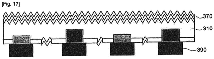
- FIGS. 11 to 17 are schematic views showing a fabrication process of a back contact solar cell according to one embodiment of the present invention. Hereinafter, the fabrication process of the back contact solar cell according to the present invention will be described with reference to FIGS. 11 to 17 .
- a texturing structure is formed on at least one of a front surface and a rear surface of a p-type silicon substrate 310.
- the texturing structure may usually be formed in a pyramid shape, etc, and performs a function of reflecting solar light incident to the solar cell so that maximum light may be absorbed into an inside of the solar cell, thereby raising efficiency of the solar cell.
- the texturing structure may be formed by etching using a known etching method.
- the texturing structure may be formed by immersing the silicon substrate 310 in a basic etching solution such as tetramethylammonium hydroxide (TMHA), potassium hydroxide (KOH), or sodium hydroxide (NaOH), etc., to which surfactant such as isopropyl alcohol (IPA), isopropyl ethanol (IPE), etc., is added.
- TMHA tetramethylammonium hydroxide
- KOH potassium hydroxide
- NaOH sodium hydroxide
- surfactant such as isopropyl alcohol (IPA), isopropyl ethanol (IPE), etc.
- thermal oxide layers 321 and 323 for surface passivation are formed on the front and rear surfaces of the silicon substrate 310.
- the passivation layers 321 and 323 have a role of stabilizing and protecting the surface and minimizing surface recombination of electron-hole pairs to increase efficiency of the solar cell.
- passivation layers 321 and 323 may be thermal oxide such as silicon oxide (SiO 2 ), etc., formed by a rapid thermal oxidation (RTO) scheme performed inside a furnace for rapid thermal processing (RTP), as described above. Also, the passivation layers 321 and 323 may be formed by a sputtering method using the silicon oxide (SiO 2 ) as a target material.
- RTO rapid thermal oxidation
- RTP rapid thermal processing
- the passivation layers 321 and 323 may be formed by a sputtering method using the silicon oxide (SiO 2 ) as a target material.
- a pattern for diffusing an n-type material is formed on the rear surface of the silicon substrate 310, as shown in FIG. 12 .
- the formation of the pattern is to partially remove the oxidation layer 323 already formed on the rear surface of the silicon substrate 310, thereby making it possible to diffuse an n-type material through the removed portion.
- a process forming the pattern by partially removing the oxide layer 323 may be performed by irradiating laser light.
- a light source of the irradiated laser light various light sources may be used; by way of example, a green laser source with a wavelength of about 532nm, an Nd/YAG laser source with a wavelength of about 1064nm, etc., may be used.
- an n-type material 330 is diffused into portions at which the oxide layer 323 is removed, as shown in FIG. 13 .
- a thermal diffusion method As a method diffusing the n-type material 330, a thermal diffusion method, etc., may be used.
- a method performing doping by inserting the p-type silicon substrate 310 into a high-temperature furnace and flowing the n-type material (for example, POCl 3 ) into an inside of the furnace may be used.
- the oxide layer 323 is removed in order to form a p-type semiconductor region in a region except for the region into which the n-type material is diffused, as shown in FIG. 14 .
- a certain amount of the oxidation layer 323 is left in a region close to the region into which the n-type material 330 is diffused in order to insulate between the region into which the n-type material 330 is diffused and the p-type semiconductor region.
- the oxide layer 323 may also be removed by irradiating green laser light with the wavelength of about 532nm, Nd/YAG laser light with the wavelength of about 1064nm, etc.
- the oxide layer 323 left in order to isolate the region into which the n-type material is diffused and the p-type semiconductor region may perform a function of a rear passivation layer of the back contact solar cell. That is, the remaining oxide layer 323 protects the rear surface of the silicon substrate 310 as well as prevents rear surface recombination of electron-hole pairs so as to be able to contribute to improvement in efficiency of the solar cell.
- the p-type semiconductor region 340 is formed by printing an aluminum (Al) metal, etc. in a region except for the region into which the n-type material is diffused, as shown in FIG. 15 .
- the printing of the aluminum (Al) metal, etc., for forming the p-type semiconductor region 340 may be performed by a screen printing method, etc., which is a well-known printing method.
- the removal of oxide layer 323 required for diffusing the n-type material 330 and the removal of the oxide layer 323 required for forming the p-type semiconductor region 340 are performed by irradiating the laser light, it is possible to omit a photolithography process requisitely used to remove the oxide layer on the rear surface of the conventional back contact solar cell. Since the photolithography process, which is a complicated and expensive process, may be omitted, it is possible to simplify the fabrication process of the back contact solar cell and also reduce fabrication costs.
- an anti-reflection coating 370 is formed on an upper surface of the oxide layer 321 formed on the front surface of the p-type silicon substrate 310, as shown in FIG. 16 .
- the anti-reflection coating 370 may be deposited using a deposition method such as a plasma enhanced chemical vapor deposition (PECVD) method, a sputtering method, or a spin coating method, etc., and be made of a material such as silicon nitride (SiN x ) or titanium dioxide (TiO 2 ), etc.
- PECVD plasma enhanced chemical vapor deposition
- SiN x silicon nitride
- TiO 2 titanium dioxide
- electrodes are printed on each of the regions into which the n-type material is diffused and the p-type semiconductor region 340 to form rear electrodes 390, thereby completing the back contact solar cell, as shown in FIG. 17 .
- a metal with a high conductivity such as silver (Ag), etc., may be used.
- the fabrication method of the back contact solar cell of the present invention it is possible to simplify a fabrication process, reduce fabrication time, and reduce fabrication costs by using the laser method instead of photolithography in forming the pattern for formation of the p-type semiconductor region and the n-type semiconductor region.
Landscapes
- Photovoltaic Devices (AREA)
- Life Sciences & Earth Sciences (AREA)
- Sustainable Development (AREA)
- Engineering & Computer Science (AREA)
- Sustainable Energy (AREA)
- Manufacturing & Machinery (AREA)
Claims (11)
- Rückkontaktsolarzelle umfassend:ein Halbleitersubstrat (310) einer leitfähigen Art mit einer texturierten Vorderfläche und einer texturierten Rückfläche und mit einer ersten leitfähigen Art;eine erste Oxidschicht (321), die auf der Vorderseite des Substrats (310) gebildet ist;mindestens einen Halbleiterbereich (330) einer ersten leitfähigen Art (330) und einen Halbleiterbereich einer zweiten leitfähigen Art (340), die in einem abwechselnden Muster in vorbestimmten Abständen auf der Rückseite des Substrats (310) ausgebildet sind, wobei der Halbleiterbereich der ersten leitfähigen Art (330) eine zweite leitfähige Art gegenüber der ersten leitfähigen Art aufweist, und der Halbleiterbereich der zweiten leitfähigen Art (340) die erste leitfähige Art und eine höhere Dotierungskonzentration als das Substrat (310) aufweist;eine zweite Oxidschicht (323), die auf der verbleibenden Rückseite des Substrats (310) mit Ausnahme des Halbleiterbereichs der ersten leitfähigen Art (330) und des Halbleiterbereichs der zweiten leitfähige Art ausgebildet ist (340); undElektroden (390), die jeweils auf dem Halbleiterbereich der ersten leitfähigen Art (330) und dem Halbleiterbereich der zweiten leitfähigen Art (340) ausgebildet sind,dadurch gekennzeichnet, dassTeile der Rückseite des Substrats (310), die dem Halbleiterbereich der ersten leitfähigen Art (330) und dem Halbleiterbereich der zweiten leitfähigen Art (340) entsprechen, nicht texturiert sind,die gesamte Vorderseite des Halbleitersubstrats der leitfähigen Art (310) texturiert ist undder texturierte Bereich auf der Vorderseite des Substrats (310) größer als ein Bereich des texturierten Bereichs auf der Rückseite des Substrats (310) ist.
- Rückkontaktsolarzelle nach Anspruch 1, wobei das Substrat (310) ein Siliziumsubstrat vom p-Typ ist.
- Rückkontaktsolarzelle nach einem der vorhergehenden Ansprüche, wobei der Halbleiterbereich der ersten leitfähigen Art (330) und der Halbleiterbereich der zweiten leitfähigen Art (340) ein Halbleiterbereich vom n-Typ (n+) bzw. vom p-Typ (P+) ist.
- Rückkontaktsolarzelle nach einem der vorhergehenden Ansprüche, wobei die erste und die zweite Oxidschicht (321, 323) Siliziumoxidschichten sind.
- Rückkontaktsolarzelle nach einem der vorhergehenden Ansprüche ferner umfassend eine Antireflexionsbeschichtung (370), die auf einer oberen Fläche der ersten Oxidschicht (321) gebildet ist.
- Rückkontaktsolarzelle nach Anspruch 5, wobei die Antireflexbeschichtung (370) eine Siliziumnitridschicht umfasst.
- Rückkontaktsolarzelle nach Anspruch 5 oder 6, wobei
die erste Oxidschicht (321) vollständig auf der Vorderseite des Substrats (310) gebildet ist und
die Antireflexbeschichtung (370) vollständig auf der ersten Oxidschicht (321) gebildet ist. - Rückkontaktsolarzelle nach einem der vorhergehenden Ansprüche, die eine Vielzahl von Halbleiterbereichen der ersten leitfähigen Art (330) umfasst, wobei
die Vielzahl von Halbleiterbereichen der ersten leitfähigen Art (330) auf der Rückseite des Halbleitersubstrats der leitfähigen Art (310) an entfernten Abschnitten der zweiten Oxidschicht (323) ausgebildet sind. - Rückkontaktsolarzelle nach einem der vorhergehenden Ansprüche, die eine Vielzahl von Halbleiterbereichen der ersten leitfähigen Art (330) und eine Vielzahl von Halbleiterbereichen der zweiten leitfähigen Art (340) umfasst, wobei die Vielzahl von Halbleiterbereichen der ersten leitfähigen Art (330) und die Vielzahl von Halbleiterbereichen der zweiten leitfähigen Art (340) in einem abwechselnden Muster ausgebildet sind.
- Rückkontaktsolarzelle nach einem der Ansprüche 1 bis 8, die eine Vielzahl von Halbleiterbereichen der ersten leitfähigen Art (330) und eine Vielzahl von Halbleiterbereichen der zweiten leitfähigen Art (340) umfasst, wobei
die Halbleiterbereiche der zweiten leitfähigen Art (340) an entfernten Abschnitten der zweiten Oxidschicht (323) zwischen den Halbleiterbereichen der ersten leitfähigen Art (330) in vorbestimmten Abständen von den Halbleiterbereichen der ersten leitfähigen Art (330) gebildet sind. - Rückkontaktsolarzelle nach einem der vorhergehenden Ansprüche, wobei die Elektroden (390) umfassen
eine erste Elektrode, die elektrisch mit dem Halbleiterbereich der ersten leitfähigen Art (330) verbunden ist; und
eine zweite Elektrode, die elektrisch mit dem Halbleiterbereich der zweiten leitfähigen Art (340) verbunden ist.
Applications Claiming Priority (3)
| Application Number | Priority Date | Filing Date | Title |
|---|---|---|---|
| KR1020080016725A KR101155343B1 (ko) | 2008-02-25 | 2008-02-25 | 백 콘택 태양전지의 제조 방법 |
| EP08872993.4A EP2257991B1 (de) | 2008-02-25 | 2008-11-13 | Herstellungsverfahren für rückkontakt-solarzelle |
| PCT/KR2008/006685 WO2009107920A1 (en) | 2008-02-25 | 2008-11-13 | Back contact solar cell and fabrication method thereof |
Related Parent Applications (2)
| Application Number | Title | Priority Date | Filing Date |
|---|---|---|---|
| EP08872993.4A Division EP2257991B1 (de) | 2008-02-25 | 2008-11-13 | Herstellungsverfahren für rückkontakt-solarzelle |
| EP08872993.4A Division-Into EP2257991B1 (de) | 2008-02-25 | 2008-11-13 | Herstellungsverfahren für rückkontakt-solarzelle |
Publications (2)
| Publication Number | Publication Date |
|---|---|
| EP2993707A1 EP2993707A1 (de) | 2016-03-09 |
| EP2993707B1 true EP2993707B1 (de) | 2020-04-22 |
Family
ID=41016274
Family Applications (2)
| Application Number | Title | Priority Date | Filing Date |
|---|---|---|---|
| EP15191649.1A Active EP2993707B1 (de) | 2008-02-25 | 2008-11-13 | Rückkontakt-solarzelle mit texturierter front- und rückseitenoberfläche |
| EP08872993.4A Active EP2257991B1 (de) | 2008-02-25 | 2008-11-13 | Herstellungsverfahren für rückkontakt-solarzelle |
Family Applications After (1)
| Application Number | Title | Priority Date | Filing Date |
|---|---|---|---|
| EP08872993.4A Active EP2257991B1 (de) | 2008-02-25 | 2008-11-13 | Herstellungsverfahren für rückkontakt-solarzelle |
Country Status (4)
| Country | Link |
|---|---|
| US (6) | US11843063B2 (de) |
| EP (2) | EP2993707B1 (de) |
| KR (1) | KR101155343B1 (de) |
| WO (1) | WO2009107920A1 (de) |
Families Citing this family (34)
| Publication number | Priority date | Publication date | Assignee | Title |
|---|---|---|---|---|
| WO2011072161A2 (en) * | 2009-12-09 | 2011-06-16 | Solexel, Inc. | High-efficiency photovoltaic back-contact solar cell structures and manufacturing methods using thin planar semiconductors |
| US8053867B2 (en) | 2008-08-20 | 2011-11-08 | Honeywell International Inc. | Phosphorous-comprising dopants and methods for forming phosphorous-doped regions in semiconductor substrates using phosphorous-comprising dopants |
| US7951696B2 (en) | 2008-09-30 | 2011-05-31 | Honeywell International Inc. | Methods for simultaneously forming N-type and P-type doped regions using non-contact printing processes |
| US8518170B2 (en) | 2008-12-29 | 2013-08-27 | Honeywell International Inc. | Boron-comprising inks for forming boron-doped regions in semiconductor substrates using non-contact printing processes and methods for fabricating such boron-comprising inks |
| US8324089B2 (en) | 2009-07-23 | 2012-12-04 | Honeywell International Inc. | Compositions for forming doped regions in semiconductor substrates, methods for fabricating such compositions, and methods for forming doped regions using such compositions |
| US8324015B2 (en) * | 2009-12-01 | 2012-12-04 | Sunpower Corporation | Solar cell contact formation using laser ablation |
| CN102222717A (zh) * | 2010-04-16 | 2011-10-19 | 益通光能科技股份有限公司 | 形成太阳能电池的方法 |
| TWI514599B (zh) | 2010-06-18 | 2015-12-21 | Semiconductor Energy Lab | 光電轉換裝置及其製造方法 |
| MY158500A (en) | 2010-08-05 | 2016-10-14 | Solexel Inc | Backplane reinforcement and interconnects for solar cells |
| KR101657626B1 (ko) * | 2010-10-08 | 2016-09-19 | 주식회사 원익아이피에스 | 태양전지제조방법 및 그 방법에 의하여 제조된 태양전지 |
| KR101219241B1 (ko) * | 2011-05-18 | 2013-01-21 | 현대중공업 주식회사 | 후면전극형 태양전지 및 그 제조방법 |
| KR101286290B1 (ko) * | 2011-05-31 | 2013-07-15 | 현대중공업 주식회사 | 후면접합형 태양전지 및 그 제조방법 |
| JP2014525671A (ja) * | 2011-08-09 | 2014-09-29 | ソレクセル、インコーポレイテッド | 薄い結晶半導体吸収体を使用する高効率ソーラー光発電セルおよびモジュール |
| US8629294B2 (en) | 2011-08-25 | 2014-01-14 | Honeywell International Inc. | Borate esters, boron-comprising dopants, and methods of fabricating boron-comprising dopants |
| US8975170B2 (en) | 2011-10-24 | 2015-03-10 | Honeywell International Inc. | Dopant ink compositions for forming doped regions in semiconductor substrates, and methods for fabricating dopant ink compositions |
| US20130146136A1 (en) * | 2011-12-13 | 2013-06-13 | Kyoung-Jin Seo | Photovoltaic device and method of manufacturing the same |
| DE112012005381T5 (de) * | 2011-12-21 | 2014-09-04 | Sunpower Corp. | Hybride Polysilizium-Heteroübergangs-Rückseitenkontaktzelle |
| US8597970B2 (en) | 2011-12-21 | 2013-12-03 | Sunpower Corporation | Hybrid polysilicon heterojunction back contact cell |
| US8679889B2 (en) | 2011-12-21 | 2014-03-25 | Sunpower Corporation | Hybrid polysilicon heterojunction back contact cell |
| KR101894584B1 (ko) * | 2012-01-09 | 2018-09-04 | 엘지전자 주식회사 | 이온 주입 장치 |
| KR101649060B1 (ko) * | 2012-03-12 | 2016-08-17 | 미쓰비시덴키 가부시키가이샤 | 태양전지 셀의 제조 방법 |
| FI20125988A7 (fi) * | 2012-09-24 | 2014-03-25 | Optitune Oy | Menetelmä n-tyypin piisubstraatin modifioimiseksi |
| CN102931255B (zh) * | 2012-11-20 | 2016-04-27 | 上饶光电高科技有限公司 | 一种背接触太阳能电池及其制造方法 |
| DE102013219603A1 (de) * | 2013-09-27 | 2015-04-02 | International Solar Energy Research Center Konstanz E.V. | Verfahren zur Herstellung einer Solarzelle |
| CN106687617B (zh) * | 2014-07-15 | 2020-04-07 | 奈特考尔技术公司 | 激光转印ibc太阳能电池 |
| US9583649B2 (en) * | 2015-06-22 | 2017-02-28 | International Business Machines Corporation | Thin film solar cell backside contact manufacturing process |
| CN107611183B (zh) * | 2016-06-30 | 2020-06-19 | 比亚迪股份有限公司 | 电池片、电池片矩阵、太阳能电池及电池片的制备方法 |
| JP6330108B1 (ja) * | 2016-11-07 | 2018-05-23 | 信越化学工業株式会社 | 高光電変換効率太陽電池及び高光電変換効率太陽電池の製造方法 |
| CN114256381B (zh) * | 2021-11-08 | 2024-01-16 | 西安隆基乐叶光伏科技有限公司 | N型TopCon电池片及其制备方法 |
| CN116741850A (zh) * | 2022-06-08 | 2023-09-12 | 浙江晶科能源有限公司 | 一种太阳能电池及光伏组件 |
| CN117476785A (zh) * | 2022-06-21 | 2024-01-30 | 浙江晶科能源有限公司 | 背接触太阳能电池及光伏组件 |
| KR20240158332A (ko) * | 2022-09-08 | 2024-11-04 | 쟝쑤 리드마이크로 나노 테크놀러지 컴퍼니 리미티드 | 전하 저장 구조물 및 이를 제조하기 위한 방법 |
| CN117637875A (zh) * | 2024-01-26 | 2024-03-01 | 隆基绿能科技股份有限公司 | 一种背接触电池及其制造方法 |
| CN119317233B (zh) * | 2024-12-13 | 2025-03-28 | 常州正宇光伏科技有限公司 | 一种隧穿氧化钝化接触的背接触太阳能电池制备方法 |
Family Cites Families (15)
| Publication number | Priority date | Publication date | Assignee | Title |
|---|---|---|---|---|
| US4665277A (en) | 1986-03-11 | 1987-05-12 | The United States Of America As Represented By The Administrator Of The National Aeronautics And Space Administration | Floating emitter solar cell |
| US4927770A (en) * | 1988-11-14 | 1990-05-22 | Electric Power Research Inst. Corp. Of District Of Columbia | Method of fabricating back surface point contact solar cells |
| US5053083A (en) * | 1989-05-08 | 1991-10-01 | The Board Of Trustees Of The Leland Stanford Junior University | Bilevel contact solar cells |
| US5356488A (en) * | 1991-12-27 | 1994-10-18 | Rudolf Hezel | Solar cell and method for its manufacture |
| US7388147B2 (en) * | 2003-04-10 | 2008-06-17 | Sunpower Corporation | Metal contact structure for solar cell and method of manufacture |
| US7649141B2 (en) * | 2003-06-30 | 2010-01-19 | Advent Solar, Inc. | Emitter wrap-through back contact solar cells on thin silicon wafers |
| US20060060238A1 (en) * | 2004-02-05 | 2006-03-23 | Advent Solar, Inc. | Process and fabrication methods for emitter wrap through back contact solar cells |
| US20050172996A1 (en) * | 2004-02-05 | 2005-08-11 | Advent Solar, Inc. | Contact fabrication of emitter wrap-through back contact silicon solar cells |
| US20070169806A1 (en) * | 2006-01-20 | 2007-07-26 | Palo Alto Research Center Incorporated | Solar cell production using non-contact patterning and direct-write metallization |
| EP1863100A1 (de) | 2006-05-30 | 2007-12-05 | INTERUNIVERSITAIR MICROELEKTRONICA CENTRUM vzw (IMEC) | Verfahren zur Herstellung von dünnen Substraten |
| US7805064B2 (en) | 2006-06-26 | 2010-09-28 | TP Solar, Inc. (Corporation of CA, USA) | Rapid thermal firing IR conveyor furnace having high intensity heating section |
| US20080000522A1 (en) | 2006-06-30 | 2008-01-03 | General Electric Company | Photovoltaic device which includes all-back-contact configuration; and related processes |
| US20080173347A1 (en) * | 2007-01-23 | 2008-07-24 | General Electric Company | Method And Apparatus For A Semiconductor Structure |
| CN103077978B (zh) * | 2007-02-16 | 2016-12-28 | 纳克公司 | 太阳能电池结构、光生伏打模块及对应的工艺 |
| US20090242031A1 (en) | 2008-03-27 | 2009-10-01 | Twin Creeks Technologies, Inc. | Photovoltaic Assembly Including a Conductive Layer Between a Semiconductor Lamina and a Receiver Element |
-
2008
- 2008-02-25 KR KR1020080016725A patent/KR101155343B1/ko not_active Expired - Fee Related
- 2008-11-13 WO PCT/KR2008/006685 patent/WO2009107920A1/en not_active Ceased
- 2008-11-13 EP EP15191649.1A patent/EP2993707B1/de active Active
- 2008-11-13 US US12/812,910 patent/US11843063B2/en active Active
- 2008-11-13 EP EP08872993.4A patent/EP2257991B1/de active Active
-
2015
- 2015-09-01 US US14/842,635 patent/US20150380575A1/en not_active Abandoned
- 2015-12-29 US US14/983,282 patent/US20160111565A1/en not_active Abandoned
-
2023
- 2023-11-07 US US18/504,051 patent/US12136677B2/en active Active
-
2024
- 2024-10-03 US US18/906,003 patent/US12532571B2/en active Active
-
2025
- 2025-11-21 US US19/397,194 patent/US20260082726A1/en active Pending
Non-Patent Citations (1)
| Title |
|---|
| KNOBLOCH J ET AL: "High-efficiency solar cells from FZ, CZ and MC silicon material", PROCEEDINGS OF THE PHOTOVOLTAIC SPECIALISTS CONFERENCE. LOUISVILLE, MAY 10 - 14, 19; [PROCEEDINGS OF THE PHOTOVOLTAIC SPECIALISTS CONFERENCE], NEW YORK, IEEE, US, vol. CONF. 23, 10 May 1993 (1993-05-10), pages 271 - 276, XP010113395, ISBN: 978-0-7803-1220-3, DOI: 10.1109/PVSC.1993.347172 * |
Also Published As
| Publication number | Publication date |
|---|---|
| US20240097061A1 (en) | 2024-03-21 |
| EP2257991A1 (de) | 2010-12-08 |
| EP2257991A4 (de) | 2013-04-10 |
| US20150380575A1 (en) | 2015-12-31 |
| EP2993707A1 (de) | 2016-03-09 |
| US12136677B2 (en) | 2024-11-05 |
| EP2257991B1 (de) | 2016-01-27 |
| US20160111565A1 (en) | 2016-04-21 |
| WO2009107920A1 (en) | 2009-09-03 |
| US11843063B2 (en) | 2023-12-12 |
| US12532571B2 (en) | 2026-01-20 |
| KR101155343B1 (ko) | 2012-06-11 |
| US20110100457A1 (en) | 2011-05-05 |
| US20250031481A1 (en) | 2025-01-23 |
| KR20090091456A (ko) | 2009-08-28 |
| US20260082726A1 (en) | 2026-03-19 |
Similar Documents
| Publication | Publication Date | Title |
|---|---|---|
| US12532571B2 (en) | Back contact solar cell and fabrication method thereof | |
| US9087956B2 (en) | Solar cell and fabrication method thereof | |
| US9583653B2 (en) | Solar cell and fabrication method thereof | |
| US8969125B2 (en) | Solar cell and method for manufacturing the same | |
| KR20090091562A (ko) | 태양전지 및 그 제조방법 | |
| US20110017258A1 (en) | Solar cell and fabrication method thereof | |
| KR20110097827A (ko) | 깊은 홈 후측 콘택 광발전 태양 전지들 | |
| WO2010064303A1 (ja) | 太陽電池セルの製造方法 | |
| KR101085382B1 (ko) | 선택적 에미터를 포함하는 태양 전지 제조 방법 | |
| KR101360658B1 (ko) | 태양전지의 선택적 에미터 형성방법 | |
| US8993423B2 (en) | Method for manufacturing solar cell | |
| KR101125450B1 (ko) | 후면전극형 태양전지의 제조방법 | |
| KR101155192B1 (ko) | 태양전지의 제조방법 | |
| KR20110078549A (ko) | 태양전지의 선택적 에미터 형성방법 | |
| JP2007019259A (ja) | 太陽電池およびその製造方法 | |
| CN120239367B (zh) | 太阳能电池片及其制备方法和光伏组件 | |
| KR101137068B1 (ko) | 후면전극형 태양전지의 제조방법 | |
| KR20120026736A (ko) | 태양전지 제조 시의 선택적 에미터 형성 방법 | |
| KR20120077709A (ko) | 국부화 에미터 태양전지 및 그 제조 방법 | |
| HK1169212B (en) | Manufacturing method of bifacial solar cells | |
| HK1169212A (en) | Manufacturing method of bifacial solar cells | |
| KR20120094215A (ko) | 태양전지의 선택적 에미터 형성방법 |
Legal Events
| Date | Code | Title | Description |
|---|---|---|---|
| PUAI | Public reference made under article 153(3) epc to a published international application that has entered the european phase |
Free format text: ORIGINAL CODE: 0009012 |
|
| 17P | Request for examination filed |
Effective date: 20151027 |
|
| AC | Divisional application: reference to earlier application |
Ref document number: 2257991 Country of ref document: EP Kind code of ref document: P |
|
| AK | Designated contracting states |
Kind code of ref document: A1 Designated state(s): AT BE BG CH CY CZ DE DK EE ES FI FR GB GR HR HU IE IS IT LI LT LU LV MC MT NL NO PL PT RO SE SI SK TR |
|
| STAA | Information on the status of an ep patent application or granted ep patent |
Free format text: STATUS: EXAMINATION IS IN PROGRESS |
|
| 17Q | First examination report despatched |
Effective date: 20190626 |
|
| GRAP | Despatch of communication of intention to grant a patent |
Free format text: ORIGINAL CODE: EPIDOSNIGR1 |
|
| STAA | Information on the status of an ep patent application or granted ep patent |
Free format text: STATUS: GRANT OF PATENT IS INTENDED |
|
| INTG | Intention to grant announced |
Effective date: 20191128 |
|
| RIN1 | Information on inventor provided before grant (corrected) |
Inventor name: JUNG, IL-HYOUNG Inventor name: KIM, BUM-SUNG Inventor name: KIM, JONG-HWAN Inventor name: YUN, JU-HWAN Inventor name: KIM, HWA-NYEON Inventor name: KIM, JIN-AH |
|
| GRAS | Grant fee paid |
Free format text: ORIGINAL CODE: EPIDOSNIGR3 |
|
| GRAA | (expected) grant |
Free format text: ORIGINAL CODE: 0009210 |
|
| STAA | Information on the status of an ep patent application or granted ep patent |
Free format text: STATUS: THE PATENT HAS BEEN GRANTED |
|
| AC | Divisional application: reference to earlier application |
Ref document number: 2257991 Country of ref document: EP Kind code of ref document: P |
|
| AK | Designated contracting states |
Kind code of ref document: B1 Designated state(s): AT BE BG CH CY CZ DE DK EE ES FI FR GB GR HR HU IE IS IT LI LT LU LV MC MT NL NO PL PT RO SE SI SK TR |
|
| REG | Reference to a national code |
Ref country code: CH Ref legal event code: EP |
|
| REG | Reference to a national code |
Ref country code: DE Ref legal event code: R096 Ref document number: 602008062572 Country of ref document: DE |
|
| REG | Reference to a national code |
Ref country code: IE Ref legal event code: FG4D |
|
| REG | Reference to a national code |
Ref country code: AT Ref legal event code: REF Ref document number: 1261290 Country of ref document: AT Kind code of ref document: T Effective date: 20200515 |
|
| REG | Reference to a national code |
Ref country code: LT Ref legal event code: MG4D |
|
| REG | Reference to a national code |
Ref country code: NL Ref legal event code: MP Effective date: 20200422 |
|
| PG25 | Lapsed in a contracting state [announced via postgrant information from national office to epo] |
Ref country code: IS Free format text: LAPSE BECAUSE OF FAILURE TO SUBMIT A TRANSLATION OF THE DESCRIPTION OR TO PAY THE FEE WITHIN THE PRESCRIBED TIME-LIMIT Effective date: 20200822 Ref country code: GR Free format text: LAPSE BECAUSE OF FAILURE TO SUBMIT A TRANSLATION OF THE DESCRIPTION OR TO PAY THE FEE WITHIN THE PRESCRIBED TIME-LIMIT Effective date: 20200723 Ref country code: NO Free format text: LAPSE BECAUSE OF FAILURE TO SUBMIT A TRANSLATION OF THE DESCRIPTION OR TO PAY THE FEE WITHIN THE PRESCRIBED TIME-LIMIT Effective date: 20200722 Ref country code: FI Free format text: LAPSE BECAUSE OF FAILURE TO SUBMIT A TRANSLATION OF THE DESCRIPTION OR TO PAY THE FEE WITHIN THE PRESCRIBED TIME-LIMIT Effective date: 20200422 Ref country code: NL Free format text: LAPSE BECAUSE OF FAILURE TO SUBMIT A TRANSLATION OF THE DESCRIPTION OR TO PAY THE FEE WITHIN THE PRESCRIBED TIME-LIMIT Effective date: 20200422 Ref country code: SE Free format text: LAPSE BECAUSE OF FAILURE TO SUBMIT A TRANSLATION OF THE DESCRIPTION OR TO PAY THE FEE WITHIN THE PRESCRIBED TIME-LIMIT Effective date: 20200422 Ref country code: PT Free format text: LAPSE BECAUSE OF FAILURE TO SUBMIT A TRANSLATION OF THE DESCRIPTION OR TO PAY THE FEE WITHIN THE PRESCRIBED TIME-LIMIT Effective date: 20200824 Ref country code: LT Free format text: LAPSE BECAUSE OF FAILURE TO SUBMIT A TRANSLATION OF THE DESCRIPTION OR TO PAY THE FEE WITHIN THE PRESCRIBED TIME-LIMIT Effective date: 20200422 |
|
| REG | Reference to a national code |
Ref country code: AT Ref legal event code: MK05 Ref document number: 1261290 Country of ref document: AT Kind code of ref document: T Effective date: 20200422 |
|
| PG25 | Lapsed in a contracting state [announced via postgrant information from national office to epo] |
Ref country code: BG Free format text: LAPSE BECAUSE OF FAILURE TO SUBMIT A TRANSLATION OF THE DESCRIPTION OR TO PAY THE FEE WITHIN THE PRESCRIBED TIME-LIMIT Effective date: 20200722 Ref country code: LV Free format text: LAPSE BECAUSE OF FAILURE TO SUBMIT A TRANSLATION OF THE DESCRIPTION OR TO PAY THE FEE WITHIN THE PRESCRIBED TIME-LIMIT Effective date: 20200422 Ref country code: HR Free format text: LAPSE BECAUSE OF FAILURE TO SUBMIT A TRANSLATION OF THE DESCRIPTION OR TO PAY THE FEE WITHIN THE PRESCRIBED TIME-LIMIT Effective date: 20200422 |
|
| REG | Reference to a national code |
Ref country code: DE Ref legal event code: R097 Ref document number: 602008062572 Country of ref document: DE |
|
| PG25 | Lapsed in a contracting state [announced via postgrant information from national office to epo] |
Ref country code: AT Free format text: LAPSE BECAUSE OF FAILURE TO SUBMIT A TRANSLATION OF THE DESCRIPTION OR TO PAY THE FEE WITHIN THE PRESCRIBED TIME-LIMIT Effective date: 20200422 Ref country code: EE Free format text: LAPSE BECAUSE OF FAILURE TO SUBMIT A TRANSLATION OF THE DESCRIPTION OR TO PAY THE FEE WITHIN THE PRESCRIBED TIME-LIMIT Effective date: 20200422 Ref country code: DK Free format text: LAPSE BECAUSE OF FAILURE TO SUBMIT A TRANSLATION OF THE DESCRIPTION OR TO PAY THE FEE WITHIN THE PRESCRIBED TIME-LIMIT Effective date: 20200422 Ref country code: RO Free format text: LAPSE BECAUSE OF FAILURE TO SUBMIT A TRANSLATION OF THE DESCRIPTION OR TO PAY THE FEE WITHIN THE PRESCRIBED TIME-LIMIT Effective date: 20200422 Ref country code: IT Free format text: LAPSE BECAUSE OF FAILURE TO SUBMIT A TRANSLATION OF THE DESCRIPTION OR TO PAY THE FEE WITHIN THE PRESCRIBED TIME-LIMIT Effective date: 20200422 Ref country code: CZ Free format text: LAPSE BECAUSE OF FAILURE TO SUBMIT A TRANSLATION OF THE DESCRIPTION OR TO PAY THE FEE WITHIN THE PRESCRIBED TIME-LIMIT Effective date: 20200422 Ref country code: ES Free format text: LAPSE BECAUSE OF FAILURE TO SUBMIT A TRANSLATION OF THE DESCRIPTION OR TO PAY THE FEE WITHIN THE PRESCRIBED TIME-LIMIT Effective date: 20200422 |
|
| PG25 | Lapsed in a contracting state [announced via postgrant information from national office to epo] |
Ref country code: PL Free format text: LAPSE BECAUSE OF FAILURE TO SUBMIT A TRANSLATION OF THE DESCRIPTION OR TO PAY THE FEE WITHIN THE PRESCRIBED TIME-LIMIT Effective date: 20200422 Ref country code: SK Free format text: LAPSE BECAUSE OF FAILURE TO SUBMIT A TRANSLATION OF THE DESCRIPTION OR TO PAY THE FEE WITHIN THE PRESCRIBED TIME-LIMIT Effective date: 20200422 |
|
| PLBE | No opposition filed within time limit |
Free format text: ORIGINAL CODE: 0009261 |
|
| STAA | Information on the status of an ep patent application or granted ep patent |
Free format text: STATUS: NO OPPOSITION FILED WITHIN TIME LIMIT |
|
| 26N | No opposition filed |
Effective date: 20210125 |
|
| PG25 | Lapsed in a contracting state [announced via postgrant information from national office to epo] |
Ref country code: SI Free format text: LAPSE BECAUSE OF FAILURE TO SUBMIT A TRANSLATION OF THE DESCRIPTION OR TO PAY THE FEE WITHIN THE PRESCRIBED TIME-LIMIT Effective date: 20200422 |
|
| PG25 | Lapsed in a contracting state [announced via postgrant information from national office to epo] |
Ref country code: MC Free format text: LAPSE BECAUSE OF FAILURE TO SUBMIT A TRANSLATION OF THE DESCRIPTION OR TO PAY THE FEE WITHIN THE PRESCRIBED TIME-LIMIT Effective date: 20200422 |
|
| REG | Reference to a national code |
Ref country code: CH Ref legal event code: PL |
|
| GBPC | Gb: european patent ceased through non-payment of renewal fee |
Effective date: 20201113 |
|
| PG25 | Lapsed in a contracting state [announced via postgrant information from national office to epo] |
Ref country code: LU Free format text: LAPSE BECAUSE OF NON-PAYMENT OF DUE FEES Effective date: 20201113 |
|
| REG | Reference to a national code |
Ref country code: BE Ref legal event code: MM Effective date: 20201130 |
|
| PG25 | Lapsed in a contracting state [announced via postgrant information from national office to epo] |
Ref country code: CH Free format text: LAPSE BECAUSE OF NON-PAYMENT OF DUE FEES Effective date: 20201130 Ref country code: LI Free format text: LAPSE BECAUSE OF NON-PAYMENT OF DUE FEES Effective date: 20201130 |
|
| PG25 | Lapsed in a contracting state [announced via postgrant information from national office to epo] |
Ref country code: IE Free format text: LAPSE BECAUSE OF NON-PAYMENT OF DUE FEES Effective date: 20201113 Ref country code: FR Free format text: LAPSE BECAUSE OF NON-PAYMENT OF DUE FEES Effective date: 20201130 |
|
| PG25 | Lapsed in a contracting state [announced via postgrant information from national office to epo] |
Ref country code: GB Free format text: LAPSE BECAUSE OF NON-PAYMENT OF DUE FEES Effective date: 20201113 |
|
| PG25 | Lapsed in a contracting state [announced via postgrant information from national office to epo] |
Ref country code: TR Free format text: LAPSE BECAUSE OF FAILURE TO SUBMIT A TRANSLATION OF THE DESCRIPTION OR TO PAY THE FEE WITHIN THE PRESCRIBED TIME-LIMIT Effective date: 20200422 Ref country code: MT Free format text: LAPSE BECAUSE OF FAILURE TO SUBMIT A TRANSLATION OF THE DESCRIPTION OR TO PAY THE FEE WITHIN THE PRESCRIBED TIME-LIMIT Effective date: 20200422 Ref country code: CY Free format text: LAPSE BECAUSE OF FAILURE TO SUBMIT A TRANSLATION OF THE DESCRIPTION OR TO PAY THE FEE WITHIN THE PRESCRIBED TIME-LIMIT Effective date: 20200422 |
|
| PG25 | Lapsed in a contracting state [announced via postgrant information from national office to epo] |
Ref country code: BE Free format text: LAPSE BECAUSE OF NON-PAYMENT OF DUE FEES Effective date: 20201130 |
|
| REG | Reference to a national code |
Ref country code: DE Ref legal event code: R081 Ref document number: 602008062572 Country of ref document: DE Owner name: SHANGRAO JINKO SOLAR TECHNOLOGY DEVELOPMENT CO, CN Free format text: FORMER OWNER: LG ELECTRONICS INC., SEOUL, KR Ref country code: DE Ref legal event code: R082 Ref document number: 602008062572 Country of ref document: DE Representative=s name: DREISS PATENTANWAELTE PARTG MBB, DE Ref country code: DE Ref legal event code: R081 Ref document number: 602008062572 Country of ref document: DE Owner name: SHANGRAO XINYUAN YUEDONG TECHNOLOGY DEVELOPMEN, CN Free format text: FORMER OWNER: LG ELECTRONICS INC., SEOUL, KR |
|
| REG | Reference to a national code |
Ref country code: DE Ref legal event code: R081 Ref document number: 602008062572 Country of ref document: DE Owner name: SHANGRAO XINYUAN YUEDONG TECHNOLOGY DEVELOPMEN, CN Free format text: FORMER OWNER: SHANGRAO JINKO SOLAR TECHNOLOGY DEVELOPMENT CO., LTD, SHANGRAO, JIANGXI PROVINCE, CN |
|
| REG | Reference to a national code |
Ref country code: DE Ref legal event code: R079 Ref document number: 602008062572 Country of ref document: DE Free format text: PREVIOUS MAIN CLASS: H01L0031068000 Ipc: H10F0010140000 |
|
| PG25 | Lapsed in a contracting state [announced via postgrant information from national office to epo] |
Ref country code: IS Free format text: LAPSE BECAUSE OF NON-PAYMENT OF DUE FEES Effective date: 20200822 |
|
| PGFP | Annual fee paid to national office [announced via postgrant information from national office to epo] |
Ref country code: DE Payment date: 20251119 Year of fee payment: 18 |