EP2993682A1 - Procédé permettant de réaliser une spectroscopie dans un microscope à particules chargées de transmission - Google Patents
Procédé permettant de réaliser une spectroscopie dans un microscope à particules chargées de transmission Download PDFInfo
- Publication number
- EP2993682A1 EP2993682A1 EP14183576.9A EP14183576A EP2993682A1 EP 2993682 A1 EP2993682 A1 EP 2993682A1 EP 14183576 A EP14183576 A EP 14183576A EP 2993682 A1 EP2993682 A1 EP 2993682A1
- Authority
- EP
- European Patent Office
- Prior art keywords
- specimen
- sensor
- detector
- array
- flux
- Prior art date
- Legal status (The legal status is an assumption and is not a legal conclusion. Google has not performed a legal analysis and makes no representation as to the accuracy of the status listed.)
- Withdrawn
Links
Images

Classifications
-
- H—ELECTRICITY
- H01—ELECTRIC ELEMENTS
- H01J—ELECTRIC DISCHARGE TUBES OR DISCHARGE LAMPS
- H01J37/00—Discharge tubes with provision for introducing objects or material to be exposed to the discharge, e.g. for the purpose of examination or processing thereof
- H01J37/02—Details
- H01J37/22—Optical or photographic arrangements associated with the tube
- H01J37/226—Optical arrangements for illuminating the object; optical arrangements for collecting light from the object
-
- H—ELECTRICITY
- H01—ELECTRIC ELEMENTS
- H01J—ELECTRIC DISCHARGE TUBES OR DISCHARGE LAMPS
- H01J37/00—Discharge tubes with provision for introducing objects or material to be exposed to the discharge, e.g. for the purpose of examination or processing thereof
- H01J37/02—Details
- H01J37/04—Arrangements of electrodes and associated parts for generating or controlling the discharge, e.g. electron-optical arrangement, ion-optical arrangement
- H01J37/05—Electron or ion-optical arrangements for separating electrons or ions according to their energy or mass
-
- H—ELECTRICITY
- H01—ELECTRIC ELEMENTS
- H01J—ELECTRIC DISCHARGE TUBES OR DISCHARGE LAMPS
- H01J37/00—Discharge tubes with provision for introducing objects or material to be exposed to the discharge, e.g. for the purpose of examination or processing thereof
- H01J37/02—Details
- H01J37/04—Arrangements of electrodes and associated parts for generating or controlling the discharge, e.g. electron-optical arrangement, ion-optical arrangement
- H01J37/09—Diaphragms; Shields associated with electron or ion-optical arrangements; Compensation of disturbing fields
-
- H—ELECTRICITY
- H01—ELECTRIC ELEMENTS
- H01J—ELECTRIC DISCHARGE TUBES OR DISCHARGE LAMPS
- H01J37/00—Discharge tubes with provision for introducing objects or material to be exposed to the discharge, e.g. for the purpose of examination or processing thereof
- H01J37/02—Details
- H01J37/04—Arrangements of electrodes and associated parts for generating or controlling the discharge, e.g. electron-optical arrangement, ion-optical arrangement
- H01J37/147—Arrangements for directing or deflecting the discharge along a desired path
-
- H—ELECTRICITY
- H01—ELECTRIC ELEMENTS
- H01J—ELECTRIC DISCHARGE TUBES OR DISCHARGE LAMPS
- H01J37/00—Discharge tubes with provision for introducing objects or material to be exposed to the discharge, e.g. for the purpose of examination or processing thereof
- H01J37/02—Details
- H01J37/20—Means for supporting or positioning the objects or the material; Means for adjusting diaphragms or lenses associated with the support
-
- H—ELECTRICITY
- H01—ELECTRIC ELEMENTS
- H01J—ELECTRIC DISCHARGE TUBES OR DISCHARGE LAMPS
- H01J37/00—Discharge tubes with provision for introducing objects or material to be exposed to the discharge, e.g. for the purpose of examination or processing thereof
- H01J37/02—Details
- H01J37/244—Detectors; Associated components or circuits therefor
-
- H—ELECTRICITY
- H01—ELECTRIC ELEMENTS
- H01J—ELECTRIC DISCHARGE TUBES OR DISCHARGE LAMPS
- H01J37/00—Discharge tubes with provision for introducing objects or material to be exposed to the discharge, e.g. for the purpose of examination or processing thereof
- H01J37/26—Electron or ion microscopes; Electron or ion diffraction tubes
- H01J37/261—Details
-
- H—ELECTRICITY
- H01—ELECTRIC ELEMENTS
- H01J—ELECTRIC DISCHARGE TUBES OR DISCHARGE LAMPS
- H01J37/00—Discharge tubes with provision for introducing objects or material to be exposed to the discharge, e.g. for the purpose of examination or processing thereof
- H01J37/26—Electron or ion microscopes; Electron or ion diffraction tubes
- H01J37/28—Electron or ion microscopes; Electron or ion diffraction tubes with scanning beams
-
- H—ELECTRICITY
- H01—ELECTRIC ELEMENTS
- H01J—ELECTRIC DISCHARGE TUBES OR DISCHARGE LAMPS
- H01J2237/00—Discharge tubes exposing object to beam, e.g. for analysis treatment, etching, imaging
- H01J2237/04—Means for controlling the discharge
- H01J2237/045—Diaphragms
- H01J2237/0455—Diaphragms with variable aperture
-
- H—ELECTRICITY
- H01—ELECTRIC ELEMENTS
- H01J—ELECTRIC DISCHARGE TUBES OR DISCHARGE LAMPS
- H01J2237/00—Discharge tubes exposing object to beam, e.g. for analysis treatment, etching, imaging
- H01J2237/05—Arrangements for energy or mass analysis
- H01J2237/057—Energy or mass filtering
-
- H—ELECTRICITY
- H01—ELECTRIC ELEMENTS
- H01J—ELECTRIC DISCHARGE TUBES OR DISCHARGE LAMPS
- H01J2237/00—Discharge tubes exposing object to beam, e.g. for analysis treatment, etching, imaging
- H01J2237/15—Means for deflecting or directing discharge
-
- H—ELECTRICITY
- H01—ELECTRIC ELEMENTS
- H01J—ELECTRIC DISCHARGE TUBES OR DISCHARGE LAMPS
- H01J2237/00—Discharge tubes exposing object to beam, e.g. for analysis treatment, etching, imaging
- H01J2237/20—Positioning, supporting, modifying or maintaining the physical state of objects being observed or treated
- H01J2237/2007—Holding mechanisms
-
- H—ELECTRICITY
- H01—ELECTRIC ELEMENTS
- H01J—ELECTRIC DISCHARGE TUBES OR DISCHARGE LAMPS
- H01J2237/00—Discharge tubes exposing object to beam, e.g. for analysis treatment, etching, imaging
- H01J2237/244—Detection characterized by the detecting means
- H01J2237/24485—Energy spectrometers
-
- H—ELECTRICITY
- H01—ELECTRIC ELEMENTS
- H01J—ELECTRIC DISCHARGE TUBES OR DISCHARGE LAMPS
- H01J2237/00—Discharge tubes exposing object to beam, e.g. for analysis treatment, etching, imaging
- H01J2237/245—Detection characterised by the variable being measured
- H01J2237/24571—Measurements of non-electric or non-magnetic variables
- H01J2237/24585—Other variables, e.g. energy, mass, velocity, time, temperature
-
- H—ELECTRICITY
- H01—ELECTRIC ELEMENTS
- H01J—ELECTRIC DISCHARGE TUBES OR DISCHARGE LAMPS
- H01J2237/00—Discharge tubes exposing object to beam, e.g. for analysis treatment, etching, imaging
- H01J2237/26—Electron or ion microscopes
- H01J2237/28—Scanning microscopes
- H01J2237/2802—Transmission microscopes
Definitions
- the invention relates to a method of performing spectroscopy in a Transmission Charged-Particle Microscope comprising:
- the invention also relates to a Transmission Charged-Particle Microscope in which such a method can be performed.
- Charged-particle microscopy is a well-known and increasingly important technique for imaging microscopic objects, particularly in the form of electron microscopy.
- the basic genus of electron microscope has undergone evolution into a number of well-known apparatus species, such as the Transmission Electron Microscope (TEM), Scanning Electron Microscope (SEM), and Scanning Transmission Electron Microscope (STEM), and also into various sub-species, such as so-called “dual-beam” tools (e.g. a FIB-SEM), which additionally employ a "machining" Focused Ion Beam (FIB), allowing supportive activities such as ion-beam milling or Ion-Beam-Induced Deposition (IBID), for example. More specifically:
- charged-particle microscopy can also be performed using other species of charged particle.
- the phrase "charged particle” should be broadly interpreted as encompassing electrons, positive ions (e.g. Ga or He ions), negative ions, protons and positrons, for instance.
- positive ions e.g. Ga or He ions
- negative ions e.g. Ga or He ions
- protons e.g., protons
- positrons e.g., positrons, for instance.
- ion-based microscopy some further information can, for example, be gleaned from sources such as the following:
- a charged-particle microscope may also have other functionalities, such as examining diffractograms, performing (localized) surface modification (e.g. milling, etching, deposition), etc.
- TCPM Transmission Charged-Particle Microscope
- a spectroscopic apparatus as referred to here is present, it will generally comprise:
- a TCPM will also make use of:
- the invention may - by way of example - sometimes be set forth in the specific context of electron microscopy. However, such simplification is intended solely for clarity/illustrative purposes, and should not be interpreted as limiting.
- Electron Energy-Loss Spectroscopy is a technique used in (S)TEMs to obtain chemical information pertaining to a given specimen.
- a moving electron in an irradiating beam (from the (S)TEM's illuminator) can transfer energy to a bound electron in a core shell of an atom in the specimen, and promote this core electron to an outer shell (inelastic scattering). This energy-transfer from the moving electron gives rise to a so-called "core-loss peak" (CLP) in the EELS spectrum.
- CLP core-loss peak
- EELS modules can also be used as energy-selective imaging devices (EFTEMs: Energy-Filtered TEMs). To achieve this, they employ a slit ("letterbox") at/proximal their (primary) spectrum plane. When the module is used as a pure spectrometer, this slit is retracted, and the spectrum plane can be magnified and imaged onto the employed detector (camera) using post-slit optics.
- EFTEMs Energy-Filtered TEMs
- the slit can be invoked to pass/admit only a specific energy window (typically of the order of 10-50eV wide); in that case, the post-slit optics then image a Fourier Transform plane of said spectrum plane onto the detector.
- a specific energy window typically of the order of 10-50eV wide
- the post-slit optics then image a Fourier Transform plane of said spectrum plane onto the detector.
- Simultaneous recording of the ZLP and the CLP is typically not straightforward, inter alia because of the generally large intensity difference between the ZLP and the CLP (which can easily be of the order of 1000) and the generally large (energy) separation between the ZLP and the CLP (which can easily be of the order of 500eV (electron volts), where 0.2eV resolution is required/desired).
- near-simultaneous recording can be achieved using a so-called "Dual EELS” technique, e.g. as set forth in United States Patent US 7,642,513 . In Dual EELS, two exposures are made in a single acquisition on the employed detector (e.g.
- a pixelated CCD camera where one relatively short exposure ( ⁇ 1 ⁇ s, thus requiring an ultra-fast beam blanker / exposure shutter) is to record the ZLP, and a longer exposure ( ⁇ 10ms) is to record the CLP (or, more generally, a set/spectrum of CLPs).
- ultra-fast deflectors are used to switch a different portion of the spectrum onto a different position on the detector.
- Dual EELS equipment can, for example, record up to 1000 dual spectra per second.
- an EELS spectrum will generally also contain so-called "Plasmon Resonance Peaks" (PRPs), i.e. a relatively broad series of peaks/shoulders associated with single or multiple scattering of electrons on plasmons in the specimen.
- PRPs PRPs
- These PRPs occur between the ZLP and CLPs, and typically lie in the energy range 0-50eV. Since a given incoming electron in the irradiating beam can (ultimately) undergo multiple scattering events, the CLP spectrum (inner-shell events) will typically by convoluted with/by the PRP spectrum (outer-shell events).
- the PRP components must be measured and deconvoluted from the CLP components.
- the PRP spectral component generally cannot be recorded in a single exposure together with the ZLP and CLP components. Therefore, one must adopt a different approach, such as an augmented version of the Dual EELS approach set forth above, in which a triple rather than a dual exposure is made (one exposure each for the ZLP, PRP and CLP spectral segments).
- the (standard or augmented) Dual EELS technique requires the use of ultra-fast deflectors and beam blankers, which are relatively expensive, bulky (in apparatus where available space is typically very confined) and prone to malfunction. Moreover, such a technique only allows near-simultaneous rather than truly simultaneous recording of the various spectral components and, in principle, fluctuations can still occur between component exposures, thereby causing an intrinsic uncertainty / error margin in results.
- upstream should be interpreted as indicating that the radiation sensor is located between the dispersing device and the adjustable aperture device, including a possible configuration whereby the sensor is located right up against the aperture device (abutment/juxtaposition).
- inventive method is inherently different to the prior art in that, by employing the inventive radiation sensor in parallel with said detector, and by locating these two recording devices at different sides of the adjustable aperture device (which acts as a "spectral selector” or “spatial filter”), they can be simultaneously set to two different intensity/energy thresholds, allowing two very different components of the spectrum to be simultaneously recorded.
- the adjustable aperture device which acts as a "spectral selector” or “spatial filter”
- the radiation sensor is movable in at least a direction parallel to a dispersion direction of the dispersing device.
- the inventive sensor can perform localized sensing in a relatively confined "selected region". To capitalize on this effect, it is advantageous to be able to choose/adjust the selected region concerned, and an effective way to achieve this is to embody the sensor to be movable, e.g. by attaching it to an arm that is driven/positioned by an actuator (such as a piezo motor, stepper motor, voice coil motor, pneumatic/hydraulic drive, etc.). If one defines a Cartesian coordinate system (XYZ) in which:
- a hybrid embodiment - involving a movable sensor that is also pixelated as just described - is also possible.
- the senor can be selected from a group of various sensor types, including, for example, SSPMs, photodiodes, (pixelated) CMOS detectors, (pixelated) CCD detectors, photovoltaic cells, etc., which may, for example, be used in conjunction with a scintillator film, for instance
- the adjustable aperture device can take various possible forms.
- the adjustable aperture device comprises a first plate having a first edge and a second plate having a second edge, said edges opposing each other across an intervening gap (aperture), at least said first plate being connected to an actuator that can be used to move it relative to said second plate so as to adjust said gap.
- the first and second plates behave somewhat like cooperating jaws (mandibles) whose edges delimit an intermediate gap (mouth), the width of the gap being adjusted by moving at least one of the jaws relative to the other.
- the gap is elongate, and extends substantially perpendicular to said dispersion direction (i.e.
- Said actuator may, for example, be a piezo motor, stepper motor, voice coil motor, pneumatic/hydraulic drive, etc.
- a piezo motor is a good choice, because it is generally relatively small and cheap, and very accurate.
- the aperture device it is possible to aim/shift the array of spectral sub-beams falling upon the aperture device by appropriately adjusting, for example, (an electrical signal to) the dispersing device and/or a drift tube / deflector provided between the dispersing device and aperture device, for instance. More specifically, one can adjust the width of the aperture (gap) to correspond to the width of the desired first spectral portion, and can adjust the aim/position of the spectrum so as to ensure that said first spectral portion falls accurately within this aperture (gap), while other portions of the spectrum are eclipsed (by the first and second plates adjoining the gap).
- the adjustable aperture device is advantageously disposed at a location at or proximal to a dispersion plane of the spectroscopic apparatus.
- the inventive radiation sensor is also advantageously located at or proximal to such a plane.
- the radiation sensor is attached to a side of said first plate distal from said detector and proximal to said first edge.
- the sensor rides "piggyback" on the side of the (movable) first plate facing the incoming flux, and located near (or at) the first edge.
- This is a convenient way of achieving the sensor mobility already discussed above. It is also a convenient way of ensuring that the aperture (of the adjustable aperture device) and radiation sensor are substantially co-planar.
- the plate to which the sensor is attached can conveniently act as a "mass" for the sensor, e.g. in terms of electrical grounding, thermal draining, etc.
- the radiation sensor is arranged to extend in a transverse direction substantially perpendicular to said dispersion direction.
- An important aspect of the invention is that a detection result from the employed detector (which "views” a first portion of the spectrum concerned) is adjusted using a sensing result from the employed radiation sensor (which "views” a selected region of a second portion of the spectrum).
- Said detection result adjustment may, for example comprise at least one of the following actions:
- data from the radiation sensor can be used as input to a feedback loop to adjust an output of a power supply connected to at least one of said source, illuminator, imaging system and dispersing device.
- a power supply connected to at least one of said source, illuminator, imaging system and dispersing device.
- instabilities/fluctuations in the (high-tension) electrical power supplied to such modules can manifest themselves in fluctuations in the ZLP (energy) position. Tracking of this position (via the radiation sensor of the invention) can thus allow feedback stabilization of the supplied power.
- Figure 1 is a highly schematic depiction of an embodiment of a TCPM M that lends itself to use in conjunction with the current invention; the depicted microscope is a TEM/STEM (i.e. a TEM, with scanning functionality) but, in the context of the current invention, it could just as validly be an ion-based microscope, for example.
- an electron source 4 such as a Schottky gun, for example
- This illuminator 6 has an electron-optical axis 8, and will generally comprise a variety of electrostatic / magnetic lenses, (scan) deflectors, correctors (such as stigmators), etc. ; typically, it can also comprise a condenser system (the whole of item 6 is sometimes referred to as "a condenser system").
- the specimen P is held on a specimen holder 10 that can be positioned in multiple degrees of freedom by a positioning device (stage) 12; for example, the specimen holder 10 may comprise a finger that can be moved (inter alia) in the XY plane (see the depicted Cartesian coordinate system; typically, motion parallel to Z and tilt about X/Y will also be possible). Such movement allows different parts of the specimen P to be irradiated / imaged / inspected by the electron beam traveling along axis 8 (in the Z direction) (and/or allows scanning motion to be performed, as an alternative to beam scanning).
- An optional cooling device 14 is in intimate thermal contact with the specimen holder 10, and is capable of maintaining the latter at cryogenic temperatures, e.g. using a circulating cryogenic coolant to achieve and maintain a desired low temperature.
- the (focused) electron beam traveling along axis 8 will interact with the specimen P in such a manner as to cause various types of "stimulated” radiation to emanate from the specimen P, including (for example) secondary electrons, backscattered electrons, X-rays and optical radiation (cathodoluminescence).
- various types of "stimulated” radiation including (for example) secondary electrons, backscattered electrons, X-rays and optical radiation (cathodoluminescence).
- one or more of these radiation types can be detected with the aid of analysis device 22, which might be a combined scintillator/photomultiplier or EDX (Energy-Dispersive X-Ray Spectroscopy) module, for instance; in such a case, an image could be constructed using basically the same principle as in a SEM.
- an imaging system combined objective/projection lens 24 which will generally comprise a variety of electrostatic / magnetic lenses, deflectors, correctors (such as stigmators), etc.
- this imaging system 24 can focus the transmitted electron flux onto a fluorescent screen 26, which, if desired, can be retracted/withdrawn (as schematically indicated by arrows 28) so as to get it out of the way of axis 8.
- An image (or diffractogram) of (part of ) the specimen P will be formed by imaging system 24 on screen 26, and this may be viewed through viewing port 30 located in a suitable portion of the wall 2.
- the retraction mechanism for screen 26 may, for example, be mechanical and/or electrical in nature, and is not depicted here.
- controller 50 is connected to various illustrated components via control lines (buses) 50'.
- This controller 50 can provide a variety of functions, such as synchronizing actions, providing setpoints, processing signals, performing calculations, and displaying messages/information on a display device (not depicted).
- the (schematically depicted) controller 50 may be (partially) inside or outside the enclosure 2, and may have a unitary or composite structure, as desired.
- the interior of the enclosure 2 does not have to be kept at a strict vacuum; for example, in a so-called "Environmental TEM/STEM", a background atmosphere of a given gas is deliberately introduced/maintained within the enclosure 2.
- the skilled artisan will also understand that, in practice, it may be advantageous to confine the volume of enclosure 2 so that, where possible, it essentially hugs the axis 8, taking the form of a small tube (e.g. of the order of 1 cm in diameter) through which the employed electron beam passes, but widening out to accommodate structures such as the source 4, specimen holder 10, screen 26, camera C, detection device C', spectroscopic apparatus A, etc.
- a small tube e.g. of the order of 1 cm in diameter
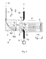
- FIG. 2 shows an enlarged and more detailed view of the spectroscopic apparatus A in Figure 1 .
- a flux 1 of electrons is shown propagating along electron-optical axis 8.
- This flux 1 enters a dispersing device 3 ("electron prism"), where it is dispersed (fanned out) into an energy-resolved (energy-differentiated) array 5 of spectral sub-beams (schematically indicated in Figure 2 using dashed lines).
- This array 5 of sub-beams encounters an adjustable aperture device 7, which comprises:
- a radiation sensor S which is disposed upstream of aperture device 7, i.e. at a side of aperture device 7 facing toward the incoming sub-beam array 5 / distal from detector D.
- sensor S is attached to first plate 7a proximal to first edge 7a', and is thus co-movable with first plate 7a.
- the sensor S is relatively small, e.g. with a sensing area of a few mm 2 , and is, for example, embodied as a photodiode, SSPM or (small) CMOS/CCD sensor.
- the senor S is used to perform localized radiation sensing in a selected region 5b1 of said second portion 5b of the array 5, simultaneous with detection of said first portion 5a by detector D.
- This selected region is, as its name indicates, selectable: for example, by moving blade 7a slightly toward blade 7b in Figure 2 , one could instead use sensor S to inspect a selected region 5b2 - though this might lead to the eclipsing of a small peripheral zone of admitted first portion 5a.
- a sensing result from sensor S is used to adjust a detection result from detector D.
- Cartesian coordinate system depicted at the lower right of Figure 2 is rotated counterclockwise through 90° compared to the coordinate system at the upper left of the Figure because, conventionally, the Z axis indicates the direction of the (local) electron-optical axis 8, which is deflected in dispersing device 3.
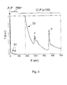
- Figure 3 shows an example of an EELS spectrum.
- the Figure renders intensity I (in arbitrary units, a.u.) as a function of energy-loss E (in eV) for electrons that have traversed a specimen containing Carbon and Titanium. From left to right, the main features of the spectrum are:
Priority Applications (5)
| Application Number | Priority Date | Filing Date | Title |
|---|---|---|---|
| EP14183576.9A EP2993682A1 (fr) | 2014-09-04 | 2014-09-04 | Procédé permettant de réaliser une spectroscopie dans un microscope à particules chargées de transmission |
| EP15183309.2A EP2993683B1 (fr) | 2014-09-04 | 2015-09-01 | Procédé permettant de réaliser une spectroscopie dans un microscope à particules chargées de transmission |
| CN201510554068.9A CN105405734B (zh) | 2014-09-04 | 2015-09-02 | 在透射带电粒子显微镜中执行光谱术的方法 |
| US14/844,778 US9524851B2 (en) | 2014-09-04 | 2015-09-03 | Method of performing spectroscopy in a transmission charged-particle microscope |
| JP2015173596A JP6162187B2 (ja) | 2014-09-04 | 2015-09-03 | 透過型荷電粒子顕微鏡内で分光を実行する方法 |
Applications Claiming Priority (1)
| Application Number | Priority Date | Filing Date | Title |
|---|---|---|---|
| EP14183576.9A EP2993682A1 (fr) | 2014-09-04 | 2014-09-04 | Procédé permettant de réaliser une spectroscopie dans un microscope à particules chargées de transmission |
Publications (1)
| Publication Number | Publication Date |
|---|---|
| EP2993682A1 true EP2993682A1 (fr) | 2016-03-09 |
Family
ID=51454621
Family Applications (2)
| Application Number | Title | Priority Date | Filing Date |
|---|---|---|---|
| EP14183576.9A Withdrawn EP2993682A1 (fr) | 2014-09-04 | 2014-09-04 | Procédé permettant de réaliser une spectroscopie dans un microscope à particules chargées de transmission |
| EP15183309.2A Active EP2993683B1 (fr) | 2014-09-04 | 2015-09-01 | Procédé permettant de réaliser une spectroscopie dans un microscope à particules chargées de transmission |
Family Applications After (1)
| Application Number | Title | Priority Date | Filing Date |
|---|---|---|---|
| EP15183309.2A Active EP2993683B1 (fr) | 2014-09-04 | 2015-09-01 | Procédé permettant de réaliser une spectroscopie dans un microscope à particules chargées de transmission |
Country Status (4)
| Country | Link |
|---|---|
| US (1) | US9524851B2 (fr) |
| EP (2) | EP2993682A1 (fr) |
| JP (1) | JP6162187B2 (fr) |
| CN (1) | CN105405734B (fr) |
Families Citing this family (10)
| Publication number | Priority date | Publication date | Assignee | Title |
|---|---|---|---|---|
| EP3070732A1 (fr) * | 2015-03-18 | 2016-09-21 | Fei Company | Appareil et procédé permettant de réaliser une spectroscopie dans un microscope à particules chargées en transmission |
| US10495516B2 (en) * | 2015-06-30 | 2019-12-03 | Imec Vzw | Dedicated transformation spectroscopy |
| WO2018086853A1 (fr) * | 2016-11-09 | 2018-05-17 | Imec Vzw | Appareil pour tomographie stem et eds combinée |
| EP3444836B1 (fr) * | 2017-08-17 | 2020-01-29 | FEI Company | Détection d'un motif de diffraction dans un microscope à transmission à particules chargées |
| US10522323B2 (en) * | 2018-04-05 | 2019-12-31 | Fei Company | Electron energy loss spectroscopy with adjustable energy resolution |
| EP3564982A1 (fr) * | 2018-05-02 | 2019-11-06 | FEI Company | Technique de détection eels dans un microscope électronique |
| US10699875B2 (en) * | 2018-11-13 | 2020-06-30 | Fei Company | Confocal imaging technique in a charged particle microscope |
| CN111046325B (zh) * | 2019-09-30 | 2021-11-19 | 西安交通大学 | 一种化合物材料电子非弹性散射截面的确定方法 |
| JP2022034866A (ja) * | 2020-08-19 | 2022-03-04 | 株式会社ニューフレアテクノロジー | マルチ電子ビーム検査装置及びその調整方法 |
| US20220404247A1 (en) * | 2021-06-21 | 2022-12-22 | Fei Company | Vibration-free cryogenic cooling |
Citations (3)
| Publication number | Priority date | Publication date | Assignee | Title |
|---|---|---|---|---|
| US7642513B2 (en) | 2004-08-04 | 2010-01-05 | Centre National De La Recherche Scientifique | Device for obtaining the image and/or spectra of electron energy loss |
| EP2387062A1 (fr) * | 2010-05-12 | 2011-11-16 | FEI Company | Détection simultanée d'électrons |
| US8334512B2 (en) * | 2010-08-25 | 2012-12-18 | Fei Company | Detector system for use with transmission electron microscope spectroscopy |
Family Cites Families (13)
| Publication number | Priority date | Publication date | Assignee | Title |
|---|---|---|---|---|
| JPS595869U (ja) * | 1982-07-02 | 1984-01-14 | 日本電子株式会社 | 可変スリツト装置 |
| JPH09330681A (ja) * | 1996-06-07 | 1997-12-22 | Ricoh Co Ltd | 高分解能電子エネルギー損失分光測定装置 |
| JP2000348670A (ja) * | 1999-06-08 | 2000-12-15 | Ricoh Co Ltd | 電子線分光装置および電子顕微鏡 |
| JP2003114204A (ja) * | 2001-10-03 | 2003-04-18 | Canon Inc | 状態検出装置および状態検出方法、走査型分析装置および元素分析方法 |
| JP2004214057A (ja) * | 2003-01-06 | 2004-07-29 | Hitachi High-Technologies Corp | 電子線分光器、それを備えた電子顕微鏡及び分析方法 |
| CN101523171A (zh) * | 2005-07-11 | 2009-09-02 | 瑞沃瑞公司 | 用于非破坏性地确定薄膜中元素的分布轮廓的方法和系统 |
| EP2270834B9 (fr) * | 2005-09-06 | 2013-07-10 | Carl Zeiss SMT GmbH | Composant optique corpusculaire |
| US9153413B2 (en) * | 2007-02-22 | 2015-10-06 | Applied Materials Israel, Ltd. | Multi-beam scanning electron beam device and methods of using the same |
| US20120112091A1 (en) * | 2010-11-04 | 2012-05-10 | National Taiwan University | Method for adjusting status of particle beams for patterning a substrate and system using the same |
| JP5637841B2 (ja) * | 2010-12-27 | 2014-12-10 | 株式会社日立ハイテクノロジーズ | 検査装置 |
| US8704176B2 (en) * | 2011-08-10 | 2014-04-22 | Fei Company | Charged particle microscope providing depth-resolved imagery |
| EP2690431A1 (fr) | 2012-07-23 | 2014-01-29 | FEI Company | Technique de spectroscopie par rayons X utilisant des données spectrales fusionnées |
| EP2824445B1 (fr) | 2013-07-08 | 2016-03-02 | Fei Company | Microscopie à particules chargées combinée avec spectroscopie raman |
-
2014
- 2014-09-04 EP EP14183576.9A patent/EP2993682A1/fr not_active Withdrawn
-
2015
- 2015-09-01 EP EP15183309.2A patent/EP2993683B1/fr active Active
- 2015-09-02 CN CN201510554068.9A patent/CN105405734B/zh active Active
- 2015-09-03 JP JP2015173596A patent/JP6162187B2/ja active Active
- 2015-09-03 US US14/844,778 patent/US9524851B2/en active Active
Patent Citations (3)
| Publication number | Priority date | Publication date | Assignee | Title |
|---|---|---|---|---|
| US7642513B2 (en) | 2004-08-04 | 2010-01-05 | Centre National De La Recherche Scientifique | Device for obtaining the image and/or spectra of electron energy loss |
| EP2387062A1 (fr) * | 2010-05-12 | 2011-11-16 | FEI Company | Détection simultanée d'électrons |
| US8334512B2 (en) * | 2010-08-25 | 2012-12-18 | Fei Company | Detector system for use with transmission electron microscope spectroscopy |
Non-Patent Citations (2)
| Title |
|---|
| RAY EGERTON: "Electron Energy-Loss Spectroscopy in the Electron Microscope", 2011, SPRINGER SCIENCE & BUSINESS MEDIA |
| W.H. ESCOVITZ; T.R. FOX; R. LEVI-SETTI: "Scanning Transmission Ion Microscope with a Field Ion Source", PROC. NAT. ACAD. SCI. USA, vol. 72, no. 5, 1975, pages 1826 - 1828, XP002402529, DOI: doi:10.1073/pnas.72.5.1826 |
Also Published As
| Publication number | Publication date |
|---|---|
| US20160071689A1 (en) | 2016-03-10 |
| JP6162187B2 (ja) | 2017-07-12 |
| CN105405734B (zh) | 2018-03-02 |
| JP2016057294A (ja) | 2016-04-21 |
| EP2993683B1 (fr) | 2017-04-26 |
| CN105405734A (zh) | 2016-03-16 |
| US9524851B2 (en) | 2016-12-20 |
| EP2993683A1 (fr) | 2016-03-09 |
Similar Documents
| Publication | Publication Date | Title |
|---|---|---|
| EP2993683B1 (fr) | Procédé permettant de réaliser une spectroscopie dans un microscope à particules chargées de transmission | |
| US9991087B2 (en) | Spectroscopy in a transmission charged-particle microscope | |
| US9778377B2 (en) | Method of performing spectroscopy in a transmission charged-particle microscope | |
| US10522323B2 (en) | Electron energy loss spectroscopy with adjustable energy resolution | |
| JP2014056820A (ja) | 荷電粒子顕微鏡内において試料の断層撮像を実行する方法 | |
| US10832901B2 (en) | EELS detection technique in an electron microscope | |
| CN108538693B (zh) | 带电粒子显微镜的像差测量 | |
| US11024483B2 (en) | Transmission charged particle microscope with adjustable beam energy spread | |
| JP7105647B2 (ja) | 透過型荷電粒子顕微鏡における回折パターン検出 | |
| US10559448B2 (en) | Transmission charged particle microscope with improved EELS/EFTEM module | |
| CN113848220A (zh) | 使用透射带电粒子显微镜对样本进行成像的方法 | |
| US11948771B2 (en) | Method of determining an energy width of a charged particle beam | |
| US10699875B2 (en) | Confocal imaging technique in a charged particle microscope |
Legal Events
| Date | Code | Title | Description |
|---|---|---|---|
| PUAI | Public reference made under article 153(3) epc to a published international application that has entered the european phase |
Free format text: ORIGINAL CODE: 0009012 |
|
| AK | Designated contracting states |
Kind code of ref document: A1 Designated state(s): AL AT BE BG CH CY CZ DE DK EE ES FI FR GB GR HR HU IE IS IT LI LT LU LV MC MK MT NL NO PL PT RO RS SE SI SK SM TR |
|
| AX | Request for extension of the european patent |
Extension state: BA ME |
|
| STAA | Information on the status of an ep patent application or granted ep patent |
Free format text: STATUS: THE APPLICATION IS DEEMED TO BE WITHDRAWN |
|
| 18D | Application deemed to be withdrawn |
Effective date: 20160910 |