EP2993199A1 - Photoalignment agent and liquid crystal display device - Google Patents
Photoalignment agent and liquid crystal display device Download PDFInfo
- Publication number
- EP2993199A1 EP2993199A1 EP15183564.2A EP15183564A EP2993199A1 EP 2993199 A1 EP2993199 A1 EP 2993199A1 EP 15183564 A EP15183564 A EP 15183564A EP 2993199 A1 EP2993199 A1 EP 2993199A1
- Authority
- EP
- European Patent Office
- Prior art keywords
- chemical formula
- photoalignment
- agent
- layer
- electrode
- Prior art date
- Legal status (The legal status is an assumption and is not a legal conclusion. Google has not performed a legal analysis and makes no representation as to the accuracy of the status listed.)
- Granted
Links
- CWVGVGTUSROAIP-UHFFFAOYSA-N CC(C)(C)[NH+]([O-])OC(C)=C Chemical compound CC(C)(C)[NH+]([O-])OC(C)=C CWVGVGTUSROAIP-UHFFFAOYSA-N 0.000 description 1
- OKRNLSUTBJUVKA-UHFFFAOYSA-N OCCN(CCO)C(CCCCC(N(CCO)CCO)=O)=O Chemical compound OCCN(CCO)C(CCCCC(N(CCO)CCO)=O)=O OKRNLSUTBJUVKA-UHFFFAOYSA-N 0.000 description 1
Images


Classifications
-
- G—PHYSICS
- G02—OPTICS
- G02F—OPTICAL DEVICES OR ARRANGEMENTS FOR THE CONTROL OF LIGHT BY MODIFICATION OF THE OPTICAL PROPERTIES OF THE MEDIA OF THE ELEMENTS INVOLVED THEREIN; NON-LINEAR OPTICS; FREQUENCY-CHANGING OF LIGHT; OPTICAL LOGIC ELEMENTS; OPTICAL ANALOGUE/DIGITAL CONVERTERS
- G02F1/00—Devices or arrangements for the control of the intensity, colour, phase, polarisation or direction of light arriving from an independent light source, e.g. switching, gating or modulating; Non-linear optics
- G02F1/01—Devices or arrangements for the control of the intensity, colour, phase, polarisation or direction of light arriving from an independent light source, e.g. switching, gating or modulating; Non-linear optics for the control of the intensity, phase, polarisation or colour
- G02F1/13—Devices or arrangements for the control of the intensity, colour, phase, polarisation or direction of light arriving from an independent light source, e.g. switching, gating or modulating; Non-linear optics for the control of the intensity, phase, polarisation or colour based on liquid crystals, e.g. single liquid crystal display cells
- G02F1/133—Constructional arrangements; Operation of liquid crystal cells; Circuit arrangements
- G02F1/1333—Constructional arrangements; Manufacturing methods
- G02F1/1337—Surface-induced orientation of the liquid crystal molecules, e.g. by alignment layers
- G02F1/133711—Surface-induced orientation of the liquid crystal molecules, e.g. by alignment layers by organic films, e.g. polymeric films
- G02F1/133723—Polyimide, polyamide-imide
-
- C—CHEMISTRY; METALLURGY
- C08—ORGANIC MACROMOLECULAR COMPOUNDS; THEIR PREPARATION OR CHEMICAL WORKING-UP; COMPOSITIONS BASED THEREON
- C08G—MACROMOLECULAR COMPOUNDS OBTAINED OTHERWISE THAN BY REACTIONS ONLY INVOLVING UNSATURATED CARBON-TO-CARBON BONDS
- C08G73/00—Macromolecular compounds obtained by reactions forming a linkage containing nitrogen with or without oxygen or carbon in the main chain of the macromolecule, not provided for in groups C08G12/00 - C08G71/00
- C08G73/06—Polycondensates having nitrogen-containing heterocyclic rings in the main chain of the macromolecule
- C08G73/10—Polyimides; Polyester-imides; Polyamide-imides; Polyamide acids or similar polyimide precursors
-
- C—CHEMISTRY; METALLURGY
- C08—ORGANIC MACROMOLECULAR COMPOUNDS; THEIR PREPARATION OR CHEMICAL WORKING-UP; COMPOSITIONS BASED THEREON
- C08L—COMPOSITIONS OF MACROMOLECULAR COMPOUNDS
- C08L77/00—Compositions of polyamides obtained by reactions forming a carboxylic amide link in the main chain; Compositions of derivatives of such polymers
-
- C—CHEMISTRY; METALLURGY
- C09—DYES; PAINTS; POLISHES; NATURAL RESINS; ADHESIVES; COMPOSITIONS NOT OTHERWISE PROVIDED FOR; APPLICATIONS OF MATERIALS NOT OTHERWISE PROVIDED FOR
- C09K—MATERIALS FOR MISCELLANEOUS APPLICATIONS, NOT PROVIDED FOR ELSEWHERE
- C09K19/00—Liquid crystal materials
- C09K19/52—Liquid crystal materials characterised by components which are not liquid crystals, e.g. additives with special physical aspect: solvents, solid particles
- C09K19/54—Additives having no specific mesophase characterised by their chemical composition
- C09K19/56—Aligning agents
-
- G—PHYSICS
- G02—OPTICS
- G02F—OPTICAL DEVICES OR ARRANGEMENTS FOR THE CONTROL OF LIGHT BY MODIFICATION OF THE OPTICAL PROPERTIES OF THE MEDIA OF THE ELEMENTS INVOLVED THEREIN; NON-LINEAR OPTICS; FREQUENCY-CHANGING OF LIGHT; OPTICAL LOGIC ELEMENTS; OPTICAL ANALOGUE/DIGITAL CONVERTERS
- G02F1/00—Devices or arrangements for the control of the intensity, colour, phase, polarisation or direction of light arriving from an independent light source, e.g. switching, gating or modulating; Non-linear optics
- G02F1/01—Devices or arrangements for the control of the intensity, colour, phase, polarisation or direction of light arriving from an independent light source, e.g. switching, gating or modulating; Non-linear optics for the control of the intensity, phase, polarisation or colour
- G02F1/13—Devices or arrangements for the control of the intensity, colour, phase, polarisation or direction of light arriving from an independent light source, e.g. switching, gating or modulating; Non-linear optics for the control of the intensity, phase, polarisation or colour based on liquid crystals, e.g. single liquid crystal display cells
- G02F1/133—Constructional arrangements; Operation of liquid crystal cells; Circuit arrangements
- G02F1/1333—Constructional arrangements; Manufacturing methods
- G02F1/133345—Insulating layers
-
- G—PHYSICS
- G02—OPTICS
- G02F—OPTICAL DEVICES OR ARRANGEMENTS FOR THE CONTROL OF LIGHT BY MODIFICATION OF THE OPTICAL PROPERTIES OF THE MEDIA OF THE ELEMENTS INVOLVED THEREIN; NON-LINEAR OPTICS; FREQUENCY-CHANGING OF LIGHT; OPTICAL LOGIC ELEMENTS; OPTICAL ANALOGUE/DIGITAL CONVERTERS
- G02F1/00—Devices or arrangements for the control of the intensity, colour, phase, polarisation or direction of light arriving from an independent light source, e.g. switching, gating or modulating; Non-linear optics
- G02F1/01—Devices or arrangements for the control of the intensity, colour, phase, polarisation or direction of light arriving from an independent light source, e.g. switching, gating or modulating; Non-linear optics for the control of the intensity, phase, polarisation or colour
- G02F1/13—Devices or arrangements for the control of the intensity, colour, phase, polarisation or direction of light arriving from an independent light source, e.g. switching, gating or modulating; Non-linear optics for the control of the intensity, phase, polarisation or colour based on liquid crystals, e.g. single liquid crystal display cells
- G02F1/133—Constructional arrangements; Operation of liquid crystal cells; Circuit arrangements
- G02F1/1333—Constructional arrangements; Manufacturing methods
- G02F1/1337—Surface-induced orientation of the liquid crystal molecules, e.g. by alignment layers
- G02F1/13378—Surface-induced orientation of the liquid crystal molecules, e.g. by alignment layers by treatment of the surface, e.g. embossing, rubbing or light irradiation
- G02F1/133788—Surface-induced orientation of the liquid crystal molecules, e.g. by alignment layers by treatment of the surface, e.g. embossing, rubbing or light irradiation by light irradiation, e.g. linearly polarised light photo-polymerisation
-
- G—PHYSICS
- G02—OPTICS
- G02F—OPTICAL DEVICES OR ARRANGEMENTS FOR THE CONTROL OF LIGHT BY MODIFICATION OF THE OPTICAL PROPERTIES OF THE MEDIA OF THE ELEMENTS INVOLVED THEREIN; NON-LINEAR OPTICS; FREQUENCY-CHANGING OF LIGHT; OPTICAL LOGIC ELEMENTS; OPTICAL ANALOGUE/DIGITAL CONVERTERS
- G02F1/00—Devices or arrangements for the control of the intensity, colour, phase, polarisation or direction of light arriving from an independent light source, e.g. switching, gating or modulating; Non-linear optics
- G02F1/01—Devices or arrangements for the control of the intensity, colour, phase, polarisation or direction of light arriving from an independent light source, e.g. switching, gating or modulating; Non-linear optics for the control of the intensity, phase, polarisation or colour
- G02F1/13—Devices or arrangements for the control of the intensity, colour, phase, polarisation or direction of light arriving from an independent light source, e.g. switching, gating or modulating; Non-linear optics for the control of the intensity, phase, polarisation or colour based on liquid crystals, e.g. single liquid crystal display cells
- G02F1/133—Constructional arrangements; Operation of liquid crystal cells; Circuit arrangements
- G02F1/1333—Constructional arrangements; Manufacturing methods
- G02F1/1343—Electrodes
- G02F1/134309—Electrodes characterised by their geometrical arrangement
-
- G—PHYSICS
- G02—OPTICS
- G02F—OPTICAL DEVICES OR ARRANGEMENTS FOR THE CONTROL OF LIGHT BY MODIFICATION OF THE OPTICAL PROPERTIES OF THE MEDIA OF THE ELEMENTS INVOLVED THEREIN; NON-LINEAR OPTICS; FREQUENCY-CHANGING OF LIGHT; OPTICAL LOGIC ELEMENTS; OPTICAL ANALOGUE/DIGITAL CONVERTERS
- G02F1/00—Devices or arrangements for the control of the intensity, colour, phase, polarisation or direction of light arriving from an independent light source, e.g. switching, gating or modulating; Non-linear optics
- G02F1/01—Devices or arrangements for the control of the intensity, colour, phase, polarisation or direction of light arriving from an independent light source, e.g. switching, gating or modulating; Non-linear optics for the control of the intensity, phase, polarisation or colour
- G02F1/13—Devices or arrangements for the control of the intensity, colour, phase, polarisation or direction of light arriving from an independent light source, e.g. switching, gating or modulating; Non-linear optics for the control of the intensity, phase, polarisation or colour based on liquid crystals, e.g. single liquid crystal display cells
- G02F1/133—Constructional arrangements; Operation of liquid crystal cells; Circuit arrangements
- G02F1/136—Liquid crystal cells structurally associated with a semi-conducting layer or substrate, e.g. cells forming part of an integrated circuit
- G02F1/1362—Active matrix addressed cells
- G02F1/136227—Through-hole connection of the pixel electrode to the active element through an insulation layer
-
- G—PHYSICS
- G02—OPTICS
- G02F—OPTICAL DEVICES OR ARRANGEMENTS FOR THE CONTROL OF LIGHT BY MODIFICATION OF THE OPTICAL PROPERTIES OF THE MEDIA OF THE ELEMENTS INVOLVED THEREIN; NON-LINEAR OPTICS; FREQUENCY-CHANGING OF LIGHT; OPTICAL LOGIC ELEMENTS; OPTICAL ANALOGUE/DIGITAL CONVERTERS
- G02F1/00—Devices or arrangements for the control of the intensity, colour, phase, polarisation or direction of light arriving from an independent light source, e.g. switching, gating or modulating; Non-linear optics
- G02F1/01—Devices or arrangements for the control of the intensity, colour, phase, polarisation or direction of light arriving from an independent light source, e.g. switching, gating or modulating; Non-linear optics for the control of the intensity, phase, polarisation or colour
- G02F1/13—Devices or arrangements for the control of the intensity, colour, phase, polarisation or direction of light arriving from an independent light source, e.g. switching, gating or modulating; Non-linear optics for the control of the intensity, phase, polarisation or colour based on liquid crystals, e.g. single liquid crystal display cells
- G02F1/133—Constructional arrangements; Operation of liquid crystal cells; Circuit arrangements
- G02F1/136—Liquid crystal cells structurally associated with a semi-conducting layer or substrate, e.g. cells forming part of an integrated circuit
- G02F1/1362—Active matrix addressed cells
- G02F1/1368—Active matrix addressed cells in which the switching element is a three-electrode device
-
- C—CHEMISTRY; METALLURGY
- C09—DYES; PAINTS; POLISHES; NATURAL RESINS; ADHESIVES; COMPOSITIONS NOT OTHERWISE PROVIDED FOR; APPLICATIONS OF MATERIALS NOT OTHERWISE PROVIDED FOR
- C09K—MATERIALS FOR MISCELLANEOUS APPLICATIONS, NOT PROVIDED FOR ELSEWHERE
- C09K2323/00—Functional layers of liquid crystal optical display excluding electroactive liquid crystal layer characterised by chemical composition
-
- C—CHEMISTRY; METALLURGY
- C09—DYES; PAINTS; POLISHES; NATURAL RESINS; ADHESIVES; COMPOSITIONS NOT OTHERWISE PROVIDED FOR; APPLICATIONS OF MATERIALS NOT OTHERWISE PROVIDED FOR
- C09K—MATERIALS FOR MISCELLANEOUS APPLICATIONS, NOT PROVIDED FOR ELSEWHERE
- C09K2323/00—Functional layers of liquid crystal optical display excluding electroactive liquid crystal layer characterised by chemical composition
- C09K2323/02—Alignment layer characterised by chemical composition
-
- C—CHEMISTRY; METALLURGY
- C09—DYES; PAINTS; POLISHES; NATURAL RESINS; ADHESIVES; COMPOSITIONS NOT OTHERWISE PROVIDED FOR; APPLICATIONS OF MATERIALS NOT OTHERWISE PROVIDED FOR
- C09K—MATERIALS FOR MISCELLANEOUS APPLICATIONS, NOT PROVIDED FOR ELSEWHERE
- C09K2323/00—Functional layers of liquid crystal optical display excluding electroactive liquid crystal layer characterised by chemical composition
- C09K2323/02—Alignment layer characterised by chemical composition
- C09K2323/025—Polyamide
-
- G—PHYSICS
- G02—OPTICS
- G02F—OPTICAL DEVICES OR ARRANGEMENTS FOR THE CONTROL OF LIGHT BY MODIFICATION OF THE OPTICAL PROPERTIES OF THE MEDIA OF THE ELEMENTS INVOLVED THEREIN; NON-LINEAR OPTICS; FREQUENCY-CHANGING OF LIGHT; OPTICAL LOGIC ELEMENTS; OPTICAL ANALOGUE/DIGITAL CONVERTERS
- G02F1/00—Devices or arrangements for the control of the intensity, colour, phase, polarisation or direction of light arriving from an independent light source, e.g. switching, gating or modulating; Non-linear optics
- G02F1/01—Devices or arrangements for the control of the intensity, colour, phase, polarisation or direction of light arriving from an independent light source, e.g. switching, gating or modulating; Non-linear optics for the control of the intensity, phase, polarisation or colour
- G02F1/13—Devices or arrangements for the control of the intensity, colour, phase, polarisation or direction of light arriving from an independent light source, e.g. switching, gating or modulating; Non-linear optics for the control of the intensity, phase, polarisation or colour based on liquid crystals, e.g. single liquid crystal display cells
- G02F1/133—Constructional arrangements; Operation of liquid crystal cells; Circuit arrangements
- G02F1/1333—Constructional arrangements; Manufacturing methods
- G02F1/133397—Constructional arrangements; Manufacturing methods for suppressing after-image or image-sticking
-
- G—PHYSICS
- G02—OPTICS
- G02F—OPTICAL DEVICES OR ARRANGEMENTS FOR THE CONTROL OF LIGHT BY MODIFICATION OF THE OPTICAL PROPERTIES OF THE MEDIA OF THE ELEMENTS INVOLVED THEREIN; NON-LINEAR OPTICS; FREQUENCY-CHANGING OF LIGHT; OPTICAL LOGIC ELEMENTS; OPTICAL ANALOGUE/DIGITAL CONVERTERS
- G02F1/00—Devices or arrangements for the control of the intensity, colour, phase, polarisation or direction of light arriving from an independent light source, e.g. switching, gating or modulating; Non-linear optics
- G02F1/01—Devices or arrangements for the control of the intensity, colour, phase, polarisation or direction of light arriving from an independent light source, e.g. switching, gating or modulating; Non-linear optics for the control of the intensity, phase, polarisation or colour
- G02F1/13—Devices or arrangements for the control of the intensity, colour, phase, polarisation or direction of light arriving from an independent light source, e.g. switching, gating or modulating; Non-linear optics for the control of the intensity, phase, polarisation or colour based on liquid crystals, e.g. single liquid crystal display cells
- G02F1/133—Constructional arrangements; Operation of liquid crystal cells; Circuit arrangements
- G02F1/1333—Constructional arrangements; Manufacturing methods
- G02F1/1337—Surface-induced orientation of the liquid crystal molecules, e.g. by alignment layers
- G02F1/133711—Surface-induced orientation of the liquid crystal molecules, e.g. by alignment layers by organic films, e.g. polymeric films
Definitions
- the cross-linking agent may be a compound represented by Chemical Formula 1, Chemical Formula 2, or Chemical Formula 3.
- a mole ratio of the first diamine and the second diamine may be in the range of 1:99 to 99:1.
- the mole ratio may be in a range of about 20:80 to 50:50.
- the first diamine comprises an alkylene group (-CH 2- )pertaining to a flexible group, and thus the photoalignment layer formed by using the photoalignment agent containing the copolymer of the first diamine has a flexible characteristic. Accordingly, the anisotropy is improved, thereby ameliorating the afterimage.
- Comparative Example 1 a photoalignment layer in which no cross-linking agent is added into a photoalignment agent including the copolymer of a flexible diamine according to one embodiment of the present invention was used.
- Comparative Example 2 a photoalignment layer in which a rigid cross-linking agent represented by Chemical Formula 4R at 3 wt% is added into the photoalignment agent including the copolymer of the flexible diamine was used.
- Comparative Example 3 a photoalignment layer in which a rigid cross-linking agent represented by Chemical Formula 4R at 3 wt% is added into the photoalignment agent including the copolymer of the flexible diamine was used.
- FIG. 7 illustrates a principle of ameliorating an afterimage in a photoalignment layer formed by using a photoalignment agent added with a flexible cross-linking agent according to the present invention.
- Ohmic contacts 163 and 165 are formed on the semiconductor layer 154.
- the ohmic contacts 163 and 165 may be made of a material such as n+ hydrogenated amorphous silicon in which an n-type impurity such as phosphorus is doped at a high concentration, or of a silicide.
- the ohmic contacts 163 and 165 may be disposed on the semiconductor layer 154 to make a pair. In the case where the semiconductor layer 154 is the oxide semiconductor, the ohmic contacts 163 and 165 may be omitted.
- the data line 171 may have a first curved portion having a curved shape in order to acquire maximum transmittance of the liquid crystal display device, and the curved portion meets itself in a middle region of the pixel area to have a V-lettered shape.
- the liquid crystal display device includes the source electrode 173 positioned on the same line with the data line 171 and the drain electrode 175 extending in parallel with the data line 171, and as a result, a width of the thin film transistor may be increased while an area occupied by the data conductor is not increased, thereby increasing an aperture ratio of the liquid crystal display device.
- the data line 171 and the drain electrode 175 may be made of a refractory metal such as molybdenum, chromium, tantalum, and titanium, or an alloy thereof, and may have a multilayered structure including a refractory metal layer (not illustrated) and a low resistive conductive layer (not illustrated).
- An example of the multilayered structure may include a double layer of a chromium or molybdenum (alloy) lower layer and an aluminum (alloy) upper layer, or a triple layer of a molybdenum (alloy) lower layer, an aluminum (alloy) middle layer, and a molybdenum (alloy) upper layer.
- a first passivation layer 180a is disposed on the data conductors 171, 173, and 175, the gate insulating layer 140, and an exposed portion of the semiconductor layer 154.
- the first passivation layer 180a may be made of an organic insulating material or an inorganic insulating material.
- a photoalignment agent according to an exemplary embodiment of the present invention is coated on the pixel electrode 191, and the coated photoalignment agent is baked.
- the baking may be performed by two steps of pre-baking and hard-baking.
- the polyamic acid included in the photoalignment agent may be converted into a polyimide, and the flexible cross-linking agent may be esterified to be bonded to the polyimide in a range of 150°C to 200°C.
Landscapes
- Physics & Mathematics (AREA)
- Chemical & Material Sciences (AREA)
- Nonlinear Science (AREA)
- Crystallography & Structural Chemistry (AREA)
- Optics & Photonics (AREA)
- General Physics & Mathematics (AREA)
- Mathematical Physics (AREA)
- Organic Chemistry (AREA)
- Polymers & Plastics (AREA)
- Medicinal Chemistry (AREA)
- Chemical Kinetics & Catalysis (AREA)
- Health & Medical Sciences (AREA)
- Engineering & Computer Science (AREA)
- Spectroscopy & Molecular Physics (AREA)
- Microelectronics & Electronic Packaging (AREA)
- Materials Engineering (AREA)
- Geometry (AREA)
- Liquid Crystal (AREA)
- Macromolecular Compounds Obtained By Forming Nitrogen-Containing Linkages In General (AREA)
Abstract
Description
- The present invention relates to a photoalignment agent, a photoalignment layer, a liquid crystal display device, and a manufacturing method thereof.
- In a liquid crystal element, to display images, that is, to switch liquid crystals between sheets of transparent conductive glass through an external electrical field, the liquid crystals must be aligned in a predetermined direction at the interface between the liquid crystals and the transparent conductive glass. The degree of uniformity of the liquid crystal alignment is an important factor for determining the display quality of the liquid crystal display device.
- In a conventional method of aligning the liquid crystals, a rubbing method where a polymer layer such as a polyimide is coated on a substrate such as glass and the surface is rubbed in a predetermined direction by using a fiber material such as nylon or polyester is used. However, minute particles or an electrostatic discharge (ESD) may be generated when the fiber material and the polymer layer are rubbed against each other, and they may cause a serious problem during the manufacturing of the liquid crystal panel.
- To address this, a photoalignment method where anisotropy is induced to the polymer layer by light irradiation to align the liquid crystals has been researched.
- However, there remains a need to provide a photoalignment agent, a photoalignment layer, a liquid crystal display device, and a manufacturing method thereof, having advantages of being capable of optimizing an afterimage and a film strength.
- In one aspect, the present invention provides a photoalignment agent including:
- (a) a copolymer formed from cyclobutanedianhydride (CBDA) or a cyclobutanedianhydride derivative, and a first diamine comprising an alkylene group; and
- (b) a cross-linking agent comprising an alkylene group.
- The first diamine may comprise an alkylene group -CkH2k-, e.g. wherein k is an integer from 1 to 10.
- The cross-linking agent may comprise an alkylene group -CnH2n-, e.g. wherein n is an integer from 1 to 12.
- The cross-linking agent may be a compound represented by Chemical Formula 1, Chemical Formula 2, or Chemical Formula 3.


- In Chemical Formula 1, Chemical Formula 2, and Chemical Formula 3, n is an integer in a range of 3 to 11, each of m1 to m4 are independently an integer in a range of 1 to 4, A1 and A2 are independently


- The cross-linking agent may be a compound that is represented by Chemical Formula 1-1.

- The first diamine may include a compound that is represented by Chemical Formula 4.

- In
Chemical Formula 4, X is -(CH2)h-, -S-(CH2)h-S-, -O-(CH2)h-O-,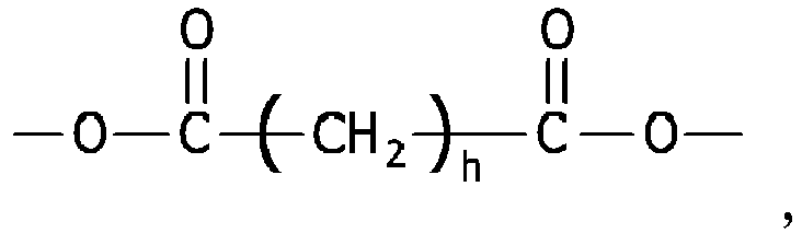


- In preferred embodiment, the copolymer is further formed from a second diamine that is represented by Chemical Formula 5.


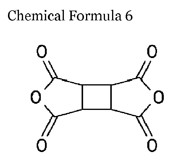
- The cyclobutanedianhydride may be a compound that is represented by Chemical Formula 6, and the cyclobutanedianhydride derivative may be a compound that is represented by Chemical Formula 7.


- The copolymer may include polyamic acid.
- The photoalignment agent may further include at least one solvent selected from N-methyl-2-pyrolidone (NMP) and 2-butyl Cellosolve.
- In a further aspect, the present invention provides a liquid crystal display device comprising: a first substrate; a thin film transistor disposed on the first substrate; a first electrode connected to the thin film transistor; and a first alignment layer disposed on the first electrode. The first alignment layer comprises a photoalignment agent of the present invention.
- In one embodiment, the copolymer comprises at least one repeating unit selected from Chemical Formula 8, Chemical Formula 9, Chemical Formula 10, and Chemical Formula 11.


- In Chemical Formula 8 and Chemical Formula 9, X is -(CH2)h-, -S-(CH2)h-S-, -O-(CH2)h-O-,


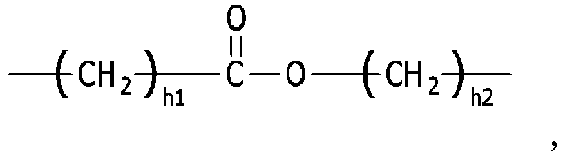
- In one embodiment, h1 and h2 are integers that are selected to obtain 10 as a sum of carbon numbers of the alkylene group of X.
- The copolymer may include a compound that is represented by Chemical Formula 12.

Chemical Formula 12, X is -(CH2)h-, -S-(CH2)h-S-, -O-(CH2)h-O-,


- In one embodiment, h1 and h2 are integers that are selected to obtain 10 as a sum of carbon numbers of the alkylene group of X.
- In a further aspect, the present invention provides a liquid crystal display device comprising: a first substrate; a thin film transistor disposed on the first substrate; a first electrode connected to the thin film transistor; and a first alignment layer disposed on the first electrode. The first alignment layer comprises a photoalignment agent of the present invention.
- The liquid crystal display device may further include a second electrode disposed on the first substrate, wherein an insulating layer is disposed between the first electrode and the second electrode.
- The first electrode may include a plurality of branch electrodes, and the second electrode may have a planar shape.
- The branch electrodes may be overlapped with the second electrode having the planar shape.
- The liquid crystal display device may further comprise a passivation layer positioned between the thin film transistor and the second electrode, wherein the thin film transistor and the first electrode are connected to each other through a contact hole passing through the passivation layer and the insulating layer.
- The liquid crystal display device may further comprise: a second substrate facing the first substrate; a second alignment layer positioned on the second substrate; and a liquid crystal layer positioned between the first substrate and the second substrate and including a liquid crystal molecule, wherein the second alignment layer is formed of the same material as the first alignment layer.
- The present invention provides a photoalignment layer and a liquid crystal display device with optimized afterimage and film strength by using a diamine comprising a flexible group and a cross-linking agent comprising a flexible group to form a photoalignment layer.
- Embodiments of the invention will now be described by way of example with reference to the accompanying drawings, in which:
-
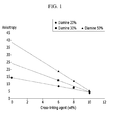
FIG. 1 is a graph illustrating anisotropy according to a flexible diamine content and a flexible cross-linking agent content in a photoalignment layer according to an exemplary embodiment of the present invention; -
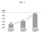
FIG. 2 is a graph illustrating the state of an afterimage in the case of adding a rigid cross-linking agent into a photoalignment layer; -
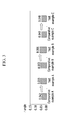
FIG. 3 is a graph illustrating the state of an afterimage in the case of adding a flexible cross-linking agent into a photoalignment layer; -
FIG. 4 is a graph illustrating anisotropy in the case of changing a flexible diamine content and a flexible cross-linking agent content in a photoalignment layer according to an exemplary embodiment of the present invention; -
FIG. 5 is a structural formula illustrating decomposition of the polyimide in a photoalignment layer according to an exemplary embodiment of the present invention; -
FIG. 6 illustrates a change process from isotropic to anisotropic in a photoalignment layer according to an exemplary embodiment of the present invention; -
FIG. 7 illustrates a principle of ameliorating an afterimage in a photoalignment layer formed by using a photoalignment agent added with a flexible cross-linking agent according to an exemplary embodiment of the present invention; -
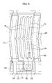
FIG. 8 is a top plan view illustrating a liquid crystal display device according to an exemplary embodiment of the present invention; and -
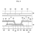
FIG. 9 is cross-sectional view taken along the line IX-IX ofFIG. 8 . - A photoalignment agent according to the present invention comprises (a) a copolymer formed from cyclobutanedianhydride (CBDA) or a cyclobutanedianhydride derivative, and a first diamine comprising an alkylene group, and (b) a cross-linking agent comprising an alkylene group.
- Herein, the cyclobutanedianhydride may be a compound that is represented by Chemical Formula 6, and the cyclobutanedianhydride derivative may be a compound that is represented by Chemical Formula 7.


- In Chemical Formula 7, X1, X2, X3, and X4 are independently hydrogen, a halogen, or an alkyl group, with the proviso that at least one of X1, X2, X3, and X4 is hydrogen. The cyclobutanedianhydride derivative may be a compound that is represented by Chemical Formula 7-1 or Chemical Formula 7-2.


- In one embodiment, the first diamine may be a compound that is represented by Chemical Formula 4.

- In
Chemical Formula 4, X is -(CH2)h-, -S-(CH2)h-S-, -O-(CH2)h-O-,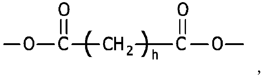


- In one embodiment, the photoalignment agent may further comprise a second diamine that is represented by Chemical Formula 5.

- In addition, the second diamine may be a compound that is represented by Chemical Formula 5, but in which at least one hydrogen attached to the benzene ring is replaced with an alkyl group, a halogen, sulfur, or the like from Chemical Formula 5.
- Suitable second diamine compounds include but are not limited to aromatic diamines such as p-phenylenediamine, m-phenylenediamine, 2,5-diaminotoluene, 2,6-diaminotoluene, 4,4'-diaminobiphenyl, 3,3'-dimethyl-4,4'-diaminobiphenyl, 3,3'-dimethoxy-4,4'-diaminobiphenyl, diaminodiphenylmethane, diaminodiphenylether, 2,2'-diaminodiphenylpropane, bis(3,5-diethyl-4-aminophenyl)methane, diaminodiphenylsulfone, diaminobenzophenone, diaminonaphthalene, 1,4-bis(4-aminophenoxy)benzene, 1,4-bis(4-aminophenyl) benzene, 9,10-bis(4-aminophenyl)anthracene, 1,3-bis(4-aminophenoxy) benzene, 4,4'-bis(4-aminophenoxy)diphenyl sulfone, 2,2-bis[4-(4-minophenoxy)phenyl]propane, 2,2-bis(4-aminophenyl)hexafluoropropane, or 2,2-bis[4-(4-minophenoxy)phenyl]hexafluoropropane; aliphatic diamines such as bis(4-aminocyclohexyl)methane or bis(4-amino-3-methylcyclohexyl)methane; and aliphatic diamines such as tetramethylene diamine or hexamethylenediamine. However, the second diamine is not limited thereto, and may include most kinds of diamines which are not easily bendable excluding the first diamine.
- In one embodiment, a mole ratio of the first diamine and the second diamine may be in the range of 1:99 to 99:1. For example, the mole ratio may be in a range of about 20:80 to 50:50.
- As such, the first diamine comprises an alkylene group (-CH2-)pertaining to a flexible group, and thus the photoalignment layer formed by using the photoalignment agent containing the copolymer of the first diamine has a flexible characteristic. Accordingly, the anisotropy is improved, thereby ameliorating the afterimage.
- In one embodiment, the cross-linking agent may be at least one compound represented by Chemical Formula 1, Chemical Formula 2, or Chemical Formula 3.


- In Chemical Formula 1, Chemical Formula 2, and Chemical Formula 3, n is an integer in a range of 3 to 11, and each of m1 to m4 are independently integers in a range of 1 to 4.
- In
Chemical Formula 1,Chemical Formula 2, andChemical Formula 3, A1 and A2 are independently

- In
Chemical Formula 1,Chemical Formula 2, andChemical Formula 3, each of X1, X2, X3, X4, X5, X6, X7, X8, X9, and X10 are independently -OH, -NH2, an aryl group, a vinyl group, or
- In one embodiment, the cross-linking agent may be included in the photoalignment agent at about 3 wt% to 10 wt% with respect to all contents. For example, the cross-linking agent may be included in the photoalignment agent at about 5 wt% to 7 wt%.
- In one embodiment, the cross-linking agent is a compound that is represented by Chemical Formula 1-1.

- As described above, the cross-linking agent according to the present exemplary embodiment includes the alkylene group (-CH2-)pertaining to the flexible group, and thus the photoalignment layer formed by using the photoalignment agent added with the cross-linking agent ameliorates the film strength and minimizes deterioration of the afterimage.
- Hereinafter, an example of a manufacturing method of a photoalignment agent will be described.
- A compound represented by
Chemical Formula 4 at 0.5 moles and N-methyl-2-pyrolidone were mixed in a flask with four necks and including an agitator, a temperature adjuster, a gas injector, and a cooler, under a dark room condition while passing nitrogen through the flask, to produce a mixed solution. A compound represented byChemical Formula 7 at 1.0 mole was added into the mixed solution, and was subjected to agitation for about one hour. Then, a compound represented byChemical Formula 5 at 0.5 moles was added thereinto to facilitate a reaction. In this case, the reaction was performed for about 24 hours while maintaining the temperature in a range of 30 to 60°C, thereby producing a polyamic acid solution. This polyamic acid solution was distillated to obtain polyamic acid. The weight average molecular weight of the polyamic acid was in a range of 3 to 50,000. A mixed solvent (volume ratio = about 7:2) in which N-methyl-2-pyrolidone (NMP) and 2-butyl cellosolve were mixed was added to the polyamic acid, and was subjected to agitation for 24 hours. A cross-linking agent represented by Chemical Formula 1-1 at about 5 wt% to 7 wt% was added into the mixed solvent, thereby producing a photoalignment agent including the polyamic acid and the cross-linking agent.


- In
Chemical Formula 7, X1 and X4 indicate a methyl group, and X2 and X3 indicate hydrogen.

- The aforementioned photoalignment agent was coated on an electrode, and the coated photoalignment agent was baked. The baking was performed by two steps of pre-baking and hard-baking.
- Thereafter, the first photoalignment layer may be formed by irradiating polarized light to the photoalignment agent. In this case, the irradiated light may be ultraviolet light having a wavelength range of 240 nanometers to 380 nanometers. Preferably, the ultraviolet light with a wavelength of 254 nanometers may be used. The polarized light may have energy in a range of 0.20 J/cm2 to 1.0 J/cm2. For example, the polarized light may have energy in a range of 0.40 J/cm2 to 0.50 J/cm2.
- In order to increase an alignment property, the
photoalignment layer 11 may be baked once more. - In one embodiment, the polymer included in the photoalignment layer comprises at least one repeating unit represented by Chemical Formula 8, Chemical Formula 9,
Chemical Formula 10, andChemical Formula 11.

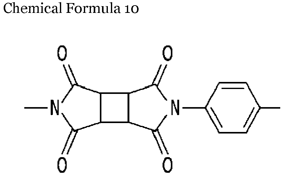
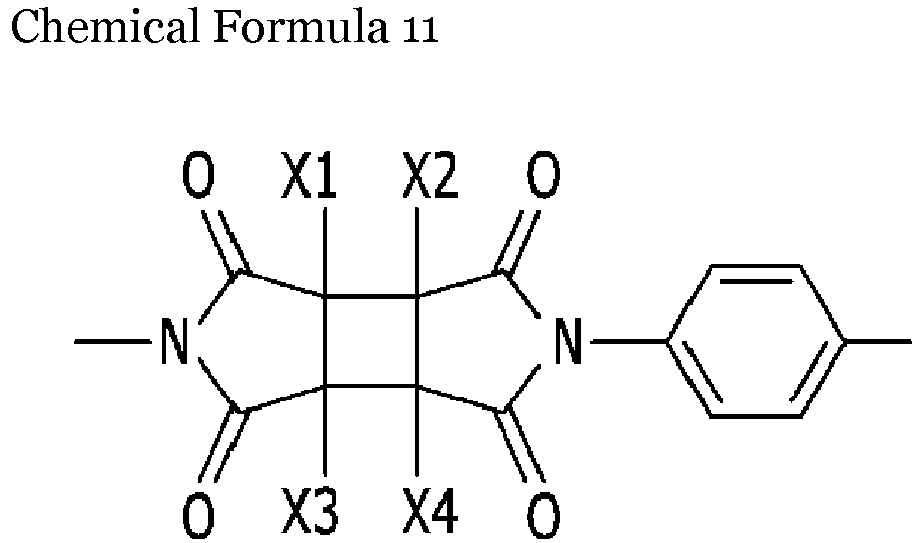


Chemical Formula 11, X1, X2, X3, and X4 are independently hydrogen, a halogen, or an alkyl group, with the proviso that at least one of X1, X2, X3, and X4 is hydrogen. - For example, the photoalignment layer may comprise a copolymer represented by
Chemical Formula 12.
- In
Chemical Formula 12, X is -(CH2)h-, -S-(CH2)h-S-, -O-(CH2)h-O-,


-
FIG. 1 is a graph illustrating anisotropy according to a flexible diamine content and a flexible cross-linking agent content in a photoalignment layer according to the present invention. - Referring to
FIG. 1 , as the flexible diamine content is increased, the anisotropy may also be increased, thereby ameliorating the afterimage. However, the film strength of the photoalignment layer may be deteriorated. In general, when the rigid cross-linking agent is added into the photoalignment layer, the film strength is improved. However, when the rigid cross-linking agent is added, the afterimage may be deteriorated. -
FIG. 2 is a graph illustrating the state of an afterimage in the case of adding a rigid cross-linking agent into a photoalignment layer. - In
FIG. 2 , in Comparative Example 1, a photoalignment layer in which no cross-linking agent is added into a photoalignment agent including the copolymer of a flexible diamine according to one embodiment of the present invention was used. In Comparative Example 2, a photoalignment layer in which a rigid cross-linking agent represented by Chemical Formula 4R at 3 wt% is added into the photoalignment agent including the copolymer of the flexible diamine was used. In Comparative Example 3, a photoalignment layer in which a rigid cross-linking agent represented by Chemical Formula 4R at 3 wt% is added into the photoalignment agent including the copolymer of the flexible diamine was used. Commonly, Comparative Example 1, Comparative Example 2, and Comparative Example 3 were subjected to a first baking process at a temperature of 210°C for about 30 minutes, and then to polarization irradiation at 0.5 J/cm2. Then, a second baking process was performed thereon at the temperature of 210°C for about 30 minutes.
- In Chemical Formula 4R, X may indicate

- Referring to
FIG. 2 , as more rigid cross-linking agent is added, the afterimage is gradually deteriorated. Accordingly, this rigid cross-linking agent is not appropriate for the photoalignment layer formed by using the flexible diamine as a cross-linking agent for improving the film strength. -
FIG. 3 is a graph illustrating the state of an afterimage in the case of adding a flexible cross-linking agent into a photoalignment layer. - In
FIG. 3 , in Comparative Example A, Comparative Example B, and Comparative Example C, photoalignment layers having no cross-linking agent were used. In Test Example A, Test Example B, and Test Example C, photoalignment layers in which a flexible cross-linking agent was added at 3 wt% were used. Comparative Example A and Test Example A were commonly subjected to the first baking process at atemperature 230°C for about 900 seconds, and then to the polarization irradiation at 0.5 J/cm2. Subsequently, the second baking process was performed thereon at a temperature of 210°C for about 900 seconds. Comparative Example B and Test Example B were commonly subjected to the first baking process at thetemperature 230°C for about 900 seconds, and then to the polarization irradiation at 0.5 J/cm2. Subsequently, the second baking process was performed thereon at the temperature of 230°C for about 900 seconds. Comparative Example C and Test Example C were commonly subjected to the first baking process at a temperature 240°C for about 900 seconds, and then to the polarization irradiation of 0.5 J/cm2. Subsequently, the second baking process was performed thereon at the temperature of 210°C for about 900 seconds. - Referring to
FIG. 3 , the afterimage was not deteriorated or was slightly deteriorated in Test Examples A, B, and C adding the flexible cross-linking agent, as compared with Comparative Examples A, B, and C. -
FIG. 4 is a graph illustrating anisotropy in the case of changing a flexible diamine content and a flexible cross-linking agent content in a photoalignment layer according to an exemplary embodiment of the present invention. - Referring to
FIG. 4 , the anisotropy may be reduced to deteriorate the afterimage by adding a flexible cross-linking agent according to one embodiment of the present invention as compared with the case of adding no flexible cross-linking agent. However, in the present embodiment, a photoalignment layer is formed by using a flexible diamine, and thus the reduction of anisotropy caused by adding the flexible cross-linking agent can be sufficiently compensated, or the anisotropy can be increased by more than the reduction. InFIG. 4 , for example,D5 20 % indicates a mole ratio of a mixed flexible diamine as compared with a rigid diamine. - Hereinafter, a principle of improving the film strength and minimizing deterioration of the afterimage when a flexible cross-linking agent according to the present invention is used will be described with reference to
FIG. 5 to FIG. 7 . -
FIG. 5 is a structural formula illustrating decomposition of the polyimide in a photoalignment layer according to the present invention.FIG. 6 illustrates a change process from isotropic to anisotropic in a photoalignment layer according to the present invention. - Referring to
FIG. 5 , a polyamic acid is formed by copolymerizing cyclobutanedianhydride (CBDA) and the diamine. Through a baking process, a polyimide (Unit 1) is formed, and UV is radiated on the polyimide to form a maleimide (Unit 1'). -
FIG. 6 illustrates that a polymer main chain including the polyimide (unit 1) illustrated inFIG. 5 is decomposed to be aligned according to radiation of polarized UV. Referring toFIG. 6 , polarized UV is radiated on an isotropic polymer main chain, photodecomposition occurs in a polarization direction (absorption axis direction), and thus a photoalignment layer may be aligned in a direction that is perpendicular to the polarization. Herein, if an exposure amount is excessively small, since decomposition efficiency is low, the alignment property may deteriorate. On the contrary, if the exposure amount is excessively increased, since decomposition efficiency is increased, decomposition occurs in another direction in addition to the polarization direction, and thus the alignment property may deteriorate. -
FIG. 7 illustrates a principle of ameliorating an afterimage in a photoalignment layer formed by using a photoalignment agent added with a flexible cross-linking agent according to the present invention. - Referring to
FIG. 7 , when the second bake process is performed on the photoalignment layer including the rigid cross-linking agent, the rigid cross-linking agent obstructs the rearrangement of the photo-decomposed molecules. As a result, it is difficult to accomplish a high effect of ameliorating the afterimage with the rearrangement. However, as in the present exemplary embodiment, when the photoalignment layer including the flexible cross-linking agent is subjected to the second baking process, the photo-decomposed molecules can be more easily rearranged, thereby increasing the effect of ameliorating the afterimage with the rearrangement. - Hereinafter, a liquid crystal display device including a photoalignment layer according to the present invention will be described.
-
FIG. 8 is a top plan view illustrating a liquid crystal display device according to an embodiment of the present invention.FIG. 9 is a cross-sectional view taken along the line IX-IX ofFIG. 8 . - Referring to
FIG. 8 andFIG. 9 , the liquid crystal display device includes alower display panel 100 and anupper display panel 200 facing each other, and aliquid crystal layer 3 injected therebetween. - First, the
lower display panel 100 will be described. - A gate conductor including a
gate line 121 is formed on afirst substrate 110 made of transparent glass, plastic, or the like. - The
gate line 121 includes agate electrode 124 and a wide end portion (not illustrated) for connection with another layer or an external driving circuit. Thegate line 121 may be made of an aluminum-based metal such as aluminum (Al) or an aluminum alloy, a silver-based metal such as silver (Ag) or a silver alloy, a copper-based metal such as copper (Cu) or a copper alloy, a molybdenum-based metal such as molybdenum (Mo) or a molybdenum alloy, chromium (Cr), tantalum (Ta), and titanium (Ti). However, thegate line 121 may have a multilayer structure including at least two conductive layers having different physical properties. - A
gate insulating layer 140 made of a silicon nitride (SiNx), a silicon oxide (SiOx), or the like is formed on thegate line 121. Thegate insulating layer 140 may have a multilayer structure including at least two insulating layers having different physical properties. - A
semiconductor layer 154 made of amorphous silicon or polysilicon is positioned on thegate insulating layer 140. Thesemiconductor layer 154 may include an oxide semiconductor. -
Ohmic contacts semiconductor layer 154. Theohmic contacts ohmic contacts semiconductor layer 154 to make a pair. In the case where thesemiconductor layer 154 is the oxide semiconductor, theohmic contacts - A data conductor including a
data line 171 including asource electrode 173 and adrain electrode 175 is formed on theohmic contacts gate insulating layer 140. - The
data line 171 includes a wide end portion (not illustrated) for connection with another layer or an external driving circuit. Thedata line 171 transfers a data signal and mainly extends in a vertical direction to cross thegate line 121. - In this case, the
data line 171 may have a first curved portion having a curved shape in order to acquire maximum transmittance of the liquid crystal display device, and the curved portion meets itself in a middle region of the pixel area to have a V-lettered shape. - The
source electrode 173 is a part of thedata line 171, and is disposed on the same line as thedata line 171. Thedrain electrode 175 is formed to extend in parallel with thesource electrode 173. Accordingly, thedrain electrode 175 is parallel with the part of thedata line 171. - The
gate electrode 124, thesource electrode 173, and thedrain electrode 175 form one thin film transistor (TFT) together with thesemiconductor layer 154, and a channel of the thin film transistor is formed in thesemiconductor layer 154 portion between thesource electrode 173 and thedrain electrode 175. - The liquid crystal display device includes the
source electrode 173 positioned on the same line with thedata line 171 and thedrain electrode 175 extending in parallel with thedata line 171, and as a result, a width of the thin film transistor may be increased while an area occupied by the data conductor is not increased, thereby increasing an aperture ratio of the liquid crystal display device. - The
data line 171 and thedrain electrode 175 may be made of a refractory metal such as molybdenum, chromium, tantalum, and titanium, or an alloy thereof, and may have a multilayered structure including a refractory metal layer (not illustrated) and a low resistive conductive layer (not illustrated). An example of the multilayered structure may include a double layer of a chromium or molybdenum (alloy) lower layer and an aluminum (alloy) upper layer, or a triple layer of a molybdenum (alloy) lower layer, an aluminum (alloy) middle layer, and a molybdenum (alloy) upper layer. - A
first passivation layer 180a is disposed on thedata conductors gate insulating layer 140, and an exposed portion of thesemiconductor layer 154. Thefirst passivation layer 180a may be made of an organic insulating material or an inorganic insulating material. - A
second passivation layer 180b is formed on thefirst passivation layer 180a. Thesecond passivation layer 180b may be made of an organic insulating material. - The
second passivation layer 180b may be a color filter. In the case where thesecond passivation layer 180b is the color filter, thesecond passivation layer 180b may uniquely display one of primary colors, and an example of the primary colors may include three primary colors such as red, green, and blue, or yellow, cyan, and magenta, and the like. Although not illustrated, the color filter may further include a color filter displaying a mixed color of the primary colors or white other than the primary colors. In the case where thesecond passivation layer 180b is the color filter, thecolor filter 230 may be omitted in theupper display panel 200 to be described below. Unlike in the present exemplary embodiment, thesecond passivation layer 180b may be formed by using an organic insulating material, and a color filter (not shown) may be formed between thefirst passivation layer 180a and thesecond passivation layer 180b. - A
common electrode 270 is formed on thesecond passivation layer 180b. Thecommon electrode 270 has a planar shape and may be formed on the entire surface of thesubstrate 110 as a whole plate, and has anopening 138 disposed in a region corresponding to a periphery of thedrain electrode 175. That is, thecommon electrode 270 may have the planar shape as the plate shape. -
Common electrodes 270 positioned at adjacent pixels are connected to each other to receive a common voltage having a predetermined magnitude supplied from outside of a display area. - An insulating
layer 180c is positioned on thecommon electrode 270. The insulatinglayer 180c may be made of an organic insulating material, an inorganic insulating material, or the like. - A
pixel electrode 191 is positioned on the insulatinglayer 180c. Thepixel electrode 191 includes a curved edge which is substantially parallel with the curved portion of thedata line 171. Thepixel electrode 191 has a plurality ofcutouts 91, and includes a plurality ofbranch electrodes 192 positioned between theadjacent cutouts 91. - The
pixel electrode 191 is a first field generating electrode or a first electrode, and thecommon electrode 270 is a second field generating electrode or a second electrode. A horizontal electric field (ex, fringe field) may be generated between thepixel electrode 191 and thecommon electrode 270. - A
first contact hole 185 exposing thedrain electrode 175 is formed in thefirst passivation layer 180a, thesecond passivation layer 180b, and the insulatinglayer 180c. Thepixel electrode 191 is physically and electrically connected to thedrain electrode 175 through thecontact hole 185 to receive a voltage from thedrain electrode 175. - A
first alignment layer 11 is formed on thepixel electrode 191 and the insulatinglayer 180c. Thefirst alignment layer 11 includes a photoreactive material. - In the present exemplary embodiment, the
first alignment layer 11 includes the photoalignment layer according to the aforementioned exemplary embodiment of the present invention. - Herein, a method of forming the alignment layer will be described.
- A photoalignment agent according to an exemplary embodiment of the present invention is coated on the
pixel electrode 191, and the coated photoalignment agent is baked. The baking may be performed by two steps of pre-baking and hard-baking. In the hard-baking, the polyamic acid included in the photoalignment agent may be converted into a polyimide, and the flexible cross-linking agent may be esterified to be bonded to the polyimide in a range of 150°C to 200°C. - Thereafter, the
first alignment layer 11 may be formed by irradiating polarized light to the photoalignment agent. In this case, the irradiated light may be ultraviolet light having a wavelength range of 240 nanometers to 380 nanometers. Preferably, the ultraviolet light with a wavelength of 254 nanometers may be used. The polarized light may have energy in a range of 0.20 J/cm2 to 1.0 J/cm2. For example, the polarized light may have energy in a range of 0.40 J/cm2 to 0.50 J/cm2. - In order to increase an alignment property, the
first alignment layer 11 may be baked once more. In this case, the photo-decomposed molecules may be rearranged to increase the anisotropy. - Next, the
upper display panel 200 will be described. - A
light blocking member 220 is formed on asecond substrate 210 made of transparent glass or plastic. Thelight blocking member 220 is called a black matrix and blocks light leakage. - A plurality of
color filters 230 are formed on thesecond substrate 210. In the case where thesecond passivation layer 180b of thelower display panel 100 is a color filter or where a color filter is formed on thelower display panel 100, thecolor filter 230 of theupper display panel 200 may be omitted. Further, thelight blocking member 220 of theupper display panel 200 may also be formed on thelower display panel 100. - An
overcoat 250 is formed on thecolor filter 230 and thelight blocking member 220. Theovercoat 250 may be made of an (organic) insulating material, prevents thecolor filter 230 from being exposed, and provides a flat surface. Theovercoat 250 may be omitted. - A
second alignment layer 21 is formed on theovercoat 250. Thesecond alignment layer 21 may be formed by the same material and the same method as thefirst alignment layer 11 described above. - The
liquid crystal layer 3 may include a liquid crystal material having negative or positive dielectric anisotropy. - The liquid crystal molecules of the
liquid crystal layer 3 are aligned so that long axes thereof are parallel to thepanels - The
pixel electrode 191 receives a data voltage from thedrain electrode 175, and thecommon electrode 270 receives a common voltage having a predetermined magnitude from a common voltage applying unit disposed outside of the display area. - The
pixel electrode 191 and thecommon electrode 270 serving as field-generating electrodes generate an electric field, and thus the liquid crystal molecules of theliquid crystal layer 3 positioned on the two field-generatingelectrodes - As such, the two
field generating electrodes display panel 100, thereby increasing transmittance of the liquid crystal display device and implementing a wide viewing angle. - In the liquid crystal display device according to the illustrated exemplary embodiment, the
common electrode 270 has a planar shape, and thepixel electrode 191 has a plurality of branch electrodes, but in a liquid crystal display device according to another exemplary embodiment of the present invention, thepixel electrode 191 may have a planar shape, and thecommon electrode 270 may have a plurality of branch electrodes. - The present invention may be applied to all other cases where the two field generating electrodes are overlapped with each other on the
first substrate 110 with an insulating layer therebetween, the first field generating electrode formed below the insulating layer has a planar shape, and the second field generating electrode formed on the insulating layer has a plurality of branch electrodes. - Although certain exemplary embodiments and implementations have been described herein, other embodiments and modifications will be apparent from this description. Accordingly, the inventive concept is not limited to such embodiments, but rather to the broader scope of the presented claims and various obvious modifications and equivalent arrangements.
Claims (12)
- A photoalignment agent, comprising:(a) a copolymer formed from cyclobutanedianhydride or a cyclobutanedianhydride derivative, and a first diamine comprising an alkylene group; and(b) a cross-linking agent comprising an alkylene group.
- The photoalignment agent of claim 1, wherein the cross-linking agent is a compound represented by Chemical Formula 1, Chemical Formula 2, or Chemical Formula 3:


 n is an integer from 3 to 11;m1 to m4 are independently integers from 1 to 4;A1 and A2 are independently
 R is H, an alkyl group with a carbon number of 1 to 3, an aromatic compound with a carbon number of 6 to 30, or an aliphatic cyclic compound with a carbon number of 4 to 20A3 is
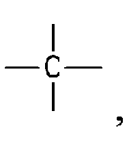 A4 is a single bond, -CH2-, -COO-, -OCO-, -S-, -O-, an aromatic compound with a carbon number of 6 to 30, or an aliphatic cyclic compound with a carbon number of 4 to 20); andeach of X1, X2, X3, X4, X5, X6, X7, X8, X9, and X10 are independently -OH, -NH2, an aryl group, a vinyl group, or
- The photoalignment agent of claim 1, wherein the cross-linking agent is a compound represented by Chemical Formula 1-1:

- The photoalignment agent of any one of the preceding claims, wherein the first diamine is a compound represented by Chemical Formula 4:
 X indicates -(CH2)h-, -S-(CH2)h-S-, -O-(CH2)h-O-,


 h is an integer from 1 to 10; andh1 and h2 are integers selected to obtain a range of 2 to 10 as a sum of carbon numbers of the alkylene group of X.
 - The photoalignment agent of any one of the preceding claims, wherein the copolymer is further formed from a second diamine represented by Chemical Formula 5:
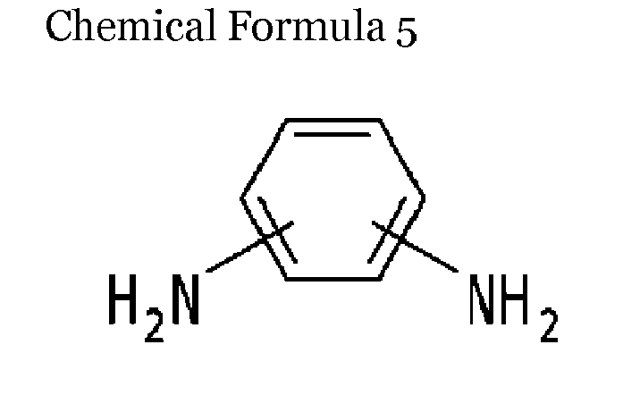
- The photoalignment agent of any one of the preceding claims, wherein the cyclobutanedianhydride is a compound represented by Chemical Formula 6, or the cyclobutanedianhydride derivative is a compound represented by Chemical Formula 7:

 X1, X2, X3, and X4 are independently hydrogen, a halogen, or an alkyl group; with the proviso that at least one of X1, X2, X3, and X4 is not hydrogen.
 - The photoalignment agent of any one of the preceding claims, wherein the copolymer includes polyamic acid.
- The photoalignment agent of any one of the preceding claims, wherein the copolymer comprises at least one repeating unit selected from Chemical Formula 8, Chemical Formula 9, Chemical Formula 10, and Chemical Formula 11:


h1 and h2 are integers selected to obtain a range of 2 to 10 as the sum of carbon numbers of the alkylene group of X; and
X1, X2, X3, and X4 are independently hydrogen, a halogen, or an alkyl group, with the proviso that at least one of X1, X2, X3, and X4 is hydrogen. - The photoalignment agent of any one of the preceding claims, wherein the copolymer comprises the repeating units represented by Chemical Formula 12:

 X indicates -(CH2)h-, -S-(CH2)h-S-, -O-(CH2)h-O-,


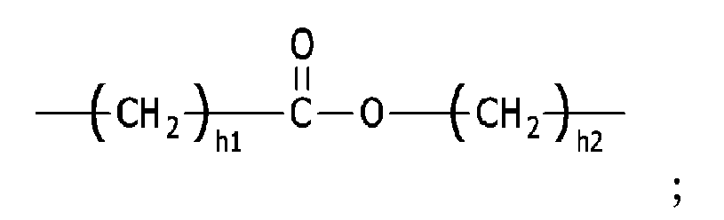 h is an integer from 1 to 10;h1 and h2 are integers selected to obtain a range of 2 to 10 as the sum of carbon numbers of the alkylene group of X;a:b is from 20:80 to 50:50; andX1, X2, X3, and X4 are independently hydrogen, a halogen, or an alkyl group, with the proviso that at least one of X1, X2, X3, and X4 is not hydrogen.
 - The photoalignment agent of any one of the preceding claims, wherein the copolymer comprises a polyimide.
- A liquid crystal display device, comprising:a first substrate;a thin film transistor disposed on the first substrate;a first electrode connected to the thin film transistor; anda first alignment layer disposed on the first electrode,
wherein the first alignment layer comprises a photoalignment agent as defined in any one of the preceding claims. - The liquid crystal display device of claim 11, further comprising:a second electrode disposed on the first substrate,wherein an insulating layer is disposed between the first electrode and the second electrode.
Applications Claiming Priority (1)
| Application Number | Priority Date | Filing Date | Title |
|---|---|---|---|
| KR1020140117938A KR20160029234A (en) | 2014-09-04 | 2014-09-04 | Photo alignment agent, photo alignment film, liquid crystal display device and method of manufacturing the same |
Publications (2)
| Publication Number | Publication Date |
|---|---|
| EP2993199A1 true EP2993199A1 (en) | 2016-03-09 |
| EP2993199B1 EP2993199B1 (en) | 2016-09-28 |
Family
ID=54146938
Family Applications (1)
| Application Number | Title | Priority Date | Filing Date |
|---|---|---|---|
| EP15183564.2A Active EP2993199B1 (en) | 2014-09-04 | 2015-09-02 | Photoalignment agent and liquid crystal display device |
Country Status (5)
| Country | Link |
|---|---|
| US (1) | US10061160B2 (en) |
| EP (1) | EP2993199B1 (en) |
| JP (1) | JP2016057620A (en) |
| KR (1) | KR20160029234A (en) |
| CN (1) | CN105400524B (en) |
Families Citing this family (4)
| Publication number | Priority date | Publication date | Assignee | Title |
|---|---|---|---|---|
| KR102227960B1 (en) * | 2014-10-21 | 2021-03-15 | 삼성디스플레이 주식회사 | Photo alignment agent, photo alignment film, liquid crystal display device and method of manufacturing the same |
| KR102581446B1 (en) * | 2016-04-05 | 2023-09-21 | 삼성디스플레이 주식회사 | Alignment film composition, liquid crystal display device and manufacturing method of the liquid crystal display device |
| KR102621459B1 (en) * | 2016-04-20 | 2024-01-05 | 삼성디스플레이 주식회사 | Composition for alignment layer and liquid crystal display comprising the same and method for manufacturing the liquid crystal display |
| KR102161218B1 (en) * | 2017-09-29 | 2020-09-29 | 주식회사 엘지화학 | Copolymer for liquid crystal aligning agent, liquid crystal aligning agent comprising the same, liquid crystal aligning film, and liquid crystal display device using the same |
Citations (4)
| Publication number | Priority date | Publication date | Assignee | Title |
|---|---|---|---|---|
| WO2008153287A1 (en) * | 2007-06-13 | 2008-12-18 | Korea Research Institute Of Chemical Technology | Low temperature processable substituted alicyclic polyimide photo-alignment layers and method for preparing liquid crystal cells |
| WO2012176822A1 (en) * | 2011-06-21 | 2012-12-27 | 日産化学工業株式会社 | Liquid crystal orientation agent for photo-orientation treatment method and liquid crystal orientation film using same |
| WO2013094734A1 (en) * | 2011-12-22 | 2013-06-27 | 日産化学工業株式会社 | Method for manufacturing liquid-crystal display element for use with in-plane switching |
| US20140072730A1 (en) * | 2012-09-07 | 2014-03-13 | Lg Chem, Ltd. | Photoalignment Polyimide Copolymer and Liquid Crystal Alignment Layer |
Family Cites Families (20)
| Publication number | Priority date | Publication date | Assignee | Title |
|---|---|---|---|---|
| EP0919851B1 (en) | 1996-03-05 | 2003-10-22 | Nissan Chemical Industries, Limited | Method for liquid crystal alignment |
| EP1386910A1 (en) | 2002-07-30 | 2004-02-04 | Rolic AG | Photoactive materials |
| JP4816859B2 (en) * | 2004-02-24 | 2011-11-16 | Jsr株式会社 | Liquid crystal alignment agent |
| TWI360680B (en) * | 2004-02-24 | 2012-03-21 | Jsr Corp | Liquid crystal alignment agent and manufacturing m |
| JP2007121991A (en) | 2005-09-29 | 2007-05-17 | Sony Corp | Liquid crystal orientated film and liquid crystal display element |
| JP5061709B2 (en) | 2006-06-29 | 2012-10-31 | Jnc株式会社 | Composition for liquid crystal alignment film, liquid crystal alignment film, and liquid crystal display element |
| JP4941647B2 (en) | 2006-11-07 | 2012-05-30 | 日産化学工業株式会社 | Resin composition for forming a liquid crystal alignment layer |
| JP4507024B2 (en) | 2007-10-24 | 2010-07-21 | Jsr株式会社 | Liquid crystal aligning agent, method for forming liquid crystal aligning film, and liquid crystal display element |
| JP5354161B2 (en) | 2008-10-17 | 2013-11-27 | Jsr株式会社 | Liquid crystal aligning agent and liquid crystal display element |
| US9052549B2 (en) * | 2008-11-27 | 2015-06-09 | Samsung Display Co., Ltd. | Liquid crystal display and manufacturing method thereof |
| TWI393732B (en) | 2009-03-31 | 2013-04-21 | Daxin Materials Corp | Liquid crystal alignment solution |
| JP5527538B2 (en) | 2009-10-06 | 2014-06-18 | Jsr株式会社 | Liquid crystal aligning agent, method for producing liquid crystal aligning film, and liquid crystal display element |
| KR101288571B1 (en) | 2009-12-22 | 2013-07-22 | 제일모직주식회사 | Liquid crystal photo-alignment agent, liquid crystal photo-alignment film manufactured using the same, and liquid crystal display device including the liquid crystal photo-alignment film |
| CN102712741B (en) | 2010-01-26 | 2014-05-14 | 日产化学工业株式会社 | Curable long-chain alkylene-containing epoxy resin composition |
| JP5569095B2 (en) | 2010-03-29 | 2014-08-13 | Jnc株式会社 | Diamine having diphenylamine structure at two positions in the molecule, polymer obtained by reacting this diamine, liquid crystal aligning agent containing this polymer, liquid crystal aligning film formed using this liquid crystal aligning agent, and this liquid crystal aligning film Liquid crystal display device having |
| JP5771948B2 (en) | 2010-10-28 | 2015-09-02 | 日産化学工業株式会社 | Liquid crystal aligning agent, liquid crystal aligning film, and liquid crystal display element |
| JP2012155311A (en) * | 2011-01-05 | 2012-08-16 | Jnc Corp | Liquid crystal aligning agent for forming photo-aligning liquid crystal alignment layer, liquid crystal alignment layer and liquid crystal display element using the same |
| JP6056187B2 (en) * | 2012-05-09 | 2017-01-11 | Jnc株式会社 | Liquid crystal alignment agent, liquid crystal alignment film for forming liquid crystal alignment film for photo-alignment, and liquid crystal display element using the same |
| KR101985259B1 (en) * | 2012-08-10 | 2019-06-03 | 제이에스알 가부시끼가이샤 | Liquid crystal aligning agent and compound |
| WO2015072554A1 (en) * | 2013-11-15 | 2015-05-21 | 日産化学工業株式会社 | Liquid crystal aligning agent, and liquid crystal display element using same |
-
2014
- 2014-09-04 KR KR1020140117938A patent/KR20160029234A/en not_active Ceased
-
2015
- 2015-06-16 US US14/740,773 patent/US10061160B2/en active Active
- 2015-09-02 EP EP15183564.2A patent/EP2993199B1/en active Active
- 2015-09-02 CN CN201510558190.3A patent/CN105400524B/en active Active
- 2015-09-04 JP JP2015174534A patent/JP2016057620A/en active Pending
Patent Citations (4)
| Publication number | Priority date | Publication date | Assignee | Title |
|---|---|---|---|---|
| WO2008153287A1 (en) * | 2007-06-13 | 2008-12-18 | Korea Research Institute Of Chemical Technology | Low temperature processable substituted alicyclic polyimide photo-alignment layers and method for preparing liquid crystal cells |
| WO2012176822A1 (en) * | 2011-06-21 | 2012-12-27 | 日産化学工業株式会社 | Liquid crystal orientation agent for photo-orientation treatment method and liquid crystal orientation film using same |
| WO2013094734A1 (en) * | 2011-12-22 | 2013-06-27 | 日産化学工業株式会社 | Method for manufacturing liquid-crystal display element for use with in-plane switching |
| US20140072730A1 (en) * | 2012-09-07 | 2014-03-13 | Lg Chem, Ltd. | Photoalignment Polyimide Copolymer and Liquid Crystal Alignment Layer |
Also Published As
| Publication number | Publication date |
|---|---|
| KR20160029234A (en) | 2016-03-15 |
| US20160070142A1 (en) | 2016-03-10 |
| CN105400524B (en) | 2020-07-14 |
| US10061160B2 (en) | 2018-08-28 |
| CN105400524A (en) | 2016-03-16 |
| EP2993199B1 (en) | 2016-09-28 |
| JP2016057620A (en) | 2016-04-21 |
Similar Documents
| Publication | Publication Date | Title |
|---|---|---|
| KR102227960B1 (en) | Photo alignment agent, photo alignment film, liquid crystal display device and method of manufacturing the same | |
| TWI655482B (en) | Liquid crystal display and manufacturing method thereof | |
| EP2993199B1 (en) | Photoalignment agent and liquid crystal display device | |
| EP3067741B1 (en) | Liquid crystal display and alignment layer composition for this display | |
| EP3042923B1 (en) | Liquid crystal display | |
| US10108050B2 (en) | Photoalignment agent, liquid crystal display device including the same, and method of manufacturing the same | |
| US9261737B2 (en) | Liquid crystal display | |
| EP3054345B1 (en) | Liquid crystal display | |
| US9857634B2 (en) | Liquid crystal photoalignment agent, liquid crystal display including the same, and method of manufacturing the same | |
| KR102212324B1 (en) | Photo alignment agent and liquid crystal display device including the same | |
| KR102260871B1 (en) | Liquid crystal display device and method of manufacturing the same | |
| US10007149B2 (en) | Methods of manufacturing a photoalignment layer and a liquid crystal display | |
| JP2015114662A (en) | Liquid crystal display |
Legal Events
| Date | Code | Title | Description |
|---|---|---|---|
| PUAI | Public reference made under article 153(3) epc to a published international application that has entered the european phase |
Free format text: ORIGINAL CODE: 0009012 |
|
| AK | Designated contracting states |
Kind code of ref document: A1 Designated state(s): AL AT BE BG CH CY CZ DE DK EE ES FI FR GB GR HR HU IE IS IT LI LT LU LV MC MK MT NL NO PL PT RO RS SE SI SK SM TR |
|
| AX | Request for extension of the european patent |
Extension state: BA ME |
|
| 17P | Request for examination filed |
Effective date: 20160330 |
|
| RBV | Designated contracting states (corrected) |
Designated state(s): AL AT BE BG CH CY CZ DE DK EE ES FI FR GB GR HR HU IE IS IT LI LT LU LV MC MK MT NL NO PL PT RO RS SE SI SK SM TR |
|
| GRAP | Despatch of communication of intention to grant a patent |
Free format text: ORIGINAL CODE: EPIDOSNIGR1 |
|
| INTG | Intention to grant announced |
Effective date: 20160519 |
|
| GRAS | Grant fee paid |
Free format text: ORIGINAL CODE: EPIDOSNIGR3 |
|
| GRAA | (expected) grant |
Free format text: ORIGINAL CODE: 0009210 |
|
| AK | Designated contracting states |
Kind code of ref document: B1 Designated state(s): AL AT BE BG CH CY CZ DE DK EE ES FI FR GB GR HR HU IE IS IT LI LT LU LV MC MK MT NL NO PL PT RO RS SE SI SK SM TR |
|
| REG | Reference to a national code |
Ref country code: GB Ref legal event code: FG4D |
|
| REG | Reference to a national code |
Ref country code: CH Ref legal event code: EP |
|
| REG | Reference to a national code |
Ref country code: AT Ref legal event code: REF Ref document number: 832692 Country of ref document: AT Kind code of ref document: T Effective date: 20161015 |
|
| REG | Reference to a national code |
Ref country code: IE Ref legal event code: FG4D |
|
| REG | Reference to a national code |
Ref country code: DE Ref legal event code: R096 Ref document number: 602015000394 Country of ref document: DE |
|
| REG | Reference to a national code |
Ref country code: LT Ref legal event code: MG4D |
|
| PG25 | Lapsed in a contracting state [announced via postgrant information from national office to epo] |
Ref country code: HR Free format text: LAPSE BECAUSE OF FAILURE TO SUBMIT A TRANSLATION OF THE DESCRIPTION OR TO PAY THE FEE WITHIN THE PRESCRIBED TIME-LIMIT Effective date: 20160928 Ref country code: LT Free format text: LAPSE BECAUSE OF FAILURE TO SUBMIT A TRANSLATION OF THE DESCRIPTION OR TO PAY THE FEE WITHIN THE PRESCRIBED TIME-LIMIT Effective date: 20160928 Ref country code: RS Free format text: LAPSE BECAUSE OF FAILURE TO SUBMIT A TRANSLATION OF THE DESCRIPTION OR TO PAY THE FEE WITHIN THE PRESCRIBED TIME-LIMIT Effective date: 20160928 Ref country code: FI Free format text: LAPSE BECAUSE OF FAILURE TO SUBMIT A TRANSLATION OF THE DESCRIPTION OR TO PAY THE FEE WITHIN THE PRESCRIBED TIME-LIMIT Effective date: 20160928 Ref country code: NO Free format text: LAPSE BECAUSE OF FAILURE TO SUBMIT A TRANSLATION OF THE DESCRIPTION OR TO PAY THE FEE WITHIN THE PRESCRIBED TIME-LIMIT Effective date: 20161228 |
|
| REG | Reference to a national code |
Ref country code: NL Ref legal event code: MP Effective date: 20160928 |
|
| REG | Reference to a national code |
Ref country code: AT Ref legal event code: MK05 Ref document number: 832692 Country of ref document: AT Kind code of ref document: T Effective date: 20160928 |
|
| PG25 | Lapsed in a contracting state [announced via postgrant information from national office to epo] |
Ref country code: GR Free format text: LAPSE BECAUSE OF FAILURE TO SUBMIT A TRANSLATION OF THE DESCRIPTION OR TO PAY THE FEE WITHIN THE PRESCRIBED TIME-LIMIT Effective date: 20161229 Ref country code: SE Free format text: LAPSE BECAUSE OF FAILURE TO SUBMIT A TRANSLATION OF THE DESCRIPTION OR TO PAY THE FEE WITHIN THE PRESCRIBED TIME-LIMIT Effective date: 20160928 Ref country code: NL Free format text: LAPSE BECAUSE OF FAILURE TO SUBMIT A TRANSLATION OF THE DESCRIPTION OR TO PAY THE FEE WITHIN THE PRESCRIBED TIME-LIMIT Effective date: 20160928 Ref country code: LV Free format text: LAPSE BECAUSE OF FAILURE TO SUBMIT A TRANSLATION OF THE DESCRIPTION OR TO PAY THE FEE WITHIN THE PRESCRIBED TIME-LIMIT Effective date: 20160928 |
|
| PG25 | Lapsed in a contracting state [announced via postgrant information from national office to epo] |
Ref country code: RO Free format text: LAPSE BECAUSE OF FAILURE TO SUBMIT A TRANSLATION OF THE DESCRIPTION OR TO PAY THE FEE WITHIN THE PRESCRIBED TIME-LIMIT Effective date: 20160928 Ref country code: EE Free format text: LAPSE BECAUSE OF FAILURE TO SUBMIT A TRANSLATION OF THE DESCRIPTION OR TO PAY THE FEE WITHIN THE PRESCRIBED TIME-LIMIT Effective date: 20160928 |
|
| PG25 | Lapsed in a contracting state [announced via postgrant information from national office to epo] |
Ref country code: BE Free format text: LAPSE BECAUSE OF FAILURE TO SUBMIT A TRANSLATION OF THE DESCRIPTION OR TO PAY THE FEE WITHIN THE PRESCRIBED TIME-LIMIT Effective date: 20160928 Ref country code: PT Free format text: LAPSE BECAUSE OF FAILURE TO SUBMIT A TRANSLATION OF THE DESCRIPTION OR TO PAY THE FEE WITHIN THE PRESCRIBED TIME-LIMIT Effective date: 20170130 Ref country code: SM Free format text: LAPSE BECAUSE OF FAILURE TO SUBMIT A TRANSLATION OF THE DESCRIPTION OR TO PAY THE FEE WITHIN THE PRESCRIBED TIME-LIMIT Effective date: 20160928 Ref country code: ES Free format text: LAPSE BECAUSE OF FAILURE TO SUBMIT A TRANSLATION OF THE DESCRIPTION OR TO PAY THE FEE WITHIN THE PRESCRIBED TIME-LIMIT Effective date: 20160928 Ref country code: CZ Free format text: LAPSE BECAUSE OF FAILURE TO SUBMIT A TRANSLATION OF THE DESCRIPTION OR TO PAY THE FEE WITHIN THE PRESCRIBED TIME-LIMIT Effective date: 20160928 Ref country code: IS Free format text: LAPSE BECAUSE OF FAILURE TO SUBMIT A TRANSLATION OF THE DESCRIPTION OR TO PAY THE FEE WITHIN THE PRESCRIBED TIME-LIMIT Effective date: 20170128 Ref country code: SK Free format text: LAPSE BECAUSE OF FAILURE TO SUBMIT A TRANSLATION OF THE DESCRIPTION OR TO PAY THE FEE WITHIN THE PRESCRIBED TIME-LIMIT Effective date: 20160928 Ref country code: AT Free format text: LAPSE BECAUSE OF FAILURE TO SUBMIT A TRANSLATION OF THE DESCRIPTION OR TO PAY THE FEE WITHIN THE PRESCRIBED TIME-LIMIT Effective date: 20160928 Ref country code: PL Free format text: LAPSE BECAUSE OF FAILURE TO SUBMIT A TRANSLATION OF THE DESCRIPTION OR TO PAY THE FEE WITHIN THE PRESCRIBED TIME-LIMIT Effective date: 20160928 Ref country code: BG Free format text: LAPSE BECAUSE OF FAILURE TO SUBMIT A TRANSLATION OF THE DESCRIPTION OR TO PAY THE FEE WITHIN THE PRESCRIBED TIME-LIMIT Effective date: 20161228 |
|
| REG | Reference to a national code |
Ref country code: DE Ref legal event code: R097 Ref document number: 602015000394 Country of ref document: DE |
|
| PG25 | Lapsed in a contracting state [announced via postgrant information from national office to epo] |
Ref country code: IT Free format text: LAPSE BECAUSE OF FAILURE TO SUBMIT A TRANSLATION OF THE DESCRIPTION OR TO PAY THE FEE WITHIN THE PRESCRIBED TIME-LIMIT Effective date: 20160928 |
|
| PG25 | Lapsed in a contracting state [announced via postgrant information from national office to epo] |
Ref country code: DK Free format text: LAPSE BECAUSE OF FAILURE TO SUBMIT A TRANSLATION OF THE DESCRIPTION OR TO PAY THE FEE WITHIN THE PRESCRIBED TIME-LIMIT Effective date: 20160928 |
|
| PLBE | No opposition filed within time limit |
Free format text: ORIGINAL CODE: 0009261 |
|
| STAA | Information on the status of an ep patent application or granted ep patent |
Free format text: STATUS: NO OPPOSITION FILED WITHIN TIME LIMIT |
|
| REG | Reference to a national code |
Ref country code: FR Ref legal event code: PLFP Year of fee payment: 3 |
|
| 26N | No opposition filed |
Effective date: 20170629 |
|
| PG25 | Lapsed in a contracting state [announced via postgrant information from national office to epo] |
Ref country code: SI Free format text: LAPSE BECAUSE OF FAILURE TO SUBMIT A TRANSLATION OF THE DESCRIPTION OR TO PAY THE FEE WITHIN THE PRESCRIBED TIME-LIMIT Effective date: 20160928 |
|
| PG25 | Lapsed in a contracting state [announced via postgrant information from national office to epo] |
Ref country code: MC Free format text: LAPSE BECAUSE OF FAILURE TO SUBMIT A TRANSLATION OF THE DESCRIPTION OR TO PAY THE FEE WITHIN THE PRESCRIBED TIME-LIMIT Effective date: 20160928 |
|
| REG | Reference to a national code |
Ref country code: IE Ref legal event code: MM4A |
|
| PG25 | Lapsed in a contracting state [announced via postgrant information from national office to epo] |
Ref country code: LU Free format text: LAPSE BECAUSE OF NON-PAYMENT OF DUE FEES Effective date: 20170902 |
|
| PG25 | Lapsed in a contracting state [announced via postgrant information from national office to epo] |
Ref country code: IE Free format text: LAPSE BECAUSE OF NON-PAYMENT OF DUE FEES Effective date: 20170902 |
|
| REG | Reference to a national code |
Ref country code: FR Ref legal event code: PLFP Year of fee payment: 4 |
|
| PG25 | Lapsed in a contracting state [announced via postgrant information from national office to epo] |
Ref country code: MT Free format text: LAPSE BECAUSE OF NON-PAYMENT OF DUE FEES Effective date: 20170902 |
|
| PG25 | Lapsed in a contracting state [announced via postgrant information from national office to epo] |
Ref country code: AL Free format text: LAPSE BECAUSE OF FAILURE TO SUBMIT A TRANSLATION OF THE DESCRIPTION OR TO PAY THE FEE WITHIN THE PRESCRIBED TIME-LIMIT Effective date: 20160928 |
|
| REG | Reference to a national code |
Ref country code: CH Ref legal event code: PL |
|
| PG25 | Lapsed in a contracting state [announced via postgrant information from national office to epo] |
Ref country code: HU Free format text: LAPSE BECAUSE OF FAILURE TO SUBMIT A TRANSLATION OF THE DESCRIPTION OR TO PAY THE FEE WITHIN THE PRESCRIBED TIME-LIMIT; INVALID AB INITIO Effective date: 20150902 |
|
| PG25 | Lapsed in a contracting state [announced via postgrant information from national office to epo] |
Ref country code: CH Free format text: LAPSE BECAUSE OF NON-PAYMENT OF DUE FEES Effective date: 20180930 Ref country code: LI Free format text: LAPSE BECAUSE OF NON-PAYMENT OF DUE FEES Effective date: 20180930 |
|
| PG25 | Lapsed in a contracting state [announced via postgrant information from national office to epo] |
Ref country code: CY Free format text: LAPSE BECAUSE OF FAILURE TO SUBMIT A TRANSLATION OF THE DESCRIPTION OR TO PAY THE FEE WITHIN THE PRESCRIBED TIME-LIMIT Effective date: 20160928 |
|
| PG25 | Lapsed in a contracting state [announced via postgrant information from national office to epo] |
Ref country code: MK Free format text: LAPSE BECAUSE OF FAILURE TO SUBMIT A TRANSLATION OF THE DESCRIPTION OR TO PAY THE FEE WITHIN THE PRESCRIBED TIME-LIMIT Effective date: 20160928 |
|
| PG25 | Lapsed in a contracting state [announced via postgrant information from national office to epo] |
Ref country code: TR Free format text: LAPSE BECAUSE OF FAILURE TO SUBMIT A TRANSLATION OF THE DESCRIPTION OR TO PAY THE FEE WITHIN THE PRESCRIBED TIME-LIMIT Effective date: 20160928 |
|
| P01 | Opt-out of the competence of the unified patent court (upc) registered |
Effective date: 20230515 |
|
| PGFP | Annual fee paid to national office [announced via postgrant information from national office to epo] |
Ref country code: DE Payment date: 20250820 Year of fee payment: 11 |
|
| PGFP | Annual fee paid to national office [announced via postgrant information from national office to epo] |
Ref country code: GB Payment date: 20250820 Year of fee payment: 11 |
|
| PGFP | Annual fee paid to national office [announced via postgrant information from national office to epo] |
Ref country code: FR Payment date: 20250821 Year of fee payment: 11 |