EP2991226A1 - Electromagnetic coil driving control device - Google Patents
Electromagnetic coil driving control device Download PDFInfo
- Publication number
- EP2991226A1 EP2991226A1 EP13882791.0A EP13882791A EP2991226A1 EP 2991226 A1 EP2991226 A1 EP 2991226A1 EP 13882791 A EP13882791 A EP 13882791A EP 2991226 A1 EP2991226 A1 EP 2991226A1
- Authority
- EP
- European Patent Office
- Prior art keywords
- magnet coil
- capacitor
- impedance element
- switching element
- control device
- Prior art date
- Legal status (The legal status is an assumption and is not a legal conclusion. Google has not performed a legal analysis and makes no representation as to the accuracy of the status listed.)
- Withdrawn
Links
Images







Classifications
-
- H—ELECTRICITY
- H01—ELECTRIC ELEMENTS
- H01F—MAGNETS; INDUCTANCES; TRANSFORMERS; SELECTION OF MATERIALS FOR THEIR MAGNETIC PROPERTIES
- H01F7/00—Magnets
- H01F7/06—Electromagnets; Actuators including electromagnets
- H01F7/20—Electromagnets; Actuators including electromagnets without armatures
- H01F7/202—Electromagnets for high magnetic field strength
- H01F7/204—Circuits for energising or de-energising
-
- H—ELECTRICITY
- H02—GENERATION; CONVERSION OR DISTRIBUTION OF ELECTRIC POWER
- H02M—APPARATUS FOR CONVERSION BETWEEN AC AND AC, BETWEEN AC AND DC, OR BETWEEN DC AND DC, AND FOR USE WITH MAINS OR SIMILAR POWER SUPPLY SYSTEMS; CONVERSION OF DC OR AC INPUT POWER INTO SURGE OUTPUT POWER; CONTROL OR REGULATION THEREOF
- H02M3/00—Conversion of DC power input into DC power output
- H02M3/02—Conversion of DC power input into DC power output without intermediate conversion into AC
- H02M3/04—Conversion of DC power input into DC power output without intermediate conversion into AC by static converters
- H02M3/10—Conversion of DC power input into DC power output without intermediate conversion into AC by static converters using discharge tubes with control electrode or semiconductor devices with control electrode
- H02M3/145—Conversion of DC power input into DC power output without intermediate conversion into AC by static converters using discharge tubes with control electrode or semiconductor devices with control electrode using devices of a triode or transistor type requiring continuous application of a control signal
- H02M3/155—Conversion of DC power input into DC power output without intermediate conversion into AC by static converters using discharge tubes with control electrode or semiconductor devices with control electrode using devices of a triode or transistor type requiring continuous application of a control signal using semiconductor devices only
-
- F—MECHANICAL ENGINEERING; LIGHTING; HEATING; WEAPONS; BLASTING
- F02—COMBUSTION ENGINES; HOT-GAS OR COMBUSTION-PRODUCT ENGINE PLANTS
- F02D—CONTROLLING COMBUSTION ENGINES
- F02D41/00—Electrical control of supply of combustible mixture or its constituents
- F02D41/20—Output circuits, e.g. for controlling currents in command coils
-
- H—ELECTRICITY
- H02—GENERATION; CONVERSION OR DISTRIBUTION OF ELECTRIC POWER
- H02M—APPARATUS FOR CONVERSION BETWEEN AC AND AC, BETWEEN AC AND DC, OR BETWEEN DC AND DC, AND FOR USE WITH MAINS OR SIMILAR POWER SUPPLY SYSTEMS; CONVERSION OF DC OR AC INPUT POWER INTO SURGE OUTPUT POWER; CONTROL OR REGULATION THEREOF
- H02M1/00—Details of apparatus for conversion
- H02M1/44—Circuits or arrangements for compensating for electromagnetic interference in converters or inverters
-
- H—ELECTRICITY
- H03—ELECTRONIC CIRCUITRY
- H03K—PULSE TECHNIQUE
- H03K17/00—Electronic switching or gating, i.e. not by contact-making and –breaking
- H03K17/16—Modifications for eliminating interference voltages or currents
- H03K17/161—Modifications for eliminating interference voltages or currents in field-effect transistor switches
- H03K17/162—Modifications for eliminating interference voltages or currents in field-effect transistor switches without feedback from the output circuit to the control circuit
-
- F—MECHANICAL ENGINEERING; LIGHTING; HEATING; WEAPONS; BLASTING
- F02—COMBUSTION ENGINES; HOT-GAS OR COMBUSTION-PRODUCT ENGINE PLANTS
- F02D—CONTROLLING COMBUSTION ENGINES
- F02D41/00—Electrical control of supply of combustible mixture or its constituents
- F02D41/0002—Controlling intake air
- F02D2041/001—Controlling intake air for engines with variable valve actuation
-
- F—MECHANICAL ENGINEERING; LIGHTING; HEATING; WEAPONS; BLASTING
- F02—COMBUSTION ENGINES; HOT-GAS OR COMBUSTION-PRODUCT ENGINE PLANTS
- F02D—CONTROLLING COMBUSTION ENGINES
- F02D41/00—Electrical control of supply of combustible mixture or its constituents
- F02D41/20—Output circuits, e.g. for controlling currents in command coils
- F02D2041/202—Output circuits, e.g. for controlling currents in command coils characterised by the control of the circuit
- F02D2041/2041—Output circuits, e.g. for controlling currents in command coils characterised by the control of the circuit for controlling the current in the free-wheeling phase
-
- H—ELECTRICITY
- H02—GENERATION; CONVERSION OR DISTRIBUTION OF ELECTRIC POWER
- H02M—APPARATUS FOR CONVERSION BETWEEN AC AND AC, BETWEEN AC AND DC, OR BETWEEN DC AND DC, AND FOR USE WITH MAINS OR SIMILAR POWER SUPPLY SYSTEMS; CONVERSION OF DC OR AC INPUT POWER INTO SURGE OUTPUT POWER; CONTROL OR REGULATION THEREOF
- H02M3/00—Conversion of DC power input into DC power output
- H02M3/02—Conversion of DC power input into DC power output without intermediate conversion into AC
- H02M3/04—Conversion of DC power input into DC power output without intermediate conversion into AC by static converters
- H02M3/10—Conversion of DC power input into DC power output without intermediate conversion into AC by static converters using discharge tubes with control electrode or semiconductor devices with control electrode
- H02M3/145—Conversion of DC power input into DC power output without intermediate conversion into AC by static converters using discharge tubes with control electrode or semiconductor devices with control electrode using devices of a triode or transistor type requiring continuous application of a control signal
- H02M3/155—Conversion of DC power input into DC power output without intermediate conversion into AC by static converters using discharge tubes with control electrode or semiconductor devices with control electrode using devices of a triode or transistor type requiring continuous application of a control signal using semiconductor devices only
- H02M3/1555—Conversion of DC power input into DC power output without intermediate conversion into AC by static converters using discharge tubes with control electrode or semiconductor devices with control electrode using devices of a triode or transistor type requiring continuous application of a control signal using semiconductor devices only for the generation of a regulated current to a load whose impedance is substantially inductive
Definitions
- the present invention relates to a magnet coil drive control device to be used in an adjustment mechanism that uses an electromagnet or in a motor, and more particularly, to a magnet coil drive control device to which electrical power is supplied from a DC power supply.
- valve timing control (VTC) device As an example for increasing the combustion efficiency of an internal-combustion engine, a valve timing control (VTC) device is known.
- the valve timing control device optimizes the timings to open and close the inlet valve and the outlet valve based on the engine speed and the intake air quantity (load) of the internal-combustion engine.
- This valve timing control device includes a hydraulic mechanism that rotates a cam shaft in a relative manner, and controls the position of a hydraulic control valve that uses an electromagnet. In this manner, the oil quantity of the hydraulic mechanism is adjusted so that the timings to open and close the inlet valve and the outlet valve are changed.
- a gearshift control valve that is used in an automatic transmission, an electronic throttle control device provided in an air intake passage, or the like is used to improve fuel efficiency.
- Such devices have electromagnets and motors as principal drive sources, and are driven and controlled by electrical power supplied to magnet coils.
- a magnet coil drive control device that controls power to be supplied to an electromagnet or the magnet coil of a motor is essential in operating the mechanical part of an automobile.
- a low-side switch is provided for the magnet coil, and the current and the like flowing into the magnet coil are controlled by opening and closing this switch.
- PTL 1 discloses a method of shortening the time of attenuation of inductive current generated in the magnet coil, so as to restrain increases in the temperature of the magnet coil.
- a magnet coil drive control device that drives and controls a magnet coil
- the present invention aims to provide a magnet coil drive control device that can efficiently suppress conduction noise while reducing the capacitance of a capacitor.
- the present invention is characterized in that a capacitor and an impedance element are arranged in series on the connecting line connecting the positive electrode line and the negative electrode line of a DC power supply, the connecting line between the capacitor and the impedance element is connected to the opposite end of a magnet coil connected to the positive electrode side of the DC power supply via a freewheeling diode, and the connecting line between the freewheeling diode and the end of the magnet coil is connected to the positive electrode line or the negative electrode line by a connecting line having a switching element thereon.
- the switching element serves as the high-side switch when connected to the positive electrode line, and serves as the low-side switch when connected to the negative electrode line.
- conduction noise caused by the driving current of a magnet coil can be suppressed by an impedance element, and the capacitance of a capacitor can be further reduced. Accordingly, a magnet coil drive control device can be made smaller in size.
- reference numeral 1 indicates a magnet coil drive control device according to the present invention, and a circuit element that controls the current flowing into a magnet coil 3 is provided therein.
- the magnet coil 3 is used in various kinds of adjusting mechanisms, and, in this embodiment, is a magnet coil of a hydraulic control valve that is used in a valve timing control device.
- a hydraulic control valve is a control valve that linearly shifts in position depending on the magnitude of electrical current, and can control the position of a needle in accordance with the average current value that varies with the on/off ratio (duty) of the driving current.
- a direct-driven electrical device of this type is normally called a solenoid, and therefore, the magnet coil 3 will be hereinafter referred to as the solenoid 3.
- This drawing shows the circuit element that drives the solenoid 3, and explanation of circuit elements other than that will not be made below.
- Terminals T1, T2, and T3 are provided in the magnet coil drive control device 1.
- the terminal T1 is connected to a DC power supply 2 such as the positive electrode terminal of an in-vehicle battery
- the terminal T2 is connected to the negative electrode terminal of the DC power supply 2
- the terminal T3 is connected to the positive electrode terminal of the DC power supply 2 via the solenoid 3.
- This solenoid 3 is a coil for forming an electromagnet, and the hydraulic control valve shifts in position depending on the current flowing in the solenoid 3. Accordingly, the oil quantity of the hydraulic mechanism can be adjusted.
- This type of mechanism is well known, and therefore, will not be described in detail herein.
- the terminal T1 is connected to a positive electrode line L1 in the magnet coil drive control device 1, and the terminal T2 is connected to a negative electrode line L5 in the magnet coil drive control device 1.
- the positive electrode line L1 and the negative electrode line L5 are connected by a connecting line L3, and, on the connecting line L3, an impedance element 7 and a capacitor 6 are arranged and connected in series in the direction from the positive electrode line L1 toward the negative electrode line L5.
- the connecting line L3 between the capacitor 6 and the impedance element 7 is connected to one end of the solenoid 3 by a connecting line L2, and a freewheeling diode 5 is provided on the connecting line L2.
- the cathode side of the freewheeling diode 5 is connected to the connecting line L3 between the capacitor 6 and the impedance element 7, and the anode side of the freewheeling diode 5 is connected to the one end of the solenoid 3.
- capacitors including an electrolytic capacitor
- various kinds of capacitors including an electrolytic capacitor can be used as the capacitor 6.
- a ceramic capacitor is used, because a ceramic capacitor is suitable for restraining noise generation, having a low equivalent series resistance (ESR).
- the portion between the anode side of the freewheeling diode 5 and the one end of the solenoid 3 is connected to the negative electrode line L5 by a connecting line L4, and a switching element 4 as a low-side switch is connected to the connecting line L4.
- This switching element 4 is a MOS-FET, the drain side of the switching element 4 is connected to the portion between the anode side of the freewheeling diode 5 and the one end of the solenoid 3, and the source side of the switching element 4 is connected to the negative electrode line L5.
- the positive electrode side of the DC power supply 2 is connected to another circuit in the magnet coil drive control device 1 via the positive electrode line L1, and the GND side of the DC power supply 2 is connected to another circuit in the magnet coil drive control device 1 via the negative electrode line L5, so that power is supplied thereto.
- this aspect is not relevant to the present invention, and will not be described in detail herein.
- the switching element 4 when a predetermined control signal is supplied to the gate of the switching element 4, the switching element 4 transits to an on-state, the drain voltage becomes 0 V, and current flows into the solenoid 3.
- the current flowing into the solenoid 3 is the driving current flowing into the solenoid 3 as the DC power supply 2 and the solenoid 3 form a closed circuit when the switching element 4 is in an on-state. This driving current increases with time, and electrical energy is accumulated in the inductance of the solenoid 3.
- the solenoid 3, the freewheeling diode 5, and the impedance element 7 form a closed circuit, and a freewheeling current flows.
- the freewheeling current flows so that the electrical energy accumulated in the inductance of the solenoid 3 is released, and the current decreases with time.
- the freewheeling current is the current that flows as the solenoid 3, the freewheeling diode 5, and the impedance element 7 form a closed circuit when the switching element 4 is in an off-state.
- the switching element 4 is in an on-state, the voltage on the anode side of the freewheeling diode 5 is 0 V, and therefore, the cathode voltage is high. That is, a reverse bias state is formed, and current does not flow.
- the DC power supply 2, the solenoid 3, the freewheeling diode 5, and the capacitor 6 form a closed circuit, and charge is accumulated in the capacitor 6.
- the switching element 4 is in an on-state, on the other hand, current does not flow into the freewheeling diode 5. Therefore, the charge accumulated in the capacitor 6 while the switching element 4 is in an off-state flows out toward the impedance element 7.
- the charge accumulated in the capacitor 6 is applied to the positive electrode line L1.
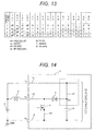
- FIG. 14 shows a conventional magnet coil drive control device that does not include the impedance element 7.
- the difference from this embodiment is the portion in a rectangle drawn with a dashed line.
- the conventional magnet coil drive control device has a circuit configuration in which the connecting point between the freewheeling diode 5 and the capacitor 6 is connected directly to the positive electrode line L1 on the power supply side via the connecting line L3. Therefore, to reduce ripple voltage, the capacitance of the capacitor 6 needs to be increased. As a result, the magnet coil drive control device 1 becomes larger in size by the amount equivalent to the increase in the capacitance of the capacitor 6.
- ripple voltage can be reduced by the impedance element 7. Accordingly, conduction noise can be efficiently suppressed, and the capacitance of the capacitor 6 can be made smaller.
- the magnet coil drive control device 1 can be made smaller in size.
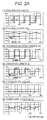
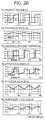
- FIGS. 2A and 2B show example cases where the voltage of the DC power supply 2 (an in-vehicle battery in this embodiment) is 14 V, the inductance of the coil of the solenoid 3 is 15 mH, the resistance value of the coil is 8 ⁇ , the drive frequency of the switching element 4 is 10 kHz, and the duty is 50%.
- the voltage of the DC power supply 2 an in-vehicle battery in this embodiment
- the inductance of the coil of the solenoid 3 is 15 mH
- the resistance value of the coil is 8 ⁇
- the drive frequency of the switching element 4 is 10 kHz
- the duty 50%.
- FIG. 2A shows a case where the capacitance of the capacitor 6 is 220 ⁇ F in the conventional magnet coil drive control device shown in FIG. 14 .
- FIG. 2B shows an example case where the capacitance of the capacitor 6 is 10 ⁇ F, and the impedance element 7 has a resistance value of 6 ⁇ in the magnet coil drive control device shown in FIG. 1 .
- the capacitance of the capacitor 6 is 1/22. In the description below, the behavior of the currents and the voltages of the respective circuit elements will be explained.
- the voltage of the solenoid 3 is the voltage on the drain side of the switching element 4. This is the on- or off-state in a case where the drive frequency is 10 kHz, and the duty is 50%.
- the drain voltage is approximately 0 V, and current flows into the solenoid 3.
- the drain voltage is approximately 14 V, and current is blocked from flowing into the solenoid 3.
- Solenoid current is the current on the drain side of the switching element 4.
- the DC power supply 2 and the solenoid 3 form a closed circuit, and the driving current flows into the solenoid 3.
- This driving current increases with time, and electrical energy is accumulated in the inductance of the solenoid 3.
- the solenoid 3, the freewheeling diode 5, and the impedance element 7 form a closed circuit, and a freewheeling current flows.
- the freewheeling current flows so that the electrical energy accumulated in the inductance of the solenoid 3 is released, and the current decreases with time.
- the impedance element 7 is not provided, and therefore, the charge in the capacitor 6 is not consumed as will be described later.
- a freewheeling current is the current that flows when the switching element 4 is in an off-state, and the solenoid 3, the freewheeling diode 5, and the impedance element 7 form a closed circuit.
- the current on the cathode side of the freewheeling diode 5 is shown.
- the anode voltage of the freewheeling diode 5 is 0 V, and therefore, the cathode voltage is high. That is, a reverse bias state is formed, and current does not flow.
- the impedance element 7 is not provided, and therefore, the charge in the capacitor 6 is not consumed, either, as will be described later.
- the DC power supply 2, the solenoid 3, the freewheeling diode 5, and the capacitor 6 form a closed circuit, and charge is accumulated in the capacitor 6.
- the switching element 4 is in an on-state, current does not flow into the freewheeling diode 5. Therefore, the charge accumulated so far flows out toward the impedance element 7.
- the current between the capacitor 6 and the connecting point (indicated as VC) between the connecting line L2 and the connecting line L3 is shown.
- the impedance element 7 is not provided, and therefore, the charge in the capacitor 6 flows out toward the positive electrode line L1.
- the voltage of the capacitor 6 (VC point) is 14 V, which is the voltage of the DC power supply 2, and is superimposed by the amount equivalent to the change in voltage caused by the capacitor current.
- Q represents the charge
- C represents the capacitance
- V represents the voltage between electrodes
- I the current flowing between electrodes
- T represents the time.
- the capacitor current is approximately 0.4 A
- the time is approximately 50 ⁇ s
- the capacitor current is approximately 0.4 A
- the time is approximately 50 ⁇ s
- the power-supply voltage is the voltage of the positive electrode line L1 or the terminal T1.
- the amount of the ripple voltage of the power supply is determined from the difference between the maximum voltage and the minimum voltage, and is as low as several hundreds of mV in this example. This is because the capacitance of the capacitor 6 is as high as 220 ⁇ F, and therefore, the change in voltage is small, though the charge in the capacitor 6 propagates directly to the positive electrode line L1 in the circuit configuration. However, if the capacitor 6 is made larger in this manner, the magnet coil drive control device becomes larger in size, which is not preferable.
- the ripple voltage of the power supply is also as low as several hundreds of mV. This is because, even if the capacitance of the capacitor 6 is greatly reduced, the voltage (approximately 2.5 V in this case) generated in the capacitor 6 is consumed by the impedance element 7 and does not appear on the positive electrode line L1, since the impedance element 7 is provided between the capacitor 6 and the positive electrode line L1. In this manner, the capacitance of the capacitor 6 can be reduced while conduction noise is suppressed. Accordingly, the magnet coil drive control device can be made smaller in size.
- the voltage of the terminal T1 is fixed at 14 V, and the ripple voltage of the power supply is 0 V.
- the voltage of the terminal T1 is fixed at 14 V, and the ripple voltage of the power supply is 0 V.
- the voltage corresponding to the partial pressure ratio between the wiring impedance and the impedance element 7 is observed.
- the wiring inductance is 10 ⁇ H, for example, the wiring impedance (reactance) is approximately 0.6 ⁇ .
- the conventional magnet coil drive control device is designed to suppress conduction noise with the high-capacitance capacitor 6, and accordingly, can suppress conduction noise.
- the capacitance thereof is high, and the magnet coil drive control device becomes larger in size.
- the magnet coil drive control device can be made smaller in size.
- the international standards include CISPR25 (1995) "Limits and methods of measurement of radio disturbance characteristics for the protection of receivers used on board vehicles", which is a standard created by International Special Committee on Radio Interference (CISPR).
- the CISPR25 standard relates to radio interference in the frequency band of 150 kHz to 1,000 MHz, and is applied to electronic components to be used in vehicles.
- the recommended values are set for protecting receivers in a vehicle from interfering waves generated from components and modules in the same vehicle, and the receivers to be protected are radio receivers, television receivers, and radio devices, for example.
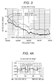
- the noise spectra of the embodiment shown in FIG. 1 and the conventional example shown in FIG. 14 were measured in accordance with this standard.
- the noise spectra are noise derived from the voltage of the power-supply line between the terminal T1 and the DC power supply 2.
- the frequency ranges from 100 kHz to 500 kHz.
- the capacitance of the capacitor 6 is set at 220 ⁇ F.
- the capacitance of the capacitor 6 is set at 10 ⁇ F
- the impedance element 7 is a resistor
- the resistance value of the resistor is set at 6 ⁇ .
- the noise level at a measurement frequency of 100 kHz was 69 dB ⁇ V in the conventional example (indicated by the dashed line), and was 64 dB ⁇ V in this embodiment (indicated by the solid line) . Further, it is clear that the noise level becomes lower as the measurement frequency becomes higher, but the noise level is kept lower in this embodiment than in the conventional example.
- the noise suppressing effect is increased according to this embodiment as indicated by the solid line, compared with the noise suppressing effect (noise level) achieved by the conventional example as indicated by the dashed line. Accordingly, the noise level in this embodiment is lower than that in the conventional example.
- FIG. 4A shows the amount of the ripple voltage in the conventional example shown in FIG. 14
- FIG. 4B shows the amount of the ripple voltage in this embodiment shown in FIG. 1 .
- the ripple voltage is 0.4 V in the conventional example
- the ripples voltage is reduced to 0.2 V according to this embodiment. As can be seen from that, the amount of the ripple voltage is almost halved, and the noise level is efficiently lowered.
- FIG. 5 shows the relationship between the driving current flowing in the solenoid 3 and the ripple voltage, with respect to the resistance value of the impedance element 7.
- the amplitude of the ripple voltage can be made smaller as the resistance value of the impedance element 7 becomes higher.
- this ripple voltage is observed as the voltage corresponding to the partial pressure ratio between the wiring impedance from the DC power supply 2 and the impedance element 7. Accordingly, as the value of the impedance element 7 becomes higher, the partial pressure ratio becomes higher, and the ripple voltage becomes lower.
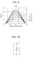
- FIG. 6 shows the relationship between the driving current in the solenoid 3 and loss in the impedance element 7, with respect to the resistance value of the impedance element 7.
- the loss becomes larger as the resistance value of the impedance element 7 becomes higher.
- the loss is caused by the impedance element 7 and the current flowing in the impedance element 7. Therefore, if the solenoid current stays the same, the loss is proportional to the resistance value of the impedance element 7.
- the ripple voltage and the loss in the impedance element 7 are in an inverse relationship That is, to reduce conduction noise, the resistance value of the impedance element 7 is preferably increased. In view of loss, however, the resistance of the impedance element 7 is preferably lowered. Accordingly, the range of the value of the impedance element 7 is spontaneously defined based on the range in which the ripple voltage is allowed, and the range in which the loss in the impedance element 7 is allowed. For example, a resistance value of 6 ⁇ is selected in a case where the maximum value of the ripple voltage is 0.4 V or lower, and the loss in the impedance element is allowed up to 0.7W. A resistance value of 2 ⁇ is selected in a case where the maximum value of the ripple voltage is 1.4 V or lower, and the loss in the impedance element is allowed up to 0.4 W.
- the resistance value of the impedance element 7 can be appropriately selected in accordance with the specifications of the magnet coil drive control device based on the relationship between the ripple voltage and the loss. In short, a resistance value that can efficiently reduce conduction noise and loss should be selected.
- the impedance element 7 is a resistor.
- the impedance element 7 may be a combination of a resistor and a passive element that is not a resistor, an active element, or another resistor, as shown in FIGS. 7A through 7F .
- FIGS. 7A through 7F specific structures of such impedance elements 7 are described.
- a resistor is the fundamental component so as to efficiently reduce noise, and this resistor is combined with one or more other impedance elements.
- FIG. 7A shows an example where one resistor is used as the impedance element 7. As only one resistor is used, the installation area of the circuit can be reduced, and costs can also be effectively lowered.
- FIG. 7B shows an example where two resistors arranged in parallel are used as the impedance element 7.
- the loss in the impedance element 7 is proportional to the square of the current flowing therein. Therefore, it is divided between a resistor Ra and a resistor Rb, so that the loss in each of the resistors is effectively halved.
- FIG. 7C shows an example where the impedance element 7 is formed with resistors (two resistors in this example) and resistance adjusting elements or switching elements for selecting the respective resistors.
- resistors two resistors in this example
- a resistor Rx and a resistor Ry preferably have different resistance values .
- different selections can be made depending on a combination of switching on and switching off of a switch SWx and a switch SWy. For example, if one resistance value is set at a large value while the other resistance value is set at a small value, conduction noise is more strongly suppressed when the one resistance value is selected, and loss can be made even smaller when the other resistance value is selected.
- FIG. 7D shows an example where the impedance element 7 is formed with a structure in which a resistor is connected in parallel between the collector and the emitter of a bipolar transistor TR having the function of a resistance adjusting element.
- the base current of the bipolar transistor TR is controlled, the on-state resistance between the collector and the emitter is changed, and a resistance in parallel with a resistor R can be formed. Accordingly, the resistance value can be changed in a non-step manner. This has the effect to suppress conduction noise and appropriately select loss. If the bipolar transistor TR breaks down in an off-state, the resistor R can be used singly. Thus, a fail-safe function can be provided.
- FIG. 7E shows an example where the impedance element 7 is formed with a combination of a resistor R and an inductance L arranged in series. This structure is effective in increasing the frequency impedance in a high-frequency band, or in suppressing high-frequency conduction noise.
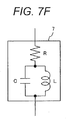
- FIG. 7F shows an example where a resistor R and a parallel resonance circuit formed with an inductance L and a capacitor C are connected in series to form the impedance element 7. This structure is effective in increasing the impedance at a certain frequency, or in suppressing certain conduction noise.
- the impedance element 7 shown in FIG. 7E or FIG. 7F it is very easy to appropriately combine a resistor with an inductance and a capacitor. Also, not having loss, an inductance and a capacitor are preferable as an impedance element.
- the impedance element 7 and the capacitor 6 are provided on the connecting line L3 connecting the positive electrode line L1 and the negative electrode line L5 of the DC power supply, and are arranged in series in the direction from the positive electrode line L1 toward the negative electrode line L5.
- the connecting line L3 between the impedance element 7 and the capacitor 6 is connected to one end of the solenoid 3 via the freewheeling diode so that a freewheeling current flows into the impedance element 7 and the capacitor 6.
- the portion between the anode side of the freewheeling diode 5 and the one end of the solenoid 3 is connected to the negative electrode line L3 by the low-side switching element 4.
- the magnet coil drive control device can be made smaller in size.
- two solenoids 3 are used, and the two solenoids 3 are magnet coils of hydraulic control valves that are used as an inlet valve and an outlet valve in a valve timing control device, for example.
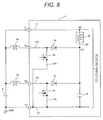
- the embodiment shown in FIG. 8 is characterized by including two drive circuits that are the same as the drive circuit shown in FIG. 1 , and having an impedance element 7 and a capacitor 6 shared between the two drive circuits.
- the functions of the impedance element 7 and the capacitor 6 are substantially the same as the functions of the impedance element 7 and the capacitor 6 shown in FIG. 1 . Therefore, explanation of the functions of the impedance element 7 and the capacitor 6 will not be made, and the circuit configurations will be described below.
- One of the drive circuits is formed with a solenoid 3a, a connecting line L2a, a switching element 4a, and a freewheeling diode 5a
- the other one of the drive circuits is formed with a solenoid 3n, a connecting line L2n, a switching element 4n, and a freewheeling diode 5n.
- the fundamental connections among them are substantially the same as those in the circuit shown in FIG. 1 .
- the respective cathodes of the freewheeling diode 5a and the freewheeling diode 5n are connected to a connecting line L3 between the impedance element 7 and the capacitor 6.
- the capacitance of the capacitor 6 and the resistance value of the impedance element 7 need to be adjusted to a value suitable for the two drive circuits.
- the embodiment shown in FIG. 9 is a modification of the embodiment shown in FIG. 8 .
- Two drive circuits that are the same as the drive circuit shown in FIG. 1 are provided, and impedance elements and capacitors are provided in the respective drive circuits.
- the functions of the impedance elements 7 and the capacitors 6 are also substantially the same as the functions of the impedance element 7 and the capacitor 6 shown in FIG. 1 . Therefore, explanation of the functions of the impedance elements 7 and the capacitors 6 will not be made, and the circuit configurations will be described below.
- One of the drive circuits is formed with a solenoid 3a, a connecting line L2a, a switching element 4a, and a freewheeling diode 5a
- the other one of the drive circuits is formed with a solenoid 3n, a connecting line L2n, a switching element 4n, and a freewheeling diode 5n.
- the cathode of the freewheeling diode 5a as well as an impedance element 7a and a capacitor 6a are connected to a line L3a
- the cathode of the freewheeling diode 5n as well as an impedance element 7n and a capacitor 6n are connected to a line L3n.
- the fundamental connections among them are substantially the same as those in the circuit shown in FIG. 1 .
- the impedance elements 7a and 7n, and the capacitors 6a and 6n exist in the two drive circuits independently of each other. This is particularly effective in reducing loss in the impedance elements 7.
- the impedance element 7 is shared between the two drive circuits, and therefore, the resistance value of the impedance element 7 becomes higher. As a result, loss might become large as shown in FIG. 6 .
- the impedance elements 7a and 7n are provided in the respective drive circuits. Accordingly, the resistance value can be made lower, and loss can be made smaller.
- each impedance element 7 is a resistor in this embodiment, it is possible to use any of the impedance elements 7 having the structures shown in FIGS. 7A through 7F .
- capacitor (s) 6 and impedance element (s) 7 can be provided in drive circuits with solenoids 3. Accordingly, conduction noise is reduced, and the capacitance of the capacitor(s) is reduced. Thus, the magnet coil drive control device can be made smaller in size.
- the switching element 4 is a low-side switch. In the third embodiment, however, the switching element 4 is a high-side switch.
- the functions of the impedance element 7 and the capacitor 6 are substantially the same as the functions of the impedance element 7 and the capacitor 6 shown in FIG. 1 . Therefore, explanation of the functions of the impedance element 7 and the capacitor 6 will not be made, and the circuit configurations will be described below.
- Terminals T1, T2, and T3 are provided in the magnet coil drive control device 1.
- the terminal T1 is connected to a DC power supply 2 such as the positive electrode terminal of an in-vehicle battery
- the terminal T2 is connected to the negative electrode terminal of the DC power supply 2
- the terminal T3 is connected to the positive electrode terminal of the DC power supply 2 via a solenoid 3.
- This solenoid 3 is a coil for forming an electromagnet, and the hydraulic control valve shifts in position depending on the current flowing in the solenoid 3. Accordingly, the oil quantity of the hydraulic mechanism can be adjusted.
- This type of mechanism is well known, and therefore, will not be described in detail herein.
- the terminal T1 is connected to a positive electrode line L1 in the magnet coil drive control device 1, and the terminal T2 is connected to a negative electrode line L5 in the magnet coil drive control device 1.
- the positive electrode line L1 and the negative electrode line L5 are connected by a connecting line L3, and, on the connecting line L3, a capacitor 6 and an impedance element 7 are arranged and connected in series in the direction from the positive electrode line L3 toward the negative electrode line L5.
- the connecting line L3 between the capacitor 6 and the impedance element 7 is connected to one end of the solenoid 3 by a connecting line L2, and a freewheeling diode 5 is provided on the connecting line L2.
- the anode side of the freewheeling diode 5 is connected to the connecting line L3 between the capacitor 6 and the impedance element 7, and the cathode side of the freewheeling diode 5 is connected to the one end of the solenoid 3.
- the portion between the cathode side of the freewheeling diode 5 and the one end of the solenoid 3 is connected to the positive electrode line L1 by a connecting line L4, and a switching element 4 as a high-side switch is connected to the connecting line L4.
- This switching element 4 is a MOS-FET, the source side of the switching element 4 is connected to the portion between the cathode side of the freewheeling diode 5 and the one end of the solenoid 3, and the drain side of the switching element 4 is connected to the positive electrode line L1.
- the positive electrode side of the DC power supply 2 is connected to another circuit in the magnet coil drive control device 1 via the positive electrode line L1, and the GND side of the DC power supply 2 is connected to another circuit in the magnet coil drive control device 1 via the negative electrode line L5, so that power is supplied thereto.
- this aspect is not relevant to the present invention, and will not be described in detail herein.
- the switching element 4 is a high-side switch. Therefore, the behavior of the freewheeling current differs from that of the first embodiment, but the principle thereof is the same.
- the switching element 4 transits to an on-state, the drain voltage becomes 0 V, and current flows into the solenoid 3.
- the current flowing into the solenoid 3 is the driving current that flows into the solenoid 3 as the DC power supply 2 and the solenoid 3 form a closed circuit when the switching element 4 is in an on-state. This driving current increases with time, and electrical energy is accumulated in the inductance of the solenoid 3.
- the solenoid 3 When the switching element 4 transits to an off-state, on the other hand, the solenoid 3, the freewheeling diode 5, and the impedance element 7 form a closed circuit, and a freewheeling current flows.
- the freewheeling current flows so that the energy accumulated in the inductance of the solenoid 3 is released, and the current decreases with time.
- the freewheeling current is the current that flows as the solenoid 3, the freewheeling diode 5, and the impedance element 7 form a closed circuit when the switching element 4 is in an off-state.
- the cathode voltage of the freewheeling diode 5 is 14 V, and therefore, the cathode voltage is high. That is, a reverse bias state is formed, and any freewheeling current does not flow.
- the switching element 4 when the switching element 4 is in an off-state, the DC power supply 2, the solenoid 3, the freewheeling diode 5, and the capacitor 6 form a closed circuit, and charge is accumulated in the capacitor 6.
- the switching element 4 when the switching element 4 is in an on-state, on the other hand, current does not flow into the freewheeling diode 5. Therefore, the charge accumulated in the capacitor 6 while the switching element 4 is in an off-state flows out toward the impedance element 7.
- the charge (voltage) accumulated in the capacitor 6 is applied to the negative electrode line L5.
- the impedance element 7 provided between the capacitor 6 and the negative electrode line L5 in this embodiment. Therefore, the charge accumulated in the capacitor 6 is consumed by the impedance element 7, and does not appear on the negative electrode line L5. With this, ripple voltage generation is restrained on the negative electrode line L5, and conduction noise can be reduced. This ripple voltage is conduction noise at the high frequency corresponding to the on/off ratio in the solenoid 3.
- the capacitor 6 and the impedance element 7 are provided on the connecting line L3 connecting the positive electrode line L1 and the negative electrode line L5 of the DC power supply, and are arranged in series in the direction from the positive electrode line L1 toward the negative electrode line L5.
- the connecting line L3 between the capacitor 6 and the impedance element 7 is connected to one end of the solenoid 3 via the freewheeling diode so that a freewheeling current flows toward the solenoid side.
- the portion between the cathode side of the freewheeling diode 5 and the one end of the solenoid 3 is connected to the positive electrode line L1 by the high-side switching element 4.
- the magnet coil drive control device can be made smaller in size.
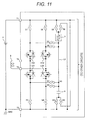
- This embodiment shows a motor drive control device that uses an H-bridge circuit.
- the functions of the impedance element 7 and the capacitor 6 are substantially the same as the functions of the impedance element 7 and the capacitor 6 shown in FIG. 1 . Therefore, explanation of the functions of the impedance element 7 and the capacitor 6 will not be made, and the circuit configurations will be described below.
- the configuration of the drive circuit of the magnet coil drive control device is described.
- This embodiment is characterized by switching between the impedance element 7 and the capacitor 6 used in an H-bridge circuit. That is, the H-bridge circuit is a preferred circuit configuration for controlling a motor, and is characterized by controlling the connection state between the impedance element 7 and the capacitor 6 in accordance with the operating states of four MOS-FETs.
- MOS-FETs are used in the H-bridge circuit, and high-side switching elements HS1 and HS2, and low-side switching elements LS1 and LS2 are connected to terminals T5 and T6 of a magnet coil 3 of a motor.
- the relationship of connection among the terminals T5 and T6 of the magnet coil 3, the high-side switching elements HS1 and HS2, and the low-side switching elements LS1 and LS2 is a well-known relationship.
- Each MOS-FET has a parasitic diode formed between the source and the drain, or includes a so-called body diode.
- the drain side of the high-side switching element HS1 and the drain side of the high-side switching element HS2 are connected to the power supply side of a DC power supply 2 via a terminal T1 through a switch S1 and a switch S2, respectively.
- the source side of the low-side switching element LS1 and the source side of the low-side switching element LS2 are connected to the GND side of the DC power supply 2 via a terminal T2 through a switch S3 and a switch S4, respectively.
- the source side of the high-side switching element HS1, the drain side of the low-side switching element LS1, and one end of the magnet coil 3 are connected by the terminal T5
- the source side of the high-side switching element HS2, the drain side of the low-side switching element LS2, and the other end of the magnet coil are connected by the terminal T6.
- This circuit forms an H-bridge circuit that drives a motor.
- the impedance element 7 and the capacitor 6 have the circuit configurations described below.
- the impedance element 7 and the capacitor 6 are connected to the power supply side of the DC power supply 2 through a switch S9 and a switch SC, respectively.
- the impedance element 7 and the capacitor 6 are further connected to the GND side of the DC power supply 2 through a switch SB and a switch SA, respectively.
- a connecting line L3 between the impedance element 7 and the capacitor 6 is connected to the drain side of the high-side switching element HS1 through a switch S5, and is connected to the drain side of the high-side switching element HS2 through a switch S6.
- the connecting line L3 is connected to the source side of the low-side switching element LS1 through a switch S7, and is connected to the source side of the low-side switching element LS2 through a switch S8.
- FIG. 13 shows the on- or off-states of the switching elements HS1, HS2, LS1, and LS2, and the on- or off-states of the switches S1 through SC in the respective operating states.
- the on- or off-states of the switching elements HS1, HS2, LS1, and LS2, and the on- or off-states of the switches S1 through SC are controlled by an electronic control unit not shown in the drawing.
- the high-side switching element HS2 enters an on-state, and the low-side switching element LS1 serves as the low-side switch and is repeatedly switched on and off by a control signal from the electronic control unit.
- the high-side switching element HS1 enters an on-state, and the low-side switching element LS2 serves as the low-side switch and is repeatedly switched on and off by a control signal from the electronic control unit.
- the operation mode 1 and the operation mode 2 are the same as the embodiment using the low-side switching element 4 shown in FIG. 1 .
- the low-side switching element LS2 enters an on-state, and the high-side switching element HS1 serves as the high-side switch and is repeatedly switched on and off by a control signal from the electronic control unit.
- the low-side switching element L1 enters an on-state, and the high-side switching element HS2 serves as the high-side switch and is repeatedly switched on and off by a control signal from the electronic control unit.
- the operation mode 3 and the operation mode 4 are the same as the embodiment using the high-side switching element 4 shown in FIG. 10 .
- the respective switches S1 through SC are selected and driven in accordance with operations of the respective switching elements HS1, HS2, LS1, and LS2.
- the settings in the H-bridge circuit are as shown in FIG. 13 . That is, the switch S2 and the switch S3 are put into an on-state, and the switch S1 and the switch S4 are put into an off-state.
- the high-side switching element HS2 is put into an on-state, and the high-side switching element HS1 and the low-side switching element LS2 are put into an off-state.
- the body diode included in the high-side switching element HS1 is equivalent to a freewheeling diode.
- the low-side switching element LS1 is put into an switching state and is repeatedly switched on and off in accordance with a control signal (an on/off signal) applied from the electronic control unit.
- the switch S9 is put into an on-state, and the switch SB is put into an off-state. With this, the impedance element 7 is connected to the power supply side of the DC power supply 2.
- the switch SA is put into an on-state, and the switch SC is put into an off-state. With this, the capacitor 6 is connected to the GND side of the DC power supply 2.
- the setting state of the operation mode 1 set in the above described manner is set to the same low-side switch as that in the circuit configuration of the first embodiment. Operation of this circuit is the same as that of the first embodiment, and therefore, will not be described in detail.
- the H-bridge circuit is formed with a combination of two half-bridge circuits arranged on the right and left sides.
- Each of the half-bridge circuits has the characteristics of both a low-side switch and a high-side switch. Accordingly, if switches in the H-bridge circuit are appropriately selected, the impedance element and the capacitor of the first embodiment or the third embodiment can be used in conjunction with the H-bridge circuit.
- a capacitor and an impedance element are arranged in series on the connecting line connecting the positive electrode line and the negative electrode line of a DC power supply, the connecting line between the capacitor and the impedance element is connected to one end of a magnet coil via a freewheeling diode, and the portion between the freewheeling diode and the one end of the magnet coil is connected to the positive electrode line or the negative electrode line by a switching element.
- the magnet coil drive control device can be made smaller in size.
Landscapes
- Engineering & Computer Science (AREA)
- Physics & Mathematics (AREA)
- Electromagnetism (AREA)
- Power Engineering (AREA)
- Chemical & Material Sciences (AREA)
- Combustion & Propulsion (AREA)
- Mechanical Engineering (AREA)
- General Engineering & Computer Science (AREA)
- Electronic Switches (AREA)
Abstract
Description
- The present invention relates to a magnet coil drive control device to be used in an adjustment mechanism that uses an electromagnet or in a motor, and more particularly, to a magnet coil drive control device to which electrical power is supplied from a DC power supply.
- For automobiles and the like, there is a demand for improvements of the fuel efficiency (fuel consumption) of internal-combustion engines, not only to cope with environmental issues and comply with exhaust emission regulations, but also to meet the increase in awareness of energy conversion and prevent resource depletion. Therefore, the combustion efficiency of internal-combustion engines is increased to reduce the fuel used in combustion, and further, the hazardous components in emissions are reduced.
- As an example for increasing the combustion efficiency of an internal-combustion engine, a valve timing control (VTC) device is known. The valve timing control device optimizes the timings to open and close the inlet valve and the outlet valve based on the engine speed and the intake air quantity (load) of the internal-combustion engine. This valve timing control device includes a hydraulic mechanism that rotates a cam shaft in a relative manner, and controls the position of a hydraulic control valve that uses an electromagnet. In this manner, the oil quantity of the hydraulic mechanism is adjusted so that the timings to open and close the inlet valve and the outlet valve are changed.
- Other than the valve timing control device, a gearshift control valve that is used in an automatic transmission, an electronic throttle control device provided in an air intake passage, or the like is used to improve fuel efficiency. Such devices have electromagnets and motors as principal drive sources, and are driven and controlled by electrical power supplied to magnet coils. In view of the above, a magnet coil drive control device that controls power to be supplied to an electromagnet or the magnet coil of a motor is essential in operating the mechanical part of an automobile.
- For example, in a drive control device for driving a magnet coil according to
JP 2006-35190 A PTL 1 discloses a method of shortening the time of attenuation of inductive current generated in the magnet coil, so as to restrain increases in the temperature of the magnet coil. - PTL 1:
JP 2006-351910 A - In a magnet coil drive control device that drives and controls a magnet coil, when the current flowing into the magnet coil is turned on and off to drive the magnet coil in an excited state or an unexcited state, conduction noise is generated in a cable connected to the positive electrode of the DC power supply or a wire of a substrate pattern or the like, due to the turning on and off of the current flowing into the magnet coil.
- In conventional cases, a method of absorbing conduction noise by providing a high-capacitance capacitor on a wire has been popular. In recent year, however, there has been an increasing demand for decreases in size of high-capacitance capacitors and effective restraints on conduction noise, for reasons such as the decrease in size of each magnet coil drive control device.
- To respond to such a demand, the present invention aims to provide a magnet coil drive control device that can efficiently suppress conduction noise while reducing the capacitance of a capacitor.
- The present invention is characterized in that a capacitor and an impedance element are arranged in series on the connecting line connecting the positive electrode line and the negative electrode line of a DC power supply, the connecting line between the capacitor and the impedance element is connected to the opposite end of a magnet coil connected to the positive electrode side of the DC power supply via a freewheeling diode, and the connecting line between the freewheeling diode and the end of the magnet coil is connected to the positive electrode line or the negative electrode line by a connecting line having a switching element thereon. Here, the switching element serves as the high-side switch when connected to the positive electrode line, and serves as the low-side switch when connected to the negative electrode line.
- According to the present invention, conduction noise caused by the driving current of a magnet coil can be suppressed by an impedance element, and the capacitance of a capacitor can be further reduced. Accordingly, a magnet coil drive control device can be made smaller in size.
-
- [
FIG. 1] FIG. 1 is a circuit diagram showing the circuit configuration of a magnet coil drive control device according to a first embodiment of the present invention. - [
FIG. 2A] FIG. 2A is an explanatory diagram showing changes in the voltage and the current of a magnet coil, the current of a freewheeling diode, the voltage and the current of a capacitor, and a power-supply voltage, to explain conduction noise in a conventional magnet coil drive control device. - [
FIG. 2B] FIG. 2B is an explanatory diagram showing changes in the voltage and the current of a magnet coil, the current of a freewheeling diode, the voltage and the current of a capacitor, and a power-supply voltage, to explain conduction noise in the magnet coil drive control device shown inFIG. 1 . - [
FIG. 3] FIG. 3 is an explanatory diagram showing noise spectra for comparing the magnet coil drive control device shown inFIG. 1 with the conventional magnet coil drive control device. - [
FIG. 4A] FIG. 4A is a characteristic diagram showing the ripple voltage of the power supply for the conventional magnet coil drive control device. - [
FIG. 4B] FIG. 4B is a characteristic diagram showing the ripple voltage of the power supply for the magnet coil drive control device shown inFIG. 1 . - [
FIG. 5] FIG. 5 is an explanatory diagram showing the relationship between the current flowing in a solenoid and the ripple voltage, with respect to the resistance value of an impedance element. - [
FIG. 6] FIG. 6 is an explanatory diagram showing the relationship between the current flowing in a solenoid and loss, with respect to the resistance value of an impedance element. - [
FIG. 7A] FIG. 7A is an explanatory diagram of a circuit element, showing a first example of an impedance element. - [
FIG. 7B] FIG. 7B is an explanatory diagram of a circuit element, showing a second example of an impedance element. - [
FIG. 7C] FIG. 7C is an explanatory diagram of a circuit element, showing a third example of an impedance element. - [
FIG. 7D] FIG. 7D is an explanatory diagram of a circuit element, showing a fourth example of an impedance element. - [
FIG. 7E] FIG. 7E is an explanatory diagram of a circuit element, showing a fifth example of an impedance element. - [
FIG. 7F] FIG. 7F is an explanatory diagram of a circuit element, showing a sixth example of an impedance element. - [
FIG. 8] FIG. 8 is a circuit diagram showing the circuit configuration of a magnet coil drive control device according to a second embodiment of the present invention. - [
FIG. 9] FIG. 9 is a circuit diagram showing the circuit configuration of a magnet coil drive control device according to a modification of the second embodiment shown inFIG. 8 . - [
FIG. 10] FIG. 10 is a circuit diagram showing the circuit configuration of a magnet coil drive control device according to a third embodiment of the present invention. - [
FIG. 11] FIG. 11 is a circuit diagram showing the circuit configuration of a magnet coil drive control device according to a fourth embodiment of the present invention. - [
FIG. 12] FIG. 12 is a circuit diagram for explaining operating states of the magnet coil drive control device according to the fourth embodiment shown inFIG. 11 . - [
FIG. 13] FIG. 13 is an explanatory diagram for explaining operating states of the respective switching elements of the magnet coil drive control device according to the fourth embodiment shown inFIG. 11 . - [
FIG. 14] FIG. 14 is a circuit diagram showing the circuit configuration of the conventional magnet coil drive control device. - The following is a detailed description of embodiments of the present invention, with reference to the accompanying drawings. However, the present invention is not limited to the embodiments described below, and various modifications and applications fall within the technical scope of the invention.
- Referring now to
FIG. 1 , a first embodiment of the present invention is described in detail. InFIG. 1 ,reference numeral 1 indicates a magnet coil drive control device according to the present invention, and a circuit element that controls the current flowing into amagnet coil 3 is provided therein. Themagnet coil 3 is used in various kinds of adjusting mechanisms, and, in this embodiment, is a magnet coil of a hydraulic control valve that is used in a valve timing control device. A hydraulic control valve is a control valve that linearly shifts in position depending on the magnitude of electrical current, and can control the position of a needle in accordance with the average current value that varies with the on/off ratio (duty) of the driving current. A direct-driven electrical device of this type is normally called a solenoid, and therefore, themagnet coil 3 will be hereinafter referred to as thesolenoid 3. This drawing shows the circuit element that drives thesolenoid 3, and explanation of circuit elements other than that will not be made below. - Terminals T1, T2, and T3 are provided in the magnet coil
drive control device 1. The terminal T1 is connected to aDC power supply 2 such as the positive electrode terminal of an in-vehicle battery, the terminal T2 is connected to the negative electrode terminal of theDC power supply 2, and the terminal T3 is connected to the positive electrode terminal of theDC power supply 2 via thesolenoid 3. Thissolenoid 3 is a coil for forming an electromagnet, and the hydraulic control valve shifts in position depending on the current flowing in thesolenoid 3. Accordingly, the oil quantity of the hydraulic mechanism can be adjusted. This type of mechanism is well known, and therefore, will not be described in detail herein. - The terminal T1 is connected to a positive electrode line L1 in the magnet coil
drive control device 1, and the terminal T2 is connected to a negative electrode line L5 in the magnet coildrive control device 1. The positive electrode line L1 and the negative electrode line L5 are connected by a connecting line L3, and, on the connecting line L3, animpedance element 7 and acapacitor 6 are arranged and connected in series in the direction from the positive electrode line L1 toward the negative electrode line L5. The connecting line L3 between thecapacitor 6 and theimpedance element 7 is connected to one end of thesolenoid 3 by a connecting line L2, and afreewheeling diode 5 is provided on the connecting line L2. The cathode side of thefreewheeling diode 5 is connected to the connecting line L3 between thecapacitor 6 and theimpedance element 7, and the anode side of thefreewheeling diode 5 is connected to the one end of thesolenoid 3. - Here, various kinds of capacitors including an electrolytic capacitor can be used as the
capacitor 6. In this embodiment, however, a ceramic capacitor is used, because a ceramic capacitor is suitable for restraining noise generation, having a low equivalent series resistance (ESR). - Further, the portion between the anode side of the
freewheeling diode 5 and the one end of thesolenoid 3 is connected to the negative electrode line L5 by a connecting line L4, and aswitching element 4 as a low-side switch is connected to the connecting line L4. This switchingelement 4 is a MOS-FET, the drain side of theswitching element 4 is connected to the portion between the anode side of thefreewheeling diode 5 and the one end of thesolenoid 3, and the source side of theswitching element 4 is connected to the negative electrode line L5. - The positive electrode side of the
DC power supply 2 is connected to another circuit in the magnet coildrive control device 1 via the positive electrode line L1, and the GND side of theDC power supply 2 is connected to another circuit in the magnet coildrive control device 1 via the negative electrode line L5, so that power is supplied thereto. However, this aspect is not relevant to the present invention, and will not be described in detail herein. - In the above described structure, when a predetermined control signal is supplied to the gate of the
switching element 4, the switchingelement 4 transits to an on-state, the drain voltage becomes 0 V, and current flows into thesolenoid 3. The current flowing into thesolenoid 3 is the driving current flowing into thesolenoid 3 as theDC power supply 2 and thesolenoid 3 form a closed circuit when the switchingelement 4 is in an on-state. This driving current increases with time, and electrical energy is accumulated in the inductance of thesolenoid 3. - When the switching
element 4 transits to an off-state, on the other hand, thesolenoid 3, the freewheelingdiode 5, and theimpedance element 7 form a closed circuit, and a freewheeling current flows. The freewheeling current flows so that the electrical energy accumulated in the inductance of thesolenoid 3 is released, and the current decreases with time. The freewheeling current is the current that flows as thesolenoid 3, the freewheelingdiode 5, and theimpedance element 7 form a closed circuit when the switchingelement 4 is in an off-state. When the switchingelement 4 is in an on-state, the voltage on the anode side of thefreewheeling diode 5 is 0 V, and therefore, the cathode voltage is high. That is, a reverse bias state is formed, and current does not flow. - Furthermore, when the switching
element 4 is in an off-state, theDC power supply 2, thesolenoid 3, the freewheelingdiode 5, and thecapacitor 6 form a closed circuit, and charge is accumulated in thecapacitor 6. When the switchingelement 4 is in an on-state, on the other hand, current does not flow into thefreewheeling diode 5. Therefore, the charge accumulated in thecapacitor 6 while theswitching element 4 is in an off-state flows out toward theimpedance element 7. The charge accumulated in thecapacitor 6 is applied to the positive electrode line L1. However, there is theimpedance element 7 provided between thecapacitor 6 and the positive electrode line L1 in this embodiment. Therefore, the charge accumulated in thecapacitor 6 is consumed by theimpedance element 7, and is not superimposed on the positive electrode line L1. With this, ripple voltage generation is restrained on the positive electrode line L1, and conduction noise can be reduced. This ripple voltage is conduction noise at the high frequency corresponding to the on/off ratio in thesolenoid 3. - For purpose of comparison with this embodiment,
FIG. 14 shows a conventional magnet coil drive control device that does not include theimpedance element 7. As can be seen fromFIG. 14 , the difference from this embodiment is the portion in a rectangle drawn with a dashed line. As shown inFIG. 14 , the conventional magnet coil drive control device has a circuit configuration in which the connecting point between thefreewheeling diode 5 and thecapacitor 6 is connected directly to the positive electrode line L1 on the power supply side via the connecting line L3. Therefore, to reduce ripple voltage, the capacitance of thecapacitor 6 needs to be increased. As a result, the magnet coildrive control device 1 becomes larger in size by the amount equivalent to the increase in the capacitance of thecapacitor 6. - In this embodiment, on the other hand, ripple voltage can be reduced by the
impedance element 7. Accordingly, conduction noise can be efficiently suppressed, and the capacitance of thecapacitor 6 can be made smaller. Thus, the magnet coildrive control device 1 can be made smaller in size. - Next, operation of the magnet coil drive control device according to the first embodiment shown in
FIG. 1 is described while being compared with operation of the conventional magnet coil drive control device shown inFIG. 14 .FIGS. 2A and2B show example cases where the voltage of the DC power supply 2 (an in-vehicle battery in this embodiment) is 14 V, the inductance of the coil of thesolenoid 3 is 15 mH, the resistance value of the coil is 8 Ω, the drive frequency of theswitching element 4 is 10 kHz, and the duty is 50%. -
FIG. 2A shows a case where the capacitance of thecapacitor 6 is 220 µF in the conventional magnet coil drive control device shown inFIG. 14 .FIG. 2B shows an example case where the capacitance of thecapacitor 6 is 10 µF, and theimpedance element 7 has a resistance value of 6 Ω in the magnet coil drive control device shown inFIG. 1 . In this embodiment, the capacitance of thecapacitor 6 is 1/22. In the description below, the behavior of the currents and the voltages of the respective circuit elements will be explained. - The voltage of the
solenoid 3 is the voltage on the drain side of theswitching element 4. This is the on- or off-state in a case where the drive frequency is 10 kHz, and the duty is 50%. When the switchingelement 4 is in an on-state, the drain voltage is approximately 0 V, and current flows into thesolenoid 3. When the switchingelement 4 is in an off-state, the drain voltage is approximately 14 V, and current is blocked from flowing into thesolenoid 3. - Solenoid current is the current on the drain side of the
switching element 4. When the switchingelement 4 is in an on-state, theDC power supply 2 and thesolenoid 3 form a closed circuit, and the driving current flows into thesolenoid 3. This driving current increases with time, and electrical energy is accumulated in the inductance of thesolenoid 3. When the switchingelement 4 is in an off-state, thesolenoid 3, the freewheelingdiode 5, and theimpedance element 7 form a closed circuit, and a freewheeling current flows. The freewheeling current flows so that the electrical energy accumulated in the inductance of thesolenoid 3 is released, and the current decreases with time. In the conventional magnet coil drive control device, theimpedance element 7 is not provided, and therefore, the charge in thecapacitor 6 is not consumed as will be described later. - A freewheeling current is the current that flows when the switching
element 4 is in an off-state, and thesolenoid 3, the freewheelingdiode 5, and theimpedance element 7 form a closed circuit. In each of the drawings, the current on the cathode side of thefreewheeling diode 5 is shown. When the switchingelement 4 is in an on-state, the anode voltage of thefreewheeling diode 5 is 0 V, and therefore, the cathode voltage is high. That is, a reverse bias state is formed, and current does not flow. In the conventional magnet coil drive control device in this case, theimpedance element 7 is not provided, and therefore, the charge in thecapacitor 6 is not consumed, either, as will be described later. - When the switching
element 4 is in an off-state, theDC power supply 2, thesolenoid 3, the freewheelingdiode 5, and thecapacitor 6 form a closed circuit, and charge is accumulated in thecapacitor 6. When the switchingelement 4 is in an on-state, current does not flow into thefreewheeling diode 5. Therefore, the charge accumulated so far flows out toward theimpedance element 7. In each of the drawings, the current between thecapacitor 6 and the connecting point (indicated as VC) between the connecting line L2 and the connecting line L3 is shown. In the conventional magnet coil drive control device, theimpedance element 7 is not provided, and therefore, the charge in thecapacitor 6 flows out toward the positive electrode line L1. - In the steady state, the voltage of the capacitor 6 (VC point) is 14 V, which is the voltage of the
DC power supply 2, and is superimposed by the amount equivalent to the change in voltage caused by the capacitor current. In each of the drawings, it is the voltage at the connecting point (indicated as VC) between the connecting line L2 and the connecting line L3. This voltage is normally determined according to V = IT/C based on Q = IT and Q = CV, and it becomes apparent that this voltage is proportional to the current, and is inversely proportional to the capacitance. Here, Q represents the charge, C represents the capacitance, V represents the voltage between electrodes, I represents the current flowing between electrodes, and T represents the time. - In the conventional magnet coil drive control device shown in
FIG. 2A , the capacitor current is approximately 0.4 A, the time is approximately 50 µs, and the electrostatic capacitance is 220 µF. Accordingly, the capacitor voltage is expressed as
- In the magnet coil drive control device shown in
FIG. 2B , the capacitor current is approximately 0.4 A, the time is approximately 50 µs, and the electrostatic capacitance is 10 µF. Accordingly, the capacitor voltage is expressed as
- The power-supply voltage is the voltage of the positive electrode line L1 or the terminal T1. In the conventional magnet coil drive control device shown in
FIG. 2A , the amount of the ripple voltage of the power supply is determined from the difference between the maximum voltage and the minimum voltage, and is as low as several hundreds of mV in this example. This is because the capacitance of thecapacitor 6 is as high as 220 µF, and therefore, the change in voltage is small, though the charge in thecapacitor 6 propagates directly to the positive electrode line L1 in the circuit configuration. However, if thecapacitor 6 is made larger in this manner, the magnet coil drive control device becomes larger in size, which is not preferable. - In the magnet coil drive control device according to this embodiment shown in
FIG. 2B , the ripple voltage of the power supply is also as low as several hundreds of mV. This is because, even if the capacitance of thecapacitor 6 is greatly reduced, the voltage (approximately 2.5 V in this case) generated in thecapacitor 6 is consumed by theimpedance element 7 and does not appear on the positive electrode line L1, since theimpedance element 7 is provided between thecapacitor 6 and the positive electrode line L1. In this manner, the capacitance of thecapacitor 6 can be reduced while conduction noise is suppressed. Accordingly, the magnet coil drive control device can be made smaller in size. - In a case where the impedance of the wires and the like between the
DC power supply 2 and theimpedance element 7 is 0 Ω, for example, the voltage of the terminal T1 is fixed at 14 V, and the ripple voltage of the power supply is 0 V. In reality, however, there exist a wiring inductance and a wiring resistance between theDC power supply 2 and theimpedance element 7, and therefore, there is some impedance. At the terminal T1 in that case, the voltage corresponding to the partial pressure ratio between the wiring impedance and theimpedance element 7 is observed. If the wiring inductance is 10 µH, for example, the wiring impedance (reactance) is approximately 0.6Ω. In a case where the change in theimpedance element 7 is 6 Ω, and the change in the voltage of thecapacitor 6 is 2.5 V, the ripple voltage can be V = 2.5 × 0. 6/ (0. 6 + 6) = 0.2 V, which is sufficiently low. - As described above, the conventional magnet coil drive control device is designed to suppress conduction noise with the high-
capacitance capacitor 6, and accordingly, can suppress conduction noise. However, the capacitance thereof is high, and the magnet coil drive control device becomes larger in size. - In this embodiment, on the other hand, conduction noise is sufficiently suppressed with the
impedance element 7 and thecapacitor 6, and the capacitance of thecapacitor 6 can be further reduced by a considerable amount. Accordingly, the magnet coil drive control device can be made smaller in size. - Next, the standards for conduction noise are briefly described. The international standards include CISPR25 (1995) "Limits and methods of measurement of radio disturbance characteristics for the protection of receivers used on board vehicles", which is a standard created by International Special Committee on Radio Interference (CISPR). The CISPR25 standard relates to radio interference in the frequency band of 150 kHz to 1,000 MHz, and is applied to electronic components to be used in vehicles. The recommended values are set for protecting receivers in a vehicle from interfering waves generated from components and modules in the same vehicle, and the receivers to be protected are radio receivers, television receivers, and radio devices, for example.
- The noise spectra of the embodiment shown in
FIG. 1 and the conventional example shown inFIG. 14 were measured in accordance with this standard. The noise spectra are noise derived from the voltage of the power-supply line between the terminal T1 and theDC power supply 2. As shown inFIG. 3 , the frequency ranges from 100 kHz to 500 kHz. In the conventional example shown inFIG. 14 , the capacitance of thecapacitor 6 is set at 220 µF. In this embodiment shown inFIG. 1 , the capacitance of thecapacitor 6 is set at 10 µF, theimpedance element 7 is a resistor, and the resistance value of the resistor is set at 6Ω. The noise level at a measurement frequency of 100 kHz was 69 dBµV in the conventional example (indicated by the dashed line), and was 64 dBµV in this embodiment (indicated by the solid line) . Further, it is clear that the noise level becomes lower as the measurement frequency becomes higher, but the noise level is kept lower in this embodiment than in the conventional example. - As can be seen from the above, the noise suppressing effect is increased according to this embodiment as indicated by the solid line, compared with the noise suppressing effect (noise level) achieved by the conventional example as indicated by the dashed line. Accordingly, the noise level in this embodiment is lower than that in the conventional example.
- Further,
FIG. 4A shows the amount of the ripple voltage in the conventional example shown inFIG. 14 , andFIG. 4B shows the amount of the ripple voltage in this embodiment shown inFIG. 1 . While the ripple voltage is 0.4 V in the conventional example, the ripples voltage is reduced to 0.2 V according to this embodiment. As can be seen from that, the amount of the ripple voltage is almost halved, and the noise level is efficiently lowered. -
FIG. 5 shows the relationship between the driving current flowing in thesolenoid 3 and the ripple voltage, with respect to the resistance value of theimpedance element 7. According to this embodiment, the amplitude of the ripple voltage can be made smaller as the resistance value of theimpedance element 7 becomes higher. As mentioned earlier, this ripple voltage is observed as the voltage corresponding to the partial pressure ratio between the wiring impedance from theDC power supply 2 and theimpedance element 7. Accordingly, as the value of theimpedance element 7 becomes higher, the partial pressure ratio becomes higher, and the ripple voltage becomes lower. -
FIG. 6 shows the relationship between the driving current in thesolenoid 3 and loss in theimpedance element 7, with respect to the resistance value of theimpedance element 7. According to this embodiment, the loss becomes larger as the resistance value of theimpedance element 7 becomes higher. The loss is caused by theimpedance element 7 and the current flowing in theimpedance element 7. Therefore, if the solenoid current stays the same, the loss is proportional to the resistance value of theimpedance element 7. - In the above manner, the ripple voltage and the loss in the
impedance element 7 are in an inverse relationship That is, to reduce conduction noise, the resistance value of theimpedance element 7 is preferably increased. In view of loss, however, the resistance of theimpedance element 7 is preferably lowered. Accordingly, the range of the value of theimpedance element 7 is spontaneously defined based on the range in which the ripple voltage is allowed, and the range in which the loss in theimpedance element 7 is allowed. For example, a resistance value of 6Ω is selected in a case where the maximum value of the ripple voltage is 0.4 V or lower, and the loss in the impedance element is allowed up to 0.7W. A resistance value of 2 Ω is selected in a case where the maximum value of the ripple voltage is 1.4 V or lower, and the loss in the impedance element is allowed up to 0.4 W. - In this manner, the resistance value of the
impedance element 7 can be appropriately selected in accordance with the specifications of the magnet coil drive control device based on the relationship between the ripple voltage and the loss. In short, a resistance value that can efficiently reduce conduction noise and loss should be selected. - In the above described example, the
impedance element 7 is a resistor. However, theimpedance element 7 may be a combination of a resistor and a passive element that is not a resistor, an active element, or another resistor, as shown inFIGS. 7A through 7F . Referring now toFIGS. 7A through 7F , specific structures ofsuch impedance elements 7 are described. In the structures suggested inFIGS. 7A through 7F , a resistor is the fundamental component so as to efficiently reduce noise, and this resistor is combined with one or more other impedance elements. -
FIG. 7A shows an example where one resistor is used as theimpedance element 7. As only one resistor is used, the installation area of the circuit can be reduced, and costs can also be effectively lowered. -
FIG. 7B shows an example where two resistors arranged in parallel are used as theimpedance element 7. The loss in theimpedance element 7 is proportional to the square of the current flowing therein. Therefore, it is divided between a resistor Ra and a resistor Rb, so that the loss in each of the resistors is effectively halved. -
FIG. 7C shows an example where theimpedance element 7 is formed with resistors (two resistors in this example) and resistance adjusting elements or switching elements for selecting the respective resistors. In this example, two resistors and two switching elements are provided. A resistor Rx and a resistor Ry preferably have different resistance values . With this, different selections can be made depending on a combination of switching on and switching off of a switch SWx and a switch SWy. For example, if one resistance value is set at a large value while the other resistance value is set at a small value, conduction noise is more strongly suppressed when the one resistance value is selected, and loss can be made even smaller when the other resistance value is selected. -
FIG. 7D shows an example where theimpedance element 7 is formed with a structure in which a resistor is connected in parallel between the collector and the emitter of a bipolar transistor TR having the function of a resistance adjusting element. As the base current of the bipolar transistor TR is controlled, the on-state resistance between the collector and the emitter is changed, and a resistance in parallel with a resistor R can be formed. Accordingly, the resistance value can be changed in a non-step manner. This has the effect to suppress conduction noise and appropriately select loss. If the bipolar transistor TR breaks down in an off-state, the resistor R can be used singly. Thus, a fail-safe function can be provided. -
FIG. 7E shows an example where theimpedance element 7 is formed with a combination of a resistor R and an inductance L arranged in series. This structure is effective in increasing the frequency impedance in a high-frequency band, or in suppressing high-frequency conduction noise. -
FIG. 7F shows an example where a resistor R and a parallel resonance circuit formed with an inductance L and a capacitor C are connected in series to form theimpedance element 7. This structure is effective in increasing the impedance at a certain frequency, or in suppressing certain conduction noise. - If the
impedance element 7 shown inFIG. 7E orFIG. 7F is used, it is very easy to appropriately combine a resistor with an inductance and a capacitor. Also, not having loss, an inductance and a capacitor are preferable as an impedance element. - As described above, according to the first embodiment, the
impedance element 7 and thecapacitor 6 are provided on the connecting line L3 connecting the positive electrode line L1 and the negative electrode line L5 of the DC power supply, and are arranged in series in the direction from the positive electrode line L1 toward the negative electrode line L5. The connecting line L3 between theimpedance element 7 and thecapacitor 6 is connected to one end of thesolenoid 3 via the freewheeling diode so that a freewheeling current flows into theimpedance element 7 and thecapacitor 6. Further, the portion between the anode side of thefreewheeling diode 5 and the one end of thesolenoid 3 is connected to the negative electrode line L3 by the low-side switching element 4. - In this structure, conduction noise caused by the driving current of the
solenoid 3 can be suppressed by theimpedance element 7, and the capacitance of thecapacitor 6 can be further reduced. Accordingly, the magnet coil drive control device can be made smaller in size. - Referring now to
FIGS. 8 and9 , a second embodiment of the present invention is described in detail. In the second embodiment, twosolenoids 3 are used, and the twosolenoids 3 are magnet coils of hydraulic control valves that are used as an inlet valve and an outlet valve in a valve timing control device, for example. - The embodiment shown in
FIG. 8 is characterized by including two drive circuits that are the same as the drive circuit shown inFIG. 1 , and having animpedance element 7 and acapacitor 6 shared between the two drive circuits. The functions of theimpedance element 7 and thecapacitor 6 are substantially the same as the functions of theimpedance element 7 and thecapacitor 6 shown inFIG. 1 . Therefore, explanation of the functions of theimpedance element 7 and thecapacitor 6 will not be made, and the circuit configurations will be described below. - One of the drive circuits is formed with a
solenoid 3a, a connecting line L2a, aswitching element 4a, and afreewheeling diode 5a, and the other one of the drive circuits is formed with asolenoid 3n, a connecting line L2n, aswitching element 4n, and afreewheeling diode 5n. The fundamental connections among them are substantially the same as those in the circuit shown inFIG. 1 . The respective cathodes of thefreewheeling diode 5a and thefreewheeling diode 5n are connected to a connecting line L3 between theimpedance element 7 and thecapacitor 6. In this structure, only oneimpedance element 7 and only onecapacitor 6 are required, and the number of components can be effectively reduced. In this case, the capacitance of thecapacitor 6 and the resistance value of theimpedance element 7 need to be adjusted to a value suitable for the two drive circuits. - The embodiment shown in
FIG. 9 is a modification of the embodiment shown inFIG. 8 . Two drive circuits that are the same as the drive circuit shown inFIG. 1 are provided, and impedance elements and capacitors are provided in the respective drive circuits. In this embodiment, the functions of theimpedance elements 7 and thecapacitors 6 are also substantially the same as the functions of theimpedance element 7 and thecapacitor 6 shown inFIG. 1 . Therefore, explanation of the functions of theimpedance elements 7 and thecapacitors 6 will not be made, and the circuit configurations will be described below. - One of the drive circuits is formed with a
solenoid 3a, a connecting line L2a, aswitching element 4a, and afreewheeling diode 5a, and the other one of the drive circuits is formed with asolenoid 3n, a connecting line L2n, aswitching element 4n, and afreewheeling diode 5n. The cathode of thefreewheeling diode 5a as well as animpedance element 7a and acapacitor 6a are connected to a line L3a, and the cathode of thefreewheeling diode 5n as well as animpedance element 7n and acapacitor 6n are connected to a line L3n. The fundamental connections among them are substantially the same as those in the circuit shown inFIG. 1 . - According to this embodiment, the
impedance elements capacitors impedance elements 7. In the embodiment shown inFIG. 8 , theimpedance element 7 is shared between the two drive circuits, and therefore, the resistance value of theimpedance element 7 becomes higher. As a result, loss might become large as shown inFIG. 6 . In the embodiment shown inFIG. 9 , however, theimpedance elements impedance element 7 is a resistor in this embodiment, it is possible to use any of theimpedance elements 7 having the structures shown inFIGS. 7A through 7F . - As described above, according to the second embodiment shown in
FIGS. 8 and9 , capacitor (s) 6 and impedance element (s) 7 can be provided in drive circuits withsolenoids 3. Accordingly, conduction noise is reduced, and the capacitance of the capacitor(s) is reduced. Thus, the magnet coil drive control device can be made smaller in size. - Referring now to
FIG. 10 , a third embodiment of the present invention is described in detail. In the magnet coil drive control device shown inFIG. 1 , the switchingelement 4 is a low-side switch. In the third embodiment, however, the switchingelement 4 is a high-side switch. The functions of theimpedance element 7 and thecapacitor 6 are substantially the same as the functions of theimpedance element 7 and thecapacitor 6 shown inFIG. 1 . Therefore, explanation of the functions of theimpedance element 7 and thecapacitor 6 will not be made, and the circuit configurations will be described below. - Terminals T1, T2, and T3 are provided in the magnet coil
drive control device 1. The terminal T1 is connected to aDC power supply 2 such as the positive electrode terminal of an in-vehicle battery, the terminal T2 is connected to the negative electrode terminal of theDC power supply 2, and the terminal T3 is connected to the positive electrode terminal of theDC power supply 2 via asolenoid 3. Thissolenoid 3 is a coil for forming an electromagnet, and the hydraulic control valve shifts in position depending on the current flowing in thesolenoid 3. Accordingly, the oil quantity of the hydraulic mechanism can be adjusted. This type of mechanism is well known, and therefore, will not be described in detail herein. - The terminal T1 is connected to a positive electrode line L1 in the magnet coil
drive control device 1, and the terminal T2 is connected to a negative electrode line L5 in the magnet coildrive control device 1. The positive electrode line L1 and the negative electrode line L5 are connected by a connecting line L3, and, on the connecting line L3, acapacitor 6 and animpedance element 7 are arranged and connected in series in the direction from the positive electrode line L3 toward the negative electrode line L5. The connecting line L3 between thecapacitor 6 and theimpedance element 7 is connected to one end of thesolenoid 3 by a connecting line L2, and afreewheeling diode 5 is provided on the connecting line L2. The anode side of thefreewheeling diode 5 is connected to the connecting line L3 between thecapacitor 6 and theimpedance element 7, and the cathode side of thefreewheeling diode 5 is connected to the one end of thesolenoid 3. - Further, the portion between the cathode side of the
freewheeling diode 5 and the one end of thesolenoid 3 is connected to the positive electrode line L1 by a connecting line L4, and aswitching element 4 as a high-side switch is connected to the connecting line L4. This switchingelement 4 is a MOS-FET, the source side of theswitching element 4 is connected to the portion between the cathode side of thefreewheeling diode 5 and the one end of thesolenoid 3, and the drain side of theswitching element 4 is connected to the positive electrode line L1. - The positive electrode side of the
DC power supply 2 is connected to another circuit in the magnet coildrive control device 1 via the positive electrode line L1, and the GND side of theDC power supply 2 is connected to another circuit in the magnet coildrive control device 1 via the negative electrode line L5, so that power is supplied thereto. However, this aspect is not relevant to the present invention, and will not be described in detail herein. - In this embodiment described above, the switching
element 4 is a high-side switch. Therefore, the behavior of the freewheeling current differs from that of the first embodiment, but the principle thereof is the same. - When a predetermined control signal is supplied to the gate of the
switching element 4, the switchingelement 4 transits to an on-state, the drain voltage becomes 0 V, and current flows into thesolenoid 3. The current flowing into thesolenoid 3 is the driving current that flows into thesolenoid 3 as theDC power supply 2 and thesolenoid 3 form a closed circuit when the switchingelement 4 is in an on-state. This driving current increases with time, and electrical energy is accumulated in the inductance of thesolenoid 3. - When the switching
element 4 transits to an off-state, on the other hand, thesolenoid 3, the freewheelingdiode 5, and theimpedance element 7 form a closed circuit, and a freewheeling current flows. The freewheeling current flows so that the energy accumulated in the inductance of thesolenoid 3 is released, and the current decreases with time. - The freewheeling current is the current that flows as the
solenoid 3, the freewheelingdiode 5, and theimpedance element 7 form a closed circuit when the switchingelement 4 is in an off-state. When the switchingelement 4 is in an on-state, the cathode voltage of thefreewheeling diode 5 is 14 V, and therefore, the cathode voltage is high. That is, a reverse bias state is formed, and any freewheeling current does not flow. - Furthermore, when the switching
element 4 is in an off-state, theDC power supply 2, thesolenoid 3, the freewheelingdiode 5, and thecapacitor 6 form a closed circuit, and charge is accumulated in thecapacitor 6. When the switchingelement 4 is in an on-state, on the other hand, current does not flow into thefreewheeling diode 5. Therefore, the charge accumulated in thecapacitor 6 while theswitching element 4 is in an off-state flows out toward theimpedance element 7. - The charge (voltage) accumulated in the
capacitor 6 is applied to the negative electrode line L5. However, there is theimpedance element 7 provided between thecapacitor 6 and the negative electrode line L5 in this embodiment. Therefore, the charge accumulated in thecapacitor 6 is consumed by theimpedance element 7, and does not appear on the negative electrode line L5. With this, ripple voltage generation is restrained on the negative electrode line L5, and conduction noise can be reduced. This ripple voltage is conduction noise at the high frequency corresponding to the on/off ratio in thesolenoid 3. - As described above, according to the third embodiment, the
capacitor 6 and theimpedance element 7 are provided on the connecting line L3 connecting the positive electrode line L1 and the negative electrode line L5 of the DC power supply, and are arranged in series in the direction from the positive electrode line L1 toward the negative electrode line L5. The connecting line L3 between thecapacitor 6 and theimpedance element 7 is connected to one end of thesolenoid 3 via the freewheeling diode so that a freewheeling current flows toward the solenoid side. Further, the portion between the cathode side of thefreewheeling diode 5 and the one end of thesolenoid 3 is connected to the positive electrode line L1 by the high-side switching element 4. - In this structure, conduction noise caused by the driving current of the
solenoid 3 can be suppressed by theimpedance element 7, and the capacitance of thecapacitor 6 can be further reduced. Accordingly, the magnet coil drive control device can be made smaller in size. - Referring now to
FIGS. 11 through 13 , a fourth embodiment of the present invention is described in detail. This embodiment shows a motor drive control device that uses an H-bridge circuit. The functions of theimpedance element 7 and thecapacitor 6 are substantially the same as the functions of theimpedance element 7 and thecapacitor 6 shown inFIG. 1 . Therefore, explanation of the functions of theimpedance element 7 and thecapacitor 6 will not be made, and the circuit configurations will be described below. - Referring first to
FIG. 11 , the configuration of the drive circuit of the magnet coil drive control device according to the fourth embodiment is described. This embodiment is characterized by switching between theimpedance element 7 and thecapacitor 6 used in an H-bridge circuit. That is, the H-bridge circuit is a preferred circuit configuration for controlling a motor, and is characterized by controlling the connection state between theimpedance element 7 and thecapacitor 6 in accordance with the operating states of four MOS-FETs. - Four MOS-FETs are used in the H-bridge circuit, and high-side switching elements HS1 and HS2, and low-side switching elements LS1 and LS2 are connected to terminals T5 and T6 of a
magnet coil 3 of a motor. The relationship of connection among the terminals T5 and T6 of themagnet coil 3, the high-side switching elements HS1 and HS2, and the low-side switching elements LS1 and LS2 is a well-known relationship. Each MOS-FET has a parasitic diode formed between the source and the drain, or includes a so-called body diode. - The drain side of the high-side switching element HS1 and the drain side of the high-side switching element HS2 are connected to the power supply side of a
DC power supply 2 via a terminal T1 through a switch S1 and a switch S2, respectively. The source side of the low-side switching element LS1 and the source side of the low-side switching element LS2 are connected to the GND side of theDC power supply 2 via a terminal T2 through a switch S3 and a switch S4, respectively. Also, the source side of the high-side switching element HS1, the drain side of the low-side switching element LS1, and one end of themagnet coil 3 are connected by the terminal T5, and the source side of the high-side switching element HS2, the drain side of the low-side switching element LS2, and the other end of the magnet coil are connected by the terminal T6. This circuit forms an H-bridge circuit that drives a motor. - The
impedance element 7 and thecapacitor 6 according to this embodiment have the circuit configurations described below. Theimpedance element 7 and thecapacitor 6 are connected to the power supply side of theDC power supply 2 through a switch S9 and a switch SC, respectively. Theimpedance element 7 and thecapacitor 6 are further connected to the GND side of theDC power supply 2 through a switch SB and a switch SA, respectively. - Further, a connecting line L3 between the
impedance element 7 and thecapacitor 6 is connected to the drain side of the high-side switching element HS1 through a switch S5, and is connected to the drain side of the high-side switching element HS2 through a switch S6. Likewise, the connecting line L3 is connected to the source side of the low-side switching element LS1 through a switch S7, and is connected to the source side of the low-side switching element LS2 through a switch S8. - Referring now to
FIG. 13 , operating states of the above described magnet coil drive control device of the fourth embodiment are described. The circuit shown inFIG. 11 has four operating states.FIG. 13 shows the on- or off-states of the switching elements HS1, HS2, LS1, and LS2, and the on- or off-states of the switches S1 through SC in the respective operating states. The on- or off-states of the switching elements HS1, HS2, LS1, and LS2, and the on- or off-states of the switches S1 through SC are controlled by an electronic control unit not shown in the drawing. - Specifically, in
operation mode 1, the high-side switching element HS2 enters an on-state, and the low-side switching element LS1 serves as the low-side switch and is repeatedly switched on and off by a control signal from the electronic control unit. Inoperation mode 2, the high-side switching element HS1 enters an on-state, and the low-side switching element LS2 serves as the low-side switch and is repeatedly switched on and off by a control signal from the electronic control unit. Theoperation mode 1 and theoperation mode 2 are the same as the embodiment using the low-side switching element 4 shown inFIG. 1 . - In
operation mode 3, the low-side switching element LS2 enters an on-state, and the high-side switching element HS1 serves as the high-side switch and is repeatedly switched on and off by a control signal from the electronic control unit. Inoperation mode 4, the low-side switching element L1 enters an on-state, and the high-side switching element HS2 serves as the high-side switch and is repeatedly switched on and off by a control signal from the electronic control unit. Theoperation mode 3 and theoperation mode 4 are the same as the embodiment using the high-side switching element 4 shown inFIG. 10 . - Here, the respective switches S1 through SC are selected and driven in accordance with operations of the respective switching elements HS1, HS2, LS1, and LS2.
- Referring now to
FIG. 12 , operations of the respective switches S1 through SC and the switching elements HS1, HS2, LS1, and LS2 in theoperation mode 1 are described, for example. - To put the H-bridge circuit into the
operation mode 1, the settings in the H-bridge circuit are as shown inFIG. 13 . That is, the switch S2 and the switch S3 are put into an on-state, and the switch S1 and the switch S4 are put into an off-state. The high-side switching element HS2 is put into an on-state, and the high-side switching element HS1 and the low-side switching element LS2 are put into an off-state. Here, the body diode included in the high-side switching element HS1 is equivalent to a freewheeling diode. The low-side switching element LS1 is put into an switching state and is repeatedly switched on and off in accordance with a control signal (an on/off signal) applied from the electronic control unit. - To connect the
impedance element 7 to the power supply side of theDC power supply 2, the switch S9 is put into an on-state, and the switch SB is put into an off-state. With this, theimpedance element 7 is connected to the power supply side of theDC power supply 2. Likewise, to connect thecapacitor 6 to the GND side of theDC power supply 2, the switch SA is put into an on-state, and the switch SC is put into an off-state. With this, thecapacitor 6 is connected to the GND side of theDC power supply 2. - Further, the connecting line L3 between the
impedance element 7 and thecapacitor 6 is connected to the drain side of the high-side switching element HS1, and accordingly, is connected to the cathode side of the body diode (= the freewheeling diode). Therefore, in theoperation mode 1, the switch S5 is put into an on-state, and the switches S6, S7, and S8 are put into an off-state. - The setting state of the
operation mode 1 set in the above described manner is set to the same low-side switch as that in the circuit configuration of the first embodiment. Operation of this circuit is the same as that of the first embodiment, and therefore, will not be described in detail. - Further, in the
operation modes - As described above, the H-bridge circuit is formed with a combination of two half-bridge circuits arranged on the right and left sides. Each of the half-bridge circuits has the characteristics of both a low-side switch and a high-side switch. Accordingly, if switches in the H-bridge circuit are appropriately selected, the impedance element and the capacitor of the first embodiment or the third embodiment can be used in conjunction with the H-bridge circuit.
- To summarize the present invention, a capacitor and an impedance element are arranged in series on the connecting line connecting the positive electrode line and the negative electrode line of a DC power supply, the connecting line between the capacitor and the impedance element is connected to one end of a magnet coil via a freewheeling diode, and the portion between the freewheeling diode and the one end of the magnet coil is connected to the positive electrode line or the negative electrode line by a switching element.
- With this structure, conduction noise caused by the driving current of the magnet coil can be suppressed by the impedance element, and the capacitance of the capacitor can be further reduced. Accordingly, the magnet coil drive control device can be made smaller in size.
-
- 1 magnet coil drive control device
- 2 DC power supply
- 3, 3a, 3n magnet coil (solenoid)
- 4, 4a, 4n switching element
- 5, 5a, 5n freewheeling diode
- 6, 6a, 6n capacitor
- 7, 7a, 7n impedance element
- L1 positive electrode line
- L2, L3, L4 connecting line
- L5 negative electrode line
- L2a, L2n, L3a, L3n, L4a, L4n connecting line
- HS1, HS2 high-side switching element
- LS1, LS2 low-side switching element
- S1, S2, S3, S4, S5, S6, S7, S8, S9, SA, SB, SC, SD switch
Claims (8)
- A magnet coil drive control device comprising:a magnet coil having one end connected to a positive electrode side of a DC power supply;a switching element configured to turn on and off current flowing into the magnet coil, the switching element being connected to the other end of the magnet coil; anda freewheeling diode configured to cause electrical energy accumulated in the magnet coil to freewheel as a freewheeling current when the switching element is in an off-state,whereina capacitor and an impedance element are arranged in series on a connecting line connecting a positive electrode line and a negative electrode line of the DC power supply,the connecting line between the capacitor and the impedance element is connected to the other end of the magnet coil via the freewheeling diode, anda connecting line between the freewheeling diode and the other end of the magnet coil is further connected to one of the positive electrode line and the negative electrode line by a connecting line having a switching element thereon.
- A magnet coil drive control device comprising:a magnet coil having one end connected to a positive electrode side of a DC power supply;a switching element configured to turn on and off current flowing into the magnet coil, the switching element being connected to the other end of the magnet coil; anda freewheeling diode configured to cause electrical energy accumulated in the magnet coil to freewheel as a freewheeling current when the switching element is in an off-state,whereinan impedance element and a capacitor are provided on a connecting line connecting a positive electrode line and a negative electrode line of the DC power supply, the impedance element and the capacitor being arranged in series in a direction from the positive electrode line toward the negative electrode line,the connecting line between the impedance element and the capacitor is connected to the other end of the magnet coil via the freewheeling diode, to cause the freewheeling current to flow into the impedance element and the capacitor, anda connecting line between an anode side of the freewheeling diode and the other end of the magnet coil is further connected to the negative electrode line by a connecting line having a low-side switching element thereon.
- A magnet coil drive control device comprising:a magnet coil having one end connected to a positive electrode side of a DC power supply;a switching element configured to turn on and off current flowing into the magnet coil, the switching element being connected to the other end of the magnet coil; anda freewheeling diode configured to cause electrical energy accumulated in the magnet coil to freewheel as a freewheeling current when the switching element is in an off-state,whereina capacitor and an impedance element are provided on a connecting line connecting a positive electrode line and a negative electrode line of the DC power supply, the capacitor and the impedance element being arranged in series in a direction from the positive electrode line toward the negative electrode line,the connecting line between the capacitor and the impedance element is connected to the other end of the magnet coil via the freewheeling diode, to cause the freewheeling current to flow toward the magnet coil, anda connecting line between a cathode side of the freewheeling diode and the other end of the magnet coil is further connected to the positive electrode line by a connecting line having a high-side switching element thereon.
- The magnet coil drive control device according to any of claims 1 to 3, wherein
the magnet coil, the switching element, the freewheeling diode, and the connecting line connecting the magnet coil, the switching element, and the freewheeling diode are formed with at least two circuits having the same configurations, and
the impedance element and the capacitor are shared between the circuits. - The magnet coil drive control device according to any of claims 1 to 3, wherein
the magnet coil, the switching element, the freewheeling diode, and the connecting line connecting the magnet coil, the switching element, and the freewheeling diode are formed with at least two circuits having the same configurations, and
the impedance element and the capacitor are provided in each of the circuits. - The magnet coil drive control device according to any of claims 1 to 5, wherein at least a resistor is used as the impedance element.
- The magnet coil drive control device according to claim 6, wherein the impedance element is formed with one of a passive element and an active element combined with the resistor.
- The magnet coil drive control device according to claim 6, wherein the impedance element includes an adjusting element capable of adjusting a resistance value.
Applications Claiming Priority (1)
| Application Number | Priority Date | Filing Date | Title |
|---|---|---|---|
| PCT/JP2013/062164 WO2014174626A1 (en) | 2013-04-25 | 2013-04-25 | Electromagnetic coil driving control device |
Publications (2)
| Publication Number | Publication Date |
|---|---|
| EP2991226A1 true EP2991226A1 (en) | 2016-03-02 |
| EP2991226A4 EP2991226A4 (en) | 2017-03-15 |
Family
ID=51791233
Family Applications (1)
| Application Number | Title | Priority Date | Filing Date |
|---|---|---|---|
| EP13882791.0A Withdrawn EP2991226A4 (en) | 2013-04-25 | 2013-04-25 | Electromagnetic coil driving control device |
Country Status (5)
| Country | Link |
|---|---|
| US (1) | US10002699B2 (en) |
| EP (1) | EP2991226A4 (en) |
| JP (1) | JP6066531B2 (en) |
| CN (1) | CN105144581A (en) |
| WO (1) | WO2014174626A1 (en) |
Cited By (1)
| Publication number | Priority date | Publication date | Assignee | Title |
|---|---|---|---|---|
| DE102019212506A1 (en) * | 2019-08-21 | 2021-02-25 | Zf Friedrichshafen Ag | Method and electronic control unit for operating a motor vehicle transmission |
Families Citing this family (3)
| Publication number | Priority date | Publication date | Assignee | Title |
|---|---|---|---|---|
| US10797238B2 (en) | 2016-01-26 | 2020-10-06 | Arm Ltd. | Fabricating correlated electron material (CEM) devices |
| CN108735552B (en) * | 2018-08-17 | 2024-01-16 | 广州金升阳科技有限公司 | Coil control circuit of contactor |
| KR102154635B1 (en) | 2019-08-26 | 2020-09-10 | 엘에스일렉트릭(주) | Coil drive appatatus |
Family Cites Families (16)
| Publication number | Priority date | Publication date | Assignee | Title |
|---|---|---|---|---|
| DE3341767A1 (en) | 1983-11-18 | 1985-05-30 | Siemens AG, 1000 Berlin und 8000 München | Voltage on-off controller |
| JPS6142274A (en) * | 1984-07-31 | 1986-02-28 | Matsushita Electric Ind Co Ltd | Spike voltage absorption circuit |
| JPS61182205A (en) * | 1985-02-07 | 1986-08-14 | Togami Electric Mfg Co Ltd | Dc electromagnet unit |
| JPH04251565A (en) * | 1990-12-27 | 1992-09-07 | Toshiba Lighting & Technol Corp | switching power supply circuit |
| US5086383A (en) | 1991-04-30 | 1992-02-04 | Elco Co., Ltd. | Step-up power supplying circuit |
| JPH06315261A (en) | 1993-04-27 | 1994-11-08 | Toshiba Corp | Power supply |
| JPH06335232A (en) * | 1993-05-21 | 1994-12-02 | Mitsubishi Electric Corp | Snubber circuit for switching element and switching circuit |
| JPH07288999A (en) * | 1994-04-13 | 1995-10-31 | Nissan Motor Co Ltd | Step motor controller |
| JP3456839B2 (en) * | 1996-06-12 | 2003-10-14 | 新電元工業株式会社 | Switching power supply |
| JPH10136637A (en) * | 1996-10-29 | 1998-05-22 | Fuji Electric Co Ltd | Snubber circuit of semiconductor switch element |
| JP4794768B2 (en) * | 2001-08-02 | 2011-10-19 | 株式会社ミクニ | Solenoid drive |
| JP2006035190A (en) | 2004-07-30 | 2006-02-09 | Nisshinbo Ind Inc | Method for producing cured coating film |
| JP2006351910A (en) | 2005-06-17 | 2006-12-28 | Nippon Control Kogyo Co Ltd | Solenoid driving circuit |
| CN101237187A (en) | 2008-02-27 | 2008-08-06 | 北京创毅视讯科技有限公司 | A voltage elevation circuit |
| FR2929054B1 (en) * | 2008-03-21 | 2014-06-20 | Commissariat Energie Atomique | DECOUPAGE POWER SUPPLY DC DC NOT ISOLATED |
| CN102614592B (en) | 2012-04-13 | 2015-02-04 | 刘冀成 | Transient electromagnetic field excitation system for transcranial magnetic stimulation (TMS) in medical field |
-
2013
- 2013-04-25 EP EP13882791.0A patent/EP2991226A4/en not_active Withdrawn
- 2013-04-25 US US14/785,528 patent/US10002699B2/en not_active Expired - Fee Related
- 2013-04-25 WO PCT/JP2013/062164 patent/WO2014174626A1/en not_active Ceased
- 2013-04-25 CN CN201380075899.7A patent/CN105144581A/en active Pending
- 2013-04-25 JP JP2015513424A patent/JP6066531B2/en not_active Expired - Fee Related
Non-Patent Citations (1)
| Title |
|---|
| See references of WO2014174626A1 * |
Cited By (1)
| Publication number | Priority date | Publication date | Assignee | Title |
|---|---|---|---|---|
| DE102019212506A1 (en) * | 2019-08-21 | 2021-02-25 | Zf Friedrichshafen Ag | Method and electronic control unit for operating a motor vehicle transmission |
Also Published As
| Publication number | Publication date |
|---|---|
| JP6066531B2 (en) | 2017-01-25 |
| US20160071642A1 (en) | 2016-03-10 |
| WO2014174626A1 (en) | 2014-10-30 |
| EP2991226A4 (en) | 2017-03-15 |
| US10002699B2 (en) | 2018-06-19 |
| CN105144581A (en) | 2015-12-09 |
| JPWO2014174626A1 (en) | 2017-02-23 |
Similar Documents
| Publication | Publication Date | Title |
|---|---|---|
| CN101809851B (en) | Voltage conversion device and electrical load drive device | |
| US7282809B2 (en) | Interface circuit between a direct-current voltage source and a circuit for driving a load, particularly for use in motor-vehicles | |
| US6541943B1 (en) | Regulator for boosting the output of an alternator | |
| US10002699B2 (en) | Electromagnetic coil driving control device | |
| US20150263491A1 (en) | Semiconductor device | |
| US6531908B1 (en) | Power output stage for switching inductive loads with reduced radiation emission | |
| CN102575603B (en) | For the control circuit of multiple inductive load and the method for controlling inductive load | |
| JP3632385B2 (en) | Inductive load drive circuit | |
| US9412544B2 (en) | System and method for driving a relay circuit | |
| EP1511172B1 (en) | Electronic control apparatus for controlling driving of load by MOSFETs | |
| US20080197904A1 (en) | Circuit Arrangement for Switching a Load | |
| JP2017073657A (en) | False output prevention circuit | |
| US7208848B2 (en) | Device for power reduction during the operation of an inductive load | |
| JP6240511B2 (en) | Electronic control unit | |
| JP3602011B2 (en) | Control circuit | |
| CN111927666B (en) | A high-pressure common rail injector fast freewheel circuit | |
| US9367071B2 (en) | Automobile electronic regulator | |
| EP0999354B1 (en) | Wide voltage range driver circuit for a fuel injector | |
| JP2017112465A (en) | Gate drive circuit | |
| EP2368312A1 (en) | Voltage conversion device and electrical load driving device | |
| US20240120830A1 (en) | System for Controlling an Inductor Freewheeling Voltage | |
| US20230125777A1 (en) | Switch device, electronic equipment, and vehicle | |
| JPH07337085A (en) | Electric motor controller | |
| WO2021149405A1 (en) | Boost circuit | |
| CN119013889A (en) | Solenoid controller |
Legal Events
| Date | Code | Title | Description |
|---|---|---|---|
| PUAI | Public reference made under article 153(3) epc to a published international application that has entered the european phase |
Free format text: ORIGINAL CODE: 0009012 |
|
| 17P | Request for examination filed |
Effective date: 20151125 |
|
| AK | Designated contracting states |
Kind code of ref document: A1 Designated state(s): AL AT BE BG CH CY CZ DE DK EE ES FI FR GB GR HR HU IE IS IT LI LT LU LV MC MK MT NL NO PL PT RO RS SE SI SK SM TR |
|
| AX | Request for extension of the european patent |
Extension state: BA ME |
|
| DAX | Request for extension of the european patent (deleted) | ||
| A4 | Supplementary search report drawn up and despatched |
Effective date: 20170215 |
|
| RIC1 | Information provided on ipc code assigned before grant |
Ipc: H02M 1/12 20060101ALI20170209BHEP Ipc: H02K 33/02 20060101ALI20170209BHEP Ipc: H01F 7/00 20060101ALI20170209BHEP Ipc: H02M 1/00 20070101ALI20170209BHEP Ipc: H02M 1/44 20070101ALI20170209BHEP Ipc: H03K 17/16 20060101AFI20170209BHEP |
|
| GRAP | Despatch of communication of intention to grant a patent |
Free format text: ORIGINAL CODE: EPIDOSNIGR1 |
|
| STAA | Information on the status of an ep patent application or granted ep patent |
Free format text: STATUS: GRANT OF PATENT IS INTENDED |
|
| INTG | Intention to grant announced |
Effective date: 20180509 |
|
| STAA | Information on the status of an ep patent application or granted ep patent |
Free format text: STATUS: THE APPLICATION IS DEEMED TO BE WITHDRAWN |
|
| 18D | Application deemed to be withdrawn |
Effective date: 20180920 |