JP3602011B2 - Control circuit - Google Patents
Control circuit Download PDFInfo
- Publication number
- JP3602011B2 JP3602011B2 JP22772599A JP22772599A JP3602011B2 JP 3602011 B2 JP3602011 B2 JP 3602011B2 JP 22772599 A JP22772599 A JP 22772599A JP 22772599 A JP22772599 A JP 22772599A JP 3602011 B2 JP3602011 B2 JP 3602011B2
- Authority
- JP
- Japan
- Prior art keywords
- emitter
- voltage
- gate
- control circuit
- gate driver
- Prior art date
- Legal status (The legal status is an assumption and is not a legal conclusion. Google has not performed a legal analysis and makes no representation as to the accuracy of the status listed.)
- Expired - Fee Related
Links
Images

Classifications
-
- H—ELECTRICITY
- H03—ELECTRONIC CIRCUITRY
- H03K—PULSE TECHNIQUE
- H03K17/00—Electronic switching or gating, i.e. not by contact-making and –breaking
- H03K17/16—Modifications for eliminating interference voltages or currents
- H03K17/168—Modifications for eliminating interference voltages or currents in composite switches
Landscapes
- Power Conversion In General (AREA)
- Electronic Switches (AREA)
- Continuous-Control Power Sources That Use Transistors (AREA)
- Dairy Products (AREA)
- Networks Using Active Elements (AREA)
- Dicing (AREA)
- Logic Circuits (AREA)
Abstract
Description
【0001】
【発明の属する技術分野】
本発明は、エミッタとコレクタとゲートとを含む半導体素子を制御する制御回路であって、ゲート・ドライバを含み、そしてこの出力を制御すべき半導体素子のゲートに接続した上記の制御回路に関するものである。
【0002】
【従来の技術】
IGBトランジスタのような現在使用されているパワー半導体は、ターンオンおよびターンオフが高速な素子であって、例えばこれらがパルス幅変調周波数コンバータに使用されたときに、ナノ秒あたり10ボルトを超える値の電圧変化率が、この周波数コンバータの出力電圧に現れることがある。このような変化率は、周波数コンバータの負荷に対しかなりの歪みを生じさせる。この周波数コンバータ負荷は、代表的には、モータであり、高い電圧変化率は、モータの巻線絶縁に歪みを生じさせ、しかもモータのケーブルに強い電圧反射を生じさせる。加えて、高い変化率は、周囲に対し電磁妨害を放射させる。
【0003】
【発明が解決しようとする課題】
パワー半導体の電圧変化率の抑制を、半導体素子を制御するゲート・ドライバの出力と制御すべき半導体素子のゲートとの間に接続したゲート抵抗器の抵抗を増大させることにより行うことが知られている。これは、パワー素子のゲート電荷の増加率を低下させ、これにより、ゲート電圧もより遅く増加するようにする。この接続方法の欠点は、これが、パワー素子の特性とこれらの配置とに依存することであり、これは、最終的な結果の精度をかなり劣化させる。さらに、その結合における抵抗は、不必要な程損失を増加させる。
本発明の目的は、制御回路であって、上記の欠点を回避でき、かつ半導体素子をこの素子に独立の方法でしかも簡単でかつ高価でない受動素子のみを使って信頼性良く制御できるようにした制御回路を提供することである。
【0004】
【課題を解決するための手段】
これは、本発明の制御回路で実現し、この制御回路は、この回路がさらに、
抵抗結合であって、ダイオードと抵抗器の2つの直列接続を逆並列接続でかつ前記半導体素子のエミッタと前記ゲート・ドライバのゼロ電位との間に接続した、前記の抵抗結合と、
前記半導体素子のコレクタと、前記ゲート・ドライバの前記ゼロ電位に接続した前記抵抗結合の端部との間に接続したフィードバック・キャパシタと、
を含むことを特徴とする。
【0005】
本発明は、半導体素子のコレクタ−エミッタ間電圧の変化がフィードバック・キャパシタC1を流れる電流を発生し、この電流がまたエミッタに結合した抵抗器を流れる、という思想に基づいたものである。電圧変化の方向は、2つの抵抗器の内のどちらをその電流が流れるかを決める。この両方の場合において、その電流は、それら抵抗器に電圧降下を発生し、この電圧降下は、ターンオン時すなわちコレクタ−エミッタ間電圧が減少するときの半導体素子の正のゲート電圧を低減させ、またターンオフ時すなわちコレクタ−エミッタ間電圧が増大するときの負のゲート電圧を低減させる。本発明の制御回路のこの構造は、かなり単純なものであり、したがってコスト的に効果がある。この簡単な構造により、制御回路は、実現することも容易であり、したがって動作上信頼性がある。さらに、適切に寸法決めした制御回路においては、損失は相当小さくなり、このため本発明の制御回路を利用したデバイスの動作効率は、本回路が提供する制限した電圧増大率により、かなり減少することはない。
本発明のその他の目的および利点については、以下の説明および特許請求の範囲の記載から明らかとなる。
【0006】
【実施の形態】
以下、本発明について、好ましい実施形態にてしかも添付図面を参照して詳細に説明する。
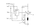
図1に示すように、半導体素子(この場合は、絶縁ゲート形バイポーラトランジスタ(IGBT)は、この素子に接続したゲート・ドライバによって制御する。ゲート・ドライバとしては、予め製作された市販の回路素子が普通使用されるが、ゲート・ドライバは、適当なディスクリートの素子を使って作ることもできる。ゲート・ドライバの主な機能は、半導体スイッチを導通状態へそしてそれに対応して導通状態からへと制御することである。加えて、この制御の後、このドライバは、この素子を制御した先の状態において信頼性良く維持しなければならない。電力消費のため、1つの状態から別の状態へ制御することは、可能な限り素早く行うことが最も有利であり、その理由は、IGBTのような半導体素子における最大の電力損失が、その制御が起きるときに発生するからである。図1のゲート・ドライバは、バイポーラ補助電圧Vcc+, Vcc−を印加する。したがって、素子は、高速に非導通状態にすることができ、そしてさらに、IGBTのエミッタと比べ負のゲートに接続した電圧によりその非導通状態に信頼性良く維持する。これは、この素子が、どのような誘起される電圧および電流パルスによってもターンオンされるのを防止する。
【0007】
補助電圧Vcc+およびVcc−並びにそれらの中間のゼロ電位Comは、ゲート・ドライバのロジック・レベル制御信号On/Offを、この半導体素子の制御を可能にする大きさまで増幅できるようにする。IGBTは、そのゲートGに対し、エミッタEと比べ正の電圧を印加することにより導通状態にすることができる。ゲート・ドライバのゼロ電位は、IGBTエミッタに接続し、したがってゲート・ドライバが、補助電圧Vcc+, Vcc−を使ってターンオンおよびターンオフのために必要な正および負の電圧をそのゲートに供給できるようにする。
本発明によれば、ゲート・ドライバGDのゼロ電位端子と半導体素子のエミッタEとの間には、抵抗器R1と、これに直列接続のダイオードV1を接続し、これら2つは、これらに並列接続した抵抗器R2と、抵抗器R2に直列接続したダイオードV2を有する。さらに、ゲート・ドライバGDのゼロ電位端子と半導体素子のコレクタとの間には、フィードバック・キャパシタC1を接続している。本発明においては、ダイオードV1とV2は、これらを設ける極性により、半導体素子のコレクタ−エミッタ間電圧の変化により生ずるキャパシタC1を通る電流が、この電流の方向に依存して、一時に1つの抵抗器のみを流れることができるようにしている。
【0008】
ターンオン時には、ゲート・ドライバは、その出力に、正の補助電圧Vcc+の大きさの電圧を供給し、この電圧は、通常は+15ボルトであってゲート電流を発生し、これが、IGBTのゲート電圧を、ターンオフ時には通常の−7ボルトの負の補助電圧Vcc−から、素子の約10ボルトのしきい値電圧に向かって増大させる。そのしきい値電圧に達すると、IGBTは、導通状態に移り、そしてそのコレクタ電圧は降下し始める。次に、これは、キャパシタC1と抵抗器R1とダイオードV1を通る電流を発生し、この電流は、抵抗器R1とダイオードV1に電圧損失を生じさせ、これがゲート・ドライバのゼロ電位端子ComをエミッタEに対し負の方向の移動させる。エミッタ電位に対し有効なゲート電圧がしきい値電圧よりも低くなると、ゲート電荷は減少し始め、そしてこれは、コレクタ電圧の変化率が減少することを意味する。このことは、キャパシタC1を通る電流が減少し、R1における電圧損失が低減することを意味する。この電圧損失の程度は、キャパシタC1のキャパシタンス、抵抗器R1の抵抗、およびコレクタ電圧の変化率とに依存する。適当な素子値では、最終的な結果は、コレクタ電圧変化率が、ターンオン・プロセス全体の間に渡ってほとんど一定に留まる。
【0009】
ターンオフ時には、類似のプロセスが生じる。ゲート電圧がしきい値電圧のレベルにまで減少すると、コレクタ電圧は、大きくなり始める。このとき、C1を通る電流は、抵抗器R2とダイオードV2を通るようにされ、そしてこれが抵抗器R2とダイオードV2において生じさせる電圧損失は、ゲート・ドライバのゼロ電位を、エミッタEに対し正の方向に移動させる。R2の抵抗は、通常はR1の抵抗の2倍または3倍の大きさであり、したがって、同じ量の電流により生じる電圧損失もまた、それに対応して大きくなる。より大きな電圧損失が必要であるが、その理由は、しきい値電圧が、正のターンオン電圧よりも負のターンオフ電圧とはより異なっているからである。
【0010】
図1に示した本発明の接続法によれば、抵抗結合1は、2つの逆並列接続した抵抗器R1,R2とダイオードV1,V2の直列接続のものから成っている。この配列により、ゲート電圧の変化を半導体素子のターンオンおよびターンオフのために別々に選択できるようになる。2つの別々の抵抗器をダイオードと一緒に使用することは有利であるが、それは、ターンオンおよびターンオフ時において、最適動作に必要な電圧が通常異なったものとなるからである。ターンオン時においては、ゲート電圧は減少して、このゲート電圧がゲート・ドライバのフルの正補助電圧Vcc+(この値は、通常は+15ボルト)に上昇する前に、素子をターンオンするのに必要なしきい値電圧以下にその電圧を瞬間的に降下させる。ターンオン時には、電流が抵抗器R1とダイオードV1を流れる(ダイオードV1のカソードはフィードバック・キャパシタC1に接続している)。
【0011】
ターンオフ時には、抵抗器R2において生じた電圧降下は、半導体素子のゲートを瞬間的にしきい値電圧よりも上に保つのに使用し、これにより、この素子を所要の変化率でターンオフされるのを可能にする。ターンオフ時において、ゲート電圧は、次にゲート・ドライバの負補助電圧Vcc−(これは通常−7ボルト)と等しくなるようにする。ターンオフにおいて、フィードバック・キャパシタにおける電流の方向は、ターンオン時におけるのと異なっており、したがってダイオードV1,V2は、異なった方向の電流により生じるゲート電圧変化を決めるのに使用することができる。
本発明は、バイポーラ補助電圧を含むゲート・ドライバに関して説明したが、本発明は、ユニポーラ補助電圧を含むゲート・ドライバで実施することも同様に行うことができる。
【0012】
図2は、本発明の1つの好ましい実施形態を示すものであって、ダイオードV1,V2と抵抗器R1,R2は、1つの直列接続をゲート・ドライバのゼロ電位Comから半導体素子の補助エミッタAEへ、そして他方の直列接続をエミッタEへ接続することにより、互いに直列接続している。これら直列接続におけるダイオードの方向は、半導体素子の補助エミッタAEにダイオードV1のアノードが接続し、しかもこれに対応してエミッタEに第2のダイオードV2のカソードが接続するような向きにしている。補助エミッタは、半導体素子の1つの電極であり、そしてこれは、IGBTのような半導体素子の電位を決定するためにのみ通常使用されて、この素子がゲートから信頼性良く制御できるようにする。エミッタは、さらに、エミッタ電流が流れるよう意図した電極である。この補助エミッタとエミッタとは、互いに電気的に直接接続状態にある。図2に示した接続においては、補助エミッタとエミッタとを接続する導体は、エミッタ回路の浮遊インダクタンスLで示している。
【0013】
図2に図示したこの接続法は、図1に示した接続法と全く同じ効果を提供する。得られる追加の利点は、短絡の場合における半導体素子を流れるおそれのある強電流の抑制にある。短絡が発生すると、IGBTのような半導体素子の飽和電圧は、強力に大きくなって、これによりフィードバック・キャパシタC1と抵抗結合1とをさらに作用させてゲート電圧を増加させるようにする。したがって、この好ましい実施形態は、半導体素子のエミッタ回路の浮遊インダクタンスLを用いることによって、短絡時のゲート電圧を減少させ、かつこれにより短絡電流の最大値を穏やかに抑制する。
パワー半導体のエミッタ回路は、常に内部浮遊インダクタンスを含み、エミッタ電流が変化するとき、このインダクタンスにある量の電圧損失が残る。この電圧降下の量は、例えばエミッタ電流の変化率に依存する。図2に示した状況においては、急速に増大する短絡電流がエミッタ回路の浮遊インダクタンスLに電圧損失を生じさせるとき、これは、補助エミッタとエミッタとの間の電圧として示され、エミッタが補助エミッタよりもより負となる。抵抗器R1とR2との間の点もまた、補助エミッタよりもより負となり、これは、半導体素子のゲート電圧に対する基準を与える。
【0014】
また、抵抗器R1とR2との間の点は、ゲート・ドライバのゼロ電位Com、あるいはゲート・ドライバの正および負の電源電圧の共通の中間点であり、これは、ゲート電圧が、補助エミッタ電圧に対し相対的に減少する傾向にあることを意味する。ゲート電圧のこの減少は、素子を流れる電流が抑制されることを意味し、これは、短絡状況においては望ましい結果となる。
当業者には明らかなように、技術の進歩につれ、本発明の基本となる思想は、種々の方法で実施することができる。したがって、本発明並びにその実施形態は、上述の例に制限されるものではなく、特許請求の範囲内で変化し得るものである。
【図面の簡単な説明】
【図1】本発明の制御回路を示す。
【図2】本発明の好ましい実施形態を示す。
【符号の説明】
GD ゲート・ドライバ
E エミッタ
AE 補助エミッタ
C コレクタ
G ゲート
V1,V2 ダイオード
R1,R2 抵抗器
C1 フィードバック・キャパシタ
Com ゼロ電位端子
L 浮遊インダクタンス[0001]
TECHNICAL FIELD OF THE INVENTION
The present invention relates to a control circuit for controlling a semiconductor device including an emitter, a collector and a gate, the control circuit including a gate driver and having its output connected to the gate of the semiconductor device to be controlled. is there.
[0002]
[Prior art]
Currently used power semiconductors, such as IGB transistors, are fast turn-on and turn-off devices, for example, when used in pulse-width-modulated frequency converters, have voltages greater than 10 volts per nanosecond. A rate of change may appear in the output voltage of this frequency converter. Such a rate of change causes considerable distortion to the load of the frequency converter. This frequency converter load is typically a motor, and a high rate of voltage change causes distortion in the winding insulation of the motor and also causes strong voltage reflection in the motor cable. In addition, high rates of change cause electromagnetic interference to radiate to the surroundings.
[0003]
[Problems to be solved by the invention]
It is known that the rate of change of the voltage of a power semiconductor is suppressed by increasing the resistance of a gate resistor connected between the output of a gate driver that controls the semiconductor element and the gate of the semiconductor element to be controlled. I have. This reduces the rate of increase of the gate charge of the power element, thereby causing the gate voltage to increase more slowly. The disadvantage of this connection method is that it depends on the properties of the power elements and their arrangement, which considerably degrades the accuracy of the final result. In addition, the resistance in the coupling unnecessarily increases losses.
It is an object of the present invention to provide a control circuit in which the above disadvantages can be avoided and the semiconductor element can be reliably controlled in a manner independent of this element and using only simple and inexpensive passive elements. It is to provide a control circuit.
[0004]
[Means for Solving the Problems]
This is achieved with the control circuit of the present invention, the control circuit further comprising:
A resistive connection, wherein the two series connections of the diode and the resistor are connected in anti-parallel connection and between the emitter of the semiconductor device and the zero potential of the gate driver;
A feedback capacitor connected between a collector of the semiconductor device and an end of the resistive connection connected to the zero potential of the gate driver;
It is characterized by including.
[0005]
The invention is based on the idea that a change in the collector-emitter voltage of a semiconductor device generates a current through the feedback capacitor C1, which also flows through a resistor coupled to the emitter. The direction of the voltage change determines which of the two resistors the current flows through. In both cases, the current creates a voltage drop across the resistors, which reduces the positive gate voltage of the semiconductor device at turn-on, i.e., when the collector-emitter voltage decreases, and At the time of turn-off, that is, when the collector-emitter voltage increases, the negative gate voltage is reduced. This structure of the control circuit of the invention is fairly simple and therefore cost-effective. Due to this simple structure, the control circuit is also easy to realize and therefore operationally reliable. In addition, losses are significantly lower in a properly sized control circuit, and the operating efficiency of a device utilizing the control circuit of the present invention may be significantly reduced due to the limited voltage increase provided by the circuit. There is no.
Other objects and advantages of the present invention will become apparent from the following description and the appended claims.
[0006]
Embodiment
Hereinafter, the present invention will be described in detail in preferred embodiments and with reference to the accompanying drawings.
As shown in Fig. 1, a semiconductor device (in this case, an insulated gate bipolar transistor (IGBT) is controlled by a gate driver connected to the device. As the gate driver, a commercially available circuit device manufactured in advance is used. Although gate drivers are commonly used, gate drivers can also be made using suitable discrete components.The primary function of a gate driver is to place a semiconductor switch into a conducting state and correspondingly from a conducting state. In addition, after this control, the driver must reliably maintain the element in the state it was in. For power consumption, control from one state to another. It is most advantageous to do as quickly as possible because the largest power loss in semiconductor devices such as
[0007]
The auxiliary voltages Vcc + and Vcc- and the intermediate zero potential Com therebetween enable the logic level control signal On / Off of the gate driver to be amplified to a level that allows control of this semiconductor device. The IGBT can be made conductive by applying a positive voltage to its gate G compared to the emitter E. The zero potential of the gate driver connects to the IGBT emitter, so that the gate driver can use its auxiliary voltages Vcc +, Vcc- to supply its gate with the positive and negative voltages required for turn-on and turn-off. I do.
According to the invention, between the zero potential terminal of the gate driver GD and the emitter E of the semiconductor element, a resistor R1 and a diode V1 connected in series thereto are connected, these two being connected in parallel to these. It has a resistor R2 connected thereto and a diode V2 connected in series with the resistor R2. Further, a feedback capacitor C1 is connected between the zero potential terminal of the gate driver GD and the collector of the semiconductor device. In the present invention, the diodes V1 and V2 have a polarity in which the current flowing through the capacitor C1 caused by a change in the voltage between the collector and the emitter of the semiconductor element depends on the direction of the current. Only vessels can flow.
[0008]
At turn-on, the gate driver supplies at its output a voltage of the order of a positive auxiliary voltage Vcc +, which is typically +15 volts and generates a gate current, which reduces the gate voltage of the IGBT. At turn-off, the voltage is increased from the normal negative auxiliary voltage Vcc- of -7 volts to a threshold voltage of about 10 volts of the device. Upon reaching its threshold voltage, the IGBT goes into conduction and its collector voltage begins to drop. This in turn generates a current through the capacitor C1, the resistor R1 and the diode V1, which causes a voltage loss in the resistor R1 and the diode V1, which connects the gate driver zero potential terminal Com to the emitter. Move E in the negative direction. When the effective gate voltage for the emitter potential falls below the threshold voltage, the gate charge begins to decrease, which means that the rate of change of the collector voltage decreases. This means that the current through the capacitor C1 is reduced and the voltage loss at R1 is reduced. The extent of this voltage loss depends on the capacitance of capacitor C1, the resistance of resistor R1, and the rate of change of the collector voltage. With proper device values, the end result is that the rate of change of the collector voltage remains almost constant during the entire turn-on process.
[0009]
At turn-off, a similar process occurs. As the gate voltage decreases to the level of the threshold voltage, the collector voltage starts to increase. At this time, the current through C1 is made to pass through resistor R2 and diode V2, and the voltage loss it causes in resistor R2 and diode V2 causes the gate driver zero potential to be positive with respect to emitter E, Move in the direction. The resistance of R2 is usually twice or three times as large as the resistance of R1, so the voltage loss caused by the same amount of current is also correspondingly large. Greater voltage loss is required because the threshold voltage is more different for a negative turn-off voltage than for a positive turn-on voltage.
[0010]
According to the connection method according to the invention shown in FIG. 1, the
[0011]
At turn-off, the voltage drop created in resistor R2 is used to momentarily keep the gate of the semiconductor device above the threshold voltage, thereby ensuring that the device is turned off at the required rate of change. enable. At turn-off, the gate voltage is then made to be equal to the gate driver's negative auxiliary voltage Vcc-, which is typically -7 volts. At turn-off, the direction of the current in the feedback capacitor is different than at turn-on, so diodes V1, V2 can be used to determine the gate voltage change caused by the current in the different direction.
Although the invention has been described with reference to a gate driver that includes a bipolar auxiliary voltage, the invention can equally well be implemented with a gate driver that includes a unipolar auxiliary voltage.
[0012]
FIG. 2 shows one preferred embodiment of the invention, in which diodes V1, V2 and resistors R1, R2 connect one series connection from the gate driver zero potential Com to the auxiliary emitter AE of the semiconductor device. , And the other series connection to the emitter E, thereby connecting them in series. The direction of the diodes in these series connections is such that the anode of the diode V1 is connected to the auxiliary emitter AE of the semiconductor element, and the cathode of the second diode V2 is connected to the emitter E correspondingly. The auxiliary emitter is one electrode of a semiconductor device, which is usually only used to determine the potential of a semiconductor device such as an IGBT, so that the device can be reliably controlled from the gate. The emitter is furthermore an electrode intended to carry an emitter current. The auxiliary emitter and the emitter are in direct electrical connection with each other. In the connection shown in FIG. 2, the conductor connecting the auxiliary emitter and the emitter is indicated by the stray inductance L of the emitter circuit.
[0013]
This connection scheme illustrated in FIG. 2 provides exactly the same effect as the connection scheme illustrated in FIG. An additional advantage obtained is in the suppression of strong currents that can flow through the semiconductor element in case of a short circuit. When a short circuit occurs, the saturation voltage of a semiconductor device, such as an IGBT, increases strongly, thereby causing the feedback capacitor C1 and the
The emitter circuit of a power semiconductor always contains an internal stray inductance, and when the emitter current changes, a certain amount of voltage loss remains in this inductance. The amount of this voltage drop depends, for example, on the rate of change of the emitter current. In the situation shown in FIG. 2, when the rapidly increasing short-circuit current causes a voltage loss in the stray inductance L of the emitter circuit, this is indicated as the voltage between the auxiliary emitter and the emitter, and More negative than. The point between resistors R1 and R2 is also more negative than the auxiliary emitter, which provides a reference for the gate voltage of the semiconductor device.
[0014]
Also, the point between resistors R1 and R2 is the gate driver zero potential Com, or the common midpoint between the gate driver's positive and negative supply voltages, where the gate voltage is the auxiliary emitter It means that it tends to decrease relatively to the voltage. This reduction of the gate voltage means that the current flowing through the device is suppressed, which is a desirable result in a short-circuit situation.
As will be apparent to those skilled in the art, as technology advances, the basic idea of the invention can be implemented in a variety of ways. Accordingly, the invention and its embodiments are not limited to the examples described above, but may vary within the scope of the claims.
[Brief description of the drawings]
FIG. 1 shows a control circuit of the present invention.
FIG. 2 shows a preferred embodiment of the present invention.
[Explanation of symbols]
GD Gate driver E Emitter AE Auxiliary emitter C Collector G Gate V1, V2 Diode R1, R2 Resistor C1 Feedback capacitor Com Zero potential terminal L Floating inductance
Claims (3)
抵抗結合(1)であって、ダイオード(V1,V2)と抵抗器(R1,R2)の2つの直列接続を逆並列接続でかつ前記半導体素子(2)のエミッタ(E)と前記ゲート・ドライバ(GD)のゼロ電位(Com)との間に接続した、前記の抵抗結合(1)と、
前記半導体素子(2)のコレクタ(C)と、前記ゲート・ドライバの前記ゼロ電位(Com)に接続した前記抵抗結合(1)の端部との間に接続したフィードバック・キャパシタ(C1)と、
を含むこと、を特徴とする制御回路。A control circuit for controlling a semiconductor device (2) including an emitter (E), a collector (C) and a gate (G), wherein the control circuit includes a gate driver (GD) and controls an output of the gate driver. In the above control circuit connected to the gate (G) of the semiconductor element, the control circuit further comprises:
A resistive coupling (1) in which two series-connected diodes (V1, V2) and resistors (R1, R2) are connected in anti-parallel, and the emitter (E) of the semiconductor device (2) and the gate driver The resistance coupling (1) connected between the (GD) and the zero potential (Com);
A feedback capacitor (C1) connected between a collector (C) of the semiconductor element (2) and an end of the resistance coupling (1) connected to the zero potential (Com) of the gate driver;
A control circuit characterized by including:
Applications Claiming Priority (4)
| Application Number | Priority Date | Filing Date | Title |
|---|---|---|---|
| FI981740A FI105508B (en) | 1998-08-12 | 1998-08-12 | chipset |
| FI981740 | 1998-09-23 | ||
| FI982046 | 1998-09-23 | ||
| FI982046A FI105509B (en) | 1998-08-12 | 1998-09-23 | chipset |
Publications (2)
| Publication Number | Publication Date |
|---|---|
| JP2000089838A JP2000089838A (en) | 2000-03-31 |
| JP3602011B2 true JP3602011B2 (en) | 2004-12-15 |
Family
ID=26160628
Family Applications (1)
| Application Number | Title | Priority Date | Filing Date |
|---|---|---|---|
| JP22772599A Expired - Fee Related JP3602011B2 (en) | 1998-08-12 | 1999-08-11 | Control circuit |
Country Status (6)
| Country | Link |
|---|---|
| US (1) | US6184740B1 (en) |
| EP (1) | EP0980141B1 (en) |
| JP (1) | JP3602011B2 (en) |
| AT (1) | ATE249110T1 (en) |
| DE (1) | DE69910920T2 (en) |
| FI (1) | FI105509B (en) |
Families Citing this family (8)
| Publication number | Priority date | Publication date | Assignee | Title |
|---|---|---|---|---|
| JP5193657B2 (en) * | 2008-04-03 | 2013-05-08 | 日立オートモティブシステムズ株式会社 | Inverter device |
| CA2907472C (en) | 2013-04-04 | 2017-05-02 | Tm4 Inc. | Commutation cell and compensation circuit therefor |
| US9774244B2 (en) * | 2013-11-01 | 2017-09-26 | Tm4 Inc. | Power converter configured for limiting switching overvoltage |
| WO2015070344A1 (en) * | 2013-11-14 | 2015-05-21 | Tm4 Inc. | Compensation circuit, commutation cell and power converter controlling turn-on and turn-off of a power electronic switch |
| CA2930187A1 (en) * | 2013-11-14 | 2015-05-21 | Tm4 Inc. | Commutation cell, power converter and compensation circuit having dynamically controlled voltage gains |
| JP6819256B2 (en) * | 2016-12-07 | 2021-01-27 | 富士電機株式会社 | A drive circuit and a semiconductor module including the circuit |
| FR3115172B1 (en) * | 2020-10-09 | 2024-01-19 | Valeo Siemens Eautomotive Norway As | Electronic circuit for controlling a field effect transistor |
| WO2023157185A1 (en) * | 2022-02-17 | 2023-08-24 | 三菱電機株式会社 | Gate drive circuit and power conversion device |
Family Cites Families (13)
| Publication number | Priority date | Publication date | Assignee | Title |
|---|---|---|---|---|
| JPH01268451A (en) * | 1988-04-15 | 1989-10-26 | Mitsubishi Electric Corp | Overvoltage suppressing circuit for semiconductor device |
| EP0614278B1 (en) | 1988-11-16 | 1998-01-28 | Fuji Electric Co., Ltd. | Drive circuit for use with voltage-driven semiconductor device |
| FR2671241B1 (en) | 1990-12-27 | 1997-04-30 | Peugeot | CONTROL CIRCUIT OF A POWER TRANSISTOR USED IN FORCED SWITCHING. |
| JP3126565B2 (en) * | 1993-11-01 | 2001-01-22 | 株式会社東芝 | AC / DC converter |
| FR2713029B1 (en) * | 1993-11-22 | 1995-12-29 | Gec Alsthom Transport Sa | Power switch control circuit supply device. |
| JPH0829725A (en) | 1994-05-10 | 1996-02-02 | Canon Inc | Compound-eye image display device |
| SE9500761D0 (en) | 1995-03-02 | 1995-03-02 | Abb Research Ltd | Protection circuit for series-connected power semiconductors |
| JP3125622B2 (en) | 1995-05-16 | 2001-01-22 | 富士電機株式会社 | Semiconductor device |
| JP3373704B2 (en) * | 1995-08-25 | 2003-02-04 | 三菱電機株式会社 | Insulated gate transistor drive circuit |
| EP0814564A1 (en) | 1996-06-20 | 1997-12-29 | ANSALDO INDUSTRIA S.p.A. | Electronic switching circuit with reduction of switching transients |
| WO1998001940A1 (en) | 1996-07-05 | 1998-01-15 | Hitachi, Ltd. | Power converter |
| SE515457C2 (en) * | 1996-09-20 | 2001-08-06 | Abb Research Ltd | Method and device for power transistor |
| JP3067687B2 (en) * | 1997-05-08 | 2000-07-17 | 富士電機株式会社 | IGBT drive circuit |
-
1998
- 1998-09-23 FI FI982046A patent/FI105509B/en not_active IP Right Cessation
-
1999
- 1999-07-19 US US09/357,240 patent/US6184740B1/en not_active Expired - Lifetime
- 1999-07-23 EP EP99660126A patent/EP0980141B1/en not_active Expired - Lifetime
- 1999-07-23 DE DE69910920T patent/DE69910920T2/en not_active Expired - Lifetime
- 1999-07-23 AT AT99660126T patent/ATE249110T1/en not_active IP Right Cessation
- 1999-08-11 JP JP22772599A patent/JP3602011B2/en not_active Expired - Fee Related
Also Published As
| Publication number | Publication date |
|---|---|
| US6184740B1 (en) | 2001-02-06 |
| ATE249110T1 (en) | 2003-09-15 |
| EP0980141B1 (en) | 2003-09-03 |
| DE69910920D1 (en) | 2003-10-09 |
| FI982046L (en) | 2000-02-13 |
| FI105509B (en) | 2000-08-31 |
| EP0980141A1 (en) | 2000-02-16 |
| DE69910920T2 (en) | 2004-07-22 |
| FI982046A0 (en) | 1998-09-23 |
| JP2000089838A (en) | 2000-03-31 |
Similar Documents
| Publication | Publication Date | Title |
|---|---|---|
| US10164550B2 (en) | Method, circuit configuration and bridge circuit for charging a capacitance effective on main current terminals of semiconductor switch | |
| CN101079576B (en) | System for providing switching to a power regulator | |
| KR0140227B1 (en) | Electronic control circuits electronically commutated motor systems | |
| US7830196B2 (en) | Semiconductor device alleviating or preventing surge voltage | |
| CN113098469A (en) | Time programmable fail safe pull-down circuit for GaN switch | |
| US4356416A (en) | Voltage controlled non-saturating semiconductor switch and voltage converter circuit employing same | |
| US6909620B2 (en) | Inverter configurations with shoot-through immunity | |
| US7701279B2 (en) | Driving circuit for an emitter-switching configuration | |
| CN111865086B (en) | Self-powered control circuit and control method and switching power supply circuit | |
| US7660094B2 (en) | Inverter circuit | |
| US20170346480A1 (en) | High-Voltage Stacked Transistor Circuit | |
| US4547686A (en) | Hybrid power semiconductor switch | |
| JP2023516357A (en) | Drive circuits and drive systems for power devices | |
| US6229356B1 (en) | Stabilized gate drivers | |
| US5570057A (en) | Three-terminal insulated-gate power electronic device with a variable-slope saturated output characterisitic depending in a discontinuous way on the output current | |
| US7248093B2 (en) | Bipolar bootstrap top switch gate drive for half-bridge semiconductor power topologies | |
| US7019579B2 (en) | Circuit arrangement for rapidly controlling in particular inductive loads | |
| JP3602011B2 (en) | Control circuit | |
| CN115021534A (en) | A gate driver circuit, power supply circuit and method | |
| EP3764527B1 (en) | Switching device and method for controlling switching device | |
| JP4110052B2 (en) | Inverter circuit | |
| US20080197904A1 (en) | Circuit Arrangement for Switching a Load | |
| GB2053606A (en) | Improvements in and relating to semiconductor switching circuits | |
| JP2001169534A (en) | Gate circuit of insulated gate type semiconductor device | |
| JP7717019B2 (en) | Semiconductor Devices |
Legal Events
| Date | Code | Title | Description |
|---|---|---|---|
| TRDD | Decision of grant or rejection written | ||
| A01 | Written decision to grant a patent or to grant a registration (utility model) |
Free format text: JAPANESE INTERMEDIATE CODE: A01 Effective date: 20040907 |
|
| A61 | First payment of annual fees (during grant procedure) |
Free format text: JAPANESE INTERMEDIATE CODE: A61 Effective date: 20040921 |
|
| R150 | Certificate of patent or registration of utility model |
Free format text: JAPANESE INTERMEDIATE CODE: R150 |
|
| FPAY | Renewal fee payment (event date is renewal date of database) |
Free format text: PAYMENT UNTIL: 20071001 Year of fee payment: 3 |
|
| FPAY | Renewal fee payment (event date is renewal date of database) |
Free format text: PAYMENT UNTIL: 20081001 Year of fee payment: 4 |
|
| FPAY | Renewal fee payment (event date is renewal date of database) |
Free format text: PAYMENT UNTIL: 20091001 Year of fee payment: 5 |
|
| FPAY | Renewal fee payment (event date is renewal date of database) |
Free format text: PAYMENT UNTIL: 20101001 Year of fee payment: 6 |
|
| FPAY | Renewal fee payment (event date is renewal date of database) |
Free format text: PAYMENT UNTIL: 20101001 Year of fee payment: 6 |
|
| FPAY | Renewal fee payment (event date is renewal date of database) |
Free format text: PAYMENT UNTIL: 20111001 Year of fee payment: 7 |
|
| FPAY | Renewal fee payment (event date is renewal date of database) |
Free format text: PAYMENT UNTIL: 20111001 Year of fee payment: 7 |
|
| FPAY | Renewal fee payment (event date is renewal date of database) |
Free format text: PAYMENT UNTIL: 20121001 Year of fee payment: 8 |
|
| FPAY | Renewal fee payment (event date is renewal date of database) |
Free format text: PAYMENT UNTIL: 20131001 Year of fee payment: 9 |
|
| R250 | Receipt of annual fees |
Free format text: JAPANESE INTERMEDIATE CODE: R250 |
|
| R250 | Receipt of annual fees |
Free format text: JAPANESE INTERMEDIATE CODE: R250 |
|
| R250 | Receipt of annual fees |
Free format text: JAPANESE INTERMEDIATE CODE: R250 |
|
| LAPS | Cancellation because of no payment of annual fees |