EP2989700B1 - Schaltungsanordnung zum überspannungsschutz in gleichstrom-versorgungskreisen - Google Patents
Schaltungsanordnung zum überspannungsschutz in gleichstrom-versorgungskreisen Download PDFInfo
- Publication number
- EP2989700B1 EP2989700B1 EP14713824.2A EP14713824A EP2989700B1 EP 2989700 B1 EP2989700 B1 EP 2989700B1 EP 14713824 A EP14713824 A EP 14713824A EP 2989700 B1 EP2989700 B1 EP 2989700B1
- Authority
- EP
- European Patent Office
- Prior art keywords
- gas discharge
- arresters
- voltage
- diodes
- spark gaps
- Prior art date
- Legal status (The legal status is an assumption and is not a legal conclusion. Google has not performed a legal analysis and makes no representation as to the accuracy of the status listed.)
- Not-in-force
Links
- 239000003990 capacitor Substances 0.000 claims description 16
- 230000003213 activating effect Effects 0.000 claims 1
- 238000010295 mobile communication Methods 0.000 claims 1
- 239000004020 conductor Substances 0.000 description 4
- 238000002485 combustion reaction Methods 0.000 description 2
- 238000001816 cooling Methods 0.000 description 1
- 238000012217 deletion Methods 0.000 description 1
- 230000037430 deletion Effects 0.000 description 1
- 230000001419 dependent effect Effects 0.000 description 1
- 238000011161 development Methods 0.000 description 1
- 230000018109 developmental process Effects 0.000 description 1
- 238000010586 diagram Methods 0.000 description 1
- 238000010791 quenching Methods 0.000 description 1
- 230000000171 quenching effect Effects 0.000 description 1
Images

Classifications
-
- H—ELECTRICITY
- H01—ELECTRIC ELEMENTS
- H01T—SPARK GAPS; OVERVOLTAGE ARRESTERS USING SPARK GAPS; SPARKING PLUGS; CORONA DEVICES; GENERATING IONS TO BE INTRODUCED INTO NON-ENCLOSED GASES
- H01T4/00—Overvoltage arresters using spark gaps
- H01T4/16—Overvoltage arresters using spark gaps having a plurality of gaps arranged in series
-
- H—ELECTRICITY
- H01—ELECTRIC ELEMENTS
- H01T—SPARK GAPS; OVERVOLTAGE ARRESTERS USING SPARK GAPS; SPARKING PLUGS; CORONA DEVICES; GENERATING IONS TO BE INTRODUCED INTO NON-ENCLOSED GASES
- H01T4/00—Overvoltage arresters using spark gaps
- H01T4/02—Details
-
- H—ELECTRICITY
- H01—ELECTRIC ELEMENTS
- H01T—SPARK GAPS; OVERVOLTAGE ARRESTERS USING SPARK GAPS; SPARKING PLUGS; CORONA DEVICES; GENERATING IONS TO BE INTRODUCED INTO NON-ENCLOSED GASES
- H01T4/00—Overvoltage arresters using spark gaps
- H01T4/16—Overvoltage arresters using spark gaps having a plurality of gaps arranged in series
- H01T4/20—Arrangements for improving potential distribution
Definitions
- the invention relates to a circuit arrangement for overvoltage protection in DC supply circuits of electronic components or devices, in particular devices for telecommunications, such as transmitting and receiving antennas and / or mobile systems consisting of a coarse protection series circuit of spark gaps or gas discharge between the input terminals and parallel to the spark gaps or gas discharge dischargers switched capacitors, at least one fine protection element between the output terminals and a decoupling impedance between coarse protection series circuit and fine protection element, according to the preamble of claim 1.
- the arc-burning voltage is brought by series connection of the partial spark gaps to n times the arc voltage of a partial spark gap.
- the partial spark gaps with the exception of the first partial spark gap responding in the lightning current event case are connected by impedances with the goal that a successive switching through takes place.
- the second and all other spark gaps after DE 297 24 817 U1 are directly connected to a common reference potential, in particular to the free electrode of the last spark gap as a reference electrode.
- overvoltage protection devices called "Blitzduktor" DEHN + S ⁇ HNE GmbH + Co. KG, Neu here, Germany.
- Such overvoltage arresters BVD KKS ALD 75 or BVT ALD 36 have series-connected gas discharge arresters with capacitors connected in parallel for the purpose of a successive switching through of the individual gas discharge arresters.
- the aim of the known arrester is to reduce the response voltage between the wires of a double wire.
- addition of the arc voltage is achieved by the series connection of the spark gaps or gas discharge, so that an increase in the allowable operating voltage is given. If the sum of the arc burn voltages of the individual components is above the operating voltage, erase, i. switching off the arresters independently of the current flowing in the event of the arresters being activated.
- JP 2002 010484 A discloses an overvoltage protection circuit consisting of a series arrangement of arresters, a fine protection element, a decoupling impedance and capacitors.
- the capacitors (capacitors) connected in parallel with the gas discharge arresters provide voltage division control, with the result that the gas discharge conductors are switched through sequentially. As a result, an overall response voltage of the circuit arrangement is achieved, which corresponds to the response voltage of a single gas discharge arrester.
- the design of the downstream, located on the output terminal fine protection circuit is placed on the arc voltage of the overall arrangement.
- a very low decoupling impedance for coordinating the overall arrangement of coarse protection to fine protection can be used, since it is only necessary to ensure that in the current increase before reaching the load limit of inserted diodes as a fine protection element, a sufficient voltage drop is created to switch on the gas discharge arresters.
- the required current carrying capacity of the fine protection is reduced by the intended function of the sequential switching of the coarse protection elements, i. the gas discharge tube or the spark gaps.
- the decoupling impedance can be designed for high operating currents in view of the low impedance values.
- a circuit arrangement for overvoltage protection in DC power supply circuits of electronic components or devices, in particular telecommunications equipment, such as transmitting and receiving antennas and / or mobile devices consisting of a coarse protection series connection of spark gaps or gas discharge between the input terminals and capacitors connected in parallel with the spark gaps or gas discharge conductors.
- at least one fine protection element is arranged between the output terminals and there is a decoupling impedance between the coarse protection series circuit and the fine protection element.
- the capacitance values of the capacitors are many times greater than the capacitance values of the gas discharge arresters or spark gaps.
- the inductance of the decoupling impedance is designed so that a sufficient voltage drop results in the current increase case, in order to switch the spark gaps or gas discharge arresters before the load limit of the fine protection element is reached.
- a capacitor is connected between each connection point of the spark gaps or gas discharge conductors and the earth potential, the ratio of the capacitance values of the gas discharge conductor and the spark gap to the capacitor being substantially 1: 100.
- the gas discharge arresters have a substantially equal response voltage, so that in the event of an overvoltage, a sequential switching through of the gas discharge arresters can take place.
- the fine protection element consists in a preferred embodiment of a series circuit of diodes.
- suppressor diodes or TVS diodes are used here.
- the stand-off voltage of these diodes of the series connection is greater than the sum of the arc voltage of the gas discharge tube.
- the Fig. 1 first lets you recognize the input terminals -V DC and + V DC. Between these input terminals is a series connection of eg five gas discharge arresters A1 to A5. The series connection of these five gas discharge arresters ensures that the arc burning voltage is approximately 60 V. It is thereby achieved extinguishing the gas discharge tube independent of the operating current at operating voltages up to 60 V.
- the capacitors C1 to C4 are connected to ground potential and to the + V DC terminal, respectively.
- the capacitance values of these capacitors are, for example, 100 times the capacitance of the gas discharge arresters. This ensures that initially the pending input voltage is applied completely to the gas discharge tube A5.
- the gas discharge arrester A5 is thereforeteurgeschaitet when exceeding a specified threshold voltage.
- gas discharge arresters A1 to A5 are used with approximately the same response voltage, a sequential switching through of the gas discharge arresters A5 to A1 occurs.
- the fine protection level is realized by an opposite pole series connection of suppressor or TVS diodes V1 to V4, wherein for the dimensioning of the fine protection, consisting of the diodes V1 to V4, the selected state off-voltage of the diodes higher than the sum of the arc voltage of the arrester A1 to A5 is. As a result, the diodes V1 to V4 are relieved after response of the arrester A5 to A1.
- the inductance of the coil L1 is to be chosen so that in the current increase before reaching the load limit of the diodes V1 to V4 sufficient voltage drop occurs at L1 to turn on the gas discharge arresters A1 to A4.
- the exemplary circuit after Fig. 1 was dimensioned for a likewise exemplary operating voltage of 60 V DC.
- the gas discharge arresters A1 to A5 have a maximum response voltage of 500 V (1 kV / ⁇ s).
- the capacitance of the capacitors C1 to C4 is about 10 nF.
- the capacity of the gas discharge tube is approx. 1.5 pF.
- the TVS diodes V1 to V4 have a stand-off voltage of 30V.
- the maximum current carrying capacity is 250 A (10/350 ⁇ s).
- the maximum clamping voltage is 100 V.
Landscapes
- Emergency Protection Circuit Devices (AREA)
Description
- Die Erfindung betrifft eine Schaltungsanordnung zum Überspannungsschutz in Gleichstrom-Versorgungskreisen von elektronischen Komponenten oder Geräten, insbesondere Geräten zur Telekommunikation, wie Sende- und Empfangsantennen und/oder Mobilfunkanlagen, bestehend aus einer Grobschutz-Reihenschaltung von Funkenstrecken oder Gasentladungsableitern zwischen den Eingangsklemmen sowie parallel zu den Funkenstrecken oder Gasentladungsableitern geschalteten Kondensatoren, mindestens einem Feinschutzelement zwischen den Ausgangsklemmen und einer Entkopplungsimpedanz zwischen Grobschutz-Reihenschaltung und Feinschutzelement, gemäß Oberbegriff des Anspruchs 1.
- Aus der
DE 25 47 604 A1 ist eine Steuerungsanordnung für die Funkenstrecken eines Überspannungsableiters vorbekannt. Dortige parallel zu den Funkenstrecken geschaltete Steuerwiderstände sind in der Lage, den Spannungsabfall über die einzelnen Funkenstrecken so zu beeinflussen, dass zunächst eine erste Funkenstrecke zündet. Durch Steuerwiderstände mit verschieden großen Exponenten kann ein nacheinander folgendes Schalten der weiteren Funkenstrecken erfolgen, um die Ansprechspannung der Gesamtanordnung zu reduzieren. Mit der Lösung nachDE 25 47 604 A1 soll der Nachteil des Wiederzündens reduziert werden, der bei bis dahin bekannten Anordnungen eintrat, wenn mehrere Überspannungsvorgänge kurz hintereinander folgen, so dass die Abkühlung der Funkenstrecken zwischen den einzelnen Überspannungsschutzvorgängen nicht ausreichend ist. - Bei der blitzstromtragfähigen Funkenstrecke nach
DE 297 24 817 U1 wird von mehreren, in Reihe geschalteten Funkenstrecken ausgegangen, wobei die Funkenstrecke aus n-Teilfunkenstrecken besteht, deren Lichtbogenbrennspannung durch Reihenschaltung der Teilfunkenstrecken auf den n-fachen Wert der Lichtbogenbrennspannung einer Teilfunkenstrecke gebracht ist. Die Teilfunkenstrecken mit Ausnahme der im Blitzstrom-Ereignisfall ersten ansprechenden Teilfunkenstrecke sind durch Impedanzen geschaltet mit dem Ziel, dass ein sukzessives Durchschalten erfolgt. Die zweite und alle weiteren Funkenstrecken nachDE 297 24 817 U1 sind direkt an ein gemeinsames Bezugspotential, insbesondere an die freie Elektrode der letzten Funkenstrecke als Bezugselektrode gelegt. - Bekannt sind weiterhin Überspannungsschutzgeräte der Bezeichnung "Blitzduktor" der Firma DEHN + SÖHNE GmbH + Co. KG, Neumarkt, Deutschland. Derartige Überspannungsschutzgeräte Blitzduktor BVT KKS ALD 75 oder BVT ALD 36 weisen in Reihe geschaltete Gasentladungsableiter mit parallel geschalteten Kondensatoren auf zum Zweck eines sukzessiven Durchschaltens der einzelnen Gasentladungsableiter. Ziel der vorbekannten Ableiter ist es, die Ansprechspannung zwischen den Adern einer Doppelader zu reduzieren. Bei den bekannten Überspannungsschutzgeräten wird durch die Reihenschaltung der Funkenstrecken bzw. Gasentladungsableiter eine Addition der Bogenbrennspannung erreicht, so dass eine Erhöhung der zulässigen Betriebsspannung gegeben ist. Liegt die Summe der Bogenbrennspannungen der einzelnen Komponenten oberhalb der Betriebsspannung, erfolgt ein Löschen, d.h. ein Ausschalten der Ableiter unabhängig vom im Fall des Ansprechens der Ableiter fließenden Strom.
-
JP 2002 010484 A - Aus dem Vorgenannten ist es Aufgabe der Erfindung, eine weiterentwickelte Schaltungsanordnung zum Überspannungsschutz in Gleichstrom-Versorgungskreisen von elektronischen Komponenten oder Geräten, insbesondere Geräten der Mobilfunktechnik anzugeben, welche sicherstellt, dass der erforderliche Überspannungsschutz unabhängig vom Betriebsstrom bzw. Nennstrom gegeben ist. Diesbezüglich wird auf den an sich bekannten Gedanken der Reihenschaltung von Gasableitern zurückgegriffen und eine damit erreichte Addition der Bogenbrennspannung genutzt, so dass ein Löschen bei höheren Nennspannungen möglich ist. Die erfindungsgemäße Lösung soll einen niedrigen Schutzpegel von ≤ 100 V gewährleisten, um die Eingangsschaltung von Stromversorgungen oder aber von Antennen bzw. Verstärkern bei Mobilfunkanlagen zu sichern. Insofern soll die zu schaffende Schaltung einen Überspannungsschutz für unterschiedliche Komponenten ermöglichen, um den installationsseitigen und kostenseitigen Aufwand zu reduzieren.
- Die Lösung der Aufgabe der Erfindung erfolgt durch die Merkmalskombination nach Anspruch 1, wobei die Unteransprüche mindestens zweckmäßige Ausgestaltungen und Weiterbildungen darstellen,
- Durch die Reihenschaltung von Gasentladungsableitern oder Funkenstrecken und die damit erreichte Addition der einzelnen Bogenbrennspannungen wird erfindungsgemäß ein Löschen für Betriebsspannungen bis zur Summe der Bogenbrennspannung erreicht, ohne dass eine Einschränkung der Schaltungsanordnung auf einen maximalen Betriebsstrom oder Fehlerstrom vorliegt.
- Durch die parallel zu den Gasentladungsableitern geschalteten Kapazitäten (Kondensatoren) wird eine Steuerung der Spannungsaufteilung erreicht mit der Folge, dass die Gasentladungsableiter sequenziell durchschalten. Hierdurch wird eine Gesamtansprechspannung der Schaltungsanordnung erreicht, die der Ansprechspannung eines einzelnen Gasentladungsableiters entspricht.
- Die Auslegung der nachgeordneten, an der Ausgangsklemme befindlichen Feinschutzschaltung ist auf die Bogenbrennspannung der Gesamtanordnung abgestellt.
- Erfindungsgemäß kann eine sehr niedrige Entkopplungsimpedanz zur Koordination der Gesamtanordnung Grobschutz zu Feinschutz zur Anwendung kommen, da lediglich dafür zu sorgen ist, dass im Stromanstieg vor Erreichen der Belastungsgrenze eingesetzter Dioden als Feinschutzelement ein ausreichender Spannungsabfall entsteht, um die Gasentladungsableiter durchzuschalten. Im Übrigen reduziert sich die notwendige Stromtragfähigkeit des Feinschutzes durch die angestrebte Funktion des sequenziellen Durchschaltens der Grobschutzelemente, d.h. der Gasentladungsableiter oder der Funkenstrecken. Die Entkopplungsimpedanz kann mit Blick auf die niedrigen Impedanzwerte auf hohe Betriebsströme ausgelegt werden.
- Es wird also demnach von einer Schaltungsanordnung zum Überspannungsschutz in Gleichstrom-Versorgungskreisen von elektronischen Komponenten oder Geräten, insbesondere Geräten zur Telekommunikation, wie Sende- und Empfangsantennen und/oder Mobilfunkanlagen ausgegangen, bestehend aus einer Grobschutz-Reihenschaltung von Funkenstrecken oder Gasentladungsableitern zwischen den Eingangsklemmen sowie parallel zu den Funkenstrecken oder Gasentladungsableitern geschalteten Kondensatoren. Weiterhin ist mindestens ein Feinschutzelement zwischen den Ausgangsklemmen angeordnet und es ist eine Entkopplungsimpedanz zwischen der Grobschutz-Reihenschaltung und dem Feinschutzelement vorhanden.
- Erfindungsgemäß sind die Kapazitätswerte der Kondensatoren um ein Vielfaches größer als die Kapazitätswerte der Gasentladungsableiter oder Funkenstrecken. Wie bereits erwähnt, ist die Induktivität der Entkopplungsimpedanz so ausgelegt, dass im Stromanstiegsfall ein ausreichender Spannungsabfall resultiert, um die Funkenstrecken oder Gasentladungsableiter durchzuschalten, bevor die Belastungsgrenze des Feinschutzelements erreicht ist.
- Ausgestaltend ist zwischen jedem Verbindungspunkt der Funkenstrecken oder Gasentladungsableiter und dem Erdpotential ein Kondensator geschaltet, wobei das Verhältnis der Kapazitätswerte Gasentladungsableiter bzw. Funkenstrecke zu Kondensator bei im Wesentlichen 1:100 liegt.
- Die Gasentladungsableiter besitzen eine im Wesentlichen gleiche Ansprechspannung, so dass im Überspannungsfall ein sequenzielles Durchschalten der Gasentladungsableiter erfolgen kann.
- Das Feinschutzelement besteht bei einer bevorzugten Ausführungsform aus einer Reihenschaltung von Dioden. Hier kommen insbesondere Suppressordioden bzw. TVS-Dioden zum Einsatz. Die Stand Off-Spannung dieser Dioden der Reihenschaltung ist dabei größer als die Summe der Bogenbrennspannungen der Gasentladungsableiter.
- Die Erfindung soll nachstehend anhand eines Ausführungsbeispiels sowie von Figuren näher erläutert werden.
- Hierbei zeigen:
- Fig. 1
- eine beispielhafte Schaltungsanordnung für eine Betriebsspannung bis 60 V DC und
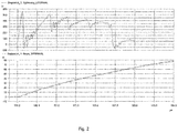
- Fig. 2
- ein Diagramm des sequenziellen Durchschaltens der Gasentladungsableiter A1 bis A5 nach
Fig. 1 sowie den diesbezüglichen Stromverlauf über der Zeit. - Die
Fig. 1 lässt zunächst die Eingangsklemmen -V DC und +V DC erkennen. Zwischen diesen Eingangsklemmen befindet sich eine Reihenschaltung aus z.B. fünf Gasentladungsableitern A1 bis A5. Durch die Reihenschaltung dieser fünf Gasentladungsableiter wird erreicht, dass die Bogenbrennspannung bei ca. 60 V liegt. Es wird hierdurch ein Löschen der Gasentladungsableiter unabhängig vom Betriebsstrom bei Betriebsspannungen bis 60 V erreicht. - An den Verbindungspunkten der Gasentladungsableiter A1 bis A5 sind die Kondensatoren C1 bis C4 gegen Erdpotential bzw. gegen die +V DC-Klemme geschaltet. Die Kapazitätswerte dieser Kondensatoren liegen beispielsweise bei dem 100-fachen der Kapazität der Gasentladungsableiter. Hierdurch wird erreicht, dass zunächst die anstehende Eingangsspannung vollständig am Gasentladungsableiter A5 anliegt. Der Gasentladungsableiter A5 wird daher beim Überschreiten eines spezifizierten Ansprechspannung durchgeschaitet.
- Danach liegt die Eingangsspannung an der verbleibenden Anordnung A1 bis A4. Die weitere Spannungsaufteilung ergibt sich durch die Kapazität von A4 und C3, wobei das gleiche Verhältnis gilt wie bei A5 zu C4.
- Werden Gasentladungsableiter A1 bis A5 mit annähernd gleicher Ansprechspannung verwendet, stellt sich ein sequenzielles Durchschalten der Gasentladungsableiter A5 bis A1 ein.
- Die Feinschutzstufe wird durch eine gegenpolige Reihenschaltung von Suppressor- oder TVS-Dioden V1 bis V4 realisiert, wobei für die Dimensionierung des Feinschutzes, bestehend aus den Dioden V1 bis V4, die gewählte Stand Off-Spannung der Dioden höher als die Summe der Bogenbrennspannungen der Ableiter A1 bis A5 ist. Hierdurch werden die Dioden V1 bis V4 nach Ansprechen der Ableiter A5 bis A1 entlastet.
- Zwischen der Eingangsklemme -V DC und der Ausgangsklemme -V DC (mit internal gekennzeichnet) befindet sich noch eine Entkopplungsimpedanz L1.
- Die Induktivität der Spule L1 ist dabei so zu wählen, dass im Stromanstieg vor Erreichen der Belastungsgrenze der Dioden V1 bis V4 ein ausreichender Spannungsabfall an L1 entsteht, um die Gasentladungsableiter A1 bis A4 durchzuschalten.
- Hier gilt folgender Zusammenhang:

- Die beispielhafte Schaltung nach
Fig. 1 wurde für eine ebenfalls beispielhafte Betriebsspannung von 60 V DC dimensioniert. - Dabei ergibt sich folgende beispielhafte Auslegung.
- Die Gasentladungsableiter A1 bis A5 weisen eine maximale Ansprechspannung von 500 V (1 kV/µs) auf. Die Kapazität der Kondensatoren C1 bis C4 liegt bei ca. 10 nF. Die Kapazität der Gasentladungsableiter liegt bei ca. 1,5 pF.
- Die TVS-Dioden V1 bis V4 weisen eine Stand Off-Spannung von 30 V auf. Die maximale Strombelastbarkeit beträgt 250 A (10/350 µs). Die maximale Clamping Voltage liegt bei 100 V.
- Die Induktivität L1 ergibt sich bei einer anzunehmenden Stromsteilheit dI/dt = 250 A/10 µs : 25 A/µs. Der notwendige Spannungsabfall über L1 liegt bei 500 V - 100 V = 400 V. Damit ergibt sich

- Selbstverständlich ist eine adäquate Auslegung für andere Betriebsspannungen und andere Basiswerte der Kapazität von Gasentladungsableitern möglich, ohne den Erfindungsgedanken zu verlassen.
Claims (4)
- Schaltungsanordnung zum Überspannungsschutz in Gleichstrom-Versorgungskreisen von elektronischen Komponenten oder Geräten, insbesondere Geräten zur Telekommunikation wie Sende- und Empfangsantennen und/oder Mobilfunkanlagen, bestehend aus einer Grobschutz-Reihenschaltung von Funkenstrecken oder Gasentladungsableitern (A1 - A5) zwischen den Eingangsklemmen sowie parallel zu den Funkenstrecken oder Gasentladungsableitern (A1 - A5) geschalteten Kondensatoren (C1 - C4), mindestens einem Feinschutzelement (V1 - V4) zwischen den Ausgangsklemmen und einer Entkopplungsimpedanz (L1) zwischen der Grobschutz-Reihenschaltung und dem Feinschutzelement, wobei die Kapazitätswerte der Kondensatoren (C1 - C4) um ein Vielfaches größer als die Kapazitätswerte der Gasentladungsableiter oder Funkenstrecken (A1 - A5) sind und zwischen jedem Verbindungspunkt der Funkenstrecken oder Gasentladungsableiter (A1 - A5) und Erdpotential ein Kondensator (C1 - C4) geschaltet ist, wobei das Verhältnis der Kapazitätswerte Gasentladungsableiter oder Funkenstrecke zu Kondensator bei im Wesentlichen 1:100 liegt sowie die Induktivität der Entkopplungsimpedanz (L1) so ausgelegt ist, dass im Stromanstiegsfall ein ausreichender Spannungsabfall entsteht, um die Funkenstrecken oder Gasentladungsableiter (A1 - A5) durchzuschalten, bevor die Belastungsgrenze des Feinschutzelements (V1 -V4) erreicht ist, wobei die Auslegung der Entkopplungsimpedanz (L1) nach der Beziehung

- Schaltungsanordnung nach Anspruch 1,
dadurch gekennzeichnet, dass
die Gasentladungsableiter (A1 - A5) eine im Wesentlichen gleiche Ansprechspannung besitzen, so dass im Überlastfall ein sequenzielles Durchschalten der Gasentladungsableiter erfolgt. - Schaltungsanordnung nach einem der vorangegangenen Ansprüche, dadurch gekennzeichnet, dass
das Feinschutzelement aus einer Reihenschaltung von Dioden (V1 -V4) besteht. - Schaltungsanordnung nach Anspruch 3,
dadurch gekennzeichnet, dass
die Dioden (V1 - V4) als Suppressordioden oder TVS-Dioden ausgebildet sind und die Stand Off-Spannung der Dioden der Reihenschaltung größer als die Summe der Bogenbrennspannung der Ableiter (A1 - A5) ist.
Applications Claiming Priority (2)
| Application Number | Priority Date | Filing Date | Title |
|---|---|---|---|
| DE202013101705U DE202013101705U1 (de) | 2013-04-22 | 2013-04-22 | Schaltungsanordnung zum Überspannungsschutz in Gleichstrom-Versorgungskreisen |
| PCT/EP2014/056168 WO2014173613A1 (de) | 2013-04-22 | 2014-03-27 | Schaltungsanordnung zum überspannungsschutz in gleichstrom-versorgungskreisen |
Publications (2)
| Publication Number | Publication Date |
|---|---|
| EP2989700A1 EP2989700A1 (de) | 2016-03-02 |
| EP2989700B1 true EP2989700B1 (de) | 2019-02-20 |
Family
ID=48576138
Family Applications (1)
| Application Number | Title | Priority Date | Filing Date |
|---|---|---|---|
| EP14713824.2A Not-in-force EP2989700B1 (de) | 2013-04-22 | 2014-03-27 | Schaltungsanordnung zum überspannungsschutz in gleichstrom-versorgungskreisen |
Country Status (5)
| Country | Link |
|---|---|
| US (1) | US20160094018A1 (de) |
| EP (1) | EP2989700B1 (de) |
| CN (1) | CN105122562A (de) |
| DE (1) | DE202013101705U1 (de) |
| WO (1) | WO2014173613A1 (de) |
Families Citing this family (5)
| Publication number | Priority date | Publication date | Assignee | Title |
|---|---|---|---|---|
| CN104300521A (zh) * | 2013-07-16 | 2015-01-21 | 中国电信股份有限公司 | 带续流遮断功能的电源防雷装置 |
| DE102015200186A1 (de) * | 2015-01-09 | 2016-07-14 | Osram Gmbh | Überspannungsschutzvorrichtung sowie Leuchte mit einer derartigen Überspannungsschutzvorrichtung |
| CN110971115B (zh) * | 2018-09-29 | 2023-08-29 | 中兴通讯股份有限公司 | 雷击浪涌防护电路、方法、系统、存储介质及电子装置 |
| CN111524536B (zh) * | 2019-02-01 | 2023-09-08 | 富士通株式会社 | 信号处理方法和信息处理设备 |
| CN110071494A (zh) * | 2019-06-04 | 2019-07-30 | 深圳市槟城电子有限公司 | 一种防护电路和电子设备 |
Family Cites Families (7)
| Publication number | Priority date | Publication date | Assignee | Title |
|---|---|---|---|---|
| US3934175A (en) * | 1973-12-03 | 1976-01-20 | General Semiconductor Industries, Inc. | Power surge protection system |
| DE2547604B2 (de) | 1975-10-24 | 1980-07-31 | Licentia Patent-Verwaltungs-Gmbh, 6000 Frankfurt | Steuerungsanordnung für die Funkenstrecken eines Überspannungsabieiters |
| DE29724817U1 (de) | 1997-12-11 | 2004-04-29 | Obo Bettermann Gmbh & Co. Kg | Blitzstromtragfähige Funkenstrecke |
| JP2002010484A (ja) * | 2000-06-16 | 2002-01-11 | Ntt Docomo Kyushu Inc | サージ吸収装置 |
| TR200402439T4 (tr) * | 2002-04-11 | 2004-12-21 | Obo Bettermann Gmbh & Co. Kg. | Kıvılcım aralığı. |
| JP3854305B1 (ja) * | 2005-12-09 | 2006-12-06 | 均 木嶋 | 過電圧防護器、過電圧防護方法 |
| US8400744B2 (en) * | 2010-05-19 | 2013-03-19 | Schneider Electric USA, Inc. | Earth leakage detection module with robust transient suppression |
-
2013
- 2013-04-22 DE DE202013101705U patent/DE202013101705U1/de not_active Expired - Lifetime
-
2014
- 2014-03-27 WO PCT/EP2014/056168 patent/WO2014173613A1/de not_active Ceased
- 2014-03-27 US US14/785,687 patent/US20160094018A1/en not_active Abandoned
- 2014-03-27 EP EP14713824.2A patent/EP2989700B1/de not_active Not-in-force
- 2014-03-27 CN CN201480022668.4A patent/CN105122562A/zh active Pending
Non-Patent Citations (1)
| Title |
|---|
| None * |
Also Published As
| Publication number | Publication date |
|---|---|
| US20160094018A1 (en) | 2016-03-31 |
| WO2014173613A1 (de) | 2014-10-30 |
| DE202013101705U1 (de) | 2013-05-03 |
| CN105122562A (zh) | 2015-12-02 |
| EP2989700A1 (de) | 2016-03-02 |
Similar Documents
| Publication | Publication Date | Title |
|---|---|---|
| EP3304671B1 (de) | Überspannungsschutzschaltung | |
| DE60115248T2 (de) | Überspannungsschutzsystem | |
| DE102012112480B4 (de) | Gekapselte, blitzstromtragfähige und folgestrombegrenzende Überspannungsschutzeinrichtung mit mindestens einer Funkenstrecke | |
| DE102013019391A1 (de) | Anordnung zum Überlastschutz von Überspannungsschutzgeräten | |
| DE102012022399A1 (de) | Zündkreis | |
| EP3408903A1 (de) | Anordnung zum ableiten von überspannungen | |
| EP2989700A1 (de) | Schaltungsanordnung zum überspannungsschutz in gleichstrom-versorgungskreisen | |
| DE102013225835B4 (de) | Reihenfunkenstrecke | |
| DE3029303C2 (de) | Blitzschutz | |
| AT399069B (de) | Anordnung für den überspannungsschutz in niederspannungsanlagen | |
| EP3465848B1 (de) | Überspannungsschutzsystem für ein ein- oder mehrphasiges stromversorgungsnetz | |
| DE202024103861U1 (de) | Überspannungsschutzgerät mit isolierender Trennfunkenstrecke in der Basis | |
| DE1922814A1 (de) | Funkenstreckenanordnung fuer UEberschlagssicherung | |
| EP3588706B1 (de) | Funkenstreckenanordnung mit zwei zündkreisen | |
| DE19952004A1 (de) | Verfahren zum Betreiben einer Überspannungsschutzeinrichtung sowie Überspannungsschutzeinrichtung mit mindestens einem Grobschutz- und einem Feinschutzelement | |
| DE202015102834U1 (de) | Überspannungsschutzschaltung | |
| EP4073892B1 (de) | Vorrichtung zur ableitung von überspannungen und deren verwendung | |
| DE102024124374A1 (de) | Überspannungsschutzvorrichtung | |
| DE2926014C2 (de) | Schaltungsanordnung zur Begrenzung von Überspannungen zum Schutz von ferngespeisten Verstärkern | |
| DD289455A7 (de) | Schaltungsanordnung zur spannungsbegrenzung mit gleichzeitiger unterdrueckung innerer ueberspannungen | |
| DE102020112556A1 (de) | Schaltungsanordnung zum Überspannungsschutz mit einer triggerbaren, nicht ausblasenden Funkenstrecke | |
| DE20122536U1 (de) | Überspannungsschutzsystem | |
| DE202014104281U1 (de) | Schaltanordnung einer Zündschaltung eines Überspannungsschutzes mit einem asymmetrischen Element | |
| DE20122429U1 (de) | Überspannungsschutzsystem | |
| WO2015113659A1 (de) | Schaltungsanordnung zum überspannungsschutz |
Legal Events
| Date | Code | Title | Description |
|---|---|---|---|
| PUAI | Public reference made under article 153(3) epc to a published international application that has entered the european phase |
Free format text: ORIGINAL CODE: 0009012 |
|
| 17P | Request for examination filed |
Effective date: 20151027 |
|
| AK | Designated contracting states |
Kind code of ref document: A1 Designated state(s): AL AT BE BG CH CY CZ DE DK EE ES FI FR GB GR HR HU IE IS IT LI LT LU LV MC MK MT NL NO PL PT RO RS SE SI SK SM TR |
|
| AX | Request for extension of the european patent |
Extension state: BA ME |
|
| DAX | Request for extension of the european patent (deleted) | ||
| GRAP | Despatch of communication of intention to grant a patent |
Free format text: ORIGINAL CODE: EPIDOSNIGR1 |
|
| STAA | Information on the status of an ep patent application or granted ep patent |
Free format text: STATUS: GRANT OF PATENT IS INTENDED |
|
| INTG | Intention to grant announced |
Effective date: 20181002 |
|
| GRAS | Grant fee paid |
Free format text: ORIGINAL CODE: EPIDOSNIGR3 |
|
| GRAA | (expected) grant |
Free format text: ORIGINAL CODE: 0009210 |
|
| STAA | Information on the status of an ep patent application or granted ep patent |
Free format text: STATUS: THE PATENT HAS BEEN GRANTED |
|
| AK | Designated contracting states |
Kind code of ref document: B1 Designated state(s): AL AT BE BG CH CY CZ DE DK EE ES FI FR GB GR HR HU IE IS IT LI LT LU LV MC MK MT NL NO PL PT RO RS SE SI SK SM TR |
|
| REG | Reference to a national code |
Ref country code: GB Ref legal event code: FG4D Free format text: NOT ENGLISH |
|
| REG | Reference to a national code |
Ref country code: CH Ref legal event code: EP |
|
| REG | Reference to a national code |
Ref country code: DE Ref legal event code: R096 Ref document number: 502014010854 Country of ref document: DE |
|
| REG | Reference to a national code |
Ref country code: AT Ref legal event code: REF Ref document number: 1099432 Country of ref document: AT Kind code of ref document: T Effective date: 20190315 |
|
| REG | Reference to a national code |
Ref country code: IE Ref legal event code: FG4D Free format text: LANGUAGE OF EP DOCUMENT: GERMAN |
|
| REG | Reference to a national code |
Ref country code: NL Ref legal event code: MP Effective date: 20190220 |
|
| REG | Reference to a national code |
Ref country code: LT Ref legal event code: MG4D |
|
| REG | Reference to a national code |
Ref country code: DE Ref legal event code: R081 Ref document number: 502014010854 Country of ref document: DE Owner name: DEHN SE, DE Free format text: FORMER OWNER: DEHN + SOEHNE GMBH + CO. KG., 92318 NEUMARKT, DE Ref country code: DE Ref legal event code: R082 Ref document number: 502014010854 Country of ref document: DE Representative=s name: MEISSNER BOLTE PATENTANWAELTE RECHTSANWAELTE P, DE Ref country code: DE Ref legal event code: R081 Ref document number: 502014010854 Country of ref document: DE Owner name: DEHN SE + CO KG, DE Free format text: FORMER OWNER: DEHN + SOEHNE GMBH + CO. KG., 92318 NEUMARKT, DE Ref country code: DE Ref legal event code: R082 Ref document number: 502014010854 Country of ref document: DE Representative=s name: ISARPATENT - PATENT- UND RECHTSANWAELTE BARTH , DE |
|
| PG25 | Lapsed in a contracting state [announced via postgrant information from national office to epo] |
Ref country code: PT Free format text: LAPSE BECAUSE OF FAILURE TO SUBMIT A TRANSLATION OF THE DESCRIPTION OR TO PAY THE FEE WITHIN THE PRESCRIBED TIME-LIMIT Effective date: 20190620 Ref country code: NO Free format text: LAPSE BECAUSE OF FAILURE TO SUBMIT A TRANSLATION OF THE DESCRIPTION OR TO PAY THE FEE WITHIN THE PRESCRIBED TIME-LIMIT Effective date: 20190520 Ref country code: FI Free format text: LAPSE BECAUSE OF FAILURE TO SUBMIT A TRANSLATION OF THE DESCRIPTION OR TO PAY THE FEE WITHIN THE PRESCRIBED TIME-LIMIT Effective date: 20190220 Ref country code: SE Free format text: LAPSE BECAUSE OF FAILURE TO SUBMIT A TRANSLATION OF THE DESCRIPTION OR TO PAY THE FEE WITHIN THE PRESCRIBED TIME-LIMIT Effective date: 20190220 Ref country code: LT Free format text: LAPSE BECAUSE OF FAILURE TO SUBMIT A TRANSLATION OF THE DESCRIPTION OR TO PAY THE FEE WITHIN THE PRESCRIBED TIME-LIMIT Effective date: 20190220 Ref country code: NL Free format text: LAPSE BECAUSE OF FAILURE TO SUBMIT A TRANSLATION OF THE DESCRIPTION OR TO PAY THE FEE WITHIN THE PRESCRIBED TIME-LIMIT Effective date: 20190220 |
|
| PG25 | Lapsed in a contracting state [announced via postgrant information from national office to epo] |
Ref country code: HR Free format text: LAPSE BECAUSE OF FAILURE TO SUBMIT A TRANSLATION OF THE DESCRIPTION OR TO PAY THE FEE WITHIN THE PRESCRIBED TIME-LIMIT Effective date: 20190220 Ref country code: RS Free format text: LAPSE BECAUSE OF FAILURE TO SUBMIT A TRANSLATION OF THE DESCRIPTION OR TO PAY THE FEE WITHIN THE PRESCRIBED TIME-LIMIT Effective date: 20190220 Ref country code: GR Free format text: LAPSE BECAUSE OF FAILURE TO SUBMIT A TRANSLATION OF THE DESCRIPTION OR TO PAY THE FEE WITHIN THE PRESCRIBED TIME-LIMIT Effective date: 20190521 Ref country code: IS Free format text: LAPSE BECAUSE OF FAILURE TO SUBMIT A TRANSLATION OF THE DESCRIPTION OR TO PAY THE FEE WITHIN THE PRESCRIBED TIME-LIMIT Effective date: 20190620 Ref country code: BG Free format text: LAPSE BECAUSE OF FAILURE TO SUBMIT A TRANSLATION OF THE DESCRIPTION OR TO PAY THE FEE WITHIN THE PRESCRIBED TIME-LIMIT Effective date: 20190520 Ref country code: LV Free format text: LAPSE BECAUSE OF FAILURE TO SUBMIT A TRANSLATION OF THE DESCRIPTION OR TO PAY THE FEE WITHIN THE PRESCRIBED TIME-LIMIT Effective date: 20190220 |
|
| PG25 | Lapsed in a contracting state [announced via postgrant information from national office to epo] |
Ref country code: RO Free format text: LAPSE BECAUSE OF FAILURE TO SUBMIT A TRANSLATION OF THE DESCRIPTION OR TO PAY THE FEE WITHIN THE PRESCRIBED TIME-LIMIT Effective date: 20190220 Ref country code: DK Free format text: LAPSE BECAUSE OF FAILURE TO SUBMIT A TRANSLATION OF THE DESCRIPTION OR TO PAY THE FEE WITHIN THE PRESCRIBED TIME-LIMIT Effective date: 20190220 Ref country code: EE Free format text: LAPSE BECAUSE OF FAILURE TO SUBMIT A TRANSLATION OF THE DESCRIPTION OR TO PAY THE FEE WITHIN THE PRESCRIBED TIME-LIMIT Effective date: 20190220 Ref country code: AL Free format text: LAPSE BECAUSE OF FAILURE TO SUBMIT A TRANSLATION OF THE DESCRIPTION OR TO PAY THE FEE WITHIN THE PRESCRIBED TIME-LIMIT Effective date: 20190220 Ref country code: ES Free format text: LAPSE BECAUSE OF FAILURE TO SUBMIT A TRANSLATION OF THE DESCRIPTION OR TO PAY THE FEE WITHIN THE PRESCRIBED TIME-LIMIT Effective date: 20190220 Ref country code: CZ Free format text: LAPSE BECAUSE OF FAILURE TO SUBMIT A TRANSLATION OF THE DESCRIPTION OR TO PAY THE FEE WITHIN THE PRESCRIBED TIME-LIMIT Effective date: 20190220 Ref country code: SK Free format text: LAPSE BECAUSE OF FAILURE TO SUBMIT A TRANSLATION OF THE DESCRIPTION OR TO PAY THE FEE WITHIN THE PRESCRIBED TIME-LIMIT Effective date: 20190220 |
|
| REG | Reference to a national code |
Ref country code: CH Ref legal event code: PL |
|
| REG | Reference to a national code |
Ref country code: DE Ref legal event code: R097 Ref document number: 502014010854 Country of ref document: DE |
|
| PG25 | Lapsed in a contracting state [announced via postgrant information from national office to epo] |
Ref country code: LU Free format text: LAPSE BECAUSE OF NON-PAYMENT OF DUE FEES Effective date: 20190327 Ref country code: PL Free format text: LAPSE BECAUSE OF FAILURE TO SUBMIT A TRANSLATION OF THE DESCRIPTION OR TO PAY THE FEE WITHIN THE PRESCRIBED TIME-LIMIT Effective date: 20190220 Ref country code: SM Free format text: LAPSE BECAUSE OF FAILURE TO SUBMIT A TRANSLATION OF THE DESCRIPTION OR TO PAY THE FEE WITHIN THE PRESCRIBED TIME-LIMIT Effective date: 20190220 |
|
| REG | Reference to a national code |
Ref country code: BE Ref legal event code: MM Effective date: 20190331 |
|
| PLBE | No opposition filed within time limit |
Free format text: ORIGINAL CODE: 0009261 |
|
| STAA | Information on the status of an ep patent application or granted ep patent |
Free format text: STATUS: NO OPPOSITION FILED WITHIN TIME LIMIT |
|
| PG25 | Lapsed in a contracting state [announced via postgrant information from national office to epo] |
Ref country code: MC Free format text: LAPSE BECAUSE OF FAILURE TO SUBMIT A TRANSLATION OF THE DESCRIPTION OR TO PAY THE FEE WITHIN THE PRESCRIBED TIME-LIMIT Effective date: 20190220 |
|
| 26N | No opposition filed |
Effective date: 20191121 |
|
| GBPC | Gb: european patent ceased through non-payment of renewal fee |
Effective date: 20190520 |
|
| PG25 | Lapsed in a contracting state [announced via postgrant information from national office to epo] |
Ref country code: CH Free format text: LAPSE BECAUSE OF NON-PAYMENT OF DUE FEES Effective date: 20190331 Ref country code: LI Free format text: LAPSE BECAUSE OF NON-PAYMENT OF DUE FEES Effective date: 20190331 Ref country code: IE Free format text: LAPSE BECAUSE OF NON-PAYMENT OF DUE FEES Effective date: 20190327 |
|
| PG25 | Lapsed in a contracting state [announced via postgrant information from national office to epo] |
Ref country code: SI Free format text: LAPSE BECAUSE OF FAILURE TO SUBMIT A TRANSLATION OF THE DESCRIPTION OR TO PAY THE FEE WITHIN THE PRESCRIBED TIME-LIMIT Effective date: 20190220 Ref country code: BE Free format text: LAPSE BECAUSE OF NON-PAYMENT OF DUE FEES Effective date: 20190331 |
|
| PG25 | Lapsed in a contracting state [announced via postgrant information from national office to epo] |
Ref country code: TR Free format text: LAPSE BECAUSE OF FAILURE TO SUBMIT A TRANSLATION OF THE DESCRIPTION OR TO PAY THE FEE WITHIN THE PRESCRIBED TIME-LIMIT Effective date: 20190220 |
|
| PG25 | Lapsed in a contracting state [announced via postgrant information from national office to epo] |
Ref country code: GB Free format text: LAPSE BECAUSE OF NON-PAYMENT OF DUE FEES Effective date: 20190520 |
|
| PG25 | Lapsed in a contracting state [announced via postgrant information from national office to epo] |
Ref country code: MT Free format text: LAPSE BECAUSE OF FAILURE TO SUBMIT A TRANSLATION OF THE DESCRIPTION OR TO PAY THE FEE WITHIN THE PRESCRIBED TIME-LIMIT Effective date: 20190220 |
|
| REG | Reference to a national code |
Ref country code: AT Ref legal event code: MM01 Ref document number: 1099432 Country of ref document: AT Kind code of ref document: T Effective date: 20190327 |
|
| PG25 | Lapsed in a contracting state [announced via postgrant information from national office to epo] |
Ref country code: AT Free format text: LAPSE BECAUSE OF NON-PAYMENT OF DUE FEES Effective date: 20190327 |
|
| REG | Reference to a national code |
Ref country code: DE Ref legal event code: R082 Ref document number: 502014010854 Country of ref document: DE Representative=s name: ISARPATENT - PATENT- UND RECHTSANWAELTE BARTH , DE |
|
| PG25 | Lapsed in a contracting state [announced via postgrant information from national office to epo] |
Ref country code: CY Free format text: LAPSE BECAUSE OF FAILURE TO SUBMIT A TRANSLATION OF THE DESCRIPTION OR TO PAY THE FEE WITHIN THE PRESCRIBED TIME-LIMIT Effective date: 20190220 |
|
| PG25 | Lapsed in a contracting state [announced via postgrant information from national office to epo] |
Ref country code: HU Free format text: LAPSE BECAUSE OF FAILURE TO SUBMIT A TRANSLATION OF THE DESCRIPTION OR TO PAY THE FEE WITHIN THE PRESCRIBED TIME-LIMIT; INVALID AB INITIO Effective date: 20140327 |
|
| PGFP | Annual fee paid to national office [announced via postgrant information from national office to epo] |
Ref country code: DE Payment date: 20220322 Year of fee payment: 9 |
|
| PGFP | Annual fee paid to national office [announced via postgrant information from national office to epo] |
Ref country code: FR Payment date: 20220322 Year of fee payment: 9 |
|
| PG25 | Lapsed in a contracting state [announced via postgrant information from national office to epo] |
Ref country code: MK Free format text: LAPSE BECAUSE OF FAILURE TO SUBMIT A TRANSLATION OF THE DESCRIPTION OR TO PAY THE FEE WITHIN THE PRESCRIBED TIME-LIMIT Effective date: 20190220 |
|
| PGFP | Annual fee paid to national office [announced via postgrant information from national office to epo] |
Ref country code: IT Payment date: 20220331 Year of fee payment: 9 |
|
| REG | Reference to a national code |
Ref country code: DE Ref legal event code: R081 Ref document number: 502014010854 Country of ref document: DE Owner name: DEHN SE, DE Free format text: FORMER OWNER: DEHN SE + CO KG, 92318 NEUMARKT, DE |
|
| REG | Reference to a national code |
Ref country code: DE Ref legal event code: R119 Ref document number: 502014010854 Country of ref document: DE |
|
| PG25 | Lapsed in a contracting state [announced via postgrant information from national office to epo] |
Ref country code: FR Free format text: LAPSE BECAUSE OF NON-PAYMENT OF DUE FEES Effective date: 20230331 Ref country code: DE Free format text: LAPSE BECAUSE OF NON-PAYMENT OF DUE FEES Effective date: 20231003 |
|
| PG25 | Lapsed in a contracting state [announced via postgrant information from national office to epo] |
Ref country code: IT Free format text: LAPSE BECAUSE OF NON-PAYMENT OF DUE FEES Effective date: 20230327 |