EP2988323A1 - Method for manufacturing silicon carbide semiconductor device - Google Patents
Method for manufacturing silicon carbide semiconductor device Download PDFInfo
- Publication number
- EP2988323A1 EP2988323A1 EP14784819.6A EP14784819A EP2988323A1 EP 2988323 A1 EP2988323 A1 EP 2988323A1 EP 14784819 A EP14784819 A EP 14784819A EP 2988323 A1 EP2988323 A1 EP 2988323A1
- Authority
- EP
- European Patent Office
- Prior art keywords
- silicon carbide
- insulating film
- trench
- semiconductor layer
- semiconductor device
- Prior art date
- Legal status (The legal status is an assumption and is not a legal conclusion. Google has not performed a legal analysis and makes no representation as to the accuracy of the status listed.)
- Withdrawn
Links
Images






Classifications
-
- H—ELECTRICITY
- H10—SEMICONDUCTOR DEVICES; ELECTRIC SOLID-STATE DEVICES NOT OTHERWISE PROVIDED FOR
- H10D—INORGANIC ELECTRIC SEMICONDUCTOR DEVICES
- H10D64/00—Electrodes of devices having potential barriers
- H10D64/20—Electrodes characterised by their shapes, relative sizes or dispositions
- H10D64/27—Electrodes not carrying the current to be rectified, amplified, oscillated or switched, e.g. gates
- H10D64/311—Gate electrodes for field-effect devices
- H10D64/411—Gate electrodes for field-effect devices for FETs
- H10D64/511—Gate electrodes for field-effect devices for FETs for IGFETs
- H10D64/512—Disposition of the gate electrodes, e.g. buried gates
- H10D64/513—Disposition of the gate electrodes, e.g. buried gates within recesses in the substrate, e.g. trench gates, groove gates or buried gates
-
- H—ELECTRICITY
- H10—SEMICONDUCTOR DEVICES; ELECTRIC SOLID-STATE DEVICES NOT OTHERWISE PROVIDED FOR
- H10D—INORGANIC ELECTRIC SEMICONDUCTOR DEVICES
- H10D12/00—Bipolar devices controlled by the field effect, e.g. insulated-gate bipolar transistors [IGBT]
- H10D12/01—Manufacture or treatment
- H10D12/031—Manufacture or treatment of IGBTs
-
- H—ELECTRICITY
- H10—SEMICONDUCTOR DEVICES; ELECTRIC SOLID-STATE DEVICES NOT OTHERWISE PROVIDED FOR
- H10D—INORGANIC ELECTRIC SEMICONDUCTOR DEVICES
- H10D12/00—Bipolar devices controlled by the field effect, e.g. insulated-gate bipolar transistors [IGBT]
- H10D12/01—Manufacture or treatment
- H10D12/031—Manufacture or treatment of IGBTs
- H10D12/032—Manufacture or treatment of IGBTs of vertical IGBTs
- H10D12/038—Manufacture or treatment of IGBTs of vertical IGBTs having a recessed gate, e.g. trench-gate IGBTs
-
- H—ELECTRICITY
- H10—SEMICONDUCTOR DEVICES; ELECTRIC SOLID-STATE DEVICES NOT OTHERWISE PROVIDED FOR
- H10D—INORGANIC ELECTRIC SEMICONDUCTOR DEVICES
- H10D30/00—Field-effect transistors [FET]
- H10D30/01—Manufacture or treatment
- H10D30/021—Manufacture or treatment of FETs having insulated gates [IGFET]
- H10D30/028—Manufacture or treatment of FETs having insulated gates [IGFET] of double-diffused metal oxide semiconductor [DMOS] FETs
- H10D30/0291—Manufacture or treatment of FETs having insulated gates [IGFET] of double-diffused metal oxide semiconductor [DMOS] FETs of vertical DMOS [VDMOS] FETs
- H10D30/0297—Manufacture or treatment of FETs having insulated gates [IGFET] of double-diffused metal oxide semiconductor [DMOS] FETs of vertical DMOS [VDMOS] FETs using recessing of the gate electrodes, e.g. to form trench gate electrodes
-
- H—ELECTRICITY
- H10—SEMICONDUCTOR DEVICES; ELECTRIC SOLID-STATE DEVICES NOT OTHERWISE PROVIDED FOR
- H10D—INORGANIC ELECTRIC SEMICONDUCTOR DEVICES
- H10D30/00—Field-effect transistors [FET]
- H10D30/60—Insulated-gate field-effect transistors [IGFET]
- H10D30/64—Double-diffused metal-oxide semiconductor [DMOS] FETs
- H10D30/66—Vertical DMOS [VDMOS] FETs
- H10D30/668—Vertical DMOS [VDMOS] FETs having trench gate electrodes, e.g. UMOS transistors
-
- H—ELECTRICITY
- H10—SEMICONDUCTOR DEVICES; ELECTRIC SOLID-STATE DEVICES NOT OTHERWISE PROVIDED FOR
- H10D—INORGANIC ELECTRIC SEMICONDUCTOR DEVICES
- H10D62/00—Semiconductor bodies, or regions thereof, of devices having potential barriers
- H10D62/80—Semiconductor bodies, or regions thereof, of devices having potential barriers characterised by the materials
- H10D62/83—Semiconductor bodies, or regions thereof, of devices having potential barriers characterised by the materials being Group IV materials, e.g. B-doped Si or undoped Ge
- H10D62/832—Semiconductor bodies, or regions thereof, of devices having potential barriers characterised by the materials being Group IV materials, e.g. B-doped Si or undoped Ge being Group IV materials comprising two or more elements, e.g. SiGe
- H10D62/8325—Silicon carbide
-
- H—ELECTRICITY
- H10—SEMICONDUCTOR DEVICES; ELECTRIC SOLID-STATE DEVICES NOT OTHERWISE PROVIDED FOR
- H10D—INORGANIC ELECTRIC SEMICONDUCTOR DEVICES
- H10D64/00—Electrodes of devices having potential barriers
- H10D64/01—Manufacture or treatment
- H10D64/013—Manufacture or treatment of electrodes having a conductor capacitively coupled to a semiconductor by an insulator
- H10D64/01366—Manufacture or treatment of electrodes having a conductor capacitively coupled to a semiconductor by an insulator the semiconductor being silicon carbide
-
- H—ELECTRICITY
- H10—SEMICONDUCTOR DEVICES; ELECTRIC SOLID-STATE DEVICES NOT OTHERWISE PROVIDED FOR
- H10D—INORGANIC ELECTRIC SEMICONDUCTOR DEVICES
- H10D64/00—Electrodes of devices having potential barriers
- H10D64/20—Electrodes characterised by their shapes, relative sizes or dispositions
- H10D64/27—Electrodes not carrying the current to be rectified, amplified, oscillated or switched, e.g. gates
- H10D64/311—Gate electrodes for field-effect devices
- H10D64/411—Gate electrodes for field-effect devices for FETs
- H10D64/511—Gate electrodes for field-effect devices for FETs for IGFETs
- H10D64/514—Gate electrodes for field-effect devices for FETs for IGFETs characterised by the insulating layers
- H10D64/516—Gate electrodes for field-effect devices for FETs for IGFETs characterised by the insulating layers the thicknesses being non-uniform
-
- H—ELECTRICITY
- H10—SEMICONDUCTOR DEVICES; ELECTRIC SOLID-STATE DEVICES NOT OTHERWISE PROVIDED FOR
- H10P—GENERIC PROCESSES OR APPARATUS FOR THE MANUFACTURE OR TREATMENT OF DEVICES COVERED BY CLASS H10
- H10P14/00—Formation of materials, e.g. in the shape of layers or pillars
- H10P14/60—Formation of materials, e.g. in the shape of layers or pillars of insulating materials
- H10P14/63—Formation of materials, e.g. in the shape of layers or pillars of insulating materials characterised by the formation processes
- H10P14/6302—Non-deposition formation processes
- H10P14/6304—Formation by oxidation, e.g. oxidation of the substrate
- H10P14/6306—Formation by oxidation, e.g. oxidation of the substrate of the semiconductor materials
- H10P14/6308—Formation by oxidation, e.g. oxidation of the substrate of the semiconductor materials of Group IV semiconductors
-
- H—ELECTRICITY
- H10—SEMICONDUCTOR DEVICES; ELECTRIC SOLID-STATE DEVICES NOT OTHERWISE PROVIDED FOR
- H10P—GENERIC PROCESSES OR APPARATUS FOR THE MANUFACTURE OR TREATMENT OF DEVICES COVERED BY CLASS H10
- H10P14/00—Formation of materials, e.g. in the shape of layers or pillars
- H10P14/60—Formation of materials, e.g. in the shape of layers or pillars of insulating materials
- H10P14/63—Formation of materials, e.g. in the shape of layers or pillars of insulating materials characterised by the formation processes
- H10P14/6302—Non-deposition formation processes
- H10P14/6304—Formation by oxidation, e.g. oxidation of the substrate
- H10P14/6306—Formation by oxidation, e.g. oxidation of the substrate of the semiconductor materials
- H10P14/6308—Formation by oxidation, e.g. oxidation of the substrate of the semiconductor materials of Group IV semiconductors
- H10P14/6309—Formation by oxidation, e.g. oxidation of the substrate of the semiconductor materials of Group IV semiconductors of silicon in uncombined form, i.e. pure silicon
-
- H—ELECTRICITY
- H10—SEMICONDUCTOR DEVICES; ELECTRIC SOLID-STATE DEVICES NOT OTHERWISE PROVIDED FOR
- H10P—GENERIC PROCESSES OR APPARATUS FOR THE MANUFACTURE OR TREATMENT OF DEVICES COVERED BY CLASS H10
- H10P14/00—Formation of materials, e.g. in the shape of layers or pillars
- H10P14/60—Formation of materials, e.g. in the shape of layers or pillars of insulating materials
- H10P14/63—Formation of materials, e.g. in the shape of layers or pillars of insulating materials characterised by the formation processes
- H10P14/6302—Non-deposition formation processes
- H10P14/6322—Formation by thermal treatments
-
- H—ELECTRICITY
- H10—SEMICONDUCTOR DEVICES; ELECTRIC SOLID-STATE DEVICES NOT OTHERWISE PROVIDED FOR
- H10P—GENERIC PROCESSES OR APPARATUS FOR THE MANUFACTURE OR TREATMENT OF DEVICES COVERED BY CLASS H10
- H10P50/00—Etching of wafers, substrates or parts of devices
- H10P50/20—Dry etching; Plasma etching; Reactive-ion etching
- H10P50/28—Dry etching; Plasma etching; Reactive-ion etching of insulating materials
- H10P50/282—Dry etching; Plasma etching; Reactive-ion etching of insulating materials of inorganic materials
- H10P50/283—Dry etching; Plasma etching; Reactive-ion etching of insulating materials of inorganic materials by chemical means
-
- H—ELECTRICITY
- H10—SEMICONDUCTOR DEVICES; ELECTRIC SOLID-STATE DEVICES NOT OTHERWISE PROVIDED FOR
- H10P—GENERIC PROCESSES OR APPARATUS FOR THE MANUFACTURE OR TREATMENT OF DEVICES COVERED BY CLASS H10
- H10P50/00—Etching of wafers, substrates or parts of devices
- H10P50/73—Etching of wafers, substrates or parts of devices using masks for insulating materials
-
- H—ELECTRICITY
- H10—SEMICONDUCTOR DEVICES; ELECTRIC SOLID-STATE DEVICES NOT OTHERWISE PROVIDED FOR
- H10D—INORGANIC ELECTRIC SEMICONDUCTOR DEVICES
- H10D62/00—Semiconductor bodies, or regions thereof, of devices having potential barriers
- H10D62/40—Crystalline structures
- H10D62/405—Orientations of crystalline planes
Definitions
- the present invention relates to a method for manufacturing a silicon carbide semiconductor device, in particular, a method for manufacturing a silicon carbide semiconductor device having a trench.
- Patent Document 1 discloses a trench gate type MOSFET (Metal Oxide Semiconductor Field Effect Transistor) employing a silicon carbide substrate, for example.
- MOSFET Metal Oxide Semiconductor Field Effect Transistor
- the thickness of the gate thermal oxidation film at the bottom portion is made thicker than the thickness thereof at the side portion. Such a difference in thickness is caused by using crystal orientation dependence of oxidation rate.
- PTD 1 Japanese Patent Laying-Open No. 7-326755
- the thermal oxidation rate when forming the gate insulating film needs to have a sufficiently large crystal orientation dependence.
- the thickness of the gate insulating film become thin locally at the opening of the trench. This results in low insulation reliability of the gate insulating film near the opening of the trench.
- the present invention has been made to solve the problem described above, and has an object to provide a method for manufacturing a silicon carbide semiconductor device capable of securing sufficient insulation reliability of a gate insulating film near an opening of a trench while preventing dielectric breakdown of the gate oxide film at a bottom portion of the trench.
- a method for manufacturing a silicon carbide semiconductor device in the present invention has the following steps.
- a silicon carbide substrate including a first semiconductor layer, a second semiconductor layer, and a third semiconductor layer, the first semiconductor layer having a first conductivity type, the second semiconductor layer being provided on the first semiconductor layer, the second semiconductor layer having a second conductivity type, the third semiconductor layer being provided on the second semiconductor layer, the third semiconductor layer being separated from the first semiconductor layer by the second semiconductor layer, the third semiconductor layer having the first conductivity type.
- a trench having an opening in the silicon carbide substrate is formed.
- the trench includes a bottom surface and a side wall surface, the bottom surface being constituted of the first semiconductor layer, the side wall surface having first to third side surfaces respectively constituted of the first to third semiconductor layers.
- the trench has a corner portion formed by the first side surface and the bottom surface meeting each other.
- a corner insulating film is formed to cover the corner portion and expose a region extending from the opening onto the second side surface.
- a gate insulating film is formed to cover a region extending from the opening to the corner portion.
- the step of forming the gate insulating film includes a step of thermally oxidizing the trench provided with the corner insulating film.
- the step of thermally oxidizing the trench includes a step of heating the silicon carbide substrate at not less than 1300°C.
- a gate electrode is formed on the trench with the gate insulating film being interposed therebetween.
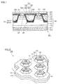
- a MOSFET 501 (silicon carbide semiconductor device) of the present embodiment includes an epitaxial substrate 100 (silicon carbide substrate), gate insulating films 201, gate electrodes 230, interlayer insulating films 203, source electrodes 221, a drain electrode 211, a source interconnection 222, and a protecting electrode 212.
- Epitaxial substrate 100 is made of silicon carbide, and has a single-crystal substrate 110 and an epitaxial layer provided thereon.
- Single-crystal substrate 110 has n type conductivity (first conductivity type).
- the plane orientation (hklm) of one main surface (upper surface in Fig. 1 ) of single-crystal substrate 110 preferably has m of negative value, more preferably, is approximately a (000-1) plane.
- the epitaxial layer of epitaxial substrate 100 includes an n - layer 121 (first semiconductor layer), p type body layers 122 (second semiconductor layer), n regions 123 (third semiconductor layer), and contact regions 124.
- the silicon carbide of epitaxial substrate 100 preferably has a hexagonal crystal structure, more preferably, has polytype of 4H.
- N - layer 121 has a donor added therein, and therefore has n type conductivity.
- the donor is preferably added to n - layer 121 by adding an impurity during epitaxial growth of n - layer 121, rather than ion implantation.
- N - layer 121 preferably has a donor concentration lower than that of single-crystal substrate 110.
- the donor concentration of n - layer 121 is preferably not less than 1 ⁇ 10 15 cm -3 and not more than 5 ⁇ 10 16 cm -3 , for example, 8 ⁇ 10 15 cm -3 .
- Each of p type body layers 122 is provided on n - layer 121, has an acceptor added therein, and therefore has p type conductivity (second conductivity type different from the first conductivity type).
- P type body layer 122 has an acceptor concentration of, for example, 1 ⁇ 10 18 cm -3 .
- N region 123 has n type conductivity.
- N region 123 is provided on p type body layer 122, and is separated from n - layer 121 by p type body layer 122.
- Each of contact regions 124 has p type conductivity. Contact region 124 is formed on a portion of p type body layer 122 so as to be connected to p type body layer 122.
- Trench TR includes: a bottom surface BT constituted of n - layer 121; and a side wall surface SW having side surfaces SW1 to SW3 (first to third side surfaces). Side surfaces SW1 to SW3 are respectively constituted of n - layer 121, p type body layer 122, and n region 123.
- Bottom surface BT is a flat surface substantially parallel to the main surface of epitaxial substrate 100.
- Trench TR has a corner portion CR formed by side surface SW1 and bottom surface BT meeting each other.
- Side surface SW2 has a function as a channel of the MOSFET.
- side wall surface SW in particular, side surface SW2 has a predetermined crystal plane (also referred to as "special plane"). Details of the special plane will be described later.
- epitaxial substrate 100 has trench TR corresponds to such a fact that the epitaxial layer is partially removed above the upper surface of single-crystal substrate 110.
- a multiplicity of mesa structures are formed on the upper surface of single-crystal substrate 110.
- each of the mesa structures has upper surface and bottom surface both having a hexagonal shape, and has side walls inclined relative to the upper surface of single-crystal substrate 110. Accordingly, trench TR is expanded toward the opening side.
- Gate insulating film 201 is provided on trench TR. Gate insulating film 201 separates epitaxial substrate 100 and gate electrode 230 from each other in trench TR. Gate insulating film 201 is preferably an oxide film, such as a silicon oxide film.
- Gate insulating film 201 includes: a bottom portion 201B covering bottom surface BT; and a side wall portion 201S connected to bottom portion 201B and covering side wall surface SW.
- Bottom portion 201B has a thickness d 0 .
- a portion of side wall portion 201S on side surface SW2 has a minimum thickness d 1 .
- a portion, connected to bottom portion 201B, of side wall portion 201S on side surface SW1 has a thickness d 2 .
- the portion having thickness d 1 and the portion having thickness d 2 are connected to each other at a boundary portion BP, which is a region in which a thickness is changed.
- boundary portion BP is located deeper (downward in the figure) than a boundary between side surfaces SW1 and SW2.
- d 2 > d 1 is satisfied.
- d 0 > d 1 is satisfied.
- side wall portion 201 S connects n - layer 121 and n region 123 to each other on side surface SW2 by a portion having a thickness less than thickness d 2 .
- side wall portion 201 S connects n - layer 121 and n region 123 to each other on side surface SW2 by the portion having thickness d 1 .
- Gate electrode 230 is provided on trench TR with gate insulating film 201 being interposed therebetween. Namely, gate electrode 230 faces each of side surfaces SW1 to SW3 and bottom surface BT with gate insulating film 201 being interposed therebetween.
- Source electrode 221 extends through interlayer insulating film 203 and is in contact with each of n region 123 and contact region 124.
- Source interconnection 222 is provided on source electrode 221 and interlayer insulating film 203 in contact with source electrode 221.
- Drain electrode 211 is provided on an opposite surface of epitaxial substrate 100 to its surface provided with trench TR.
- Protecting electrode 212 covers drain electrode 211.
- MOSFET 501 Fig. 1
- n - layer 121 is formed by means of epitaxial growth.
- This epitaxial growth can be achieved by employing a CVD (Chemical Vapor Deposition) method that utilizes a mixed gas of silane (SiH 4 ) and propane (C 3 H 8 ) as a material gas and utilizes hydrogen gas (H 2 ) as a carrier gas, for example. In doing so, it is preferable to introduce nitrogen (N) or phosphorus (P) as donors, for example.
- CVD Chemical Vapor Deposition
- p type body layer 122 is formed on n - layer 121, and n region 123 is formed on p type body layer 122.
- ions are implanted into the upper surface of n - layer 121.
- ions of an acceptor such as aluminum (Al) are implanted.
- ions of a donor such as phosphorus (P) are implanted, for example.
- epitaxial growth involving addition of an impurity may be employed.
- contact regions 124 are formed.
- an activation heating treatment is performed to activate the impurities added by the ion implantation.
- This heating treatment is preferably performed at a temperature of not less than 1500°C and not more than 1900°C, for example, a temperature of approximately 1700°C.
- the heating treatment is performed for approximately 30 minutes, for example.
- the atmosphere of the heating treatment is preferably an inert gas atmosphere, such as Ar atmosphere.
- epitaxial substrate 100 is prepared.
- a mask 401 having an opening partially exposing n region 123 is formed on epitaxial substrate 100.
- the opening is disposed in conformity with the position of trench TR ( Fig. 1 ).
- a silicon oxide film formed by thermal oxidation can be used, for example.
- etching in the opening of mask 401, n region 123, p type body layer 122, and portions of n - layer 121 are removed by etching.
- An exemplary, usable etching method is reactive ion etching (RIE), in particular, inductively coupled plasma (ICP) RIE Specifically, for example, ICP-RIE can be used which employs SF 6 or a mixed gas of SF 6 and O 2 as the reaction gas.
- RIE reactive ion etching
- ICP-RIE inductively coupled plasma
- a recess TQ can be formed which has a side wall having an inner surface SV substantially perpendicular to the main surface of single-crystal substrate 110.
- epitaxial substrate 100 is etched using mask 401. Specifically, inner surface SV of recess TQ of epitaxial substrate 100 is thermally etched.
- the thermal etching can be performed by, for example, heating epitaxial substrate 100 in an atmosphere containing a reactive gas having at least one or more types of halogen atom.
- the at least one or more types of halogen atom include at least one of chlorine (Cl) atom and fluorine (F) atom.
- This atmosphere is, for example, Cl 2 , BCL 3 , SF 6 , or CF 4 .
- the thermal etching is performed using a mixed gas of chlorine gas and oxygen gas as a reactive gas, at a heating treatment temperature of, for example, not less than 700°C and not more than 1000°C.
- the reactive gas may contain a carrier gas.
- An exemplary, usable carrier gas is nitrogen (N 2 ) gas, argon gas, helium gas, or the like.
- trench TR is formed in the epitaxial layer of silicon carbide substrate 100 by the above-mentioned thermal etching.
- epitaxial substrate 100 is side-etched from the opening of mask 401 as indicated by an arrow SE.
- a special plane is spontaneously formed on side wall surface SW of trench TR, in particular, on side surface SW2.
- mask 401 is removed by wet etching, for example ( Fig. 8 ).
- the wet etching can be performed using hydrofluoric acid, for example.
- thermal oxidation film 201P is formed on the trench by thermal oxidation of epitaxial substrate 100.
- the thermal oxidation may be performed at a temperature of less than 1300°C or not less than 1300°C.
- silicon film 302P is formed to fill trench TR with thermal oxidation film 201 interposed therebetween.
- Silicon film 302P can be formed by the chemical vapor deposition (CVD) method, for example.
- CVD chemical vapor deposition
- silicon film 302P is thermally oxidized.
- a covering insulating film 201Q ( Fig. 11 ) is formed to cover a region extending from opening OP to corner portion CR.
- Silicon film 302P is preferably thermally oxidized at less than 1300°C, in particular, is more preferably thermally oxidized at less than 1100°C.
- silicon film 302P is preferably thermally oxidized at more than 900°C, and is more preferably thermally oxidized at more than 1000°C.
- a resist layer 402 is formed by applying a resist liquid to fill trench TR with covering insulating film 201 Q being interposed therebetween.
- resist layer 402 is patterned such that resist layer 402 partially remains in trench TR. The etch back may be performed without using an etching mask. Resist layer 402 thus remaining covers corner portion CR with covering insulating film 201Q being interposed therebetween.
- covering insulating film 201Q is etched using resist layer 402 as a mask. This etching is preferably performed by wet etching. The wet etching can be performed using hydrofluoric acid, for example.
- corner insulating film 201R is formed to cover corner portion CR and expose the region extending from opening OP onto side surface SW2.
- Corner insulating film 201R covers corner portion CR, and at least partially expose side surface SW2.
- the whole of side surface SW2 is exposed and a portion of side surface SW1 in contact with side surface SW2 is also exposed.
- resist layer 402 ( Fig. 14 ) is removed.
- trench TR having corner insulating film 201R provided thereon is thermally oxidized.
- epitaxial substrate 100 is heated at not less than 1300°C. That is, the thermal oxidation is performed at not less than 1300°C. Specifically, it is preferable to perform the following steps for the thermal oxidation.
- epitaxial substrate 100 is heated from a temperature of less than 1300°C to a temperature of not less than 1300°C in a non-oxidizing atmosphere.
- epitaxial substrate 100 is heated from a temperature of less than 1000°C (for example, about a room temperature) to a temperature of not less than 1300°C in the non-oxidizing atmosphere.
- the non-oxidizing atmosphere is an Ar atmosphere, for example.
- the atmosphere surrounding epitaxial substrate 100 is changed from the non-oxidizing atmosphere to an oxidizing atmosphere. Accordingly, epitaxial substrate 100 is thermally oxidized.
- This change can be made by introducing oxygen gas into the atmosphere surrounding epitaxial substrate 100.
- the change can be made from Ar atmosphere to an atmosphere of mixture of Ar gas and O 2 (oxygen) gas.
- the atmosphere surrounding epitaxial substrate 100 is changed from the oxidizing atmosphere to a non-oxidizing atmosphere. For example, a change is made from the atmosphere of mixture of Ar gas and O 2 gas to an Ar atmosphere.
- epitaxial substrate 100 is cooled from the temperature of not less than 1300°C to a temperature of not more than 1000°C (for example, about a room temperature).
- gate insulating film 201 ( Fig. 17 ) is formed to cover the region extending from opening OP to corner portion CR.
- gate electrode 230 is formed on trench TR with gate insulating film 201 being interposed therebetween.
- a method for forming gate electrode 230 can be performed by, for example, forming a film of conductor or doped polysilicon and performing CMP (Chemical Mechanical Polishing).
- interlayer insulating film 203 is formed on gate electrode 230 and gate insulating film 201 so as to cover the exposed surface of gate electrode 230. Etching is performed to form an opening in interlayer insulating film 203 and gate insulating film 201. Through the opening, each of n region 123 and contact region 124 is exposed on the upper surface of the mesa structure. Next, on the upper surface of the mesa structure, source electrode 221 is formed in contact with each of n region 123 and contact region 124. Source interconnection 222, drain electrode 211, and protecting electrode 212 are formed. In this way, MOSFET 501 is obtained.
- gate insulating film 201 formed by thermally oxidizing trench TR provided with corner insulating film 201R ( Fig. 15 ) is made thick at corner portion CR of trench TR by a thickness corresponding to the thickness of corner insulating film 201 R. Therefore, corner portion CR does not need to be made thick by thermal oxidation. Thus, it is not necessary to actively cause a phenomenon in which the thermal oxidation rate differs depending on crystal orientation. Hence, there can be employed thermal oxidation ( Fig. 16 ) at not less than 1300°C at which such a phenomenon hardly takes place. By thus selecting the temperature of thermal oxidation, it is possible to suppress the phenomenon in which gate insulating film 201 becomes thin near opening OP of trench TR. Therefore, sufficient insulation reliability of the gate insulating film can be secured near opening OP.
- the insulating film on opening OP is formed only by performing thermal oxidation at less than 1300°C, the insulating film has a small thickness near opening OP as in a gate insulating film 201Z ( Fig. 19 ).
- the temperature of epitaxial substrate 100 is increased from a temperature of less than 1300°C to a temperature of not less than 1300°C in a non-oxidizing atmosphere, and then the atmosphere surrounding epitaxial substrate 100 is changed from the non-oxidizing atmosphere to an oxidizing atmosphere while maintaining the temperature of epitaxial substrate 100 at not less than 1300°C.
- the atmosphere surrounding epitaxial substrate 100 is changed from the oxidizing atmosphere to a non-oxidizing atmosphere while maintaining the temperature of epitaxial substrate 100 at not less than 1300°C, and then epitaxial substrate 100 is cooled from the temperature of not less than 1300°C to a temperature of not more than 1000°C while maintaining, as the non-oxidizing atmosphere, the atmosphere surrounding epitaxial substrate 100. Accordingly, the thermal oxidation can be more sufficiently performed at not less than 1300°C.
- oxygen gas is preferably introduced into the atmosphere surrounding epitaxial substrate 100. In this way, the change can be made readily from the non-oxidizing atmosphere to the oxidizing atmosphere.
- corner insulating film 201R ( Fig. 15 )
- covering insulating film 201Q is formed ( Fig. 11 ) to cover the region extending from opening OP to corner portion CR, and is patterned ( Fig. 12 to Fig. 14 ).
- corner insulating film 201R can be formed from the film covering the region extending from opening OP to corner portion CR.
- covering insulating film 201Q is etched using, as a mask, resist layer 402 ( Fig. 13 ) patterned by etch back. Accordingly, covering insulating film 201Q can be patterned readily.
- Covering insulating film 201Q is preferably etched by wet etching. Accordingly, the etching is performed by chemical etching rather than physical etching. Therefore, the etching does not provide physical damage to epitaxial substrate 100.
- covering insulating film 201Q when forming covering insulating film 201Q ( Fig. 11 ), silicon film 302P is formed on trench TR ( Fig. 9 ) and is thermally oxidized ( Fig. 10 ). Accordingly, covering insulating film 201Q can be formed from silicon film 302P. Moreover, because not only silicon film 302P but also thermal oxidation film 201P are formed, covering insulating film 201Q can be made thicker.
- Silicon film 302P is preferably thermally oxidized at less than 1300°C, in particular, is more preferably thermally oxidized at less than 1100°C. Accordingly, insulating property can be suppressed from being deteriorated due to generation of SiO by reaction between thermal oxidation film 201P and silicon film 302P. Moreover, in order to proceed the thermal oxidation at a practically sufficient rate, silicon film 302P is preferably thermally oxidized at more than 900°C. Moreover, in order to reduce stress stored in the thermal oxidation film, silicon film 302P is preferably thermally oxidized at more than 1000°C, which is a temperature with which the thermal oxidation film can be made soft.
- boundary portion BP is located on the boundary between side surfaces SW1 and SW2.
- the expression "located on the boundary” herein is intended to permit an error of, specifically, about ⁇ 0.1 ⁇ m, rather than permitting no production error at all.
- Boundary portion BP can be positioned in this way by, for example, suppressing a degree of advance of the etch back step ( Fig. 12 and Fig. 13 ) in the first embodiment.
- the configuration of the present embodiment is substantially the same as the configuration of the first embodiment. Hence, the same or corresponding elements are given the same reference characters and are not described repeatedly.
- side wall portion 201S of gate insulating film 201 connects between p type body layer 122 and bottom portion 201B on side surface SW1 by a portion having a thickness more than thickness d 1 . Accordingly, the portion of side wall portion 201 S on side surface SW1 has a thickness more than thickness d 1 in a wider range. Therefore, dielectric breakdown of gate insulating film 201 can be prevented more securely near corner portion CR of trench TR.
- Side wall portion 201 S of gate insulating film 201 may connect between p type body layer 122 and bottom portions 201B on side surface SW1 by a portion having thickness d 2 . Accordingly, the portion of side wall portion 201 S on side surface SW1 has a thickness d 2 more than thickness d 1 in a wider range. Therefore, the dielectric breakdown of gate insulating film 201 can be prevented more securely near corner portion CR of trench TR.
- side wall surface SW ( Fig. 3 ) of trench TR, in particular, side surface SW2 preferably has a predetermined crystal plane (also referred to as "special plane").
- a side wall surface SW includes a plane S1 (first plane) having a plane orientation of ⁇ 0-33-8 ⁇ as shown in Fig. 21 .
- Plane S1 preferably has a plane orientation of (0-33-8).
- side wall surface SW microscopically includes plane S1 and side wall surface SW microscopically further includes a plane S2 (second plane) having a plane orientation of ⁇ 0-11-1 ⁇ .
- plane S2 second plane
- plane orientation of ⁇ 0-11-1 ⁇ the term “microscopically” refers to "minutely to such an extent that at least the size about twice as large as an interatomic spacing is considered".
- a TEM Transmission Electron Microscope
- Plane S2 preferably has a plane orientation of (0-11-1).
- plane S1 and plane S2 of side wall surface SW constitutes a combined plane SR having a plane orientation of ⁇ 0-11-2 ⁇ .
- combined plane SR is formed of periodically repeated planes S1 and S2. Such a periodic structure can be observed by, for example, TEM or AFM (Atomic Force Microscopy).
- combined plane SR has an off angle of 62° relative to the ⁇ 000-1 ⁇ plane, macroscopically.
- the term "macroscopically” refers to "disregarding a fine structure having a size of approximately interatomic spacing".
- a method employing general X-ray diffraction can be used, for example.
- combined plane SR has a plane orientation of (0-11-2). In this case, combined plane SR has an off angle of 62° relative to the (000-1) plane, macroscopically.
- channels in which the above-described periodic repetition is done.
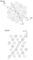
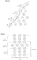
- Si atoms when viewing a silicon carbide single-crystal of polytype 4H from the (000-1) plane, atoms in a layer A (solid line in the figure), atoms in a layer B (broken line in the figure) disposed therebelow, and atoms in a layer C (chain line in the figure) disposed therebelow, and atoms in a layer B (not shown in the figure) disposed therebelow are repeatedly provided as shown in Fig. 22 .
- a periodic stacking structure such as ABCBABCBABCB ... is provided.
- combined surface SR is constructed by alternately providing planes S1 having a plane orientation of (0-33-8) and planes S2 connected to planes S1 and having a plane orientation different from that of each of planes S1.
- planes S1 and S2 has a length twice as large as the interatomic spacing of the Si atoms (or C atoms). It should be noted that a plane with plane S1 and plane S2 being averaged corresponds to the (0-11-2) plane ( Fig. 23 ).
- the single-crystal structure has a portion periodically including a structure (plane S1 portion) equivalent to a cubic structure.
- combined plane SR is constructed by alternately providing planes S1 having a plane orientation of (001) in the above-described structure equivalent to the cubic structure and planes S2 connected to planes S1 and having a plane orientation different from that of each of planes S1.
- the surface can be thus constituted of the planes (planes S1 in Fig. 25 ) having a plane orientation of (001) in the structure equivalent to the cubic structure and the planes (planes S2 in Fig. 25 ) connected to the foregoing planes and having a plane orientation different from that of each of the foregoing planes.
- the polytype may be 6H or 15R, for example.
- the horizontal axis represents an angle D1 formed by the (000-1) plane and the macroscopic plane orientation of side wall surface SW having the channel surface
- the vertical axis represents mobility MB.
- a group of plots CM correspond to a case where side wall surface SW is finished to correspond to a special plane by thermal etching
- a group of plots MC correspond to a case where side wall SW is not thermally etched.
- mobility MB is at maximum when the surface of the channel surface has a macroscopic plane orientation of (0-33-8). This is presumably due to the following reason. That is, in the case where the thermal etching is not performed, i.e., in the case where the microscopic structure of the channel surface is not particularly controlled, the macroscopic plane orientation thereof corresponds to (0-33-8), with the result that a ratio of the microscopic plane orientation of (0-33-8), i.e., the plane orientation of (0-33-8) in consideration of that in atomic level becomes statistically high.
- channel direction CD ( Fig. 21 ) preferably has an angle D2 of not less than 0° and not more than 60°, more preferably, substantially 0°.
- side wall surface SW may further include plane S3 (third plane) in addition to combined plane SR. More specifically, side wall surface SW may include a combined plane SQ constituted of periodically repeated plane S3 and combined plane SR.
- the off angle of side wall surface SW relative to the ⁇ 000-1 ⁇ plane is deviated from the ideal off angle of combined plane SR, i.e., 62°.
- this deviation is small, preferably, in a range of ⁇ 10°. Examples of a surface included in such an angle range include a surface having a macroscopic plane orientation of the ⁇ 0-33-8 ⁇ plane.
- the off angle of side wall surface SW relative to the (000-1) plane is deviated from the ideal off angle of combined plane SR, i.e., 62°.
- this deviation is small, preferably, in a range of ⁇ 10°.
- Examples of a surface included in such an angle range include a surface having a macroscopic plane orientation of the (0-33-8) plane.
- Such a periodic structure can be observed by TEM or AFM, for example.
- the silicon carbide semiconductor device may be a MISFET (Metal Insulator Semiconductor Field Effect Transistor) other than the MOSFET.
- the silicon carbide semiconductor device is not limited to the MISFET, and may be, for example, an IGBT (Insulated Gate Bipolar Transistor).
- the first and second conductivity types are not limited to the n type and the p type respectively but may be replaced with each other.
- 100 epitaxial substrate (silicon carbide substrate); 110: single-crystal substrate; 121: n - layer (first semiconductor layer); 122: p type body layer (second semiconductor layer); 123: n region (third semiconductor layer); 124: contact region; 201: gate insulating film; 201B: bottom portion; 201P: thermal oxidation film; 201Q: covering insulating film; 201 R: corner insulating film; 201S: side wall portion; 203: interlayer insulating film; 211: drain electrode; 212: protecting electrode; 221: source electrode; 222: source interconnection; 230: gate electrode; 302P: silicon film; 401: mask; 402: resist layer; 501, 502: MOSFET (silicon carbide semiconductor device); BP: boundary portion; BT: bottom surface; CR: corner portion; OP: opening; SW: side wall surface; SW1 to SW3: side surface (first to third side surfaces); TR: trench.
- MOSFET silicon carbide semiconductor device
Landscapes
- Chemical & Material Sciences (AREA)
- Chemical Kinetics & Catalysis (AREA)
- General Chemical & Material Sciences (AREA)
- Electrodes Of Semiconductors (AREA)
- Formation Of Insulating Films (AREA)
- Recrystallisation Techniques (AREA)
Abstract
Description
- The present invention relates to a method for manufacturing a silicon carbide semiconductor device, in particular, a method for manufacturing a silicon carbide semiconductor device having a trench.
- As a silicon carbide semiconductor device,
Japanese Patent Laying-Open No. 7-326755 - PTD 1:
Japanese Patent Laying-Open No. 7-326755 - In the technique described in the publication above, the thermal oxidation rate when forming the gate insulating film needs to have a sufficiently large crystal orientation dependence. In such a case, according to inspection by the present inventors, the thickness of the gate insulating film become thin locally at the opening of the trench. This results in low insulation reliability of the gate insulating film near the opening of the trench.
- The present invention has been made to solve the problem described above, and has an object to provide a method for manufacturing a silicon carbide semiconductor device capable of securing sufficient insulation reliability of a gate insulating film near an opening of a trench while preventing dielectric breakdown of the gate oxide film at a bottom portion of the trench.
- A method for manufacturing a silicon carbide semiconductor device in the present invention has the following steps.
- There is prepared a silicon carbide substrate including a first semiconductor layer, a second semiconductor layer, and a third semiconductor layer, the first semiconductor layer having a first conductivity type, the second semiconductor layer being provided on the first semiconductor layer, the second semiconductor layer having a second conductivity type, the third semiconductor layer being provided on the second semiconductor layer, the third semiconductor layer being separated from the first semiconductor layer by the second semiconductor layer, the third semiconductor layer having the first conductivity type.
- A trench having an opening in the silicon carbide substrate is formed. The trench includes a bottom surface and a side wall surface, the bottom surface being constituted of the first semiconductor layer, the side wall surface having first to third side surfaces respectively constituted of the first to third semiconductor layers. The trench has a corner portion formed by the first side surface and the bottom surface meeting each other.
- A corner insulating film is formed to cover the corner portion and expose a region extending from the opening onto the second side surface.
- A gate insulating film is formed to cover a region extending from the opening to the corner portion. The step of forming the gate insulating film includes a step of thermally oxidizing the trench provided with the corner insulating film. The step of thermally oxidizing the trench includes a step of heating the silicon carbide substrate at not less than 1300°C.
- A gate electrode is formed on the trench with the gate insulating film being interposed therebetween.
- According to the present invention, sufficient insulation reliability of the gate insulating film can be secured near the opening of the trench.
-
-
Fig. 1 is a partial cross sectional view schematically showing a configuration of a silicon carbide semiconductor device in a first embodiment of the present invention. -
Fig. 2 is a perspective view schematically showing the shape of a silicon carbide substrate included in the silicon carbide semiconductor device ofFig. 1 with hatching being provided to a region of second conductivity type for viewability of the figure. -
Fig. 3 is an enlarged view ofFig. 1 . -
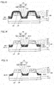
Fig. 4 is a partial cross sectional view schematically showing a first step of a method for manufacturing the silicon carbide semiconductor device ofFig. 1 . -
Fig. 5 is a partial cross sectional view schematically showing a second step of the method for manufacturing the silicon carbide semiconductor device ofFig. 1 . -
Fig. 6 is a partial cross sectional view schematically showing a third step of the method for manufacturing the silicon carbide semiconductor device ofFig. 1 . -
Fig. 7 is a partial cross sectional view schematically showing a fourth step of the method for manufacturing the silicon carbide semiconductor device ofFig. 1 . -
Fig. 8 is a partial cross sectional view schematically showing a fifth step of the method for manufacturing the silicon carbide semiconductor device ofFig. 1 . -
Fig. 9 is a partial cross sectional view schematically showing a sixth step of the method for manufacturing the silicon carbide semiconductor device ofFig. 1 . -
Fig. 10 is a partial cross sectional view schematically showing a seventh step of the method for manufacturing the silicon carbide semiconductor device ofFig. 1 . -
Fig. 11 is a partial cross sectional view schematically showing an eighth step of the method for manufacturing the silicon carbide semiconductor device ofFig. 1 . -
Fig. 12 is a partial cross sectional view schematically showing a ninth step of the method for manufacturing the silicon carbide semiconductor device ofFig. 1 . -
Fig. 13 is a partial cross sectional view schematically showing a tenth step of the method for manufacturing the silicon carbide semiconductor device ofFig. 1 . -
Fig. 14 is a partial cross sectional view schematically showing an eleventh step of the method for manufacturing the silicon carbide semiconductor device ofFig. 1 . -
Fig. 15 is a partial cross sectional view schematically showing a twelfth step of the method for manufacturing the silicon carbide semiconductor device ofFig. 1 . -
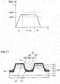
Fig. 16 is a graph showing an example of a process condition in a thirteenth step of the method for manufacturing the silicon carbide semiconductor device ofFig. 1 . -
Fig. 17 is a partial cross sectional view schematically showing the thirteenth step of the method for manufacturing the silicon carbide semiconductor device ofFig. 1 . -
Fig. 18 is a partial cross sectional view schematically showing a fourteenth step of the method for manufacturing the silicon carbide semiconductor device ofFig. 1 . -
Fig. 19 is a partial cross sectional view showing one step of a method for manufacturing a silicon carbide semiconductor device of a Comparative Example. -
Fig. 20 is a partial cross sectional view schematically showing a configuration of a silicon carbide semiconductor device in a second embodiment of the present invention. -
Fig. 21 is a partial cross sectional view schematically showing a fine structure in a surface of the silicon carbide substrate included in the silicon carbide semiconductor device. -
Fig. 22 shows a crystal structure of a (000-1) plane in a hexagonal crystal of polytype 4H. -
Fig. 23 shows a crystal structure of a (11-20) plane along a line XXIII-XXIII ofFig. 22 . -
Fig. 24 shows a crystal structure in the vicinity of a surface with a combined plane ofFig. 21 within a (11-20) plane. -
Fig. 25 shows the combined plane ofFig. 21 when viewed from a (01-10) plane. -
Fig. 26 is a graph showing an exemplary relation between channel mobility and an angle between a channel surface and the (000-1) plane when macroscopically viewed, in each of a case where thermal etching is performed and a case where no thermal etching is performed. -
Fig. 27 is a graph showing an exemplary relation between the channel mobility and an angle between a channel direction and a <0-11-2> direction. -
Fig. 28 shows a modification ofFig. 21 . - The following describes embodiments of the present invention with reference to figures. It should be noted that in the below-mentioned figures, the same or corresponding portions are given the same reference characters and are not described repeatedly. Regarding crystallographic indications in the present specification, an individual orientation is represented by [], a group orientation is represented by < >, and an individual plane is represented by (), and a group plane is represented by {}. In addition, a negative crystallographic index is normally expressed by putting "-" (bar) above a numeral, but is expressed by putting the negative sign before the numeral in the present specification.
- The following first describes an overview with regard to (i) to (x).
- (i) A method for manufacturing a silicon
carbide semiconductor device
There is prepared asilicon carbide substrate 100 including afirst semiconductor layer 121, asecond semiconductor layer 122, and athird semiconductor layer 123,first semiconductor layer 121 having a first conductivity type,second semiconductor layer 122 being provided onfirst semiconductor layer 121,second semiconductor layer 122 having a second conductivity type,third semiconductor layer 123 being provided onsecond semiconductor layer 122,third semiconductor layer 123 being separated fromfirst semiconductor layer 121 bysecond semiconductor layer 122,third semiconductor layer 123 having the first conductivity type.
A trench TR having an opening OP insilicon carbide substrate 100 is formed. Trench TR includes a bottom surface BT and a side wall surface SW, bottom surface BT being constituted offirst semiconductor layer 121, side wall surface SW having first to third side surfaces SW1 to SW3 respectively constituted of first tothird semiconductor layers 121 to 123. Trench TR has a corner portion CR formed by first side surface SW1 and bottom surface BT meeting each other.
Acorner insulating film 201 R is formed to cover corner portion CR and expose a region extending from opening OP onto second side surface SW2.
Agate insulating film 201 is formed to cover a region extending from opening OP to corner portion CR. The step of forminggate insulating film 201 includes a step of thermally oxidizing trench TR provided withcorner insulating film 201R. The step of thermally oxidizing trench TR includes a step of heatingsilicon carbide substrate 100 at not less than 1300°C.
Agate electrode 230 is formed on trench TR withgate insulating film 201 being interposed therebetween.
According to the manufacturing method,gate insulating film 201 formed by thermally oxidizing trench TR provided withcorner insulating film 201R is made thick at corner portion CR of trench TR by a thickness corresponding to the thickness ofcorner insulating film 201R. Therefore, corner portion CR does not need to be made thick by thermal oxidation. Thus, it is not necessary to actively cause a phenomenon in which the thermal oxidation rate differs depending on crystal orientation. Hence, there can be employed thermal oxidation at not less than 1300°C at which such a phenomenon hardly takes place. By thus selecting the temperature of thermal oxidation, it is possible to suppress the phenomenon in whichgate insulating film 201 becomes thin near opening OP of trench TR. Therefore, sufficient insulation reliability of the gate insulating film can be secured near opening OP. - (ii) In (i), the step of thermally oxidizing trench TR preferably includes the following steps.
A temperature ofsilicon carbide substrate 100 is increased from a temperature of less than 1300°C to a temperature of not less than 1300°C in a non-oxidizing atmosphere. An atmosphere surroundingsilicon carbide substrate 100 is changed from the non-oxidizing atmosphere to an oxidizing atmosphere while maintaining the temperature ofsilicon carbide substrate 100 at not less than 1300°C.
Accordingly, the thermal oxidation can be more sufficiently performed at not less than 1300°C. - (iii) In (ii), the step of thermally oxidizing trench TR preferably includes the following steps.
The atmosphere surroundingsilicon carbide substrate 100 is changed from the oxidizing atmosphere to the non-oxidizing atmosphere while maintaining the temperature ofsilicon carbide substrate 100 at not less than 1300°C.Silicon carbide substrate 100 is cooled from the temperature of not less than 1300°C to a temperature of not more than 1000°C while maintaining, as the non-oxidizing atmosphere, the atmosphere surroundingsilicon carbide substrate 100.
Accordingly, the thermal oxidation can be more securely performed at not less than 1300°C. - (iv) In (ii) or (iii), the step of changing the atmosphere surrounding
silicon carbide substrate 100 from the non-oxidizing atmosphere to the oxidizing atmosphere preferably includes a step of introducing oxygen gas into the atmosphere surroundingsilicon carbide substrate 100.
In this way, the change can be made readily from the non-oxidizing atmosphere to the oxidizing atmosphere. - (v) In any one of (i) to (iv), the step of forming
corner insulating film 201R preferably includes the following steps.
A covering insulatingfilm 201 Q is formed to cover the region extending from opening OP to corner portion CR. Covering insulatingfilm 201Q is patterned.
In this way,corner insulating film 201 R can be formed from the film covering the region extending from opening OP to corner portion CR. - (vi) In (v), the step of forming covering insulating
film 201Q preferably includes the following steps.
Asilicon film 302P is formed on trench TR.Silicon film 302P is thermally oxidized.
Accordingly, covering insulatingfilm 201 Q can be formed usingsilicon film 302P. - (vii) In (vi), the step of forming covering insulating
film 201Q preferably includes a step of forming athermal oxidation film 201P on trench TR before the step of formingsilicon film 302P.
Accordingly, the portion formed fromthermal oxidation film 201P can be included in covering insulatingfilm 201Q. Therefore, covering insulatingfilm 201Q can be made thicker. - (viii) In (vii), the step of thermally oxidizing
silicon film 302P is preferably performed at less than 1300°C.
Accordingly, insulating property can be suppressed from being deteriorated due to generation of SiO by reaction betweenthermal oxidation film 201P andsilicon film 302P. - (ix) In (v) to (viii), the step of patterning covering insulating
film 201Q preferably includes the following steps.
A resistlayer 402 is formed by applying a resist liquid to fill trench TR with covering insulatingfilm 201Q being interposed therebetween.
Resistlayer 402 is patterned by etching back resistlayer 402 such that resistlayer 402 partially remains on trench TR.
Covering insulatingfilm 201Q is etched using resistlayer 402 as a mask after patterning resistlayer 402.
Accordingly, covering insulatingfilm 201Q can be patterned readily. - (x) In (ix), the step of etching covering insulating
film 201Q is preferably performed by wet etching.
Accordingly, the etching is performed by chemical etching rather than physical etching. Therefore, the etching does not provide physical damage tosilicon carbide substrate 100.
Next, as more detailed description, the following describes first and second embodiments and supplementary matters thereof - As shown in
Fig. 1 , a MOSFET 501 (silicon carbide semiconductor device) of the present embodiment includes an epitaxial substrate 100 (silicon carbide substrate),gate insulating films 201,gate electrodes 230,interlayer insulating films 203,source electrodes 221, adrain electrode 211, asource interconnection 222, and a protectingelectrode 212. -
Epitaxial substrate 100 is made of silicon carbide, and has a single-crystal substrate 110 and an epitaxial layer provided thereon. Single-crystal substrate 110 has n type conductivity (first conductivity type). The plane orientation (hklm) of one main surface (upper surface inFig. 1 ) of single-crystal substrate 110 preferably has m of negative value, more preferably, is approximately a (000-1) plane. - Further, with reference to
Fig. 2 , the epitaxial layer ofepitaxial substrate 100 includes an n- layer 121 (first semiconductor layer), p type body layers 122 (second semiconductor layer), n regions 123 (third semiconductor layer), andcontact regions 124. The silicon carbide ofepitaxial substrate 100 preferably has a hexagonal crystal structure, more preferably, has polytype of 4H. - N- layer 121 has a donor added therein, and therefore has n type conductivity. The donor is preferably added to n- layer 121 by adding an impurity during epitaxial growth of n- layer 121, rather than ion implantation. N- layer 121 preferably has a donor concentration lower than that of single-
crystal substrate 110. The donor concentration of n- layer 121 is preferably not less than 1 × 1015 cm-3 and not more than 5 × 1016 cm-3, for example, 8 × 1015cm-3. - Each of p type body layers 122 is provided on n- layer 121, has an acceptor added therein, and therefore has p type conductivity (second conductivity type different from the first conductivity type). P
type body layer 122 has an acceptor concentration of, for example, 1 × 1018 cm-3. - Each of
n regions 123 has n type conductivity.N region 123 is provided on ptype body layer 122, and is separated from n- layer 121 by ptype body layer 122. - Each of
contact regions 124 has p type conductivity.Contact region 124 is formed on a portion of ptype body layer 122 so as to be connected to ptype body layer 122. - With reference to
Fig. 3 , a trench TR having an opening OP is provided in the epitaxial layer ofepitaxial substrate 100. Trench TR includes: a bottom surface BT constituted of n- layer 121; and a side wall surface SW having side surfaces SW1 to SW3 (first to third side surfaces). Side surfaces SW1 to SW3 are respectively constituted of n- layer 121, ptype body layer 122, andn region 123. - Bottom surface BT is a flat surface substantially parallel to the main surface of
epitaxial substrate 100. Trench TR has a corner portion CR formed by side surface SW1 and bottom surface BT meeting each other. Side surface SW2 has a function as a channel of the MOSFET. Preferably, side wall surface SW, in particular, side surface SW2 has a predetermined crystal plane (also referred to as "special plane"). Details of the special plane will be described later. - The fact that
epitaxial substrate 100 has trench TR corresponds to such a fact that the epitaxial layer is partially removed above the upper surface of single-crystal substrate 110. In the present embodiment, a multiplicity of mesa structures are formed on the upper surface of single-crystal substrate 110. Specifically, each of the mesa structures has upper surface and bottom surface both having a hexagonal shape, and has side walls inclined relative to the upper surface of single-crystal substrate 110. Accordingly, trench TR is expanded toward the opening side. -
Gate insulating film 201 is provided on trench TR.Gate insulating film 201 separatesepitaxial substrate 100 andgate electrode 230 from each other in trench TR.Gate insulating film 201 is preferably an oxide film, such as a silicon oxide film. -
Gate insulating film 201 includes: abottom portion 201B covering bottom surface BT; and aside wall portion 201S connected tobottom portion 201B and covering side wall surface SW.Bottom portion 201B has a thickness d0. A portion ofside wall portion 201S on side surface SW2 has a minimum thickness d1. A portion, connected tobottom portion 201B, ofside wall portion 201S on side surface SW1 has a thickness d2. In the present embodiment, the portion having thickness d1 and the portion having thickness d2 are connected to each other at a boundary portion BP, which is a region in which a thickness is changed. In the present embodiment, boundary portion BP is located deeper (downward in the figure) than a boundary between side surfaces SW1 and SW2. - Regarding the above-described thickness, d2 > d1 is satisfied. Preferably, d0 > d1 is satisfied. Preferably,
side wall portion 201 S connects n- layer 121 andn region 123 to each other on side surface SW2 by a portion having a thickness less than thickness d2. Preferably,side wall portion 201 S connects n- layer 121 andn region 123 to each other on side surface SW2 by the portion having thickness d1. -
Gate electrode 230 is provided on trench TR withgate insulating film 201 being interposed therebetween. Namely,gate electrode 230 faces each of side surfaces SW1 to SW3 and bottom surface BT withgate insulating film 201 being interposed therebetween. -
Source electrode 221 extends throughinterlayer insulating film 203 and is in contact with each ofn region 123 andcontact region 124.Source interconnection 222 is provided onsource electrode 221 and interlayer insulatingfilm 203 in contact withsource electrode 221.Drain electrode 211 is provided on an opposite surface ofepitaxial substrate 100 to its surface provided with trench TR. Protectingelectrode 212 coversdrain electrode 211. - The following describes a method for manufacturing MOSFET 501 (
Fig. 1 ). - With reference to
Fig. 4 , on single-crystal substrate 110, n- layer 121 is formed by means of epitaxial growth. This epitaxial growth can be achieved by employing a CVD (Chemical Vapor Deposition) method that utilizes a mixed gas of silane (SiH4) and propane (C3H8) as a material gas and utilizes hydrogen gas (H2) as a carrier gas, for example. In doing so, it is preferable to introduce nitrogen (N) or phosphorus (P) as donors, for example. - Next, p
type body layer 122 is formed on n- layer 121, andn region 123 is formed on ptype body layer 122. Specifically, ions are implanted into the upper surface of n- layer 121. In the ion implantation for forming ptype body layer 122, ions of an acceptor such as aluminum (Al) are implanted. Meanwhile, in the ion implantation for formingn region 123, ions of a donor such as phosphorus (P) are implanted, for example. It should be noted that instead of the ion implantation, epitaxial growth involving addition of an impurity may be employed. Next, by means of ion implantation,contact regions 124 are formed. - Next, an activation heating treatment is performed to activate the impurities added by the ion implantation. This heating treatment is preferably performed at a temperature of not less than 1500°C and not more than 1900°C, for example, a temperature of approximately 1700°C. The heating treatment is performed for approximately 30 minutes, for example. The atmosphere of the heating treatment is preferably an inert gas atmosphere, such as Ar atmosphere. In the manner described above,
epitaxial substrate 100 is prepared. - As shown in
Fig. 5 , amask 401 having an opening partially exposingn region 123 is formed onepitaxial substrate 100. The opening is disposed in conformity with the position of trench TR (Fig. 1 ). Asmask 401, a silicon oxide film formed by thermal oxidation can be used, for example. - As shown in
Fig. 6 , in the opening ofmask 401,n region 123, ptype body layer 122, and portions of n- layer 121 are removed by etching. An exemplary, usable etching method is reactive ion etching (RIE), in particular, inductively coupled plasma (ICP) RIE Specifically, for example, ICP-RIE can be used which employs SF6 or a mixed gas of SF6 and O2 as the reaction gas. By means of such etching, in the region where trench TR (Fig. 1 ) is to be formed, a recess TQ can be formed which has a side wall having an inner surface SV substantially perpendicular to the main surface of single-crystal substrate 110. - Next,
epitaxial substrate 100 is etched usingmask 401. Specifically, inner surface SV of recess TQ ofepitaxial substrate 100 is thermally etched. The thermal etching can be performed by, for example,heating epitaxial substrate 100 in an atmosphere containing a reactive gas having at least one or more types of halogen atom. The at least one or more types of halogen atom include at least one of chlorine (Cl) atom and fluorine (F) atom. This atmosphere is, for example, Cl2, BCL3, SF6, or CF4. For example, the thermal etching is performed using a mixed gas of chlorine gas and oxygen gas as a reactive gas, at a heating treatment temperature of, for example, not less than 700°C and not more than 1000°C. Further, the reactive gas may contain a carrier gas. An exemplary, usable carrier gas is nitrogen (N2) gas, argon gas, helium gas, or the like. When the heating treatment temperature is set at not less than 700°C and not more than 1000°C as described above, a rate of etching SiC is approximately, for example, 70 µm/hour. In addition, in this case,mask 401, which is formed of silicon oxide and therefore has a very large selection ratio relative to SiC, is not substantially etched during the etching of SiC. - As shown in
Fig. 7 , trench TR is formed in the epitaxial layer ofsilicon carbide substrate 100 by the above-mentioned thermal etching. During the formation of trench TR,epitaxial substrate 100 is side-etched from the opening ofmask 401 as indicated by an arrow SE. Further, during this thermal etching, a special plane is spontaneously formed on side wall surface SW of trench TR, in particular, on side surface SW2. Next,mask 401 is removed by wet etching, for example (Fig. 8 ). The wet etching can be performed using hydrofluoric acid, for example. - As shown in
Fig. 9 ,thermal oxidation film 201P is formed on the trench by thermal oxidation ofepitaxial substrate 100. The thermal oxidation may be performed at a temperature of less than 1300°C or not less than 1300°C. - As shown in
Fig. 10 ,silicon film 302P is formed to fill trench TR withthermal oxidation film 201 interposed therebetween.Silicon film 302P can be formed by the chemical vapor deposition (CVD) method, for example. Next,silicon film 302P is thermally oxidized. In this way, a covering insulatingfilm 201Q (Fig. 11 ) is formed to cover a region extending from opening OP to corner portion CR.Silicon film 302P is preferably thermally oxidized at less than 1300°C, in particular, is more preferably thermally oxidized at less than 1100°C. Moreover,silicon film 302P is preferably thermally oxidized at more than 900°C, and is more preferably thermally oxidized at more than 1000°C. - As shown in
Fig. 12 , a resistlayer 402 is formed by applying a resist liquid to fill trench TR with covering insulatingfilm 201 Q being interposed therebetween. As shown inFig. 13 , by etching back resistlayer 402, resistlayer 402 is patterned such that resistlayer 402 partially remains in trench TR. The etch back may be performed without using an etching mask. Resistlayer 402 thus remaining covers corner portion CR with covering insulatingfilm 201Q being interposed therebetween. After patterning resistlayer 402, covering insulatingfilm 201Q is etched using resistlayer 402 as a mask. This etching is preferably performed by wet etching. The wet etching can be performed using hydrofluoric acid, for example. - With the steps of
Fig. 12 andFig. 13 as described above, covering insulatingfilm 201Q is patterned. As a result, as shown inFig. 14 ,corner insulating film 201R is formed to cover corner portion CR and expose the region extending from opening OP onto side surface SW2. Corner insulatingfilm 201R covers corner portion CR, and at least partially expose side surface SW2. In the present embodiment, the whole of side surface SW2 is exposed and a portion of side surface SW1 in contact with side surface SW2 is also exposed. - As shown in
Fig. 15 , resist layer 402 (Fig. 14 ) is removed. Next, trench TR havingcorner insulating film 201R provided thereon is thermally oxidized. In the thermal oxidation,epitaxial substrate 100 is heated at not less than 1300°C. That is, the thermal oxidation is performed at not less than 1300°C. Specifically, it is preferable to perform the following steps for the thermal oxidation. - With reference to
Fig. 16 , first,epitaxial substrate 100 is heated from a temperature of less than 1300°C to a temperature of not less than 1300°C in a non-oxidizing atmosphere. Preferably,epitaxial substrate 100 is heated from a temperature of less than 1000°C (for example, about a room temperature) to a temperature of not less than 1300°C in the non-oxidizing atmosphere. The non-oxidizing atmosphere is an Ar atmosphere, for example. - Next, while maintaining the temperature of
epitaxial substrate 100 at not less than 1300°C, the atmosphere surroundingepitaxial substrate 100 is changed from the non-oxidizing atmosphere to an oxidizing atmosphere. Accordingly,epitaxial substrate 100 is thermally oxidized. This change can be made by introducing oxygen gas into the atmosphere surroundingepitaxial substrate 100. For example, the change can be made from Ar atmosphere to an atmosphere of mixture of Ar gas and O2 (oxygen) gas. - Next, while maintaining the temperature of
epitaxial substrate 100 at not less than 1300°C, the atmosphere surroundingepitaxial substrate 100 is changed from the oxidizing atmosphere to a non-oxidizing atmosphere. For example, a change is made from the atmosphere of mixture of Ar gas and O2 gas to an Ar atmosphere. Next, while maintaining, as the non-oxidizing atmosphere, the atmosphere surroundingepitaxial substrate 100,epitaxial substrate 100 is cooled from the temperature of not less than 1300°C to a temperature of not more than 1000°C (for example, about a room temperature). - In this way, gate insulating film 201 (
Fig. 17 ) is formed to cover the region extending from opening OP to corner portion CR. - As shown in
Fig. 18 ,gate electrode 230 is formed on trench TR withgate insulating film 201 being interposed therebetween. A method for forminggate electrode 230 can be performed by, for example, forming a film of conductor or doped polysilicon and performing CMP (Chemical Mechanical Polishing). - Referring to
Fig. 1 again, interlayer insulatingfilm 203 is formed ongate electrode 230 andgate insulating film 201 so as to cover the exposed surface ofgate electrode 230. Etching is performed to form an opening ininterlayer insulating film 203 andgate insulating film 201. Through the opening, each ofn region 123 andcontact region 124 is exposed on the upper surface of the mesa structure. Next, on the upper surface of the mesa structure,source electrode 221 is formed in contact with each ofn region 123 andcontact region 124.Source interconnection 222,drain electrode 211, and protectingelectrode 212 are formed. In this way,MOSFET 501 is obtained. - According to the present embodiment, gate insulating film 201 (
Fig. 16 ) formed by thermally oxidizing trench TR provided withcorner insulating film 201R (Fig. 15 ) is made thick at corner portion CR of trench TR by a thickness corresponding to the thickness ofcorner insulating film 201 R. Therefore, corner portion CR does not need to be made thick by thermal oxidation. Thus, it is not necessary to actively cause a phenomenon in which the thermal oxidation rate differs depending on crystal orientation. Hence, there can be employed thermal oxidation (Fig. 16 ) at not less than 1300°C at which such a phenomenon hardly takes place. By thus selecting the temperature of thermal oxidation, it is possible to suppress the phenomenon in whichgate insulating film 201 becomes thin near opening OP of trench TR. Therefore, sufficient insulation reliability of the gate insulating film can be secured near opening OP. - It should be noted that if the insulating film on opening OP is formed only by performing thermal oxidation at less than 1300°C, the insulating film has a small thickness near opening OP as in a
gate insulating film 201Z (Fig. 19 ). - Preferably, when trench TR provided with
corner insulating film 201R is thermally oxidized, the temperature ofepitaxial substrate 100 is increased from a temperature of less than 1300°C to a temperature of not less than 1300°C in a non-oxidizing atmosphere, and then the atmosphere surroundingepitaxial substrate 100 is changed from the non-oxidizing atmosphere to an oxidizing atmosphere while maintaining the temperature ofepitaxial substrate 100 at not less than 1300°C. More preferably, the atmosphere surroundingepitaxial substrate 100 is changed from the oxidizing atmosphere to a non-oxidizing atmosphere while maintaining the temperature ofepitaxial substrate 100 at not less than 1300°C, and thenepitaxial substrate 100 is cooled from the temperature of not less than 1300°C to a temperature of not more than 1000°C while maintaining, as the non-oxidizing atmosphere, the atmosphere surroundingepitaxial substrate 100. Accordingly, the thermal oxidation can be more sufficiently performed at not less than 1300°C. - When changing the atmosphere surrounding
epitaxial substrate 100 from the non-oxidizing atmosphere to the oxidizing atmosphere, oxygen gas is preferably introduced into the atmosphere surroundingepitaxial substrate 100. In this way, the change can be made readily from the non-oxidizing atmosphere to the oxidizing atmosphere. - Preferably, when forming
corner insulating film 201R (Fig. 15 ), covering insulatingfilm 201Q is formed (Fig. 11 ) to cover the region extending from opening OP to corner portion CR, and is patterned (Fig. 12 to Fig. 14 ). In this way,corner insulating film 201R can be formed from the film covering the region extending from opening OP to corner portion CR. - Preferably, when patterning covering insulating
film 201Q, covering insulatingfilm 201Q is etched using, as a mask, resist layer 402 (Fig. 13 ) patterned by etch back. Accordingly, covering insulatingfilm 201Q can be patterned readily. Covering insulatingfilm 201Q is preferably etched by wet etching. Accordingly, the etching is performed by chemical etching rather than physical etching. Therefore, the etching does not provide physical damage toepitaxial substrate 100. - Preferably, when forming covering insulating
film 201Q (Fig. 11 ),silicon film 302P is formed on trench TR (Fig. 9 ) and is thermally oxidized (Fig. 10 ). Accordingly, covering insulatingfilm 201Q can be formed fromsilicon film 302P. Moreover, because not onlysilicon film 302P but alsothermal oxidation film 201P are formed, covering insulatingfilm 201Q can be made thicker. -
Silicon film 302P is preferably thermally oxidized at less than 1300°C, in particular, is more preferably thermally oxidized at less than 1100°C. Accordingly, insulating property can be suppressed from being deteriorated due to generation of SiO by reaction betweenthermal oxidation film 201P andsilicon film 302P. Moreover, in order to proceed the thermal oxidation at a practically sufficient rate,silicon film 302P is preferably thermally oxidized at more than 900°C. Moreover, in order to reduce stress stored in the thermal oxidation film,silicon film 302P is preferably thermally oxidized at more than 1000°C, which is a temperature with which the thermal oxidation film can be made soft. - As shown in
Fig. 20 , in a MOSFET 502 (silicon carbide semiconductor device) of the present embodiment, unlike the first embodiment (Fig. 3 ), boundary portion BP is located on the boundary between side surfaces SW1 and SW2. The expression "located on the boundary" herein is intended to permit an error of, specifically, about ±0.1 µm, rather than permitting no production error at all. Boundary portion BP can be positioned in this way by, for example, suppressing a degree of advance of the etch back step (Fig. 12 andFig. 13 ) in the first embodiment. Apart from the configuration described above, the configuration of the present embodiment is substantially the same as the configuration of the first embodiment. Hence, the same or corresponding elements are given the same reference characters and are not described repeatedly. - By positioning boundary portion BP as described above,
side wall portion 201S ofgate insulating film 201 connects between ptype body layer 122 andbottom portion 201B on side surface SW1 by a portion having a thickness more than thickness d1. Accordingly, the portion ofside wall portion 201 S on side surface SW1 has a thickness more than thickness d1 in a wider range. Therefore, dielectric breakdown ofgate insulating film 201 can be prevented more securely near corner portion CR of trench TR. -
Side wall portion 201 S ofgate insulating film 201 may connect between ptype body layer 122 andbottom portions 201B on side surface SW1 by a portion having thickness d2. Accordingly, the portion ofside wall portion 201 S on side surface SW1 has a thickness d2 more than thickness d1 in a wider range. Therefore, the dielectric breakdown ofgate insulating film 201 can be prevented more securely near corner portion CR of trench TR. - As described above, side wall surface SW (
Fig. 3 ) of trench TR, in particular, side surface SW2 preferably has a predetermined crystal plane (also referred to as "special plane"). Such a side wall surface SW includes a plane S1 (first plane) having a plane orientation of {0-33-8} as shown inFig. 21 . Plane S1 preferably has a plane orientation of (0-33-8). - More preferably, side wall surface SW microscopically includes plane S1 and side wall surface SW microscopically further includes a plane S2 (second plane) having a plane orientation of {0-11-1}. Here, the term "microscopically" refers to "minutely to such an extent that at least the size about twice as large as an interatomic spacing is considered". As a method for observing such a microscopic structure, for example, a TEM (Transmission Electron Microscope) can be used. Plane S2 preferably has a plane orientation of (0-11-1).
- Preferably, plane S1 and plane S2 of side wall surface SW constitutes a combined plane SR having a plane orientation of {0-11-2}. Specifically, combined plane SR is formed of periodically repeated planes S1 and S2. Such a periodic structure can be observed by, for example, TEM or AFM (Atomic Force Microscopy). In this case, combined plane SR has an off angle of 62° relative to the {000-1} plane, macroscopically. Here, the term "macroscopically" refers to "disregarding a fine structure having a size of approximately interatomic spacing". For the measurement of such a macroscopic off angle, a method employing general X-ray diffraction can be used, for example. Preferably, combined plane SR has a plane orientation of (0-11-2). In this case, combined plane SR has an off angle of 62° relative to the (000-1) plane, macroscopically.
- Preferably, in the channel surface, carriers flow in a channel direction CD, in which the above-described periodic repetition is done.
- Next, a detailed structure of combined plane SR will be illustrated.
- Generally, regarding Si atoms (or C atoms), when viewing a silicon carbide single-crystal of polytype 4H from the (000-1) plane, atoms in a layer A (solid line in the figure), atoms in a layer B (broken line in the figure) disposed therebelow, and atoms in a layer C (chain line in the figure) disposed therebelow, and atoms in a layer B (not shown in the figure) disposed therebelow are repeatedly provided as shown in
Fig. 22 . In other words, with four layers ABCB being regarded as one period, a periodic stacking structure such as ABCBABCBABCB ... is provided. - As shown in
Fig. 23 , in the (11-20) plane (cross section taken along a line XXIII-XXIII ofFig. 22 ), atoms in each of four layers ABCB constituting the above-described one period are not aligned completely along the (0-11-2) plane. InFig. 23 , the (0-11-2) plane is illustrated to pass through the locations of the atoms in layers B. In this case, it is understood that each of atoms in layers A and C is deviated from the (0-11-2) plane. Hence, even when the macroscopic plane orientation of the surface of the silicon carbide single-crystal, i.e., the plane orientation thereof with its atomic level structure being ignored is limited to (0-11-2), this surface can have various structures microscopically. - As shown in
Fig. 24 , combined surface SR is constructed by alternately providing planes S1 having a plane orientation of (0-33-8) and planes S2 connected to planes S1 and having a plane orientation different from that of each of planes S1. Each of planes S1 and S2 has a length twice as large as the interatomic spacing of the Si atoms (or C atoms). It should be noted that a plane with plane S1 and plane S2 being averaged corresponds to the (0-11-2) plane (Fig. 23 ). - As shown in
Fig. 25 , when viewing combined plane SR from the (01-10) plane, the single-crystal structure has a portion periodically including a structure (plane S1 portion) equivalent to a cubic structure. Specifically, combined plane SR is constructed by alternately providing planes S1 having a plane orientation of (001) in the above-described structure equivalent to the cubic structure and planes S2 connected to planes S1 and having a plane orientation different from that of each of planes S1. Also in a polytype other than 4H, the surface can be thus constituted of the planes (planes S1 inFig. 25 ) having a plane orientation of (001) in the structure equivalent to the cubic structure and the planes (planes S2 inFig. 25 ) connected to the foregoing planes and having a plane orientation different from that of each of the foregoing planes. The polytype may be 6H or 15R, for example. - Next, with reference to
Fig. 26 , the following describes a relation between the crystal plane of side wall surface SW and mobility MB of the channel surface. In the graph ofFig. 26 , the horizontal axis represents an angle D1 formed by the (000-1) plane and the macroscopic plane orientation of side wall surface SW having the channel surface, whereas the vertical axis represents mobility MB. A group of plots CM correspond to a case where side wall surface SW is finished to correspond to a special plane by thermal etching, whereas a group of plots MC correspond to a case where side wall SW is not thermally etched. - In group of plots MC, mobility MB is at maximum when the surface of the channel surface has a macroscopic plane orientation of (0-33-8). This is presumably due to the following reason. That is, in the case where the thermal etching is not performed, i.e., in the case where the microscopic structure of the channel surface is not particularly controlled, the macroscopic plane orientation thereof corresponds to (0-33-8), with the result that a ratio of the microscopic plane orientation of (0-33-8), i.e., the plane orientation of (0-33-8) in consideration of that in atomic level becomes statistically high.
- On the other hand, mobility MB in group of plots CM is at maximum when the macroscopic plane orientation of the channel surface is (0-11-2) (arrow EX). This is presumably due to the following reason. That is, as shown in
Fig. 24 and Fig. 25 , the multiplicity of planes S1 each having a plane orientation of (0-33-8) are densely and regularly arranged with planes S2 interposed therebetween, whereby a ratio of the microscopic plane orientation of (0-33-8) becomes high in the channel surface. - It should be noted that mobility MB has orientation dependency on combined plane SR. In a graph shown in
Fig. 27 , the horizontal axis represents an angle D2 between the channel direction and the <0-11-2> direction, whereas the vertical axis represents mobility MB (in any unit) in the channel surface. A broken line is supplementarily provided therein for viewability of the graph. From this graph, it has been found that in order to increase channel mobility MB, channel direction CD (Fig. 21 ) preferably has an angle D2 of not less than 0° and not more than 60°, more preferably, substantially 0°. - As shown in
Fig. 28 , side wall surface SW may further include plane S3 (third plane) in addition to combined plane SR. More specifically, side wall surface SW may include a combined plane SQ constituted of periodically repeated plane S3 and combined plane SR. In this case, the off angle of side wall surface SW relative to the {000-1} plane is deviated from the ideal off angle of combined plane SR, i.e., 62°. Preferably, this deviation is small, preferably, in a range of ±10°. Examples of a surface included in such an angle range include a surface having a macroscopic plane orientation of the {0-33-8} plane. More preferably, the off angle of side wall surface SW relative to the (000-1) plane is deviated from the ideal off angle of combined plane SR, i.e., 62°. Preferably, this deviation is small, preferably, in a range of ±10°. Examples of a surface included in such an angle range include a surface having a macroscopic plane orientation of the (0-33-8) plane. - Such a periodic structure can be observed by TEM or AFM, for example.
- The embodiments disclosed herein are illustrative and non-restrictive in any respect. The scope of the present invention is defined by the terms of the claims, rather than the embodiments described above, and is intended to include any modifications within the scope and meaning equivalent to the terms of the claims. For example, the silicon carbide semiconductor device may be a MISFET (Metal Insulator Semiconductor Field Effect Transistor) other than the MOSFET. Further, the silicon carbide semiconductor device is not limited to the MISFET, and may be, for example, an IGBT (Insulated Gate Bipolar Transistor). Moreover, the first and second conductivity types are not limited to the n type and the p type respectively but may be replaced with each other.
- 100: epitaxial substrate (silicon carbide substrate); 110: single-crystal substrate; 121: n- layer (first semiconductor layer); 122: p type body layer (second semiconductor layer); 123: n region (third semiconductor layer); 124: contact region; 201: gate insulating film; 201B: bottom portion; 201P: thermal oxidation film; 201Q: covering insulating film; 201 R: corner insulating film; 201S: side wall portion; 203: interlayer insulating film; 211: drain electrode; 212: protecting electrode; 221: source electrode; 222: source interconnection; 230: gate electrode; 302P: silicon film; 401: mask; 402: resist layer; 501, 502: MOSFET (silicon carbide semiconductor device); BP: boundary portion; BT: bottom surface; CR: corner portion; OP: opening; SW: side wall surface; SW1 to SW3: side surface (first to third side surfaces); TR: trench.
Claims (10)
- A method for manufacturing a silicon carbide semiconductor device comprising steps of:preparing a silicon carbide substrate including a first semiconductor layer, a second semiconductor layer, and a third semiconductor layer, said first semiconductor layer having a first conductivity type, said second semiconductor layer being provided on said first semiconductor layer, said second semiconductor layer having a second conductivity type, said third semiconductor layer being provided on said second semiconductor layer, said third semiconductor layer being separated from said first semiconductor layer by said second semiconductor layer, said third semiconductor layer having said first conductivity type; andforming a trench having an opening in said silicon carbide substrate, said trench including a bottom surface and a side wall surface, said bottom surface being constituted of said first semiconductor layer, said side wall surface having first to third side surfaces respectively constituted of said first to third semiconductor layers, said trench having a corner portion formed by said first side surface and said bottom surface meeting each other; andforming a corner insulating film to cover said corner portion and expose a region extending from said opening onto said second side surface;forming a gate insulating film to cover a region extending from said opening to said corner portion, the step of forming said gate insulating film including a step of thermally oxidizing said trench provided with said corner insulating film, the step of thermally oxidizing said trench including a step of heating said silicon carbide substrate at not less than 1300°C; andforming a gate electrode on said trench with said gate insulating film being interposed therebetween.
- The method for manufacturing the silicon carbide semiconductor device according to claim 1, wherein
the step of thermally oxidizing said trench includes steps of:increasing a temperature of said silicon carbide substrate from a temperature of less than 1300°C to a temperature of not less than 1300°C in a non-oxidizing atmosphere; andchanging an atmosphere surrounding said silicon carbide substrate from the non-oxidizing atmosphere to an oxidizing atmosphere while maintaining the temperature of said silicon carbide substrate at not less than 1300°C. - The method for manufacturing the silicon carbide semiconductor device according to claim 2, wherein
the step of thermally oxidizing said trench includes steps of:changing the atmosphere surrounding said silicon carbide substrate from the oxidizing atmosphere to the non-oxidizing atmosphere while maintaining the temperature of said silicon carbide substrate at not less than 1300°C; andcooling said silicon carbide substrate from the temperature of not less than 1300°C to a temperature of not more than 1000°C while maintaining, as the non-oxidizing atmosphere, the atmosphere surrounding said silicon carbide substrate. - The method for manufacturing the silicon carbide semiconductor device according to claim 2 or 3, wherein the step of changing the atmosphere surrounding said silicon carbide substrate from the non-oxidizing atmosphere to the oxidizing atmosphere includes a step of introducing oxygen gas into the atmosphere surrounding said silicon carbide substrate.
- The method for manufacturing the silicon carbide semiconductor device according to any one of claims 1 to 4, wherein
the step of forming said corner insulating film includes steps of:forming a covering insulating film to cover the region extending from said opening to said corner portion; andpatterning said covering insulating film. - The method for manufacturing the silicon carbide semiconductor device according to claim 5, wherein
the step of forming said covering insulating film includes steps of:forming a silicon film on said trench; andthermally oxidizing said silicon film. - The method for manufacturing the silicon carbide semiconductor device according to claim 6, wherein the step of forming said covering insulating film includes a step of forming a thermal oxidation film on said trench before the step of forming said silicon film.
- The method for manufacturing the silicon carbide semiconductor device according to claim 7, wherein the step of thermally oxidizing said silicon film is performed at less than 1300°C.
- The method for manufacturing the silicon carbide semiconductor device according to any one of claims 5 to 8, wherein
the step of patterning said covering insulating film includes steps of:forming a resist layer by applying a resist liquid to fill said trench with said covering insulating film being interposed therebetween;patterning said resist layer by etching back said resist layer such that said resist layer partially remains on said trench; andetching said covering insulating film using said resist layer as a mask after the step of patterning said resist layer. - The method for manufacturing the silicon carbide semiconductor device according to claim 9, wherein the step of etching said covering insulating film is performed by wet etching.
Applications Claiming Priority (2)
| Application Number | Priority Date | Filing Date | Title |
|---|---|---|---|
| JP2013085528A JP2014207403A (en) | 2013-04-16 | 2013-04-16 | Silicon carbide semiconductor device manufacturing method |
| PCT/JP2014/055566 WO2014171211A1 (en) | 2013-04-16 | 2014-03-05 | Method for manufacturing silicon carbide semiconductor device |
Publications (2)
| Publication Number | Publication Date |
|---|---|
| EP2988323A1 true EP2988323A1 (en) | 2016-02-24 |
| EP2988323A4 EP2988323A4 (en) | 2016-11-30 |
Family
ID=51731170
Family Applications (1)
| Application Number | Title | Priority Date | Filing Date |
|---|---|---|---|
| EP14784819.6A Withdrawn EP2988323A4 (en) | 2013-04-16 | 2014-03-05 | METHOD FOR MANUFACTURING SILICON CARBIDE SEMICONDUCTOR DEVICE |
Country Status (4)
| Country | Link |
|---|---|
| US (1) | US9793365B2 (en) |
| EP (1) | EP2988323A4 (en) |
| JP (1) | JP2014207403A (en) |
| WO (1) | WO2014171211A1 (en) |
Families Citing this family (2)
| Publication number | Priority date | Publication date | Assignee | Title |
|---|---|---|---|---|
| JP6131689B2 (en) * | 2013-04-16 | 2017-05-24 | 住友電気工業株式会社 | Method for manufacturing silicon carbide semiconductor device |
| CN111489962B (en) * | 2020-04-17 | 2023-09-26 | 重庆伟特森电子科技有限公司 | A method for preparing thick-bottomed trenches |
Family Cites Families (27)
| Publication number | Priority date | Publication date | Assignee | Title |
|---|---|---|---|---|
| JP2858411B2 (en) | 1994-03-30 | 1999-02-17 | 株式会社デンソー | Method for manufacturing semiconductor device |
| JP3471473B2 (en) | 1994-04-06 | 2003-12-02 | 株式会社デンソー | Semiconductor device and manufacturing method thereof |
| EP0676814B1 (en) * | 1994-04-06 | 2006-03-22 | Denso Corporation | Process of producing trench semiconductor device |
| JP3143670B2 (en) * | 1997-08-13 | 2001-03-07 | 工業技術院長 | Oxide thin film forming method |
| US6291298B1 (en) * | 1999-05-25 | 2001-09-18 | Advanced Analogic Technologies, Inc. | Process of manufacturing Trench gate semiconductor device having gate oxide layer with multiple thicknesses |
| JP4073176B2 (en) | 2001-04-02 | 2008-04-09 | 新電元工業株式会社 | Semiconductor device and manufacturing method thereof |
| US6674124B2 (en) | 2001-11-15 | 2004-01-06 | General Semiconductor, Inc. | Trench MOSFET having low gate charge |
| JP3713498B2 (en) | 2003-03-28 | 2005-11-09 | 株式会社東芝 | Semiconductor device and manufacturing method thereof |
| JP2005019668A (en) | 2003-06-26 | 2005-01-20 | Shindengen Electric Mfg Co Ltd | Semiconductor device |
| US7371641B2 (en) | 2004-10-29 | 2008-05-13 | International Rectifier Corporation | Method of making a trench MOSFET with deposited oxide |
| JP4956904B2 (en) * | 2005-03-25 | 2012-06-20 | 富士電機株式会社 | Silicon carbide semiconductor device and manufacturing method thereof |
| JP2006344760A (en) * | 2005-06-08 | 2006-12-21 | Sharp Corp | Trench-type MOSFET and manufacturing method thereof |
| JP2007096263A (en) * | 2005-08-31 | 2007-04-12 | Denso Corp | Silicon carbide semiconductor device and manufacturing method thereof. |
| JP4857698B2 (en) | 2005-10-05 | 2012-01-18 | トヨタ自動車株式会社 | Silicon carbide semiconductor device |
| US20100221917A1 (en) | 2006-01-30 | 2010-09-02 | Sumitomo Electric Industries, Ltd. | Method of manufacturing silicon carbide semiconductor device |
| JP2009088188A (en) | 2007-09-28 | 2009-04-23 | Sanyo Electric Co Ltd | Trench gate type transistor and manufacturing method thereof |
| JP2010147405A (en) * | 2008-12-22 | 2010-07-01 | Renesas Technology Corp | Semiconductor device and method of manufacturing the same |
| JP4911263B2 (en) | 2009-03-11 | 2012-04-04 | 三菱電機株式会社 | Method for manufacturing silicon carbide semiconductor device |
| US8252647B2 (en) | 2009-08-31 | 2012-08-28 | Alpha & Omega Semiconductor Incorporated | Fabrication of trench DMOS device having thick bottom shielding oxide |
| JP2011216651A (en) | 2010-03-31 | 2011-10-27 | Renesas Electronics Corp | Method of manufacturing semiconductor device |
| JP2012038771A (en) * | 2010-08-03 | 2012-02-23 | Sumitomo Electric Ind Ltd | Semiconductor device and manufacturing method thereof |
| US20120037983A1 (en) | 2010-08-10 | 2012-02-16 | Force Mos Technology Co., Ltd. | Trench mosfet with integrated schottky rectifier in same cell |
| WO2012098861A1 (en) | 2011-01-17 | 2012-07-26 | パナソニック株式会社 | Semiconductor device and method for manufacturing same |
| JP5395309B2 (en) * | 2011-03-23 | 2014-01-22 | パナソニック株式会社 | Semiconductor device and manufacturing method thereof |
| JP5637916B2 (en) * | 2011-03-31 | 2014-12-10 | トヨタ自動車株式会社 | Semiconductor device and manufacturing method thereof |
| US9024357B2 (en) * | 2011-04-15 | 2015-05-05 | Stmicroelectronics S.R.L. | Method for manufacturing a HEMT transistor and corresponding HEMT transistor |
| JP5759293B2 (en) | 2011-07-20 | 2015-08-05 | 住友電気工業株式会社 | Manufacturing method of semiconductor device |
-
2013
- 2013-04-16 JP JP2013085528A patent/JP2014207403A/en active Pending
-
2014
- 2014-03-05 WO PCT/JP2014/055566 patent/WO2014171211A1/en not_active Ceased
- 2014-03-05 US US14/784,272 patent/US9793365B2/en active Active
- 2014-03-05 EP EP14784819.6A patent/EP2988323A4/en not_active Withdrawn
Also Published As
| Publication number | Publication date |
|---|---|
| EP2988323A4 (en) | 2016-11-30 |
| WO2014171211A1 (en) | 2014-10-23 |
| US9793365B2 (en) | 2017-10-17 |
| JP2014207403A (en) | 2014-10-30 |
| US20160049485A1 (en) | 2016-02-18 |
Similar Documents
| Publication | Publication Date | Title |
|---|---|---|
| US9627487B2 (en) | Method for manufacturing silicon carbide semiconductor device and silicon carbide semiconductor device | |
| US9984879B2 (en) | Silicon carbide semiconductor device and method for manufacturing same | |
| US10014376B2 (en) | Silicon carbide semiconductor device having a trench with side walls and method for manufacturing same | |
| US10192967B2 (en) | Silicon carbide semiconductor with trench gate | |
| US20160126347A1 (en) | Silicon carbide semiconductor device | |
| US9543412B2 (en) | Method for manufacturing silicon carbide semiconductor device | |
| JP2013062392A (en) | Silicon carbide semiconductor device and manufacturing method of the same | |
| US8927368B2 (en) | Method for manufacturing silicon carbide semiconductor device | |
| US8772113B2 (en) | Method for manufacturing silicon carbide semiconductor device | |
| EP2851957B1 (en) | Silicon carbide semiconductor device | |
| US9793365B2 (en) | Method for manufacturing silicon carbide semiconductor device having trench | |
| EP2866265A1 (en) | Method of manufacturing silicon carbide semiconductor device and silicon carbide semiconductor device | |
| US9679986B2 (en) | Silicon carbide semiconductor device | |
| US20130306987A1 (en) | Silicon carbide semiconductor device and method for manufacturing same |
Legal Events
| Date | Code | Title | Description |
|---|---|---|---|
| PUAI | Public reference made under article 153(3) epc to a published international application that has entered the european phase |
Free format text: ORIGINAL CODE: 0009012 |
|
| 17P | Request for examination filed |
Effective date: 20150923 |
|
| AK | Designated contracting states |
Kind code of ref document: A1 Designated state(s): AL AT BE BG CH CY CZ DE DK EE ES FI FR GB GR HR HU IE IS IT LI LT LU LV MC MK MT NL NO PL PT RO RS SE SI SK SM TR |
|
| AX | Request for extension of the european patent |
Extension state: BA ME |
|
| RIN1 | Information on inventor provided before grant (corrected) |
Inventor name: MASUDA, TAKEYOSHI Inventor name: HIRATSUKA, KENJI Inventor name: SAITOH, YU |
|
| DAX | Request for extension of the european patent (deleted) | ||
| A4 | Supplementary search report drawn up and despatched |
Effective date: 20161031 |
|
| RIC1 | Information provided on ipc code assigned before grant |
Ipc: H01L 21/336 20060101AFI20161025BHEP Ipc: H01L 29/78 20060101ALI20161025BHEP |
|
| STAA | Information on the status of an ep patent application or granted ep patent |
Free format text: STATUS: THE APPLICATION HAS BEEN WITHDRAWN |
|
| 18W | Application withdrawn |
Effective date: 20170818 |