EP2985328A1 - Protective tape and semiconductor device manufacturing method using same - Google Patents
Protective tape and semiconductor device manufacturing method using same Download PDFInfo
- Publication number
- EP2985328A1 EP2985328A1 EP14890441.0A EP14890441A EP2985328A1 EP 2985328 A1 EP2985328 A1 EP 2985328A1 EP 14890441 A EP14890441 A EP 14890441A EP 2985328 A1 EP2985328 A1 EP 2985328A1
- Authority
- EP
- European Patent Office
- Prior art keywords
- protective tape
- adhesive layer
- thermoplastic resin
- layer
- adhesive
- Prior art date
- Legal status (The legal status is an assumption and is not a legal conclusion. Google has not performed a legal analysis and makes no representation as to the accuracy of the status listed.)
- Granted
Links
Images



Classifications
-
- H—ELECTRICITY
- H10—SEMICONDUCTOR DEVICES; ELECTRIC SOLID-STATE DEVICES NOT OTHERWISE PROVIDED FOR
- H10P—GENERIC PROCESSES OR APPARATUS FOR THE MANUFACTURE OR TREATMENT OF DEVICES COVERED BY CLASS H10
- H10P72/00—Handling or holding of wafers, substrates or devices during manufacture or treatment thereof
- H10P72/70—Handling or holding of wafers, substrates or devices during manufacture or treatment thereof for supporting or gripping
- H10P72/74—Handling or holding of wafers, substrates or devices during manufacture or treatment thereof for supporting or gripping using temporarily an auxiliary support
- H10P72/7402—Wafer tapes, e.g. grinding or dicing support tapes
-
- B—PERFORMING OPERATIONS; TRANSPORTING
- B32—LAYERED PRODUCTS
- B32B—LAYERED PRODUCTS, i.e. PRODUCTS BUILT-UP OF STRATA OF FLAT OR NON-FLAT, e.g. CELLULAR OR HONEYCOMB, FORM
- B32B27/00—Layered products comprising a layer of synthetic resin
-
- C—CHEMISTRY; METALLURGY
- C09—DYES; PAINTS; POLISHES; NATURAL RESINS; ADHESIVES; COMPOSITIONS NOT OTHERWISE PROVIDED FOR; APPLICATIONS OF MATERIALS NOT OTHERWISE PROVIDED FOR
- C09J—ADHESIVES; NON-MECHANICAL ASPECTS OF ADHESIVE PROCESSES IN GENERAL; ADHESIVE PROCESSES NOT PROVIDED FOR ELSEWHERE; USE OF MATERIALS AS ADHESIVES
- C09J7/00—Adhesives in the form of films or foils
- C09J7/20—Adhesives in the form of films or foils characterised by their carriers
- C09J7/29—Laminated material
-
- H—ELECTRICITY
- H10—SEMICONDUCTOR DEVICES; ELECTRIC SOLID-STATE DEVICES NOT OTHERWISE PROVIDED FOR
- H10P—GENERIC PROCESSES OR APPARATUS FOR THE MANUFACTURE OR TREATMENT OF DEVICES COVERED BY CLASS H10
- H10P52/00—Grinding, lapping or polishing of wafers, substrates or parts of devices
-
- H—ELECTRICITY
- H10—SEMICONDUCTOR DEVICES; ELECTRIC SOLID-STATE DEVICES NOT OTHERWISE PROVIDED FOR
- H10P—GENERIC PROCESSES OR APPARATUS FOR THE MANUFACTURE OR TREATMENT OF DEVICES COVERED BY CLASS H10
- H10P54/00—Cutting or separating of wafers, substrates or parts of devices
-
- H—ELECTRICITY
- H10—SEMICONDUCTOR DEVICES; ELECTRIC SOLID-STATE DEVICES NOT OTHERWISE PROVIDED FOR
- H10P—GENERIC PROCESSES OR APPARATUS FOR THE MANUFACTURE OR TREATMENT OF DEVICES COVERED BY CLASS H10
- H10P72/00—Handling or holding of wafers, substrates or devices during manufacture or treatment thereof
- H10P72/70—Handling or holding of wafers, substrates or devices during manufacture or treatment thereof for supporting or gripping
- H10P72/74—Handling or holding of wafers, substrates or devices during manufacture or treatment thereof for supporting or gripping using temporarily an auxiliary support
- H10P72/7412—Handling or holding of wafers, substrates or devices during manufacture or treatment thereof for supporting or gripping using temporarily an auxiliary support the auxiliary support including means facilitating the separation of a device or wafer from the auxiliary support
-
- H—ELECTRICITY
- H10—SEMICONDUCTOR DEVICES; ELECTRIC SOLID-STATE DEVICES NOT OTHERWISE PROVIDED FOR
- H10P—GENERIC PROCESSES OR APPARATUS FOR THE MANUFACTURE OR TREATMENT OF DEVICES COVERED BY CLASS H10
- H10P72/00—Handling or holding of wafers, substrates or devices during manufacture or treatment thereof
- H10P72/70—Handling or holding of wafers, substrates or devices during manufacture or treatment thereof for supporting or gripping
- H10P72/74—Handling or holding of wafers, substrates or devices during manufacture or treatment thereof for supporting or gripping using temporarily an auxiliary support
- H10P72/7416—Handling or holding of wafers, substrates or devices during manufacture or treatment thereof for supporting or gripping using temporarily an auxiliary support used during dicing or grinding
-
- H—ELECTRICITY
- H10—SEMICONDUCTOR DEVICES; ELECTRIC SOLID-STATE DEVICES NOT OTHERWISE PROVIDED FOR
- H10P—GENERIC PROCESSES OR APPARATUS FOR THE MANUFACTURE OR TREATMENT OF DEVICES COVERED BY CLASS H10
- H10P72/00—Handling or holding of wafers, substrates or devices during manufacture or treatment thereof
- H10P72/70—Handling or holding of wafers, substrates or devices during manufacture or treatment thereof for supporting or gripping
- H10P72/74—Handling or holding of wafers, substrates or devices during manufacture or treatment thereof for supporting or gripping using temporarily an auxiliary support
- H10P72/7422—Handling or holding of wafers, substrates or devices during manufacture or treatment thereof for supporting or gripping using temporarily an auxiliary support used to protect an active side of a device or wafer
-
- H—ELECTRICITY
- H10—SEMICONDUCTOR DEVICES; ELECTRIC SOLID-STATE DEVICES NOT OTHERWISE PROVIDED FOR
- H10W—GENERIC PACKAGES, INTERCONNECTIONS, CONNECTORS OR OTHER CONSTRUCTIONAL DETAILS OF DEVICES COVERED BY CLASS H10
- H10W74/00—Encapsulations, e.g. protective coatings
- H10W74/10—Encapsulations, e.g. protective coatings characterised by their shape or disposition
- H10W74/111—Encapsulations, e.g. protective coatings characterised by their shape or disposition the semiconductor body being completely enclosed
- H10W74/127—Encapsulations, e.g. protective coatings characterised by their shape or disposition the semiconductor body being completely enclosed characterised by arrangements for sealing or adhesion
-
- B—PERFORMING OPERATIONS; TRANSPORTING
- B32—LAYERED PRODUCTS
- B32B—LAYERED PRODUCTS, i.e. PRODUCTS BUILT-UP OF STRATA OF FLAT OR NON-FLAT, e.g. CELLULAR OR HONEYCOMB, FORM
- B32B27/00—Layered products comprising a layer of synthetic resin
- B32B27/06—Layered products comprising a layer of synthetic resin as the main or only constituent of a layer, which is next to another layer of the same or of a different material
-
- C—CHEMISTRY; METALLURGY
- C09—DYES; PAINTS; POLISHES; NATURAL RESINS; ADHESIVES; COMPOSITIONS NOT OTHERWISE PROVIDED FOR; APPLICATIONS OF MATERIALS NOT OTHERWISE PROVIDED FOR
- C09J—ADHESIVES; NON-MECHANICAL ASPECTS OF ADHESIVE PROCESSES IN GENERAL; ADHESIVE PROCESSES NOT PROVIDED FOR ELSEWHERE; USE OF MATERIALS AS ADHESIVES
- C09J2203/00—Applications of adhesives in processes or use of adhesives in the form of films or foils
- C09J2203/326—Applications of adhesives in processes or use of adhesives in the form of films or foils for bonding electronic components such as wafers, chips or semiconductors
-
- C—CHEMISTRY; METALLURGY
- C09—DYES; PAINTS; POLISHES; NATURAL RESINS; ADHESIVES; COMPOSITIONS NOT OTHERWISE PROVIDED FOR; APPLICATIONS OF MATERIALS NOT OTHERWISE PROVIDED FOR
- C09J—ADHESIVES; NON-MECHANICAL ASPECTS OF ADHESIVE PROCESSES IN GENERAL; ADHESIVE PROCESSES NOT PROVIDED FOR ELSEWHERE; USE OF MATERIALS AS ADHESIVES
- C09J2301/00—Additional features of adhesives in the form of films or foils
- C09J2301/10—Additional features of adhesives in the form of films or foils characterized by the structural features of the adhesive tape or sheet
- C09J2301/12—Additional features of adhesives in the form of films or foils characterized by the structural features of the adhesive tape or sheet by the arrangement of layers
- C09J2301/122—Additional features of adhesives in the form of films or foils characterized by the structural features of the adhesive tape or sheet by the arrangement of layers the adhesive layer being present only on one side of the carrier, e.g. single-sided adhesive tape
-
- C—CHEMISTRY; METALLURGY
- C09—DYES; PAINTS; POLISHES; NATURAL RESINS; ADHESIVES; COMPOSITIONS NOT OTHERWISE PROVIDED FOR; APPLICATIONS OF MATERIALS NOT OTHERWISE PROVIDED FOR
- C09J—ADHESIVES; NON-MECHANICAL ASPECTS OF ADHESIVE PROCESSES IN GENERAL; ADHESIVE PROCESSES NOT PROVIDED FOR ELSEWHERE; USE OF MATERIALS AS ADHESIVES
- C09J2301/00—Additional features of adhesives in the form of films or foils
- C09J2301/30—Additional features of adhesives in the form of films or foils characterized by the chemical, physicochemical or physical properties of the adhesive or the carrier
- C09J2301/312—Additional features of adhesives in the form of films or foils characterized by the chemical, physicochemical or physical properties of the adhesive or the carrier parameters being the characterizing feature
-
- H—ELECTRICITY
- H10—SEMICONDUCTOR DEVICES; ELECTRIC SOLID-STATE DEVICES NOT OTHERWISE PROVIDED FOR
- H10W—GENERIC PACKAGES, INTERCONNECTIONS, CONNECTORS OR OTHER CONSTRUCTIONAL DETAILS OF DEVICES COVERED BY CLASS H10
- H10W72/00—Interconnections or connectors in packages
- H10W72/20—Bump connectors, e.g. solder bumps or copper pillars; Dummy bumps; Thermal bumps
Definitions
- the present invention relates to a protective tape used in manufacturing semiconductor devices and also relates to a method for manufacturing a semiconductor device using the same.
- thermosetting resin layer a laminated material including a thermosetting resin layer and a thermoplastic resin layer as a back grind tape wherein only the thermosetting resin layer is left on the wafer and other layers are removed (for example, see PLT 1).
- PLT 1 Japanese Unexamined Patent Application Publication No. 2005-28734
- the object of the present invention is to provide a protective tape and a method for manufacturing a semiconductor device using the same which are capable of achieving excellent connection properties.
- a protective tape according to the present invention includes an adhesive layer, a thermoplastic resin layer and a backing material film layer in that order and a modulus ratio of a shear storage modulus of the adhesive layer to a shear storage modulus of the thermoplastic resin layer at an application temperature at which the protective tape is applied is 0.01 or less.
- a method for manufacturing a semiconductor device includes a protective tape application step of applying a protective tape having an adhesive layer onto a wafer surface having bump electrodes formed thereon, a grinding step of grinding a surface opposite to the surface of application of the protective tape and a peeling step of peeling the protective tape such that the adhesive layer remains and other layers are removed;
- the protective tape includes the adhesive layer, a thermoplastic resin layer, and a backing material film layer in that order, and a modulus ratio of a shear storage modulus of the adhesive layer to a shear storage modulus of the thermoplastic resin layer at an application temperature at which the protective tape is applied is 0.01 or less.
- a semiconductor device according to the present invention is achievable by using the aforementioned method for manufacturing a semiconductor device.
- connection properties are achievable in the present invention when removing the layers other than the adhesive layer, because resin residue on bumps is suppressed by the modulus ratio of the shear storage modulus of the adhesive layer to the shear storage modulus of the thermoplastic resin layer being 0.01 or less at the application temperature.
- a protective tape according to the present invention includes an adhesive layer, a thermoplastic resin layer and a backing material film layer in that order and a modulus ratio of a shear storage modulus of the adhesive layer to a shear storage modulus of the thermoplastic resin layer at an application temperature at which the protective tape is applied is 0.01 or less and preferably 0.00001 or more and 0.005 or less.
- Excellent connection properties are achievable when removing the layers other than the adhesive layer, because resin residue on bumps is suppressed.
- the adhesive layer having excellent deformation and fluidity properties in comparison to the thermoplastic layer can suppress the adhesion of adhesive agent to the bumps during the application of the protective tape.
- FIG 1 is a cross-sectional schematic view illustrating the protective tape.
- a protective tape 10 is known as "back grind tape” and protects a wafer from such defects as scratches, cracks and contamination in a grinding step.
- the protective tape 10 includes an adhesive layer 11, a thermoplastic resin layer 12 and a backing material film layer 13 layered in that order.
- a shear storage modulus of the adhesive layer 11 at 60° C is preferably 1.0E+01 Pa or more and 1.0E+05 Pa or less.
- An excessively low shear storage modulus of the adhesive layer 11 leads to resin flowing while applied to a wafer and an excessively high shear storage modulus causes non-penetration of bumps.
- Thickness of the adhesive layer 11 is between 10% and 80% and preferably between 30% and 60% of the height of bump electrodes formed upon a wafer. Electrode reinforcement effects are not achievable if thickness of the adhesive layer 11 is inadequate and excessive thickness causes non-penetration of bump electrodes.
- thermosetting types as anionic thermosetting, cationic thermosetting and radical thermosetting types
- photosetting types as cationic photosetting and radical photosetting types or a combination of these thermosetting/photosetting types may be used in approximately the same manner.
- thermosetting adhesive agent composition including film-forming resins, epoxy resins, curing agents and curing accelerators used as the adhesive layer 11 will now be explained.
- a film-forming resin As a film-forming resin, a variety of resins including phenoxy resins, epoxy resins, modified epoxy resins and urethane resins, among others, may be used. These film-forming resins may be used individually or in a combination of two or more types. Among these, in view of film-formed state and connection reliability properties, among others, a phenoxy resin is preferably used.
- epoxy resins examples include dicyclopentadiene epoxy resins, glycidylether epoxy resins, glycidylamine epoxy resins, bisphenol A epoxy resins, bisphenol F epoxy resins, bisphenol S epoxy resins, epoxy resins having a spiroring, naphthalene epoxy resins, biphenyl epoxy resins, terpene epoxy resins, tetrabromobisphenol A epoxy resins, cresol novolac epoxy resins, phenol novolac epoxy resins, ⁇ -naphthalene novolac epoxy resins and brominated phenol novolac epoxy resins. These epoxy resins may be used individually or in a combination of two or more types. Among these, in view of high adhesiveness and heat resistance properties, a dicyclopentadiene epoxy resin is preferably used.
- curing agents examples include novolac phenol resins, aliphatic amines, aromatic amines and acid anhydrides; these curing agents may be used individually or in a combination of two or more types. Among these, in view of crosslink density in a cured resin, a novolac phenol resin is preferably used.
- curing accelerators examples include imidazoles such as 2-methylimidazole, 2-ethylimidazole and 2-ethyl-4-methylimidazole, tertiary amines such as 1,8-Diazabicyclo[5.4.0]undec-7-ene (DBU) and 2-(dimethylaminomethyl) phenol, phosphines such as triphenylphosphine, and metallic compounds such as stannous octoate.
- imidazoles such as 2-methylimidazole, 2-ethylimidazole and 2-ethyl-4-methylimidazole
- tertiary amines such as 1,8-Diazabicyclo[5.4.0]undec-7-ene (DBU) and 2-(dimethylaminomethyl) phenol
- phosphines such as triphenylphosphine
- metallic compounds such as stannous octoate.
- constituents such as inorganic fillers, silane coupling agents, elastomers such as acrylic rubber and pigments such as carbon black may be blended to the adhesive agent composition according to purpose.
- thermoplastic layer 12 examples include ethylene vinyl acetate (EVA), polyethylene, polypropylene, polyamide, polyacetal, polyethylene terephthalate, polybutylene terephthalate, fluororesins, polyphenylene sulfide, polystyrene, ABS resin, acrylic based resins, polycarbonate, polyurethane, polyvinyl chloride and polyphenylene oxide, among others; these may be used individually or in a combination of two or more.
- EVA ethylene vinyl acetate
- polyethylene polypropylene
- polyamide polyacetal
- polyethylene terephthalate polybutylene terephthalate
- fluororesins polyphenylene sulfide
- polystyrene polystyrene
- ABS resin acrylic based resins
- polycarbonate polyurethane
- polyvinyl chloride polyvinyl chloride
- polyphenylene oxide examples
- the shear storage modulus of the thermoplastic layer 12 at 60° C is preferably 1.0E+07 Pa or less. Bump embedding properties of the adhesive layer 11 can be improved by the thermoplastic resin layer 12 having a shear storage modulus at 60° C of 1.0E+07 or less.
- Materials that may be used as the backing material film layer 13 include plastic films such as polyethylene terephthalate, polyethylene, polypropylene and polyester and porous backing materials such as those made from paper, cloth and/or non-woven fabric.
- the protective tape is not limited to the composition described above and one or more other layers may be formed on a surface of any layer and/or between any adjacent layers.
- connection properties are achievable with such a protective tape because adhesion of adhesive agent to bumps is suppressed during application to a wafer.
- bump electrodes can be reinforced by curing the adhesive layer because embedding conditions of the adhesive layer between bumps are favorable.
- a method for manufacturing a semiconductor device using the aforementioned protective tape includes a protective tape application step of applying a protective tape having an adhesive layer onto a wafer surface having bump electrodes formed thereon, a grinding step of grinding a surface opposite to the surface of application of the protective tape, a peeling step of peeling the protective tape such that the adhesive layer remains and other layers are removed, wherein the protective tape includes the adhesive layer, a thermoplastic resin layer and a backing material film layer in that order, and a modulus ratio of a shear storage modulus of the adhesive layer to a shear storage modulus of the thermoplastic resin layer at an application temperature at which the protective tape is applied is 0.01 or less.
- a curing step of curing the adhesive layer may be performed before the grinding step, an adhesive tape application step or a dicing step.
- this embodiment of the method for manufacturing a semiconductor device includes a protective tape application step (A), a grinding step (B), an adhesive tape application step (C), a protective tape peeling step (D), a curing step (E) of curing the adhesive layer, a dicing step (F), an expansion step (G), a pick-up step (H) and a mounting step (I).
- Figure 2 is a schematic cross-sectional view illustrating the protective tape application step.
- the protective tape 10 is applied to a surface of a wafer 21 having bump electrodes 22 formed thereon.
- An application temperature at which the protective tape 10 is applied is between 25° C and 100° C and preferably between 40° C and 80° C in view of reducing voids, improving adhesion to the wafer and preventing warping after wafer grinding.
- the wafer 21 includes an integrated circuit formed on a semiconductor surface made from such materials as silicon, and the bump electrodes 22, which are for making connections and are known as bumps. Thickness of the wafer 21 is not particularly limited but is preferably 200 to 1000 ⁇ m.
- examples of the bump electrodes 22 include solder-containing low-melt-point bumps and high-melt-point bumps including tin bumps, silver-tin bumps, silver-tin-copper bumps, gold bumps and copper bumps. Height of the bump electrodes 22 is not particularly limited but is preferably between 10 and 200 ⁇ m.
- the protective tape 10 is applied so that the adhesive layer 11 is in contact with the surface side on which the bump electrodes 22 have been formed. Because thickness of the adhesive layer 11 of the protective tape 10 is between 10% and 80% of the bump electrodes 22, the bump electrodes 22 penetrate the adhesive layer 11 and embed in the thermoplastic resin layer 12.
- FIG. 3 is a schematic cross-sectional view illustrating the grinding step.
- grinding is performed on a side opposite to the side of application of the protective tape 10.
- the side of the wafer 21 opposite to the side of application of the protective tape 10 is secured to a grinding device and is ground. Grinding is typically performed on the wafer 21 to a thickness of between 50 ⁇ m and 600 ⁇ m; however, in this embodiment, grinding may be performed to a thickness of 50 ⁇ m or less because the adhesive layer 11 reinforces the bump electrodes 22.
- FIG 4 is a schematic cross-sectional view illustrating the adhesive tape application step.
- an adhesive tape 30 is applied onto the surface that was ground.
- the adhesive tape 30, which is known as dicing tape, is a tape for protecting and securing the wafer 21 in the dicing step (F) and retaining the wafer 21 until the pick-up step (H).
- the adhesive tape 30 typically includes an adhesive layer 31 and a backing material film layer 32.
- adhesives which may be used in the adhesive layer 31 include polyethylene types, acrylic types, rubber types and urethane types, among others.
- Plastic films such as polyethylene terephthalate, polyethylene, polypropylene and polyester and porous backing materials such as those made from paper, cloth and/or non-woven fabrics may be used as the backing material film layer 32.
- Adhesive tape application device and conditions are without particular limitations and known devices and conditions may be used.
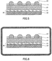
- FIG. 5 is a schematic cross-sectional view illustrating the protective tape peeling step.
- the protective tape peeling step the protective tape 10 is peeled such that the adhesive layer 11 remains and other layers are removed.
- the thermoplastic resin layer 12 and backing material film layer 13 are removed and only the adhesive layer 11 remains on the wafer 21.
- Figure 6 is a schematic cross-sectional view illustrating the curing step.
- the adhesive layer 11 is cured.
- Conventional methods of curing thermosetting type adhesive agents maybe used as a curing method and curing conditions.
- Figure 7 is a schematic cross-sectional view illustrating the dicing step.
- the wafer 21 having the adhesive tape 30 applied thereon is diced to obtain individual semiconductor chips.
- known methods such as cutting the wafer 21 apart by using a dicing saw, may be used as a dicing method.
- Figure 8 is a schematic cross-sectional view illustrating the expansion step.
- the adhesive tape 30, which has a plurality of separated semiconductor chips adhered thereon, is stretched in a radial direction and space between individual semiconductor chips is widened.
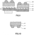
- Figure 9 is a schematic cross-sectional view illustrating the pick-up step.
- semiconductor chips adhesively secured on the adhesive tape 30 are detached by lifting up from the bottom surface of the adhesive tape 30 and detached chips are attached to a collet by suction.
- the semiconductor chips having undergone pick-up are either collected in a chip tray or conveyed to a chip-mounting nozzle of a flip-chip bonder.
- Figure 10 is a cross-sectional view illustrating the mounting step.
- the semiconductor chips are connected to a circuit substrate by using a circuit connection material such as NCF (Non Conductive Film).
- a circuit connection material such as NCF (Non Conductive Film).
- plastic substrates such as polyamide substrates, glass epoxy substrates or ceramic substrates, among others, may be used as the circuit substrate.
- plastic substrates such as polyimide substrates, glass epoxy substrates or ceramic substrates, among others, may be used as the circuit substrate.
- Known methods of using a thermal bonder or a reflow oven, among others, may be used as a connection method.
- an achievable semiconductor device includes a semiconductor chip having bump electrodes and an adhesive layer formed on a bump electrode formation surface and a circuit substrate having electrodes corresponding to the bump electrodes; excellent connection reliability properties can be achieved by forming the adhesive layer 11 on the bump electrode formation surface of the semiconductor chip.
- a protective tape was manufactured in these examples by laminating an adhesive layer and a thermoplastic resin layer.
- Semiconductor devices were manufactured by using the protective tape and sequentially performing a protective tape application step (A), a grinding step (B), an adhesive tape application step (C), a protective tape peeling step (D), a curing step (E), a dicing step (F), an expansion step (G), a pick-up step (H) and a mounting step (I). Solder bonding properties and bump embedding properties of the semiconductor device were then evaluated. It should be noted that the present invention is not limited by these examples.
- adhesive layers A1 to A3 were manufactured.
- the adhesive layer A1 was manufactured by blending a film-forming resin at 13.0 pts. mass, an epoxy resin at 54.8 pts. mass, a curing agent at 32.4 pts. mass and a curing accelerator at 0.3 pts. mass to prepare an adhesive agent composition which was then applied to a PET (polyethylene terephthalate) material treated to be detachable by using a bar coater and dried in an oven to achieve an after-drying thickness of 30. ⁇ m. Shear storage modulus of the adhesive layer A1 at 60° C was 3.3E+03 Pa.
- the adhesive layer A2 was manufactured by blending a film-forming resin at 13.0 pts. mass, an epoxy resin at 54.8 pts. mass, a curing agent at 32.4 pts. mass, a curing accelerator at 0.3 pts. mass and a filler at 25.0 pts. mass to prepare an adhesive agent composition which was then applied to a PET (polyethylene terephthalate) material treated to be detachable by using a bar coater and dried in an oven to achieve an after-drying thickness of 30 ⁇ m. Shear storage modulus of the adhesive layer A2 was 3.4E+04 Pa at 60° C.
- the adhesive layer A3 was manufactured by blending a film-forming resin at 2.0 pts. mass, an epoxy resin at 54.8 pts. mass, a curing agent at 32.4 pts. mass and a curing accelerator at 0.3 pts. mass to prepare an adhesive agent composition which was then applied to a PET (polyethylene terephthalate) material treated to be detachable by using a bar coater and dried in an oven to achieve an after-drying thickness of 30 ⁇ m. Shear storage modulus of the adhesive layer A3 was 3.6E+01 Pa at 60° C.
- Thermoplastic resin layers B1 to B3 were manufactured in the following manner.
- a thermoplastic resin described below was extrusion molded onto a PET substrate (thickness: 75 ⁇ m) to achieve a thickness of 500 ⁇ m after drying.
- Shear storage modulus of the thermoplastic resin layer B1 was 1.2E+06 Pa at 60° C
- shear storage modulus of the thermoplastic resin layer B2 was 1.4E+05 Pa at 60° C
- shear storage modulus of the thermoplastic resin layer B3 was 1.7E+07 Pa at 60° C.
- Thermoplastic resin layer B1 propylene-olefin copolymer resin (Notio PN0040 Mitsui Chemicals, Inc.)
- Thermoplastic resin layer B2 ⁇ -olefin copolymer (TAFMER P0275, Mitsui Chemicals, Inc.)
- Thermoplastic resin layer B3 linear low-density polyethylene (Novatec UF943, Japan Polyethylene Corporation)
- One of the adhesive layers A1 to A3 and one of the thermoplastic resin layers B1 to B3 were selected and laminated to manufacture protective tapes.
- a viscoelasticity measuring device was used to measure and calculate shear storage modulus G' at 60° C. Measurement conditions were set at a measurement temperature range of 0° C to 120° C, a temperature increase rate of 5° C/min, a vibration frequency of 1 Hz and a deformation of 0.1%.
- back grinding was performed to a wafer thickness of 300 ⁇ m by using a DFG8560 manufactured by DISCO Corporation.
- the protective tape was peeled such that the adhesive layer remained and other layers were removed, the adhesive layer on the wafer was cured by using an oven at a temperature of 130° C for two hours.
- the wafer was then diced and after the chips were separated, a mounter was used to mount the chips to substrates (gold electrodes with flux) and a reflow oven at a maximum temperature of 260° C was used to solder bond the chips to the substrates.
- Flux was applied to the gold electrodes on the substrates and solder wet-spreading surface area was measured at the maximum temperature of 260° C during solder bonding using the reflow oven and calculated with bump size as a reference value of 100%.
- the adhesive layer A1 and the thermoplastic resin layer B1 were laminated and a protective tape having a modulus ratio of the adhesive layer to the thermoplastic resin layer of 2.8E-03 was manufactured.
- a protective tape having a modulus ratio of the adhesive layer to the thermoplastic resin layer of 2.8E-03 was manufactured.
- a semiconductor device was manufactured by using the previously described method and evaluations were a solder bonding property of 105% and a bump embedding property of "P".
- the adhesive layer A2 and the thermoplastic resin layer B3 were laminated and a protective tape having a modulus ratio of the adhesive layer to the thermoplastic resin layer of 2.1E-03 was manufactured.
- a protective tape having a modulus ratio of the adhesive layer to the thermoplastic resin layer of 2.1E-03 was manufactured.
- a semiconductor device was manufactured by using the previously described method and evaluations were a solder bonding property of 85% and a bump embedding property of "I".
- the adhesive layer A3 and the thermoplastic resin layer B1 were laminated and a protective tape having a modulus ratio of the adhesive layer to the thermoplastic resin layer of 3.0E-05 was manufactured.
- a protective tape having a modulus ratio of the adhesive layer to the thermoplastic resin layer of 3.0E-05 was manufactured.
- a semiconductor device was manufactured by using the previously described method and evaluations were a solder bonding property of 110% and a bump embedding property of "P".
- the adhesive layer A1 and the thermoplastic resin layer B2 were laminated and a protective tape having a modulus ratio of the adhesive layer to the thermoplastic resin layer of 2.4E-02 was manufactured.
- a protective tape having a modulus ratio of the adhesive layer to the thermoplastic resin layer of 2.4E-02 was manufactured.
- a semiconductor device was manufactured by using the previously described method and evaluation was a solder bonding property of 12%.
- the adhesive layer A2 and the thermoplastic resin layer B1 were laminated and a protective tape having a modulus ratio of 3.0E-02 of the adhesive layer to the thermoplastic resin layer was manufactured.
- a protective tape having a modulus ratio of 3.0E-02 of the adhesive layer to the thermoplastic resin layer was manufactured.
- a semiconductor device was manufactured by using the previously described method and evaluation was a solder bonding property of 3%.
Landscapes
- Chemical & Material Sciences (AREA)
- Organic Chemistry (AREA)
- Mechanical Treatment Of Semiconductor (AREA)
- Adhesive Tapes (AREA)
- Dicing (AREA)
- Adhesives Or Adhesive Processes (AREA)
- Laminated Bodies (AREA)
Abstract
Description
- The present invention relates to a protective tape used in manufacturing semiconductor devices and also relates to a method for manufacturing a semiconductor device using the same. This application claims priority to
Japanese Patent Application No. 2014-088627 filed on April 22, 2014 - Conventional post-processing in manufacturing processes of flip-chip mounting semiconductors is performed in the following manner. First, adhesive sheets or tapes, which are known as back grind tape, is applied to a bump electrode formation surface of a wafer having bump electrodes formed thereon and a side opposite to the bump electrode formation surface is ground to a predetermined thickness in this configuration. After completion of the grinding, the back grind tape is peeled off and the wafer is diced to obtain individual semiconductor chips. Next, the semiconductor chips are flip-chip mounted onto other semiconductor chips or substrates. Additionally, pre-applied or post-applied type underfill is cured to reinforce the semiconductor chip.
- In recent years, there have been investigated methods using a laminated material including a thermosetting resin layer and a thermoplastic resin layer as a back grind tape wherein only the thermosetting resin layer is left on the wafer and other layers are removed (for example, see PLT 1).
- Unfortunately, in the back grind tape described above, when leaving the thermosetting resin layer on the wafer and removing the other layers, resin remaining on the bumps, for example during reflow, might obstruct solder bonding and degrade connection properties.
- PLT 1:
Japanese Unexamined Patent Application Publication No. 2005-28734 - In view of the foregoing, the object of the present invention is to provide a protective tape and a method for manufacturing a semiconductor device using the same which are capable of achieving excellent connection properties.
- To solve the aforementioned problem, a protective tape according to the present invention includes an adhesive layer, a thermoplastic resin layer and a backing material film layer in that order and a modulus ratio of a shear storage modulus of the adhesive layer to a shear storage modulus of the thermoplastic resin layer at an application temperature at which the protective tape is applied is 0.01 or less.
- Furthermore, a method for manufacturing a semiconductor device according to the present invention includes a protective tape application step of applying a protective tape having an adhesive layer onto a wafer surface having bump electrodes formed thereon, a grinding step of grinding a surface opposite to the surface of application of the protective tape and a peeling step of peeling the protective tape such that the adhesive layer remains and other layers are removed; the protective tape includes the adhesive layer, a thermoplastic resin layer, and a backing material film layer in that order, and a modulus ratio of a shear storage modulus of the adhesive layer to a shear storage modulus of the thermoplastic resin layer at an application temperature at which the protective tape is applied is 0.01 or less.
- Additionally, a semiconductor device according to the present invention is achievable by using the aforementioned method for manufacturing a semiconductor device.
- Excellent connection properties are achievable in the present invention when removing the layers other than the adhesive layer, because resin residue on bumps is suppressed by the modulus ratio of the shear storage modulus of the adhesive layer to the shear storage modulus of the thermoplastic resin layer being 0.01 or less at the application temperature.
-
-
Figure 1 is a schematic cross-sectional view illustrating a protective tape. -
Figure 2 is a schematic cross-sectional view illustrating a protective tape application step. -
Figure 3 is a schematic cross-sectional view illustrating a grinding step. -
Figure 4 is a schematic cross-sectional view illustrating an adhesive tape application step. -
Figure 5 is a schematic cross-sectional view illustrating a peeling step of a protective tape. -
Figure 6 is a schematic cross-sectional view illustrating a curing step. -
Figure 7 is a schematic cross-sectional view illustrating a dicing step. -
Figure 8 is a schematic cross-sectional view illustrating an expansion step. -
Figure 9 is a schematic cross-sectional view illustrating a pick-up step. -
Figure 10 is a schematic cross-sectional view illustrating a mounting step. - Embodiments of this invention will now be described in detail according to the following order.
- 1. Protective Tape
- 2. Method for Manufacturing a Semiconductor Device
- 3. Examples
- A protective tape according to the present invention includes an adhesive layer, a thermoplastic resin layer and a backing material film layer in that order and a modulus ratio of a shear storage modulus of the adhesive layer to a shear storage modulus of the thermoplastic resin layer at an application temperature at which the protective tape is applied is 0.01 or less and preferably 0.00001 or more and 0.005 or less. Excellent connection properties are achievable when removing the layers other than the adhesive layer, because resin residue on bumps is suppressed. One possible reason for this is that the adhesive layer having excellent deformation and fluidity properties in comparison to the thermoplastic layer can suppress the adhesion of adhesive agent to the bumps during the application of the protective tape.
-
Figure 1 is a cross-sectional schematic view illustrating the protective tape. Aprotective tape 10 is known as "back grind tape" and protects a wafer from such defects as scratches, cracks and contamination in a grinding step. As illustrated inFigure 1 , theprotective tape 10 includes anadhesive layer 11, athermoplastic resin layer 12 and a backingmaterial film layer 13 layered in that order. - A shear storage modulus of the
adhesive layer 11 at 60° C is preferably 1.0E+01 Pa or more and 1.0E+05 Pa or less. An excessively low shear storage modulus of theadhesive layer 11 leads to resin flowing while applied to a wafer and an excessively high shear storage modulus causes non-penetration of bumps. - Thickness of the
adhesive layer 11 is between 10% and 80% and preferably between 30% and 60% of the height of bump electrodes formed upon a wafer. Electrode reinforcement effects are not achievable if thickness of theadhesive layer 11 is inadequate and excessive thickness causes non-penetration of bump electrodes. - Examples of resin compositions which may be used in the
adhesive layer 11 include, without particular limitation, such thermosetting types as anionic thermosetting, cationic thermosetting and radical thermosetting types and such photosetting types as cationic photosetting and radical photosetting types or a combination of these thermosetting/photosetting types may be used in approximately the same manner. - A thermosetting adhesive agent composition including film-forming resins, epoxy resins, curing agents and curing accelerators used as the
adhesive layer 11 will now be explained. - As a film-forming resin, a variety of resins including phenoxy resins, epoxy resins, modified epoxy resins and urethane resins, among others, may be used. These film-forming resins may be used individually or in a combination of two or more types. Among these, in view of film-formed state and connection reliability properties, among others, a phenoxy resin is preferably used.
- Examples of epoxy resins that may be used include dicyclopentadiene epoxy resins, glycidylether epoxy resins, glycidylamine epoxy resins, bisphenol A epoxy resins, bisphenol F epoxy resins, bisphenol S epoxy resins, epoxy resins having a spiroring, naphthalene epoxy resins, biphenyl epoxy resins, terpene epoxy resins, tetrabromobisphenol A epoxy resins, cresol novolac epoxy resins, phenol novolac epoxy resins, α-naphthalene novolac epoxy resins and brominated phenol novolac epoxy resins. These epoxy resins may be used individually or in a combination of two or more types. Among these, in view of high adhesiveness and heat resistance properties, a dicyclopentadiene epoxy resin is preferably used.
- Examples of curing agents that may be used include novolac phenol resins, aliphatic amines, aromatic amines and acid anhydrides; these curing agents may be used individually or in a combination of two or more types. Among these, in view of crosslink density in a cured resin, a novolac phenol resin is preferably used.
- Examples of curing accelerators that may be used include imidazoles such as 2-methylimidazole, 2-ethylimidazole and 2-ethyl-4-methylimidazole, tertiary amines such as 1,8-Diazabicyclo[5.4.0]undec-7-ene (DBU) and 2-(dimethylaminomethyl) phenol, phosphines such as triphenylphosphine, and metallic compounds such as stannous octoate.
- Additionally, other constituents such as inorganic fillers, silane coupling agents, elastomers such as acrylic rubber and pigments such as carbon black may be blended to the adhesive agent composition according to purpose.
- Examples of the
thermoplastic layer 12 include ethylene vinyl acetate (EVA), polyethylene, polypropylene, polyamide, polyacetal, polyethylene terephthalate, polybutylene terephthalate, fluororesins, polyphenylene sulfide, polystyrene, ABS resin, acrylic based resins, polycarbonate, polyurethane, polyvinyl chloride and polyphenylene oxide, among others; these may be used individually or in a combination of two or more. - Additionally, the shear storage modulus of the
thermoplastic layer 12 at 60° C is preferably 1.0E+07 Pa or less. Bump embedding properties of theadhesive layer 11 can be improved by thethermoplastic resin layer 12 having a shear storage modulus at 60° C of 1.0E+07 or less. - Materials that may be used as the backing
material film layer 13 include plastic films such as polyethylene terephthalate, polyethylene, polypropylene and polyester and porous backing materials such as those made from paper, cloth and/or non-woven fabric. - It should be noted that the protective tape is not limited to the composition described above and one or more other layers may be formed on a surface of any layer and/or between any adjacent layers.
- Excellent connection properties are achievable with such a protective tape because adhesion of adhesive agent to bumps is suppressed during application to a wafer. Furthermore, bump electrodes can be reinforced by curing the adhesive layer because embedding conditions of the adhesive layer between bumps are favorable.
- A method for manufacturing a semiconductor device using the aforementioned protective tape will now be described. A method for manufacturing a semiconductor device according to this embodiment includes a protective tape application step of applying a protective tape having an adhesive layer onto a wafer surface having bump electrodes formed thereon, a grinding step of grinding a surface opposite to the surface of application of the protective tape, a peeling step of peeling the protective tape such that the adhesive layer remains and other layers are removed, wherein the protective tape includes the adhesive layer, a thermoplastic resin layer and a backing material film layer in that order, and a modulus ratio of a shear storage modulus of the adhesive layer to a shear storage modulus of the thermoplastic resin layer at an application temperature at which the protective tape is applied is 0.01 or less. A curing step of curing the adhesive layer may be performed before the grinding step, an adhesive tape application step or a dicing step.
- An embodiment of the method for manufacturing a semiconductor device will now be described. In this embodiment of the method for manufacturing a semiconductor device, the protective tape is used and the curing step is performed between the adhesive tape application step and the dicing step. Thus, this embodiment of the method for manufacturing a semiconductor device includes a protective tape application step (A), a grinding step (B), an adhesive tape application step (C), a protective tape peeling step (D), a curing step (E) of curing the adhesive layer, a dicing step (F), an expansion step (G), a pick-up step (H) and a mounting step (I).
-
Figure 2 is a schematic cross-sectional view illustrating the protective tape application step. In the protective tape application step, theprotective tape 10 is applied to a surface of awafer 21 havingbump electrodes 22 formed thereon. An application temperature at which theprotective tape 10 is applied is between 25° C and 100° C and preferably between 40° C and 80° C in view of reducing voids, improving adhesion to the wafer and preventing warping after wafer grinding. - The
wafer 21 includes an integrated circuit formed on a semiconductor surface made from such materials as silicon, and thebump electrodes 22, which are for making connections and are known as bumps. Thickness of thewafer 21 is not particularly limited but is preferably 200 to 1000 µm. - Without particular limitation, examples of the
bump electrodes 22 include solder-containing low-melt-point bumps and high-melt-point bumps including tin bumps, silver-tin bumps, silver-tin-copper bumps, gold bumps and copper bumps. Height of thebump electrodes 22 is not particularly limited but is preferably between 10 and 200 µm. - The
protective tape 10 is applied so that theadhesive layer 11 is in contact with the surface side on which thebump electrodes 22 have been formed. Because thickness of theadhesive layer 11 of theprotective tape 10 is between 10% and 80% of thebump electrodes 22, thebump electrodes 22 penetrate theadhesive layer 11 and embed in thethermoplastic resin layer 12. -
Figure 3 is a schematic cross-sectional view illustrating the grinding step. In the grinding step, grinding is performed on a side opposite to the side of application of theprotective tape 10. The side of thewafer 21 opposite to the side of application of theprotective tape 10 is secured to a grinding device and is ground. Grinding is typically performed on thewafer 21 to a thickness of between 50 µm and 600 µm; however, in this embodiment, grinding may be performed to a thickness of 50 µm or less because theadhesive layer 11 reinforces thebump electrodes 22. -
Figure 4 is a schematic cross-sectional view illustrating the adhesive tape application step. In the adhesive tape application step, anadhesive tape 30 is applied onto the surface that was ground. Theadhesive tape 30, which is known as dicing tape, is a tape for protecting and securing thewafer 21 in the dicing step (F) and retaining thewafer 21 until the pick-up step (H). - Without particular limitation, known materials may be used as the
adhesive tape 30. Theadhesive tape 30 typically includes anadhesive layer 31 and a backingmaterial film layer 32. Examples of adhesives which may be used in theadhesive layer 31 include polyethylene types, acrylic types, rubber types and urethane types, among others. Plastic films such as polyethylene terephthalate, polyethylene, polypropylene and polyester and porous backing materials such as those made from paper, cloth and/or non-woven fabrics may be used as the backingmaterial film layer 32. Adhesive tape application device and conditions are without particular limitations and known devices and conditions may be used. -
Figure 5 is a schematic cross-sectional view illustrating the protective tape peeling step. In the protective tape peeling step, theprotective tape 10 is peeled such that theadhesive layer 11 remains and other layers are removed. Thus, thethermoplastic resin layer 12 and backingmaterial film layer 13 are removed and only theadhesive layer 11 remains on thewafer 21. -
Figure 6 is a schematic cross-sectional view illustrating the curing step. In the curing step, theadhesive layer 11 is cured. Conventional methods of curing thermosetting type adhesive agents maybe used as a curing method and curing conditions. -
Figure 7 is a schematic cross-sectional view illustrating the dicing step. In the dicing step, thewafer 21 having theadhesive tape 30 applied thereon is diced to obtain individual semiconductor chips. Without particular limitation, known methods, such as cutting thewafer 21 apart by using a dicing saw, may be used as a dicing method. -
Figure 8 is a schematic cross-sectional view illustrating the expansion step. In the expansion step, for example, theadhesive tape 30, which has a plurality of separated semiconductor chips adhered thereon, is stretched in a radial direction and space between individual semiconductor chips is widened. -
Figure 9 is a schematic cross-sectional view illustrating the pick-up step. In the pick-up step, semiconductor chips adhesively secured on theadhesive tape 30 are detached by lifting up from the bottom surface of theadhesive tape 30 and detached chips are attached to a collet by suction. The semiconductor chips having undergone pick-up are either collected in a chip tray or conveyed to a chip-mounting nozzle of a flip-chip bonder. -
Figure 10 is a cross-sectional view illustrating the mounting step. In the mounting step, for example, the semiconductor chips are connected to a circuit substrate by using a circuit connection material such as NCF (Non Conductive Film). Without particular limitation, plastic substrates such as polyamide substrates, glass epoxy substrates or ceramic substrates, among others, may be used as the circuit substrate. Without particular limitation, plastic substrates such as polyimide substrates, glass epoxy substrates or ceramic substrates, among others, may be used as the circuit substrate. Known methods of using a thermal bonder or a reflow oven, among others, may be used as a connection method. - In such a method for manufacturing a semiconductor device, damage to bump electrodes in such post-processing steps as the dicing, pick-up and mounting steps can be reduced because the bump electrodes are reinforced by curing the adhesive layer before the dicing step on the wafer surface having the bump electrodes formed thereon. Thus, high yield rates of semiconductor devices having excellent connection reliability properties are achievable. Furthermore, an achievable semiconductor device includes a semiconductor chip having bump electrodes and an adhesive layer formed on a bump electrode formation surface and a circuit substrate having electrodes corresponding to the bump electrodes; excellent connection reliability properties can be achieved by forming the
adhesive layer 11 on the bump electrode formation surface of the semiconductor chip. Examples - Examples of the present invention are explained below. A protective tape was manufactured in these examples by laminating an adhesive layer and a thermoplastic resin layer. Semiconductor devices were manufactured by using the protective tape and sequentially performing a protective tape application step (A), a grinding step (B), an adhesive tape application step (C), a protective tape peeling step (D), a curing step (E), a dicing step (F), an expansion step (G), a pick-up step (H) and a mounting step (I). Solder bonding properties and bump embedding properties of the semiconductor device were then evaluated. It should be noted that the present invention is not limited by these examples.
- As presented in Table 1, adhesive layers A1 to A3 were manufactured. The adhesive layer A1 was manufactured by blending a film-forming resin at 13.0 pts. mass, an epoxy resin at 54.8 pts. mass, a curing agent at 32.4 pts. mass and a curing accelerator at 0.3 pts. mass to prepare an adhesive agent composition which was then applied to a PET (polyethylene terephthalate) material treated to be detachable by using a bar coater and dried in an oven to achieve an after-drying thickness of 30. µm. Shear storage modulus of the adhesive layer A1 at 60° C was 3.3E+03 Pa.
- The adhesive layer A2 was manufactured by blending a film-forming resin at 13.0 pts. mass, an epoxy resin at 54.8 pts. mass, a curing agent at 32.4 pts. mass, a curing accelerator at 0.3 pts. mass and a filler at 25.0 pts. mass to prepare an adhesive agent composition which was then applied to a PET (polyethylene terephthalate) material treated to be detachable by using a bar coater and dried in an oven to achieve an after-drying thickness of 30 µm. Shear storage modulus of the adhesive layer A2 was 3.4E+04 Pa at 60° C.
- The adhesive layer A3 was manufactured by blending a film-forming resin at 2.0 pts. mass, an epoxy resin at 54.8 pts. mass, a curing agent at 32.4 pts. mass and a curing accelerator at 0.3 pts. mass to prepare an adhesive agent composition which was then applied to a PET (polyethylene terephthalate) material treated to be detachable by using a bar coater and dried in an oven to achieve an after-drying thickness of 30 µm. Shear storage modulus of the adhesive layer A3 was 3.6E+01 Pa at 60° C.
Table 1 A1 A2 A3 Film-Forming resin 13.0 13.0 2.0 Epoxy resin 84.8 54.8 54.8 Curing agent 32.4 32.4 32.4 Curing accelerator 0.3 0.3 0.3 Filler - 25.0 - Total 100.0 125.0 89.0 Filler amount [wt%] - 20.0 - Compressive elastic modulus [Pa] 3.30E+03 3.60E+04 3.60E+01 -
- Film forming resin: phenoxy resin (PKHH, Union Carbide Corporation)
- Epoxy resin: sicyclopentadiene epoxy resin (HP7200H, DIC Corporation)
- Curing agent: novolac phenol resin (TD-2093 DIC Corporation)
- Curing accelerator: 2-ethyl-4-methylimidazole (2E4MZ)
- Filler: silica (Aerosil RY 200, Nippon Aerosil Co., Ltd.)
- Thermoplastic resin layers B1 to B3 were manufactured in the following manner. A thermoplastic resin described below was extrusion molded onto a PET substrate (thickness: 75 µm) to achieve a thickness of 500 µm after drying. Shear storage modulus of the thermoplastic resin layer B1 was 1.2E+06 Pa at 60° C, shear storage modulus of the thermoplastic resin layer B2 was 1.4E+05 Pa at 60° C and shear storage modulus of the thermoplastic resin layer B3 was 1.7E+07 Pa at 60° C.
- Thermoplastic resin layer B1: propylene-olefin copolymer resin (Notio PN0040 Mitsui Chemicals, Inc.)
- Thermoplastic resin layer B2: α-olefin copolymer (TAFMER P0275, Mitsui Chemicals, Inc.)
- Thermoplastic resin layer B3: linear low-density polyethylene (Novatec UF943, Japan Polyethylene Corporation)
- One of the adhesive layers A1 to A3 and one of the thermoplastic resin layers B1 to B3 were selected and laminated to manufacture protective tapes.
- A viscoelasticity measuring device was used to measure and calculate shear storage modulus G' at 60° C. Measurement conditions were set at a measurement temperature range of 0° C to 120° C, a temperature increase rate of 5° C/min, a vibration frequency of 1 Hz and a deformation of 0.1%.
- The adhesive layer surface of the protective tape was applied onto a wafer (size: 5 cm x 5 cm x 725 µ mt) having solder bumps (Φ = 250 µm, H = 200 µm, pitch = 250 µm) formed thereon and lamination was performed at 60° C by using a vacuum type laminator.
- Next, back grinding was performed to a wafer thickness of 300 µm by using a DFG8560 manufactured by DISCO Corporation. Subsequently, the protective tape was peeled such that the adhesive layer remained and other layers were removed, the adhesive layer on the wafer was cured by using an oven at a temperature of 130° C for two hours. The wafer was then diced and after the chips were separated, a mounter was used to mount the chips to substrates (gold electrodes with flux) and a reflow oven at a maximum temperature of 260° C was used to solder bond the chips to the substrates.
- Flux was applied to the gold electrodes on the substrates and solder wet-spreading surface area was measured at the maximum temperature of 260° C during solder bonding using the reflow oven and calculated with bump size as a reference value of 100%.
- A microscope (100x) was used for observation and products not having gaps between the adhesive layer and the bumps were evaluated as passing, hereinafter denoted as "P", and products having such gaps were evaluated as irregular, hereinafter denoted as "I". It should be noted that the bump embedding property was evaluated only in samples having a solder bonding property evaluation of 80% or more.
- As presented in Table 2, the adhesive layer A1 and the thermoplastic resin layer B1 were laminated and a protective tape having a modulus ratio of the adhesive layer to the thermoplastic resin layer of 2.8E-03 was manufactured. Using this protective tape, a semiconductor device was manufactured by using the previously described method and evaluations were a solder bonding property of 105% and a bump embedding property of "P".
- As presented in Table 2, the adhesive layer A2 and the thermoplastic resin layer B3 were laminated and a protective tape having a modulus ratio of the adhesive layer to the thermoplastic resin layer of 2.1E-03 was manufactured. Using this protective tape, a semiconductor device was manufactured by using the previously described method and evaluations were a solder bonding property of 85% and a bump embedding property of "I".
- As presented in Table 2, the adhesive layer A3 and the thermoplastic resin layer B1 were laminated and a protective tape having a modulus ratio of the adhesive layer to the thermoplastic resin layer of 3.0E-05 was manufactured. Using this protective tape, a semiconductor device was manufactured by using the previously described method and evaluations were a solder bonding property of 110% and a bump embedding property of "P".
- As presented in Table 2, the adhesive layer A1 and the thermoplastic resin layer B2 were laminated and a protective tape having a modulus ratio of the adhesive layer to the thermoplastic resin layer of 2.4E-02 was manufactured. Using this protective tape, a semiconductor device was manufactured by using the previously described method and evaluation was a solder bonding property of 12%.
- As presented in Table 2, the adhesive layer A2 and the thermoplastic resin layer B1 were laminated and a protective tape having a modulus ratio of 3.0E-02 of the adhesive layer to the thermoplastic resin layer was manufactured. Using this protective tape, a semiconductor device was manufactured by using the previously described method and evaluation was a solder bonding property of 3%.
Table 2 Ex.1 Ex.2 Ex.3 Com.1 Com.2 Adhesive layer A1 A2 A3 A1 A2 Thermoplastic resin B1 B3 B1 B2 B1 60°C compressive elastic modulus Adhesive layer [Pa] 3.3E+03 3.6E+04 3.6E+01 3.3E+03 3.6E+04 Thermoplastic resin [Pa] 1.2E+06 1.7E+07 1.2E+06 1.4E+05 1.2E+06 Compressive elastic modulus ratio (A/B) 2.8E-03 2.1E-03 3.0E-05 2.4E-02 3.0E-02 Solder bonding property [%] 105 85 110 12 3 Bump embedding property P I P - - - As in the Comparative Examples 1 and 2, a good solder bonding property was not achievable in cases where the modulus ratio (A/B) exceeded 0.01 at 60° C. In contrast, as in the Comparative Examples 1 to 3, a good bonding property was obtainable in cases where the modulus ratio (A/B) was 0.01 or less at 60° C. Furthermore, as in the Examples 1 and 3, it was found that good bump embedding properties were obtainable by a shear storage modulus of the thermoplastic resin layer at 60° C being 1.0E+07 Pa or less.
- 10 protective tape, 11 adhesive layer, 12 thermoplastic resin layer, 13 backing material film layer, 21 wafer, 22 bump electrodes, 30 adhesive tape, 31 adhesive layer, 32 backing material film layer
Claims (11)
- A protective tape comprising an adhesive layer, a thermoplastic resin layer and a backing material film layer in that order;wherein a modulus ratio of a shear storage modulus of the adhesive layer to a shear storage modulus of the thermoplastic resin layer at an application temperature at which the protective tape is applied is 0.01 or less.
- The protective tape according to claim 1, wherein the application temperature is between 40° C and 80° C.
- The protective tape according to claim 1 or 2, wherein the shear storage modulus of the thermoplastic resin layer at 60° C is 1.0E+07 Pa or less.
- The protective tape according to claim 1 or 2, wherein the shear storage modulus of the adhesive layer at 60° C is between 1.0E+01 Pa and 1.0E+05 Pa.
- The protective tape according to claim 3, wherein the shear storage modulus of the adhesive layer at 60° C is between 1.0E+01 Pa and 1.0E+05 Pa.
- The protective tape according to claim 1 or 2, wherein the adhesive layer is applied onto a wafer surface having a bump electrode formed thereon; and
a thickness of the adhesive layer is between 10% and 80% relative to a height of the bump electrode. - The protective tape according to claim 3, wherein the adhesive layer is applied onto a wafer surface having a bump electrode formed thereon; and
a thickness of the adhesive layer is between 10% and 80% relative to a height of the bump electrode. - The protective tape according to claim 4, wherein the adhesive layer is applied onto a wafer surface having a bump electrode formed thereon; and
a thickness of the adhesive layer is between 10% and 80% relative to a height of the bump electrode. - A method for manufacturing a semiconductor device comprising:a protective tape application step of applying a protective tape having an adhesive layer onto a wafer surface having a bump electrode formed thereon;a grinding step of grinding a surface opposite to a surface of application of the protective tape; anda peeling step of peeling the protective tape such that the adhesive layer remains and other layers are removed;wherein the protective tape comprises an adhesive layer, a thermoplastic resin layer and a backing material film layer in that order, and a modulus ratio of a shear storage modulus of the adhesive layer to a shear storage modulus of the thermoplastic resin layer at an application temperature at which the protective tape is applied is 0.01 or less.
- The method for manufacturing a semiconductor device according to claim 9 further comprising:an adhesive tape application step of applying an adhesive tape onto a surface on which grinding was performed;a dicing step of dicing the wafer having the adhesive tape applied thereon into individual semiconductor chips; anda curing step of curing the adhesive layer;wherein the curing step is performed before the dicing step.
- A semiconductor device manufactured by the method for manufacturing a semiconductor device according to claim 9 or 10.
Applications Claiming Priority (2)
| Application Number | Priority Date | Filing Date | Title |
|---|---|---|---|
| JP2014088627A JP6347657B2 (en) | 2014-04-22 | 2014-04-22 | Protective tape and method of manufacturing semiconductor device using the same |
| PCT/JP2014/071532 WO2015162808A1 (en) | 2014-04-22 | 2014-08-18 | Protective tape and semiconductor device manufacturing method using same |
Publications (3)
| Publication Number | Publication Date |
|---|---|
| EP2985328A1 true EP2985328A1 (en) | 2016-02-17 |
| EP2985328A4 EP2985328A4 (en) | 2017-03-08 |
| EP2985328B1 EP2985328B1 (en) | 2020-07-15 |
Family
ID=54331994
Family Applications (1)
| Application Number | Title | Priority Date | Filing Date |
|---|---|---|---|
| EP14890441.0A Active EP2985328B1 (en) | 2014-04-22 | 2014-08-18 | Protective tape and semiconductor device manufacturing method using same |
Country Status (7)
| Country | Link |
|---|---|
| US (1) | US9741598B2 (en) |
| EP (1) | EP2985328B1 (en) |
| JP (1) | JP6347657B2 (en) |
| KR (1) | KR102280578B1 (en) |
| CN (1) | CN105339450B (en) |
| TW (1) | TWI624369B (en) |
| WO (1) | WO2015162808A1 (en) |
Cited By (1)
| Publication number | Priority date | Publication date | Assignee | Title |
|---|---|---|---|---|
| EP3352204A4 (en) * | 2015-11-04 | 2019-03-20 | Lintec Corporation | Curable resin film and first protective film forming sheet |
Families Citing this family (24)
| Publication number | Priority date | Publication date | Assignee | Title |
|---|---|---|---|---|
| JP6243764B2 (en) * | 2014-03-18 | 2017-12-06 | デクセリアルズ株式会社 | Method for manufacturing flexible mounting module body |
| JP6599134B2 (en) * | 2015-06-04 | 2019-10-30 | デクセリアルズ株式会社 | Protective tape and method of manufacturing semiconductor device using the same |
| WO2017077957A1 (en) * | 2015-11-04 | 2017-05-11 | リンテック株式会社 | Method for manufacturing semiconductor device |
| TWI641494B (en) | 2015-11-04 | 2018-11-21 | 日商琳得科股份有限公司 | First protective film forming sheet, first protective film forming method, and semiconductor wafer manufacturing method |
| JP6816918B2 (en) * | 2015-11-04 | 2021-01-20 | リンテック株式会社 | Manufacturing method of semiconductor devices |
| WO2017078042A1 (en) * | 2015-11-04 | 2017-05-11 | リンテック株式会社 | Protective film forming sheet |
| WO2017077809A1 (en) * | 2015-11-04 | 2017-05-11 | リンテック株式会社 | Method for manufacturing semiconductor device |
| CN108292178B (en) * | 2015-11-26 | 2022-03-22 | 阪东化学株式会社 | Optically transparent adhesive sheet, method for producing optically transparent adhesive sheet, laminate, and display device with touch panel |
| CN106206397B (en) * | 2016-08-05 | 2020-02-07 | 厦门市三安光电科技有限公司 | Film for semiconductor device and method for manufacturing semiconductor device |
| SG11201902955QA (en) | 2016-10-05 | 2019-05-30 | Lintec Corp | First protective film forming sheet |
| JP6821392B2 (en) * | 2016-10-27 | 2021-01-27 | デクセリアルズ株式会社 | Manufacturing method of protective tape and semiconductor device |
| JP6820724B2 (en) * | 2016-11-18 | 2021-01-27 | 積水化学工業株式会社 | Semiconductor device manufacturing method and protective tape |
| JP6975006B2 (en) * | 2016-12-26 | 2021-12-01 | リンテック株式会社 | Work manufacturing method |
| KR101877897B1 (en) * | 2017-03-06 | 2018-07-12 | 엘비세미콘 주식회사 | Methods of fabricating bump structure |
| KR102387943B1 (en) * | 2017-05-17 | 2022-04-18 | 린텍 가부시키가이샤 | Semiconductor device and method for manufacturing same |
| WO2019044623A1 (en) * | 2017-08-29 | 2019-03-07 | 積水化学工業株式会社 | Adhesive composition, adhesive tape, and method for protecting semiconductor device |
| JP7042437B2 (en) * | 2017-09-07 | 2022-03-28 | パナソニックIpマネジメント株式会社 | Method of manufacturing element chips |
| CN111801567B (en) * | 2018-03-06 | 2023-08-11 | 株式会社力森诺科 | Method for evaluating fluidity of resin composition, method for sorting resin composition, and method for manufacturing semiconductor device |
| TWI825080B (en) * | 2018-03-30 | 2023-12-11 | 日商琳得科股份有限公司 | Method for manufacturing semiconductor chip |
| JP7614781B2 (en) * | 2020-10-19 | 2025-01-16 | 日東電工株式会社 | Semiconductor device manufacturing method |
| KR20230088752A (en) | 2020-10-19 | 2023-06-20 | 쓰리엠 이노베이티브 프로퍼티즈 컴파니 | Masking tapes, articles therefrom, and methods of making and using the same |
| JP7825427B2 (en) * | 2022-01-12 | 2026-03-06 | リンテック株式会社 | Sheet for forming first protective film, method for manufacturing semiconductor device, and use of the sheet |
| JP7772602B2 (en) * | 2022-01-12 | 2025-11-18 | リンテック株式会社 | Sheet for forming first protective film, method for manufacturing semiconductor device, and use of the sheet |
| JP2025154781A (en) | 2024-03-29 | 2025-10-10 | リンテック株式会社 | Film for forming protective film, composite sheet for forming protective film, method for manufacturing semiconductor device, and semiconductor device |
Family Cites Families (9)
| Publication number | Priority date | Publication date | Assignee | Title |
|---|---|---|---|---|
| JP4170839B2 (en) | 2003-07-11 | 2008-10-22 | 日東電工株式会社 | Laminated sheet |
| JP4776189B2 (en) | 2004-08-03 | 2011-09-21 | 古河電気工業株式会社 | Wafer processing tape |
| US20090075429A1 (en) * | 2005-04-27 | 2009-03-19 | Lintec Corporation | Sheet-Like Underfill Material and Semiconductor Device Manufacturing Method |
| MY165350A (en) * | 2010-06-02 | 2018-03-21 | Mitsui Chemicals Tohcello Inc | Sheet for protecting surface of semiconductor wafer, semiconductor device manufacturing method and semiconductor wafer protection method using sheet |
| JP5385988B2 (en) | 2010-08-23 | 2014-01-08 | 積水化学工業株式会社 | Adhesive sheet and semiconductor chip mounting method |
| JP2012074623A (en) | 2010-09-29 | 2012-04-12 | Sekisui Chem Co Ltd | Adhesive film for processing semiconductor, and method of manufacturing semiconductor chip mounting body |
| JP5830250B2 (en) * | 2011-02-15 | 2015-12-09 | 日東電工株式会社 | Manufacturing method of semiconductor device |
| JP5951216B2 (en) * | 2011-10-13 | 2016-07-13 | リンテック株式会社 | Adhesive sheet and method of using the same |
| JP5242830B1 (en) * | 2012-07-06 | 2013-07-24 | 古河電気工業株式会社 | Adhesive tape for protecting semiconductor wafer surface and method for producing semiconductor wafer |
-
2014
- 2014-04-22 JP JP2014088627A patent/JP6347657B2/en active Active
- 2014-08-15 TW TW103128014A patent/TWI624369B/en active
- 2014-08-18 CN CN201480009023.7A patent/CN105339450B/en active Active
- 2014-08-18 US US14/761,913 patent/US9741598B2/en active Active
- 2014-08-18 KR KR1020157023078A patent/KR102280578B1/en active Active
- 2014-08-18 WO PCT/JP2014/071532 patent/WO2015162808A1/en not_active Ceased
- 2014-08-18 EP EP14890441.0A patent/EP2985328B1/en active Active
Cited By (2)
| Publication number | Priority date | Publication date | Assignee | Title |
|---|---|---|---|---|
| EP3352204A4 (en) * | 2015-11-04 | 2019-03-20 | Lintec Corporation | Curable resin film and first protective film forming sheet |
| US11781033B2 (en) | 2015-11-04 | 2023-10-10 | Lintec Corporation | Method of forming first protective film |
Also Published As
| Publication number | Publication date |
|---|---|
| KR102280578B1 (en) | 2021-07-23 |
| EP2985328A4 (en) | 2017-03-08 |
| JP6347657B2 (en) | 2018-06-27 |
| JP2015206006A (en) | 2015-11-19 |
| TW201540507A (en) | 2015-11-01 |
| WO2015162808A1 (en) | 2015-10-29 |
| EP2985328B1 (en) | 2020-07-15 |
| TWI624369B (en) | 2018-05-21 |
| US9741598B2 (en) | 2017-08-22 |
| CN105339450A (en) | 2016-02-17 |
| US20160181140A1 (en) | 2016-06-23 |
| KR20160143486A (en) | 2016-12-14 |
| CN105339450B (en) | 2022-05-24 |
Similar Documents
| Publication | Publication Date | Title |
|---|---|---|
| EP2985328B1 (en) | Protective tape and semiconductor device manufacturing method using same | |
| KR101140512B1 (en) | Thermosetting die bonding film | |
| KR101010418B1 (en) | Dicing Die Bond Film | |
| US10483148B2 (en) | Protective tape and method for manufacturing semiconductor device | |
| US10312125B2 (en) | Protective tape and method for manufacturing semiconductor device using the same | |
| US20110084408A1 (en) | Thermosetting die-bonding film | |
| KR20110036698A (en) | Manufacturing method of dicing die bond film | |
| KR20160002714A (en) | Thermosetting resin composition and semiconductor device manufacturing method | |
| JP5828881B2 (en) | Adhesive film, dicing die bond film, semiconductor device manufacturing method, and semiconductor device | |
| CN108178990A (en) | Adhering film, dicing/die bonding film, the manufacturing method of semiconductor device and semiconductor device | |
| KR20160055807A (en) | Method for producing semiconductor device | |
| KR20210003352A (en) | Fod adhesive film and semiconductor package comprising thereof | |
| US20160233184A1 (en) | Semiconductor Device Manufacturing Method | |
| JP6821392B2 (en) | Manufacturing method of protective tape and semiconductor device |
Legal Events
| Date | Code | Title | Description |
|---|---|---|---|
| PUAI | Public reference made under article 153(3) epc to a published international application that has entered the european phase |
Free format text: ORIGINAL CODE: 0009012 |
|
| 17P | Request for examination filed |
Effective date: 20151112 |
|
| AK | Designated contracting states |
Kind code of ref document: A1 Designated state(s): AL AT BE BG CH CY CZ DE DK EE ES FI FR GB GR HR HU IE IS IT LI LT LU LV MC MK MT NL NO PL PT RO RS SE SI SK SM TR |
|
| AX | Request for extension of the european patent |
Extension state: BA ME |
|
| A4 | Supplementary search report drawn up and despatched |
Effective date: 20170203 |
|
| RIC1 | Information provided on ipc code assigned before grant |
Ipc: H01L 21/78 20060101ALI20170130BHEP Ipc: H01L 23/31 20060101ALI20170130BHEP Ipc: H01L 21/301 20060101ALI20170130BHEP Ipc: H01L 21/304 20060101ALI20170130BHEP Ipc: C09J 7/02 20060101AFI20170130BHEP Ipc: H01L 21/683 20060101ALI20170130BHEP Ipc: B32B 27/00 20060101ALI20170130BHEP |
|
| DAX | Request for extension of the european patent (deleted) | ||
| STAA | Information on the status of an ep patent application or granted ep patent |
Free format text: STATUS: EXAMINATION IS IN PROGRESS |
|
| 17Q | First examination report despatched |
Effective date: 20190916 |
|
| REG | Reference to a national code |
Ref country code: DE Ref legal event code: R079 Ref document number: 602014067889 Country of ref document: DE Free format text: PREVIOUS MAIN CLASS: C09J0007020000 Ipc: C09J0007350000 |
|
| GRAP | Despatch of communication of intention to grant a patent |
Free format text: ORIGINAL CODE: EPIDOSNIGR1 |
|
| RIC1 | Information provided on ipc code assigned before grant |
Ipc: H01L 21/301 20060101ALI20200129BHEP Ipc: C09J 7/35 20180101AFI20200129BHEP Ipc: C09J 7/29 20180101ALI20200129BHEP |
|
| STAA | Information on the status of an ep patent application or granted ep patent |
Free format text: STATUS: GRANT OF PATENT IS INTENDED |
|
| INTG | Intention to grant announced |
Effective date: 20200305 |
|
| GRAS | Grant fee paid |
Free format text: ORIGINAL CODE: EPIDOSNIGR3 |
|
| GRAA | (expected) grant |
Free format text: ORIGINAL CODE: 0009210 |
|
| STAA | Information on the status of an ep patent application or granted ep patent |
Free format text: STATUS: THE PATENT HAS BEEN GRANTED |
|
| AK | Designated contracting states |
Kind code of ref document: B1 Designated state(s): AL AT BE BG CH CY CZ DE DK EE ES FI FR GB GR HR HU IE IS IT LI LT LU LV MC MK MT NL NO PL PT RO RS SE SI SK SM TR |
|
| REG | Reference to a national code |
Ref country code: GB Ref legal event code: FG4D Ref country code: CH Ref legal event code: EP |
|
| REG | Reference to a national code |
Ref country code: IE Ref legal event code: FG4D |
|
| REG | Reference to a national code |
Ref country code: DE Ref legal event code: R096 Ref document number: 602014067889 Country of ref document: DE |
|
| REG | Reference to a national code |
Ref country code: AT Ref legal event code: REF Ref document number: 1291024 Country of ref document: AT Kind code of ref document: T Effective date: 20200815 |
|
| REG | Reference to a national code |
Ref country code: NL Ref legal event code: FP |
|
| REG | Reference to a national code |
Ref country code: LT Ref legal event code: MG4D |
|
| REG | Reference to a national code |
Ref country code: AT Ref legal event code: MK05 Ref document number: 1291024 Country of ref document: AT Kind code of ref document: T Effective date: 20200715 |
|
| PG25 | Lapsed in a contracting state [announced via postgrant information from national office to epo] |
Ref country code: HR Free format text: LAPSE BECAUSE OF FAILURE TO SUBMIT A TRANSLATION OF THE DESCRIPTION OR TO PAY THE FEE WITHIN THE PRESCRIBED TIME-LIMIT Effective date: 20200715 Ref country code: ES Free format text: LAPSE BECAUSE OF FAILURE TO SUBMIT A TRANSLATION OF THE DESCRIPTION OR TO PAY THE FEE WITHIN THE PRESCRIBED TIME-LIMIT Effective date: 20200715 Ref country code: NO Free format text: LAPSE BECAUSE OF FAILURE TO SUBMIT A TRANSLATION OF THE DESCRIPTION OR TO PAY THE FEE WITHIN THE PRESCRIBED TIME-LIMIT Effective date: 20201015 Ref country code: GR Free format text: LAPSE BECAUSE OF FAILURE TO SUBMIT A TRANSLATION OF THE DESCRIPTION OR TO PAY THE FEE WITHIN THE PRESCRIBED TIME-LIMIT Effective date: 20201016 Ref country code: AT Free format text: LAPSE BECAUSE OF FAILURE TO SUBMIT A TRANSLATION OF THE DESCRIPTION OR TO PAY THE FEE WITHIN THE PRESCRIBED TIME-LIMIT Effective date: 20200715 Ref country code: BG Free format text: LAPSE BECAUSE OF FAILURE TO SUBMIT A TRANSLATION OF THE DESCRIPTION OR TO PAY THE FEE WITHIN THE PRESCRIBED TIME-LIMIT Effective date: 20201015 Ref country code: SE Free format text: LAPSE BECAUSE OF FAILURE TO SUBMIT A TRANSLATION OF THE DESCRIPTION OR TO PAY THE FEE WITHIN THE PRESCRIBED TIME-LIMIT Effective date: 20200715 Ref country code: FI Free format text: LAPSE BECAUSE OF FAILURE TO SUBMIT A TRANSLATION OF THE DESCRIPTION OR TO PAY THE FEE WITHIN THE PRESCRIBED TIME-LIMIT Effective date: 20200715 Ref country code: PT Free format text: LAPSE BECAUSE OF FAILURE TO SUBMIT A TRANSLATION OF THE DESCRIPTION OR TO PAY THE FEE WITHIN THE PRESCRIBED TIME-LIMIT Effective date: 20201116 Ref country code: LT Free format text: LAPSE BECAUSE OF FAILURE TO SUBMIT A TRANSLATION OF THE DESCRIPTION OR TO PAY THE FEE WITHIN THE PRESCRIBED TIME-LIMIT Effective date: 20200715 |
|
| PG25 | Lapsed in a contracting state [announced via postgrant information from national office to epo] |
Ref country code: IS Free format text: LAPSE BECAUSE OF FAILURE TO SUBMIT A TRANSLATION OF THE DESCRIPTION OR TO PAY THE FEE WITHIN THE PRESCRIBED TIME-LIMIT Effective date: 20201115 Ref country code: LV Free format text: LAPSE BECAUSE OF FAILURE TO SUBMIT A TRANSLATION OF THE DESCRIPTION OR TO PAY THE FEE WITHIN THE PRESCRIBED TIME-LIMIT Effective date: 20200715 Ref country code: RS Free format text: LAPSE BECAUSE OF FAILURE TO SUBMIT A TRANSLATION OF THE DESCRIPTION OR TO PAY THE FEE WITHIN THE PRESCRIBED TIME-LIMIT Effective date: 20200715 Ref country code: PL Free format text: LAPSE BECAUSE OF FAILURE TO SUBMIT A TRANSLATION OF THE DESCRIPTION OR TO PAY THE FEE WITHIN THE PRESCRIBED TIME-LIMIT Effective date: 20200715 |
|
| REG | Reference to a national code |
Ref country code: DE Ref legal event code: R119 Ref document number: 602014067889 Country of ref document: DE |
|
| REG | Reference to a national code |
Ref country code: CH Ref legal event code: PL |
|
| PG25 | Lapsed in a contracting state [announced via postgrant information from national office to epo] |
Ref country code: EE Free format text: LAPSE BECAUSE OF FAILURE TO SUBMIT A TRANSLATION OF THE DESCRIPTION OR TO PAY THE FEE WITHIN THE PRESCRIBED TIME-LIMIT Effective date: 20200715 Ref country code: SM Free format text: LAPSE BECAUSE OF FAILURE TO SUBMIT A TRANSLATION OF THE DESCRIPTION OR TO PAY THE FEE WITHIN THE PRESCRIBED TIME-LIMIT Effective date: 20200715 Ref country code: RO Free format text: LAPSE BECAUSE OF FAILURE TO SUBMIT A TRANSLATION OF THE DESCRIPTION OR TO PAY THE FEE WITHIN THE PRESCRIBED TIME-LIMIT Effective date: 20200715 Ref country code: LI Free format text: LAPSE BECAUSE OF NON-PAYMENT OF DUE FEES Effective date: 20200831 Ref country code: LU Free format text: LAPSE BECAUSE OF NON-PAYMENT OF DUE FEES Effective date: 20200818 Ref country code: MC Free format text: LAPSE BECAUSE OF FAILURE TO SUBMIT A TRANSLATION OF THE DESCRIPTION OR TO PAY THE FEE WITHIN THE PRESCRIBED TIME-LIMIT Effective date: 20200715 Ref country code: CZ Free format text: LAPSE BECAUSE OF FAILURE TO SUBMIT A TRANSLATION OF THE DESCRIPTION OR TO PAY THE FEE WITHIN THE PRESCRIBED TIME-LIMIT Effective date: 20200715 Ref country code: CH Free format text: LAPSE BECAUSE OF NON-PAYMENT OF DUE FEES Effective date: 20200831 Ref country code: DK Free format text: LAPSE BECAUSE OF FAILURE TO SUBMIT A TRANSLATION OF THE DESCRIPTION OR TO PAY THE FEE WITHIN THE PRESCRIBED TIME-LIMIT Effective date: 20200715 Ref country code: IT Free format text: LAPSE BECAUSE OF FAILURE TO SUBMIT A TRANSLATION OF THE DESCRIPTION OR TO PAY THE FEE WITHIN THE PRESCRIBED TIME-LIMIT Effective date: 20200715 |
|
| PLBE | No opposition filed within time limit |
Free format text: ORIGINAL CODE: 0009261 |
|
| STAA | Information on the status of an ep patent application or granted ep patent |
Free format text: STATUS: NO OPPOSITION FILED WITHIN TIME LIMIT |
|
| REG | Reference to a national code |
Ref country code: BE Ref legal event code: MM Effective date: 20200831 |
|
| PG25 | Lapsed in a contracting state [announced via postgrant information from national office to epo] |
Ref country code: AL Free format text: LAPSE BECAUSE OF FAILURE TO SUBMIT A TRANSLATION OF THE DESCRIPTION OR TO PAY THE FEE WITHIN THE PRESCRIBED TIME-LIMIT Effective date: 20200715 |
|
| 26N | No opposition filed |
Effective date: 20210416 |
|
| GBPC | Gb: european patent ceased through non-payment of renewal fee |
Effective date: 20201015 |
|
| PG25 | Lapsed in a contracting state [announced via postgrant information from national office to epo] |
Ref country code: SK Free format text: LAPSE BECAUSE OF FAILURE TO SUBMIT A TRANSLATION OF THE DESCRIPTION OR TO PAY THE FEE WITHIN THE PRESCRIBED TIME-LIMIT Effective date: 20200715 |
|
| PG25 | Lapsed in a contracting state [announced via postgrant information from national office to epo] |
Ref country code: FR Free format text: LAPSE BECAUSE OF NON-PAYMENT OF DUE FEES Effective date: 20200915 Ref country code: DE Free format text: LAPSE BECAUSE OF NON-PAYMENT OF DUE FEES Effective date: 20210302 |
|
| PG25 | Lapsed in a contracting state [announced via postgrant information from national office to epo] |
Ref country code: BE Free format text: LAPSE BECAUSE OF NON-PAYMENT OF DUE FEES Effective date: 20200831 Ref country code: IE Free format text: LAPSE BECAUSE OF NON-PAYMENT OF DUE FEES Effective date: 20200818 Ref country code: GB Free format text: LAPSE BECAUSE OF NON-PAYMENT OF DUE FEES Effective date: 20201015 Ref country code: SI Free format text: LAPSE BECAUSE OF FAILURE TO SUBMIT A TRANSLATION OF THE DESCRIPTION OR TO PAY THE FEE WITHIN THE PRESCRIBED TIME-LIMIT Effective date: 20200715 |
|
| PG25 | Lapsed in a contracting state [announced via postgrant information from national office to epo] |
Ref country code: TR Free format text: LAPSE BECAUSE OF FAILURE TO SUBMIT A TRANSLATION OF THE DESCRIPTION OR TO PAY THE FEE WITHIN THE PRESCRIBED TIME-LIMIT Effective date: 20200715 Ref country code: MT Free format text: LAPSE BECAUSE OF FAILURE TO SUBMIT A TRANSLATION OF THE DESCRIPTION OR TO PAY THE FEE WITHIN THE PRESCRIBED TIME-LIMIT Effective date: 20200715 Ref country code: CY Free format text: LAPSE BECAUSE OF FAILURE TO SUBMIT A TRANSLATION OF THE DESCRIPTION OR TO PAY THE FEE WITHIN THE PRESCRIBED TIME-LIMIT Effective date: 20200715 |
|
| PG25 | Lapsed in a contracting state [announced via postgrant information from national office to epo] |
Ref country code: MK Free format text: LAPSE BECAUSE OF FAILURE TO SUBMIT A TRANSLATION OF THE DESCRIPTION OR TO PAY THE FEE WITHIN THE PRESCRIBED TIME-LIMIT Effective date: 20200715 |
|
| P01 | Opt-out of the competence of the unified patent court (upc) registered |
Effective date: 20230419 |
|
| REG | Reference to a national code |
Ref country code: NL Ref legal event code: PD Owner name: LINTEC CORPORATION; JP Free format text: DETAILS ASSIGNMENT: CHANGE OF OWNER(S), ASSIGNMENT; FORMER OWNER NAME: DEXERIALS CORPORATION Effective date: 20230606 |
|
| PGFP | Annual fee paid to national office [announced via postgrant information from national office to epo] |
Ref country code: NL Payment date: 20250704 Year of fee payment: 12 |