EP2983216A1 - Light emitting device and lighting system - Google Patents
Light emitting device and lighting system Download PDFInfo
- Publication number
- EP2983216A1 EP2983216A1 EP15175955.2A EP15175955A EP2983216A1 EP 2983216 A1 EP2983216 A1 EP 2983216A1 EP 15175955 A EP15175955 A EP 15175955A EP 2983216 A1 EP2983216 A1 EP 2983216A1
- Authority
- EP
- European Patent Office
- Prior art keywords
- electrode
- layer
- light emitting
- emitting device
- semiconductor layer
- Prior art date
- Legal status (The legal status is an assumption and is not a legal conclusion. Google has not performed a legal analysis and makes no representation as to the accuracy of the status listed.)
- Granted
Links
Images



Classifications
-
- H—ELECTRICITY
- H10—SEMICONDUCTOR DEVICES; ELECTRIC SOLID-STATE DEVICES NOT OTHERWISE PROVIDED FOR
- H10H—INORGANIC LIGHT-EMITTING SEMICONDUCTOR DEVICES HAVING POTENTIAL BARRIERS
- H10H20/00—Individual inorganic light-emitting semiconductor devices having potential barriers, e.g. light-emitting diodes [LED]
- H10H20/80—Constructional details
- H10H20/83—Electrodes
- H10H20/831—Electrodes characterised by their shape
- H10H20/8316—Multi-layer electrodes comprising at least one discontinuous layer
-
- H—ELECTRICITY
- H10—SEMICONDUCTOR DEVICES; ELECTRIC SOLID-STATE DEVICES NOT OTHERWISE PROVIDED FOR
- H10H—INORGANIC LIGHT-EMITTING SEMICONDUCTOR DEVICES HAVING POTENTIAL BARRIERS
- H10H20/00—Individual inorganic light-emitting semiconductor devices having potential barriers, e.g. light-emitting diodes [LED]
- H10H20/80—Constructional details
- H10H20/83—Electrodes
- H10H20/831—Electrodes characterised by their shape
-
- H—ELECTRICITY
- H10—SEMICONDUCTOR DEVICES; ELECTRIC SOLID-STATE DEVICES NOT OTHERWISE PROVIDED FOR
- H10H—INORGANIC LIGHT-EMITTING SEMICONDUCTOR DEVICES HAVING POTENTIAL BARRIERS
- H10H20/00—Individual inorganic light-emitting semiconductor devices having potential barriers, e.g. light-emitting diodes [LED]
- H10H20/80—Constructional details
- H10H20/84—Coatings, e.g. passivation layers or antireflective coatings
-
- H—ELECTRICITY
- H10—SEMICONDUCTOR DEVICES; ELECTRIC SOLID-STATE DEVICES NOT OTHERWISE PROVIDED FOR
- H10H—INORGANIC LIGHT-EMITTING SEMICONDUCTOR DEVICES HAVING POTENTIAL BARRIERS
- H10H20/00—Individual inorganic light-emitting semiconductor devices having potential barriers, e.g. light-emitting diodes [LED]
- H10H20/80—Constructional details
- H10H20/83—Electrodes
- H10H20/831—Electrodes characterised by their shape
- H10H20/8312—Electrodes characterised by their shape extending at least partially through the bodies
-
- H—ELECTRICITY
- H10—SEMICONDUCTOR DEVICES; ELECTRIC SOLID-STATE DEVICES NOT OTHERWISE PROVIDED FOR
- H10H—INORGANIC LIGHT-EMITTING SEMICONDUCTOR DEVICES HAVING POTENTIAL BARRIERS
- H10H20/00—Individual inorganic light-emitting semiconductor devices having potential barriers, e.g. light-emitting diodes [LED]
- H10H20/80—Constructional details
- H10H20/83—Electrodes
- H10H20/832—Electrodes characterised by their material
- H10H20/835—Reflective materials
Definitions
- the embodiment relates to a light emitting device, a method of fabricating the same, a light emitting device package, and a lighting system.
- a light emitting device includes a p-n junction diode having a characteristic of converting electric energy into light energy.
- the p-n junction diode can be formed by combining group III-V compound semiconductors on the periodic table.
- the light emitting device can represent various colors by adjusting the compositional ratio of the compound semiconductors.
- a nitride semiconductor has been spotlighted in the development field of optical devices and high-power electronic devices due to superior thermal stability and wide band gap energy thereof.
- blue, green, and UV light emitting devices employing the nitride semiconductor have already been commercialized and extensively used.
- a lateral-type light emitting device among light emitting devices according to the related art is formed in a structure in which a nitride semiconductor layer is formed on a substrate, and two electrode layers are arranged on the nitride semiconductor layer.
- the lateral-type light emitting device has a big loss caused at the active layer since mesa etching is performed with respect to a wide area. Accordingly, in order to compensate for the loss, various attempts are performed to ensure a wider active layer.
- an attempt to ensure a wider active layer is performed based on the electrical connection with the nitride semiconductor layer via a through electrode serving as a portion of an electrode layer.
- the related art has a problem in reliability since operating voltage VF is increased, and the improvement of the problem is required.
- the light extraction efficiency may be degraded due to the light absorption of the electrode layer.
- a light emitting device capable of improving reliability, a method of fabricating the same, a light emitting device package, and a lighting system.
- the light emitting device as disclosed herein provides improved light extraction efficiency, among other advantages.
- a layer or film
- it can be directly on another layer or substrate, or intervening layers may also be present.
- intervening layers may also be present.
- a layer when a layer is referred to as being 'under' another layer, it can be directly under another layer, and one or more intervening layers may also be present.
- a layer when referred to as being 'between' two layers, it can be the only layer between the two layers, or one or more intervening layers may also be present.
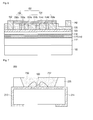
- FIG. 1 is a top view showing a light emitting device 100
- FIG. 2A is a first sectional view taken along line I-I' of the light emitting device 100 according to a first embodiment
- FIG. 3 is a sectional view taken along line II-II' of the light emitting device according to the second embodiment.
- the light emitting device 100 may include a substrate 105, a first conductive semiconductor layer 112 on the substrate 105, an active layer 114 on the first conductive semiconductor layer 112, and a second conductive semiconductor layer 116 on the active layer 114.
- the light emitting device 100 may include an ohmic layer 120 on the second conductive semiconductor layer 116, an insulating layer 130 on the ohmic layer 120, a first branch electrode 140 electrically connected with the first conductive semiconductor layer 112, and a first pad electrode 142 connected with the first branch electrode 140 so that the first pad electrode 142 is electrically connected with the first conductive semiconductor layer 112.
- the light emitting device 100 may include a second pad electrode 152 passing through the insulating layer 130 to make contact with the ohmic layer 120, a second branch electrode 150 connected with the second pad electrode 152 and provided on the insulating layer 130, and a second through electrode 154 passing through the insulating layer 130 to connect the second branch electrode 150 with the ohmic layer 120.
- the embodiment is applicable to a lateral type light emitting device, the embodiment is not limited thereto.
- the substrate 105 may include an insulating substrate or a conductive substrate.
- the substrate 105 may include at least one of sapphire (Al2O3), SiC, Si, GaAs, GaN, ZnO, GaP, InP, Ge, and Ga2O3, or the combination thereof, but the embodiment is not limited thereto.
- a predetermined concave-convex structure (not shown) is formed on the substrate 105 to improve external light extraction efficiency, but the embodiment is not limited thereto.
- a predetermined buffer layer (not shown) is formed on the substrate 105 to reduce lattice mismatch between a light emitting structure 110 and the substrate 105.
- the buffer layer may include at least one of GaN, InN, AIN, InGaN, AlGaN, InAlGaN, and AlInN, but the embodiment is not limited thereto.
- the light emitting device 100 may include the light emitting structure 110 on the substrate 105 or the buffer layer.
- the light emitting structure 110 may include the first conductive semiconductor layer 112 on the substrate 105, the active layer 114 on the first conductive semiconductor layer 112, and the second conductive semiconductor layer 116 on the active layer 114.
- the first conductive semiconductor layer 112 may be realized using a group III-V compound semiconductor doped with first conductive dopants.
- first conductive dopants may include Si, Ge, Sn, Se, and Te serving as N type dopants, but the embodiment is not limited thereto.
- the first conductive semiconductor 112 may include a semiconductor material having a composition formula of InxAlyGa1-x-yN (0 ⁇ x ⁇ 1, 0 ⁇ y ⁇ 1, 0 ⁇ x+y ⁇ 1).
- the first conductive semiconductor layer 112 may include at least one of GaN, InN, AIN, InGaN, AlGaN, InAlGaN, AlInN, AlGaAs, InGaAs, AlInGaAs, GaP, AlGaP, InGaP, AlInGaP, and InP.
- the active layer 114 electrons injected through the first conductive semiconductor layer 112 and holes injected through the second conductive semiconductor layer 116 thereafter meet each other, so that light having energy determined by the inherent energy band of a material constituting the active layer (light emission layer) is emitted.
- the active layer 114 may include at least one of a single quantum well, a multi-quantum well (MQW), a quantum-wire structure, and a quantum dot structure.
- MQW multi-quantum well
- quantum-wire structure a quantum-wire structure
- quantum dot structure a quantum dot structure
- a well layer/barrier layer of the active layer 114 may be formed in a pair structure having at least one of InGaN/GaN, InGaN/InGaN, GaN/AlGaN, InAlGaN/GaN, GaAs(InGaAs),/AlGaAs, and GaP(InGaP)/AlGaP, but the embodiment is not limited thereto.
- the well layer may include a material having a bandgap lower than that of the barrier layer.
- an electron blocking layer is formed on the active layer 114 to perform an electron blocking function and an MQW cladding function of the active layer 114, so that the light emission efficiency can be improved.
- the electron blocking layer may include a semiconductor based on AlxInyGa(1-x-y)N (0 ⁇ x ⁇ 1, 0 ⁇ y ⁇ 1), and may have the energy bandgap higher than that of the active layer 114.
- the electron blocking layer is implanted with P type ions to effectively block overflowed electrons, so that hole injection efficiency can be increased.
- the second conductive semiconductor layer 116 may include a group III-V compound semiconductor layer doped with second conductive dopants.
- the second conductive semiconductor layer 116 may include a semiconductor material having a composition formula of InxAlyGa1-x-yN (0 ⁇ x ⁇ 1, 0 ⁇ y ⁇ 1, 0 ⁇ x+y ⁇ 1).
- the second conductive dopant may include Mg, Zn, Ca, Sr, or Ba serving as the second conductive dopant.
- the light emitting device 100 may include the ohmic layer 120 on the first conductive semiconductor layer 112, the insulating layer 130 on the ohmic layer 120, the first branch electrode 140 electrically connected with the first conductive semiconductor layer 112, and the first pad electrode 142 connected with the first branch electrode 140 so that the first pad electrode 142 is electrically connected with the first conductive semiconductor layer 112.
- the ohmic layer 120 may be formed by stacking single metal, a metal alloy, and a metallic oxide in a multiple structure so that carriers can be efficiently implanted.
- the ohmic layer 120 includes a transmissive electrode to improve light emission efficiency and to lower operating voltage, so that reliability can be improved.
- the ohmic layer 120 may include at least one of ITO (indium tin oxide), IZO (indium zinc oxide), IZTO (indium zinc tin oxide), IAZO (indium aluminum zinc oxide), IGZO (indium gallium zinc oxide), IGTO (indium gallium tin oxide), AZO (aluminum zinc oxide), ATO (antimony tin oxide), GZO (gallium zinc oxide), IZON (IZO Nitride), AGZO (Al-Ga ZnO), IGZO (In-Ga ZnO), ZnO, IrOx, RuOx, NiO, RuOx/ITO, Ni/IrOx/Au, Ni/IrOx/Au/ITO, Ag, Ni, Cr, Ti, Al, Rh, Pd, Ir, Ru, Mg, Zn, Pt, Au, and Hf, or the combination thereof, but the embodiment is not limited thereto.
- ITO indium tin oxide
- the insulating layer 130 may include an electrical insulator including an oxide or a nitride, but the embodiment is not limited thereto.
- the insulating layer 130 includes a transmissive insulating material to increase the light emission efficiency.
- the active layer 114 is not mesa-etched at the position in which the first pad electrode 142 is formed, thereby ensuring an active layer region to improve internal light emission efficiency, and to improve light efficiency due to current spreading.
- the first pad electrode 142 is provided on the insulating layer 130, so that the first pad electrode 142 may be connected with the first branch electrode 140.
- the first pad electrode 142 may be vertically overlapped with the insulating layer 130 and the ohmic layer 120.
- the ohmic layer 120 is provided under the first pad electrode 142 while interposing the insulating layer 130 between the ohmic layer 120 and the first pad electrode 142, thereby widening a light emission area to improve carrier injection efficiency, so that light efficiency can be increased.
- the first branch electrode 140 may be connected with the first conductive semiconductor layer 112 exposed by partially removing the ohmic layer 120, the second conductive semiconductor layer 116, and the active layer 114 through the mesa-etching process.
- the insulating layer 130 is interposed between the light emitting structure exposed through the etching process and the first branch electrode 140 to prevent electrical short.
- an N type branch electrode structure sufficiently ensures a contact area with an N type semiconductor layer to prevent the increase of the operating voltage so that the reliability of the device can be improved.
- the P type branch electrode employs a point contact structure to contribute to current spreading.
- the second conductive semiconductor layer 116 makes contact with the ohmic layer 120 to prevent the increase of the operating voltage, so that the reliability and the light emission efficiency of the device can be maximized.
- the intensity of light (Po) and a wall-plug efficiency ( ⁇ WPE) may be meaningfully increased as shown following table 1.
- Table 1 Items P-contact relative ratio N-contact relative ratio Active area relative ratio Intensity of light (Po) ⁇ WPE Comparative example 100% 100% 100% 96.96 100.00% Embodiment example 25.6% 43.9% 102.2% 98.44 101.35%
- the first branch electrode 140 may include a first ohmic branch electrode 144 making contact with the first conductive semiconductor layer 112 and a first reflective branch electrode 146 provided on the first ohmic branch electrode 144.
- the branch electrode making contact with the first conductive semiconductor layer 112 employs the first ohmic branch electrode 144 to ensure the ohmic characteristic with the first conductive semiconductor layer 112 as much as possible to reduce the operating voltage, so that the electrical reliability can be increased.
- the first ohmic branch electrode 144 may include at least one of Cr, Ni, Ti, Rh, Pd, Ir, Ru, Pt, Au, and Hf, or the combination thereof, but the embodiment is not limited thereto.
- the first reflective branch electrode 146 is provided at an upper portion of the first ohmic branch electrode 144 which does not make contact with the first conductive semiconductor layer 112 to minimize light absorption by the branch electrode, so that external light extraction efficiency may be increased.
- the first reflective branch electrode 146 may include a plurality of layers.
- the first reflective branch electrode 146 may include a lower first reflective branch electrode 146a and an upper first reflective branch electrode 146b, but the embodiment is not limited thereto.
- the first reflective branch electrode 146 may include at least one of Ag, Al, Ni, Ti, Rh, Pd, Ir, Ru, Mg, Zn, Pt, Au, and Hf, or the combination thereof, but the embodiment is not limited thereto.
- the first reflective branch electrode 146 may include Al/Ni or Ag/Ni. If the first reflective branch electrode 146 is formed of one layer, the first reflective branch electrode 146 may include a distributed bragg reflector (DBR), but the embodiment is not limited thereto.
- DBR distributed bragg reflector
- FIG. 2B is a sectional view showing a light emitting device according to another embodiment.
- the first branch electrode 140 may include a first through electrode 145 making contact with the first conductive semiconductor layer 112 and a first reflective branch electrode 146 provided on the first through electrode 145.
- the first through electrode 145 of the first branch electrode making contact with the first conductive semiconductor layer 112 employs an ohmic material, thereby ensuring an ohmic characteristic with the first conductive semiconductor layer 112 as much as possible to reduce operating voltage, so that the electrical reliability can be increased.
- the first reflective branch electrode 146 may include a plurality of layers.
- the first reflective branch electrode 146 may include the lower first reflective branch electrode 146a and the upper first reflective branch electrode 146b, but the embodiment is not limited thereto.
- the first branch electrode 140 may include the first through electrode 145 making contact with the first conductive semiconductor layer 112.
- the contact ratio between the first through electrode 145 and the first conductive semiconductor layer 112 may be in the range of about 17% to about 44%.
- the contact ratio between the first through electrode 145 and the first conductive semiconductor layer 112 may be in the range of about 17% to about 44%.
- the first through electrode 145 may have one bar structure instead of the point contact structure in the branch electrode shown in FIG. 1 .
- the first pad electrode 142 is provided on the insulating layer 130 so that the first pad electrode 142 may not make contact with the first conductive semiconductor layer 112.
- the intensity of light (Po) and a wall-plug efficiency ( ⁇ WPE) are meaningfully increased due to the systematical coupling with the p-point contact structure.
- the first through electrode 145 employs a point contact structure.
- One N type branch electrode may have a two-bar structure.
- the first pad electrode 142 is provided on the insulating layer 130, so that the first pad electrode 142 may not make contact with the first conductive semiconductor layer 112.
- FIG. 2B shows the first through electrode 145 having a three-bar structure in one N type branch electrode, in relation to the point contact structure of the first through electrode 145.
- the intensity of light (Po) and the wall-plug efficiency ( ⁇ WPE) are meaningfully increased due to the systematical coupling with the p-point contact structure.
- the first through electrode 145 employs a point contact structure, and a four-bar structure may be provided in one N type branch electrode.
- the first pad electrode 142 is provided on the insulating layer 130, so that the first pad electrode 142 may not make contact with the first conductive semiconductor layer 112.
- the intensity of light (Po) and the wall-plug efficiency ( ⁇ WPE) are meaningfully increased due to the systematical coupling with the p-point contact structure.
- the first through electrode 145 employs a point contact structure, and a five-bar structure may be provided in one N type branch electrode.
- the first pad electrode 142 is provided on the insulating layer 130, so that the first pad electrode 142 may not make contact with the first conductive semiconductor layer 112.
- the intensity of light (Po) and the wall-plug efficiency ( ⁇ WPE) are meaningfully increased due to the systematical coupling with the p-point contact structure.
- the contact ratio between the second through electrode 154 and the ohmic layer 120 may be in the range of about 25% to about 34%, but the embodiment is not limited thereto.
- the light emitting device may include a second pad electrode 152 passing through the insulating layer 130 to make contact with the ohmic layer 120, a second branch electrode 150 connected with the second pad electrode 152 and provided on the insulating layer 130, and a second through electrode 154 passing through the insulating layer 130 to connect the second branch electrode 150 with the ohmic layer 120.
- the through electrode is shown as a component of the branch electrode, the embodiment is not limited thereto.
- the second through electrode 154 may be a second ohmic through electrode, and the second branch electrode 150 may be a second reflective branch electrode 156.
- the second through electrode 154 may include at least one of Cr, Ni, Ti, Rh, Pd, Ir, Ru, Pt, Au, and Hf or the combination thereof, but the embodiment is not limited thereto.
- the second reflective branch electrode 156 may include a plurality of layers.
- the second reflective branch electrode 156 may include the lower second reflective branch electrode 156a and the upper second reflective branch electrode 156b, but the embodiment is not limited thereto.
- the second reflective branch electrode 156 may include at least one of Ag, Al, Ni, Ti, Rh, Pd, Ir, Ru, Mg, Zn, Pt, Au, and Hf or the combination thereof, but the embodiment is not limited thereto.
- the second reflective branch electrode 156 may include Al/Ni or Ag/Ni. If the second reflective branch electrode 156 is formed at one layer, the second reflective branch electrode 156 may include a distributed bragg reflector (DBR), but the embodiment is not limited thereto.
- DBR distributed bragg reflector
- a current spreading layer 160 is provided on the second conductive semiconductor layer 116 so that the current spreading layer 160 is overlapped with the second pad electrode 152, thereby increasing current spreading, so that the whole light emission efficiency can be increased.
- the current spreading layer 160 may include a non-conductive region, a first conductive type ion implantation layer, an insulating material, or an amorphous region, but the embodiment is not limited thereto.
- FIG. 4 is a sectional view showing a light emitting device according to the second embodiment.
- the second embodiment may employ the technical features of the first embodiment.
- the second branch electrode 150 may include the second reflective branch electrode 156 and a third reflective through electrode 158.
- the third reflective through electrode 158 may include a plurality of layers.
- the third reflective through electrode 158 may include an outer third reflective through electrode 158a and an inner third reflective through electrode 158b, but the embodiment is not limited thereto.
- the third through electrode includes a reflective electrode material to minimize the light absorption by the branch electrode, and the ohmic layer 120 makes contact with the light emitting structure to ensure the ohmic characteristic so that the reliability can be maintained and the external light extraction efficiency can be maximized.
- FIG. 5 is a sectional view showing a light emitting device according to a third embodiment.
- the third embodiment may employ the technical features of the first embodiment or the second embodiment.
- a plurality of second through electrodes 154 may be provided.
- the second through electrodes 154 may have mutually different contact areas with the ohmic layer 120. Accordingly, at least two second through electrodes 154 may have mutually different contact areas with the ohmic contact layer 120.
- the contact area of the second through electrode 154 with the ohmic layer 120 is increased as the second through electrode 154 is farther away from the second pad electrode 152 to contribute to the current spreading, so that the light emission efficiency can be increased.
- the second through electrode 154 includes second through electrodes 154a, 154b, 154c, 154d, and 154e having contact areas with the ohmic layer 120, which are increased as the second through electrode 154 is farther away from the second pad electrode 152, to contribute to the current spreading, so that the light emission efficiency can be increased.
- the contact area of the second through electrode 154 with the ohmic layer 120 may be decreased as the second through electrode 154 is farther away from the second pad electrode 152.
- the contact area of the second through electrode 154 with the ohmic layer 120 may be randomly varied as the second through electrode 154 is farther away from the second pad electrode 152.
- a horizontal width of a contact region of the second through electrodes 154a, 154b, 154c, 154d, and 154e with the ohmic layer 120 may be in the range of about 20 ⁇ m to about 60 ⁇ m, but the embodiment is not limited thereto.
- the contact area of the second through electrode 154a, which is closest to the second pad electrode 152, with the ohmic layer 120 has a first horizontal width ranging from about 1/2 to about 1/4 of a second horizontal width of the contact area of the second through electrode 154e, which is most widely spaced apart from the second pad electrode 152, with the ohmic layer 120.
- the contact area of the second through electrode 154a, which is closest to the second pad electrode 152, with the ohmic layer 120 has the first horizontal width corresponding to about 1/3 of the second horizontal width of the contact area of the second through electrode 154e, which is most widely spaced apart from the second pad electrode 152, with the ohmic layer 120.
- the contact area of the second through electrode 154a, which is closest to the second pad electrode 152, with the ohmic layer 120 has a horizontal width of about 20 ⁇ m.
- the second horizontal width of the contact area of the second through electrode 154e, which is most widely spaced apart from the second pad electrode 152, with the ohmic layer 120 may be about 60 ⁇ m.
- the contact area of the second through electrode 154 with the ohmic layer 120 is varied as the second through electrode 154 is farther away from the second pad electrode 152, the through electrodes 154a, 154b, 154c, 154d, and 154e are arranged at a uniform interval to contribute to the uniform current spreading.
- the shape of the second through electrode 154 to make contact with the ohmic layer 120 may be various shapes including a polygonal shape such as a bar shape, a square shape, or a rectangular shape, a circular shape, or an oval shape.
- the vertical sectional shape of the second through electrode 154 may be a rectangular shape, the embodiment is not limited thereto.
- the second through electrode 154 may have an upper width wider than a lower width, that is, a width narrowed to the lower portion.
- the second through electrode 154 may have the upper width narrower than the lower width, that is, a width widened to the lower portion.
- a horizontal sectional width of the second through electrode 154 is equal to the horizontal sectional width of the second reflective branch electrode 156, the embodiment is not limited thereto.
- the horizontal sectional width of the second through electrode 154 may be greater than or less than the horizontal sectional width of the second reflective branch electrode 156.
- FIG. 6 is a sectional view showing a light emitting device according to a fourth embodiment.
- the fourth embodiment may employ the technical features of the first embodiment to the third embodiment.
- a region of the ohmic layer 120 which is vertically overlapped with the second pad electrode 152, may make contact with the second conductive semiconductor layer 116.
- a current spreading layer is not provided on the second conductive semiconductor layer 116 overlapped with the second pad electrode 152, so that the ohmic layer 120 may make contact with the second conductive semiconductor layer 116.
- the light emission characteristic can be maintained or enhanced, thereby more improving the problem related to the increase of the operating voltage, which is a disadvantage of a point contact, as compared with the related art.
- the embodiment can provide a light emitting device capable of improving reliability by contributing to the increase in the current spreading and the decrease in the operating voltage as the second conductive semiconductor layer makes contact with the ohmic layer, and the ohmic layer makes contact with the through electrode, a method of fabricating the same, a light emitting device package, and a lighting system.
- a portion of the branch electrode making contact with the semiconductor layer is formed of a material representing a superior ohmic characteristic, and a remaining portion of the branch electrode includes a material representing superior reflectivity, so that the reliability can be maintained, and the light extraction efficiency can be maximized.
- the contact between the lower end of the pad electrode and the semiconductor layer is controlled, so that the whole light emission efficiency of a chip can be improved due to the current spreading, thereby improving the light efficiency.
- the light emitting device is applicable to a display apparatus such as a portable terminal and a laptop computer, or variously applicable to a lighting device and an indication device.
- the light emitting device is applicable to a lamp of a vehicle, a streetlamp, an electric board, and a headlamp .
- FIG. 7 is a sectional view showing a light emitting device package in which the light emitting device according to the embodiments is mounted.
- the light emitting device package may include a package body part 205, third and fourth electrode layers 213 and 214 mounted on the package body part 205, a light emitting device 100 mounted on the package body part 205 and electrically connected with the third and fourth electrode layers 213 and 214, and a molding member 230 to surround the light emitting device 100.
- the third and fourth electrode layers 213 and 214 are electrically isolated from each other to supply power to the light emitting device 100.
- the third and fourth electrode layers 213 and 214 reflect light emitted from the light emitting device 100 to increase light efficiency, and discharge heat emitted from the light emitting device 100 to the outside.
- the light emitting device 100 may be electrically connected with the third electrode layer 213 and/or the fourth electrode layer 214 through one of a wire scheme, a flip-chip scheme, or a die-bonding scheme.
- FIG. 8 is an exploded perspective view showing a lighting system according to the embodiment.
- the lighting system according to the embodiment may include a cover 2100, a light source module 2200, a radiator 2400, a power supply part 2600, an inner case 2700, and a socket 2800.
- the lighting system according to the embodiment may further include at least one of a member 2300 and a holder 2500.
- the light source module 2200 may include the light emitting device 100 or the light emitting device module 200 according to the embodiment.
- the light source module 2200 may include a light source part 2210, a connection plate 2230, and a connector 2250.
- the member 2300 is provided at a top surface of the radiator 2400, and includes guide grooves 2310 into which a plurality of light sources 2210 and the connector 2250 are inserted.
- the holder 2500 covers a receiving groove 2719 of an insulating part 2710 of the inner case 2700. Accordingly, the power supply part 2600 received in the receiving groove of the inner case 2700 is closed inside the inner case 2700 by the holder 2500.
- the holder 2500 has a guide protrusion part 2510.
- the power supply part 2600 may include a protrusion 2610, a guide part 2630, a base 2650, and an extension part 2670.
- the inner case 2700 may include a molding part therein together with the power supply part 2600.
- the molding part is prepared by hardening molding liquid, and the power supply part 2600 may be fixed inside the inner case 2700 by the molding part.
- a light emitting device capable of improving reliability, a method of fabricating the same, a light emitting device package, and a lighting system.
- the embodiments provide a light emitting device capable of improving light extraction efficiency, a method of fabricating the same, a light emitting device package, and a lighting system.
- a light emitting device which may include a substrate, a first conductive semiconductor layer on the substrate, an active layer on the first conductive semiconductor layer, and a second conductive semiconductor layer on the active layer.
- the light emitting device may include an ohmic layer on the second conductive semiconductor layer, an insulating layer on the ohmic layer, a first branch electrode electrically connected with the first conductive semiconductor layer, and a first pad electrode connected with the first branch electrode such that the first pad electrode is electrically connected with the first conductive semiconductor layer.
- the light emitting device may include a second pad electrode passing through the insulating layer to make contact with the ohmic layer, a second branch electrode connected with the second pad electrode and provided on the insulating layer, and a second through electrode passing through the insulating layer to connect the second branch electrode with the ohmic layer.
- a light emitting device which may include a substrate, a first conductive semiconductor layer on the substrate, an active layer on the first conductive semiconductor layer, a second conductive semiconductor layer on the active layer, an ohmic layer on the second conductive semiconductor layer, an insulating layer on the ohmic layer, a first electrode pad on the insulating layer, a first branch electrode extending from the first electrode pad and provided on the first conductive semiconductor layer, a second electrode pad passing through the insulating layer to make contact with the ohmic layer, and a second branch electrode to electrically connect the second electrode pad with the second conductive semiconductor layer.
- the second branch electrode may include a second reflective branch electrode extending from the second electrode pad and provided on the insulating layer and at least one second through electrode passing through the insulating layer to connect the second reflective branch electrode with the ohmic layer.
- a light emitting device capable of improving reliability by contributing to the increase in the current spreading and the decrease in the operating voltage as the second conductive semiconductor layer makes contact with the ohmic layer and the ohmic layer makes contact with the through electrode, a method of fabricating the same, a light emitting device package, and a lighting system can be provided.
- a portion of the branch electrode making contact with the semiconductor layer may be formed of a material representing a superior ohmic characteristic, and a remaining portion of the branch electrode may include a material representing superior reflectivity, so that the reliability can be maintained, and the light extraction efficiency can be maximized.
- the contact between the lower end of the pad electrode and the semiconductor layer may be controlled, so that the whole light emission efficiency of a chip can be improved due to the current spreading, thereby improving the light efficiency.
- any reference in this specification to "one embodiment,” “an embodiment,” “example embodiment,” etc. means that a particular feature, structure, or characteristic described in connection with the embodiment is included in at least one embodiment of the invention.
- the appearances of such phrases in various places in the specification are not necessarily all referring to the same embodiment.
Landscapes
- Led Devices (AREA)
- Led Device Packages (AREA)
Abstract
Description
- The embodiment relates to a light emitting device, a method of fabricating the same, a light emitting device package, and a lighting system.
- Generally, a light emitting device (LED) includes a p-n junction diode having a characteristic of converting electric energy into light energy. The p-n junction diode can be formed by combining group III-V compound semiconductors on the periodic table. The light emitting device can represent various colors by adjusting the compositional ratio of the compound semiconductors.
- When a forward voltage is applied to an LED, electrons at an n layer are combined with holes at a p layer, so that energy corresponding to an energy gap between a conduction band and a valance band may be emitted. This energy is mainly emitted in the form of heat or light. The LED emits the energy in the form of light.
- For instance, a nitride semiconductor has been spotlighted in the development field of optical devices and high-power electronic devices due to superior thermal stability and wide band gap energy thereof. In particular, blue, green, and UV light emitting devices employing the nitride semiconductor have already been commercialized and extensively used.
- A lateral-type light emitting device among light emitting devices according to the related art is formed in a structure in which a nitride semiconductor layer is formed on a substrate, and two electrode layers are arranged on the nitride semiconductor layer.
- Meanwhile, the lateral-type light emitting device according to the related art has a big loss caused at the active layer since mesa etching is performed with respect to a wide area. Accordingly, in order to compensate for the loss, various attempts are performed to ensure a wider active layer.
- For example, according to the related art, an attempt to ensure a wider active layer is performed based on the electrical connection with the nitride semiconductor layer via a through electrode serving as a portion of an electrode layer. However, the related art has a problem in reliability since operating voltage VF is increased, and the improvement of the problem is required.
- In addition, according to the related art, the light extraction efficiency may be degraded due to the light absorption of the electrode layer.
- The embodiments will be described in detail with reference to the following drawings in which like reference numerals refer to like elements wherein:
-
FIG. 1 is a top view showing a light emitting device according to the embodiment; -
FIG. 2A is a first sectional view showing a light emitting device according to a first embodiment; -
FIG. 2B is a sectional view showing a light emitting device according to another embodiment; -
FIG. 3 is a second sectional view showing a light emitting device according to the first embodiment; -
FIG. 4 is a second sectional view showing a light emitting device according to a second embodiment; -
FIG. 5 is a second sectional view showing a light emitting device according to a third embodiment; -
FIG. 6 is a second sectional view showing a light emitting device according to a fourth embodiment; -
FIG. 7 is a sectional view showing a light emitting device package according to the embodiment; and -
FIG. 8 is a perspective view showing a lighting system according to the embodiment. - Hereinafter, a light emitting device, a light emitting device package, and a lighting system according to the embodiment will be described with reference to accompanying drawings. As broadly described and embodied herein, provided are a light emitting device capable of improving reliability, a method of fabricating the same, a light emitting device package, and a lighting system. The light emitting device as disclosed herein provides improved light extraction efficiency, among other advantages.
- In the description of embodiments, it will be understood that when a layer (or film) is referred to as being 'on' another layer or substrate, it can be directly on another layer or substrate, or intervening layers may also be present. Further, it will be understood that when a layer is referred to as being 'under' another layer, it can be directly under another layer, and one or more intervening layers may also be present. In addition, it will also be understood that when a layer is referred to as being 'between' two layers, it can be the only layer between the two layers, or one or more intervening layers may also be present.
-
FIG. 1 is a top view showing alight emitting device 100,FIG. 2A is a first sectional view taken along line I-I' of thelight emitting device 100 according to a first embodiment, andFIG. 3 is a sectional view taken along line II-II' of the light emitting device according to the second embodiment. - The
light emitting device 100 according to the embodiment may include asubstrate 105, a firstconductive semiconductor layer 112 on thesubstrate 105, anactive layer 114 on the firstconductive semiconductor layer 112, and a secondconductive semiconductor layer 116 on theactive layer 114. - In addition, according to the embodiment, the
light emitting device 100 may include anohmic layer 120 on the secondconductive semiconductor layer 116, aninsulating layer 130 on theohmic layer 120, afirst branch electrode 140 electrically connected with the firstconductive semiconductor layer 112, and afirst pad electrode 142 connected with thefirst branch electrode 140 so that thefirst pad electrode 142 is electrically connected with the firstconductive semiconductor layer 112. - In addition, according to the embodiment, the
light emitting device 100 may include asecond pad electrode 152 passing through theinsulating layer 130 to make contact with theohmic layer 120, asecond branch electrode 150 connected with thesecond pad electrode 152 and provided on theinsulating layer 130, and a second throughelectrode 154 passing through theinsulating layer 130 to connect thesecond branch electrode 150 with theohmic layer 120. - Although the embodiment is applicable to a lateral type light emitting device, the embodiment is not limited thereto.
- Hereinafter, features of the light emitting device according to the embodiment will be described with reference to
FIGS. 1, 2A , and3 . - According to the embodiment, the
substrate 105 may include an insulating substrate or a conductive substrate. For example, thesubstrate 105 may include at least one of sapphire (Al2O3), SiC, Si, GaAs, GaN, ZnO, GaP, InP, Ge, and Ga2O3, or the combination thereof, but the embodiment is not limited thereto. A predetermined concave-convex structure (not shown) is formed on thesubstrate 105 to improve external light extraction efficiency, but the embodiment is not limited thereto. - According to the embodiment, a predetermined buffer layer (not shown) is formed on the
substrate 105 to reduce lattice mismatch between alight emitting structure 110 and thesubstrate 105. The buffer layer may include at least one of GaN, InN, AIN, InGaN, AlGaN, InAlGaN, and AlInN, but the embodiment is not limited thereto. - According to the embodiment, the
light emitting device 100 may include thelight emitting structure 110 on thesubstrate 105 or the buffer layer. Thelight emitting structure 110 may include the firstconductive semiconductor layer 112 on thesubstrate 105, theactive layer 114 on the firstconductive semiconductor layer 112, and the secondconductive semiconductor layer 116 on theactive layer 114. - The first
conductive semiconductor layer 112 may be realized using a group III-V compound semiconductor doped with first conductive dopants. For example, when the firstconductive semiconductor layer 112 is an N type semiconductor layer, the first conductive dopants may include Si, Ge, Sn, Se, and Te serving as N type dopants, but the embodiment is not limited thereto. - The first
conductive semiconductor 112 may include a semiconductor material having a composition formula of InxAlyGa1-x-yN (0≤x≤1, 0≤y≤1, 0≤x+y≤1). - For example, the first
conductive semiconductor layer 112 may include at least one of GaN, InN, AIN, InGaN, AlGaN, InAlGaN, AlInN, AlGaAs, InGaAs, AlInGaAs, GaP, AlGaP, InGaP, AlInGaP, and InP. - In the
active layer 114, electrons injected through the firstconductive semiconductor layer 112 and holes injected through the secondconductive semiconductor layer 116 thereafter meet each other, so that light having energy determined by the inherent energy band of a material constituting the active layer (light emission layer) is emitted. - The
active layer 114 may include at least one of a single quantum well, a multi-quantum well (MQW), a quantum-wire structure, and a quantum dot structure. - A well layer/barrier layer of the
active layer 114 may be formed in a pair structure having at least one of InGaN/GaN, InGaN/InGaN, GaN/AlGaN, InAlGaN/GaN, GaAs(InGaAs),/AlGaAs, and GaP(InGaP)/AlGaP, but the embodiment is not limited thereto. The well layer may include a material having a bandgap lower than that of the barrier layer. - According to the embodiment, an electron blocking layer is formed on the
active layer 114 to perform an electron blocking function and an MQW cladding function of theactive layer 114, so that the light emission efficiency can be improved. - For example, the electron blocking layer may include a semiconductor based on AlxInyGa(1-x-y)N (0≤x≤1, 0≤y≤1), and may have the energy bandgap higher than that of the
active layer 114. - The electron blocking layer is implanted with P type ions to effectively block overflowed electrons, so that hole injection efficiency can be increased.
- According to the embodiment, the second
conductive semiconductor layer 116 may include a group III-V compound semiconductor layer doped with second conductive dopants. For example, the secondconductive semiconductor layer 116 may include a semiconductor material having a composition formula of InxAlyGa1-x-yN (0≤x≤1, 0≤y≤1, 0≤x+y≤1). When the secondconductive semiconductor layer 116 includes a P type semiconductor layer, the second conductive dopant may include Mg, Zn, Ca, Sr, or Ba serving as the second conductive dopant. - As shown in
FIGS. 2A and3 , according to the embodiment, thelight emitting device 100 may include theohmic layer 120 on the firstconductive semiconductor layer 112, the insulatinglayer 130 on theohmic layer 120, thefirst branch electrode 140 electrically connected with the firstconductive semiconductor layer 112, and thefirst pad electrode 142 connected with thefirst branch electrode 140 so that thefirst pad electrode 142 is electrically connected with the firstconductive semiconductor layer 112. - The
ohmic layer 120 may be formed by stacking single metal, a metal alloy, and a metallic oxide in a multiple structure so that carriers can be efficiently implanted. Theohmic layer 120 includes a transmissive electrode to improve light emission efficiency and to lower operating voltage, so that reliability can be improved. - For example, the
ohmic layer 120 may include at least one of ITO (indium tin oxide), IZO (indium zinc oxide), IZTO (indium zinc tin oxide), IAZO (indium aluminum zinc oxide), IGZO (indium gallium zinc oxide), IGTO (indium gallium tin oxide), AZO (aluminum zinc oxide), ATO (antimony tin oxide), GZO (gallium zinc oxide), IZON (IZO Nitride), AGZO (Al-Ga ZnO), IGZO (In-Ga ZnO), ZnO, IrOx, RuOx, NiO, RuOx/ITO, Ni/IrOx/Au, Ni/IrOx/Au/ITO, Ag, Ni, Cr, Ti, Al, Rh, Pd, Ir, Ru, Mg, Zn, Pt, Au, and Hf, or the combination thereof, but the embodiment is not limited thereto. - The insulating
layer 130 may include an electrical insulator including an oxide or a nitride, but the embodiment is not limited thereto. The insulatinglayer 130 includes a transmissive insulating material to increase the light emission efficiency. - According to the embodiment, the
active layer 114 is not mesa-etched at the position in which thefirst pad electrode 142 is formed, thereby ensuring an active layer region to improve internal light emission efficiency, and to improve light efficiency due to current spreading. - Therefore, according to the embodiment, the
first pad electrode 142 is provided on the insulatinglayer 130, so that thefirst pad electrode 142 may be connected with thefirst branch electrode 140. Thefirst pad electrode 142 may be vertically overlapped with the insulatinglayer 130 and theohmic layer 120. Theohmic layer 120 is provided under thefirst pad electrode 142 while interposing the insulatinglayer 130 between theohmic layer 120 and thefirst pad electrode 142, thereby widening a light emission area to improve carrier injection efficiency, so that light efficiency can be increased. - According to the embodiment, as shown in
FIG. 2A , thefirst branch electrode 140 may be connected with the firstconductive semiconductor layer 112 exposed by partially removing theohmic layer 120, the secondconductive semiconductor layer 116, and theactive layer 114 through the mesa-etching process. In this case, the insulatinglayer 130 is interposed between the light emitting structure exposed through the etching process and thefirst branch electrode 140 to prevent electrical short. - According to the embodiment, an N type branch electrode structure sufficiently ensures a contact area with an N type semiconductor layer to prevent the increase of the operating voltage so that the reliability of the device can be improved. The P type branch electrode employs a point contact structure to contribute to current spreading. The second
conductive semiconductor layer 116 makes contact with theohmic layer 120 to prevent the increase of the operating voltage, so that the reliability and the light emission efficiency of the device can be maximized. - For example, as shown in
FIG. 1 , according to the structure of the first embodiment, when the N type branch electrode structure sufficiently ensures the contact area with the N type semiconductor layer and the P type branch electrode employs the point contact structure, the intensity of light (Po) and a wall-plug efficiency (ΔWPE) may be meaningfully increased as shown following table 1.Table 1 Items P-contact relative ratio N-contact relative ratio Active area relative ratio Intensity of light (Po) ΔWPE Comparative example 100% 100% 100% 96.96 100.00% Embodiment example 25.6% 43.9% 102.2% 98.44 101.35% - According to the embodiment, the
first branch electrode 140 may include a firstohmic branch electrode 144 making contact with the firstconductive semiconductor layer 112 and a firstreflective branch electrode 146 provided on the firstohmic branch electrode 144. - According to the embodiment, the branch electrode making contact with the first
conductive semiconductor layer 112 employs the firstohmic branch electrode 144 to ensure the ohmic characteristic with the firstconductive semiconductor layer 112 as much as possible to reduce the operating voltage, so that the electrical reliability can be increased. - For example, the first
ohmic branch electrode 144 may include at least one of Cr, Ni, Ti, Rh, Pd, Ir, Ru, Pt, Au, and Hf, or the combination thereof, but the embodiment is not limited thereto. - In addition, according to the embodiment, the first
reflective branch electrode 146 is provided at an upper portion of the firstohmic branch electrode 144 which does not make contact with the firstconductive semiconductor layer 112 to minimize light absorption by the branch electrode, so that external light extraction efficiency may be increased. - For example, the first
reflective branch electrode 146 may include a plurality of layers. For example, the firstreflective branch electrode 146 may include a lower firstreflective branch electrode 146a and an upper firstreflective branch electrode 146b, but the embodiment is not limited thereto. - The first
reflective branch electrode 146 may include at least one of Ag, Al, Ni, Ti, Rh, Pd, Ir, Ru, Mg, Zn, Pt, Au, and Hf, or the combination thereof, but the embodiment is not limited thereto. - For example, if the first
reflective branch electrode 146 is formed of two layers, the firstreflective branch electrode 146 may include Al/Ni or Ag/Ni. If the firstreflective branch electrode 146 is formed of one layer, the firstreflective branch electrode 146 may include a distributed bragg reflector (DBR), but the embodiment is not limited thereto. -
FIG. 2B is a sectional view showing a light emitting device according to another embodiment. - Differently from
FIG. 2A , a point contact structure may be possible in thefirst branch electrode 140 inFIG. 2B . For example, as shown inFIG. 2B , thefirst branch electrode 140 may include a first throughelectrode 145 making contact with the firstconductive semiconductor layer 112 and a firstreflective branch electrode 146 provided on the first throughelectrode 145. - According to the embodiment, the first through
electrode 145 of the first branch electrode making contact with the firstconductive semiconductor layer 112 employs an ohmic material, thereby ensuring an ohmic characteristic with the firstconductive semiconductor layer 112 as much as possible to reduce operating voltage, so that the electrical reliability can be increased. - The first
reflective branch electrode 146 may include a plurality of layers. For example, the firstreflective branch electrode 146 may include the lower firstreflective branch electrode 146a and the upper firstreflective branch electrode 146b, but the embodiment is not limited thereto. - According to the embodiment, when the point contact structure is employed in the
first branch electrode 140, thefirst branch electrode 140 may include the first throughelectrode 145 making contact with the firstconductive semiconductor layer 112. The contact ratio between the first throughelectrode 145 and the firstconductive semiconductor layer 112 may be in the range of about 17% to about 44%. - For example, detailed embodiments according to the contact ratio between the first through
electrode 145 and the firstconductive semiconductor layer 112 are shown in Table 2, and have the meaning increase in the intensity of light (Po) and a wall-plug efficiency (ΔWPE) as compared with a comparative example.Table 2 Items P-contact relative ratio N-contact relative ratio Active area relative ratio Intensity of light (Po) ΔWPE Comparative example 97.9% 99.4% 100% 96.77 100% Embodiment A 25.6% 43.9% 102.2% 98.44 101.35% Embodiment B 25.6% 32.1 % 103.3% 98.72 101.35% Embodiment C 25.6% 21.9% 104.4% 98.46 101.15% Embodiment D 25.6% 17.4% 104.3% 98.78 101.15% - According to the embodiments, the contact ratio between the first through
electrode 145 and the firstconductive semiconductor layer 112 may be in the range of about 17% to about 44%. - For example, according to embodiment A, the first through
electrode 145 may have one bar structure instead of the point contact structure in the branch electrode shown inFIG. 1 . Thefirst pad electrode 142 is provided on the insulatinglayer 130 so that thefirst pad electrode 142 may not make contact with the firstconductive semiconductor layer 112. According to embodiment A, the intensity of light (Po) and a wall-plug efficiency (ΔWPE) are meaningfully increased due to the systematical coupling with the p-point contact structure. - In addition, according to embodiment B, the first through
electrode 145 employs a point contact structure. One N type branch electrode may have a two-bar structure. Thefirst pad electrode 142 is provided on the insulatinglayer 130, so that thefirst pad electrode 142 may not make contact with the firstconductive semiconductor layer 112.FIG. 2B shows the first throughelectrode 145 having a three-bar structure in one N type branch electrode, in relation to the point contact structure of the first throughelectrode 145. - In even embodiment B, the intensity of light (Po) and the wall-plug efficiency (ΔWPE) are meaningfully increased due to the systematical coupling with the p-point contact structure.
- In addition, according to embodiment C, the first through
electrode 145 employs a point contact structure, and a four-bar structure may be provided in one N type branch electrode. Thefirst pad electrode 142 is provided on the insulatinglayer 130, so that thefirst pad electrode 142 may not make contact with the firstconductive semiconductor layer 112. In even embodiment C, the intensity of light (Po) and the wall-plug efficiency (ΔWPE) are meaningfully increased due to the systematical coupling with the p-point contact structure. - In addition, according to embodiment D, the first through
electrode 145 employs a point contact structure, and a five-bar structure may be provided in one N type branch electrode. Thefirst pad electrode 142 is provided on the insulatinglayer 130, so that thefirst pad electrode 142 may not make contact with the firstconductive semiconductor layer 112. In even embodiment D, the intensity of light (Po) and the wall-plug efficiency (ΔWPE) are meaningfully increased due to the systematical coupling with the p-point contact structure. - According to the embodiment, the contact ratio between the second through
electrode 154 and theohmic layer 120 may be in the range of about 25% to about 34%, but the embodiment is not limited thereto. - As shown in
FIG. 3 , according to the embedment, the light emitting device may include asecond pad electrode 152 passing through the insulatinglayer 130 to make contact with theohmic layer 120, asecond branch electrode 150 connected with thesecond pad electrode 152 and provided on the insulatinglayer 130, and a second throughelectrode 154 passing through the insulatinglayer 130 to connect thesecond branch electrode 150 with theohmic layer 120. - According to the embodiment, although the through electrode is shown as a component of the branch electrode, the embodiment is not limited thereto.
- The second through
electrode 154 may be a second ohmic through electrode, and thesecond branch electrode 150 may be a secondreflective branch electrode 156. - For example, the second through
electrode 154 may include at least one of Cr, Ni, Ti, Rh, Pd, Ir, Ru, Pt, Au, and Hf or the combination thereof, but the embodiment is not limited thereto. - For example, the second
reflective branch electrode 156 may include a plurality of layers. For example, the secondreflective branch electrode 156 may include the lower secondreflective branch electrode 156a and the upper secondreflective branch electrode 156b, but the embodiment is not limited thereto. - The second
reflective branch electrode 156 may include at least one of Ag, Al, Ni, Ti, Rh, Pd, Ir, Ru, Mg, Zn, Pt, Au, and Hf or the combination thereof, but the embodiment is not limited thereto. - For example, if the second
reflective branch electrode 156 is formed at two layers, the secondreflective branch electrode 156 may include Al/Ni or Ag/Ni. If the secondreflective branch electrode 156 is formed at one layer, the secondreflective branch electrode 156 may include a distributed bragg reflector (DBR), but the embodiment is not limited thereto. - According to the embodiment, a current spreading
layer 160 is provided on the secondconductive semiconductor layer 116 so that the current spreadinglayer 160 is overlapped with thesecond pad electrode 152, thereby increasing current spreading, so that the whole light emission efficiency can be increased. - For example, the current spreading
layer 160 may include a non-conductive region, a first conductive type ion implantation layer, an insulating material, or an amorphous region, but the embodiment is not limited thereto. -
FIG. 4 is a sectional view showing a light emitting device according to the second embodiment. - The second embodiment may employ the technical features of the first embodiment.
- According to the second embodiment, the
second branch electrode 150 may include the secondreflective branch electrode 156 and a third reflective throughelectrode 158. - The third reflective through
electrode 158 may include a plurality of layers. For example, the third reflective throughelectrode 158 may include an outer third reflective throughelectrode 158a and an inner third reflective throughelectrode 158b, but the embodiment is not limited thereto. - According to the second embodiment, the third through electrode includes a reflective electrode material to minimize the light absorption by the branch electrode, and the
ohmic layer 120 makes contact with the light emitting structure to ensure the ohmic characteristic so that the reliability can be maintained and the external light extraction efficiency can be maximized. -
FIG. 5 is a sectional view showing a light emitting device according to a third embodiment. - The third embodiment may employ the technical features of the first embodiment or the second embodiment.
- According to the third embodiment, a plurality of second through
electrodes 154 may be provided. The second throughelectrodes 154 may have mutually different contact areas with theohmic layer 120. Accordingly, at least two second throughelectrodes 154 may have mutually different contact areas with theohmic contact layer 120. - For example, the contact area of the second through
electrode 154 with theohmic layer 120 is increased as the second throughelectrode 154 is farther away from thesecond pad electrode 152 to contribute to the current spreading, so that the light emission efficiency can be increased. - For example, the second through
electrode 154 includes second throughelectrodes ohmic layer 120, which are increased as the second throughelectrode 154 is farther away from thesecond pad electrode 152, to contribute to the current spreading, so that the light emission efficiency can be increased. - Meanwhile, the contact area of the second through
electrode 154 with theohmic layer 120 may be decreased as the second throughelectrode 154 is farther away from thesecond pad electrode 152. - In addition, the contact area of the second through
electrode 154 with theohmic layer 120 may be randomly varied as the second throughelectrode 154 is farther away from thesecond pad electrode 152. - According to the embodiment, a horizontal width of a contact region of the second through
electrodes ohmic layer 120 may be in the range of about 20 µm to about 60 µm, but the embodiment is not limited thereto. - According to the embodiment, the contact area of the second through
electrode 154a, which is closest to thesecond pad electrode 152, with theohmic layer 120 has a first horizontal width ranging from about 1/2 to about 1/4 of a second horizontal width of the contact area of the second throughelectrode 154e, which is most widely spaced apart from thesecond pad electrode 152, with theohmic layer 120. - For example, according to the embodiment, the contact area of the second through
electrode 154a, which is closest to thesecond pad electrode 152, with theohmic layer 120 has the first horizontal width corresponding to about 1/3 of the second horizontal width of the contact area of the second throughelectrode 154e, which is most widely spaced apart from thesecond pad electrode 152, with theohmic layer 120. - For example, the contact area of the second through
electrode 154a, which is closest to thesecond pad electrode 152, with theohmic layer 120 has a horizontal width of about 20 µm. The second horizontal width of the contact area of the second throughelectrode 154e, which is most widely spaced apart from thesecond pad electrode 152, with theohmic layer 120 may be about 60 µm. - According to the embodiment, although the contact area of the second through
electrode 154 with theohmic layer 120 is varied as the second throughelectrode 154 is farther away from thesecond pad electrode 152, the throughelectrodes - According to the embodiment, the shape of the second through
electrode 154 to make contact with theohmic layer 120 may be various shapes including a polygonal shape such as a bar shape, a square shape, or a rectangular shape, a circular shape, or an oval shape. - In addition, according to the embodiment, although the vertical sectional shape of the second through
electrode 154 may be a rectangular shape, the embodiment is not limited thereto. The second throughelectrode 154 may have an upper width wider than a lower width, that is, a width narrowed to the lower portion. In addition, the second throughelectrode 154 may have the upper width narrower than the lower width, that is, a width widened to the lower portion. - Meanwhile, as shown in
FIG. 1 , although a horizontal sectional width of the second throughelectrode 154 is equal to the horizontal sectional width of the secondreflective branch electrode 156, the embodiment is not limited thereto. For example, the horizontal sectional width of the second throughelectrode 154 may be greater than or less than the horizontal sectional width of the secondreflective branch electrode 156. -
FIG. 6 is a sectional view showing a light emitting device according to a fourth embodiment. - The fourth embodiment may employ the technical features of the first embodiment to the third embodiment.
- According to the fourth embodiment, a region of the
ohmic layer 120, which is vertically overlapped with thesecond pad electrode 152, may make contact with the secondconductive semiconductor layer 116. - For example, according to the fourth embodiment, a current spreading layer is not provided on the second
conductive semiconductor layer 116 overlapped with thesecond pad electrode 152, so that theohmic layer 120 may make contact with the secondconductive semiconductor layer 116. - According to the fourth embodiment, as the
ohmic layer 120 vertically overlapped with thesecond pad electrode 152 makes contact with the secondconductive semiconductor layer 116, the light emission characteristic can be maintained or enhanced, thereby more improving the problem related to the increase of the operating voltage, which is a disadvantage of a point contact, as compared with the related art. - The embodiment can provide a light emitting device capable of improving reliability by contributing to the increase in the current spreading and the decrease in the operating voltage as the second conductive semiconductor layer makes contact with the ohmic layer, and the ohmic layer makes contact with the through electrode, a method of fabricating the same, a light emitting device package, and a lighting system.
- In addition, according to the embodiment, a portion of the branch electrode making contact with the semiconductor layer is formed of a material representing a superior ohmic characteristic, and a remaining portion of the branch electrode includes a material representing superior reflectivity, so that the reliability can be maintained, and the light extraction efficiency can be maximized.
- In addition, according to the embodiment, the contact between the lower end of the pad electrode and the semiconductor layer is controlled, so that the whole light emission efficiency of a chip can be improved due to the current spreading, thereby improving the light efficiency.
- The light emitting device according to the embodiment is applicable to a display apparatus such as a portable terminal and a laptop computer, or variously applicable to a lighting device and an indication device.
- In addition, the light emitting device according to the embodiment is applicable to a lamp of a vehicle, a streetlamp, an electric board, and a headlamp .
-
FIG. 7 is a sectional view showing a light emitting device package in which the light emitting device according to the embodiments is mounted. - The light emitting device package according to the embodiment may include a
package body part 205, third and fourth electrode layers 213 and 214 mounted on thepackage body part 205, alight emitting device 100 mounted on thepackage body part 205 and electrically connected with the third and fourth electrode layers 213 and 214, and amolding member 230 to surround thelight emitting device 100. - The third and fourth electrode layers 213 and 214 are electrically isolated from each other to supply power to the
light emitting device 100. In addition, the third and fourth electrode layers 213 and 214 reflect light emitted from thelight emitting device 100 to increase light efficiency, and discharge heat emitted from thelight emitting device 100 to the outside. - The
light emitting device 100 may be electrically connected with thethird electrode layer 213 and/or thefourth electrode layer 214 through one of a wire scheme, a flip-chip scheme, or a die-bonding scheme. -
FIG. 8 is an exploded perspective view showing a lighting system according to the embodiment. - The lighting system according to the embodiment may include a
cover 2100, a light source module 2200, aradiator 2400, apower supply part 2600, aninner case 2700, and asocket 2800. The lighting system according to the embodiment may further include at least one of amember 2300 and aholder 2500. The light source module 2200 may include thelight emitting device 100 or the light emittingdevice module 200 according to the embodiment. - The light source module 2200 may include a light source part 2210, a
connection plate 2230, and aconnector 2250. Themember 2300 is provided at a top surface of theradiator 2400, and includesguide grooves 2310 into which a plurality of light sources 2210 and theconnector 2250 are inserted. - The
holder 2500 covers a receivinggroove 2719 of an insulating part 2710 of theinner case 2700. Accordingly, thepower supply part 2600 received in the receiving groove of theinner case 2700 is closed inside theinner case 2700 by theholder 2500. Theholder 2500 has aguide protrusion part 2510. - The
power supply part 2600 may include aprotrusion 2610, aguide part 2630, abase 2650, and anextension part 2670. Theinner case 2700 may include a molding part therein together with thepower supply part 2600. The molding part is prepared by hardening molding liquid, and thepower supply part 2600 may be fixed inside theinner case 2700 by the molding part. - As broadly described and embodied herein, provided are a light emitting device capable of improving reliability, a method of fabricating the same, a light emitting device package, and a lighting system.
- The embodiments provide a light emitting device capable of improving light extraction efficiency, a method of fabricating the same, a light emitting device package, and a lighting system.
- According to an embodiment, there is provided a light emitting device which may include a substrate, a first conductive semiconductor layer on the substrate, an active layer on the first conductive semiconductor layer, and a second conductive semiconductor layer on the active layer.
- In addition, according to an embodiment, the light emitting device may include an ohmic layer on the second conductive semiconductor layer, an insulating layer on the ohmic layer, a first branch electrode electrically connected with the first conductive semiconductor layer, and a first pad electrode connected with the first branch electrode such that the first pad electrode is electrically connected with the first conductive semiconductor layer.
- In addition, according to an embodiment, the light emitting device may include a second pad electrode passing through the insulating layer to make contact with the ohmic layer, a second branch electrode connected with the second pad electrode and provided on the insulating layer, and a second through electrode passing through the insulating layer to connect the second branch electrode with the ohmic layer.
- According to an embodiment, there is provided a light emitting device which may include a substrate, a first conductive semiconductor layer on the substrate, an active layer on the first conductive semiconductor layer, a second conductive semiconductor layer on the active layer, an ohmic layer on the second conductive semiconductor layer, an insulating layer on the ohmic layer, a first electrode pad on the insulating layer, a first branch electrode extending from the first electrode pad and provided on the first conductive semiconductor layer, a second electrode pad passing through the insulating layer to make contact with the ohmic layer, and a second branch electrode to electrically connect the second electrode pad with the second conductive semiconductor layer. The second branch electrode may include a second reflective branch electrode extending from the second electrode pad and provided on the insulating layer and at least one second through electrode passing through the insulating layer to connect the second reflective branch electrode with the ohmic layer.
- As described above, according to an embodiment, a light emitting device, capable of improving reliability by contributing to the increase in the current spreading and the decrease in the operating voltage as the second conductive semiconductor layer makes contact with the ohmic layer and the ohmic layer makes contact with the through electrode, a method of fabricating the same, a light emitting device package, and a lighting system can be provided.
- In addition, according to an embodiment, a portion of the branch electrode making contact with the semiconductor layer may be formed of a material representing a superior ohmic characteristic, and a remaining portion of the branch electrode may include a material representing superior reflectivity, so that the reliability can be maintained, and the light extraction efficiency can be maximized.
- In addition, according to one embodiment, the contact between the lower end of the pad electrode and the semiconductor layer may be controlled, so that the whole light emission efficiency of a chip can be improved due to the current spreading, thereby improving the light efficiency.
- Any reference in this specification to "one embodiment," "an embodiment," "example embodiment," etc., means that a particular feature, structure, or characteristic described in connection with the embodiment is included in at least one embodiment of the invention. The appearances of such phrases in various places in the specification are not necessarily all referring to the same embodiment. Further, when a particular feature, structure, or characteristic is described in connection with any embodiment, it is submitted that it is within the purview of one skilled in the art to effect such feature, structure, or characteristic in connection with other ones of the embodiments.
- Although embodiments have been described with reference to a number of illustrative embodiments thereof, it should be understood that numerous other modifications and embodiments can be devised by those skilled in the art that will fall within the spirit and scope of the principles of this disclosure. More particularly, various variations and modifications are possible in the component parts and/or arrangements of the subject combination arrangement within the scope of the disclosure, the drawings and the appended claims. In addition to variations and modifications in the component parts and/or arrangements, alternative uses will also be apparent to those skilled in the art.
Claims (13)
- A light emitting device comprising:a substrate;a first conductive semiconductor layer provided over the substrate;an active layer provided over the first conductive semiconductor layer;a second conductive semiconductor layer provided over the active layer;an insulating layer provided over the second semiconductor layer;a first electrode electrically connected to the first conductive semiconductor layer; anda second electrode electrically connected to the second conductive semiconductor layer,wherein the first electrode includes a first pad and a first branch portion that extends laterally from the first pad,wherein the second electrode includes a second pad, a second branch portion that extends laterally from the second pad, and a vertical portion that extends vertically from the second branch portion,wherein the second pad vertically extends through the insulating layer to electrically connect to the second conductive semiconductor layer, andwherein the second branch portion extends over the insulating layer and the vertical portion vertically extends through the insulating layer to electrically connect the second electrode with the second semiconductor layer.
- The light emitting device of claim 1, wherein an ohmic layer is provided between the second conductive semiconductor layer and the insulating layer, the second electrode contacting the ohmic layer to electrically connect to the second conductive semiconductor layer.
- The light emitting device of claim 2, wherein the second pad vertically extends through the insulating layer to make contact with the ohmic layer, and wherein the vertical portion of the second electrode extends from the second branch portion through the insulating layer to make contact with the ohmic layer.
- The light emitting device of claim 1, wherein the first branch portion of the first electrode and the second branch portion of the second electrode are laterally offset to not vertically overlap each other.
- The light emitting device of claim 4, wherein the first branch portion of the first electrode and the second branch portion of the second electrode extend parallel to each other.
- The light emitting device of claim 1, wherein the first pad is provided on a first end of the light emitting device and the second pad is provided on a second end of the light emitting device, the first and second ends being regions at opposite ends of the light emitting device, and
wherein the first branch portion extends in a first direction from the first end toward the second end and the second branch portion extends in the first direction from the second end toward the first end. - The light emitting device of claim 6, wherein the first branch portion and the second branch portion extend parallel to each other.
- The light emitting device of claim 1, wherein the first branch portion of the first electrode includes an ohmic layer and a reflective layer provided over the ohmic layer, wherein the ohmic layer is provided to contact the first conductive semiconductor layer.
- The light emitting device of claim 1, wherein the first pad is provided over the insulating layer such that the first pad is insulated from a portion of the first conductive type semiconductor directly under the first pad.
- The light emitting device of claim 1, wherein the second electrode includes a plurality of the vertical portions, wherein at least two of the vertical portions have mutually different contact areas for electrically connecting to the second semiconductor layer.
- The light emitting device of claim 10, wherein respective contact areas of the plurality of vertical portions increases with increasing distance from the second pad electrode.
- The light emitting device of claim 1, wherein the first electrode includes a vertical portion that extends vertically from the first branch portion, wherein the vertical portion of the first electrode extends through the second conductive semiconductor layer and the active layer to electrically couple to the first conductive semiconductor layer.
- A lighting system comprising a light emitting module including a light emitting device according to one of claims 1 to 12.
Applications Claiming Priority (1)
| Application Number | Priority Date | Filing Date | Title |
|---|---|---|---|
| KR1020140101488A KR20160017905A (en) | 2014-08-07 | 2014-08-07 | Light emitting device and lighting system |
Publications (2)
| Publication Number | Publication Date |
|---|---|
| EP2983216A1 true EP2983216A1 (en) | 2016-02-10 |
| EP2983216B1 EP2983216B1 (en) | 2019-05-08 |
Family
ID=53540677
Family Applications (1)
| Application Number | Title | Priority Date | Filing Date |
|---|---|---|---|
| EP15175955.2A Active EP2983216B1 (en) | 2014-08-07 | 2015-07-08 | Light emitting device and lighting system |
Country Status (5)
| Country | Link |
|---|---|
| US (1) | US9634192B2 (en) |
| EP (1) | EP2983216B1 (en) |
| JP (1) | JP6714328B2 (en) |
| KR (1) | KR20160017905A (en) |
| CN (1) | CN105826443B (en) |
Cited By (1)
| Publication number | Priority date | Publication date | Assignee | Title |
|---|---|---|---|---|
| EP3561886A4 (en) * | 2016-12-23 | 2020-09-02 | LG Innotek Co., Ltd. | SEMICONDUCTOR COMPONENT |
Families Citing this family (14)
| Publication number | Priority date | Publication date | Assignee | Title |
|---|---|---|---|---|
| US9905729B2 (en) | 2015-03-27 | 2018-02-27 | Seoul Viosys Co., Ltd. | Light emitting diode |
| TWD180530S (en) * | 2016-05-09 | 2017-01-01 | 晶元光電股份有限公司 | Portion of light-emitting diode array |
| JP2018006535A (en) * | 2016-06-30 | 2018-01-11 | ウシオ電機株式会社 | Semiconductor light-emitting device |
| CN110383509B (en) | 2016-12-06 | 2022-12-13 | 苏州立琻半导体有限公司 | Light emitting device |
| KR102410809B1 (en) * | 2017-08-25 | 2022-06-20 | 쑤저우 레킨 세미컨덕터 컴퍼니 리미티드 | Semiconductor device |
| US10937928B2 (en) * | 2017-11-09 | 2021-03-02 | Asahi Kasei Kabushiki Kaisha | Nitride semiconductor element, nitride semiconductor light emitting element, ultraviolet light emitting element |
| USD894850S1 (en) * | 2018-12-12 | 2020-09-01 | Epistar Corporation | Light-emitting device |
| CN113228308B (en) | 2018-12-31 | 2025-05-02 | 株式会社纳诺艾思 | Double-sided LED chip |
| CN111446343B (en) * | 2019-04-03 | 2021-06-08 | 厦门市三安光电科技有限公司 | A semiconductor light-emitting device |
| WO2022015103A1 (en) * | 2020-07-17 | 2022-01-20 | 서울바이오시스주식회사 | Deep ultraviolet light-emitting diode |
| KR102442664B1 (en) * | 2021-01-27 | 2022-09-13 | 주식회사 어드밴스트뷰테크널러지 | Micro led device and method for manufacturing the same, and display device using the same |
| WO2023115325A1 (en) * | 2021-12-21 | 2023-06-29 | 联嘉光电股份有限公司 | Small-sized vertical light-emitting diode die having high luminous efficiency |
| US12062746B2 (en) * | 2022-01-18 | 2024-08-13 | Excellence Opto. Inc. | Small-sized vertical light emitting diode chip with high energy efficiency |
| US12155010B2 (en) * | 2022-02-15 | 2024-11-26 | Excellence Opto. Inc. | Small-size vertical-type light emitting diode chip with high luminous in central region |
Citations (4)
| Publication number | Priority date | Publication date | Assignee | Title |
|---|---|---|---|---|
| US20090039374A1 (en) * | 2007-08-08 | 2009-02-12 | Toyoda Gosei Co., Ltd. | Flip chip type light-emitting element |
| US20130032847A1 (en) * | 2011-08-04 | 2013-02-07 | Bridgelux, Inc. | Distributed current blocking structures for light emitting diodes |
| US20130234192A1 (en) * | 2010-11-18 | 2013-09-12 | Seoul Opto Device Co., Ltd. | Light emitting diode chip having electrode pad |
| US20140042484A1 (en) * | 2010-08-31 | 2014-02-13 | Micron Technology, Inc. | Solid state lighting devices with improved contacts and associated methods of maufacturing |
Family Cites Families (13)
| Publication number | Priority date | Publication date | Assignee | Title |
|---|---|---|---|---|
| US6693306B2 (en) | 2002-07-22 | 2004-02-17 | United Epitaxy Company, Ltd. | Structure of a light emitting diode and method of making the same |
| JP4882792B2 (en) * | 2007-02-25 | 2012-02-22 | 日亜化学工業株式会社 | Semiconductor light emitting device |
| JP5040355B2 (en) * | 2007-02-24 | 2012-10-03 | 日亜化学工業株式会社 | Semiconductor light emitting device and light emitting device having the same |
| KR101428053B1 (en) | 2007-12-13 | 2014-08-08 | 엘지이노텍 주식회사 | Semiconductor light emitting device and fabrication method thereof |
| JP2010232649A (en) | 2009-03-06 | 2010-10-14 | Showa Denko Kk | Group III nitride semiconductor light emitting device, method for manufacturing the same, and lamp |
| KR100986570B1 (en) * | 2009-08-31 | 2010-10-07 | 엘지이노텍 주식회사 | Semiconductor light emitting device and fabrication method thereof |
| JP5793292B2 (en) * | 2010-02-17 | 2015-10-14 | 豊田合成株式会社 | Semiconductor light emitting device |
| KR101364721B1 (en) | 2012-03-09 | 2014-02-20 | 서울바이오시스 주식회사 | Light emitting diode chip having electrode pad |
| WO2013169032A1 (en) * | 2012-05-09 | 2013-11-14 | 서울옵토디바이스주식회사 | Light-emitting diodes having improved light extraction efficiency |
| KR101946917B1 (en) * | 2012-06-08 | 2019-02-12 | 엘지이노텍 주식회사 | Fabricating method of light emitting device |
| KR101405449B1 (en) | 2012-09-12 | 2014-06-11 | 주식회사 세미콘라이트 | Semiconductor light emimitting device |
| JP5900284B2 (en) * | 2012-10-25 | 2016-04-06 | 豊田合成株式会社 | Semiconductor light emitting element and light emitting device |
| KR20140062945A (en) | 2012-11-15 | 2014-05-27 | 엘지이노텍 주식회사 | Light emitting device |
-
2014
- 2014-08-07 KR KR1020140101488A patent/KR20160017905A/en not_active Ceased
-
2015
- 2015-01-07 CN CN201510006933.6A patent/CN105826443B/en active Active
- 2015-03-18 US US14/661,115 patent/US9634192B2/en active Active
- 2015-06-05 JP JP2015114762A patent/JP6714328B2/en not_active Expired - Fee Related
- 2015-07-08 EP EP15175955.2A patent/EP2983216B1/en active Active
Patent Citations (4)
| Publication number | Priority date | Publication date | Assignee | Title |
|---|---|---|---|---|
| US20090039374A1 (en) * | 2007-08-08 | 2009-02-12 | Toyoda Gosei Co., Ltd. | Flip chip type light-emitting element |
| US20140042484A1 (en) * | 2010-08-31 | 2014-02-13 | Micron Technology, Inc. | Solid state lighting devices with improved contacts and associated methods of maufacturing |
| US20130234192A1 (en) * | 2010-11-18 | 2013-09-12 | Seoul Opto Device Co., Ltd. | Light emitting diode chip having electrode pad |
| US20130032847A1 (en) * | 2011-08-04 | 2013-02-07 | Bridgelux, Inc. | Distributed current blocking structures for light emitting diodes |
Cited By (2)
| Publication number | Priority date | Publication date | Assignee | Title |
|---|---|---|---|---|
| EP3561886A4 (en) * | 2016-12-23 | 2020-09-02 | LG Innotek Co., Ltd. | SEMICONDUCTOR COMPONENT |
| US11121286B2 (en) | 2016-12-23 | 2021-09-14 | Suzhou Lektn Semiconductor Co., Ltd. | Semiconductor device |
Also Published As
| Publication number | Publication date |
|---|---|
| JP2016039365A (en) | 2016-03-22 |
| EP2983216B1 (en) | 2019-05-08 |
| US20160043280A1 (en) | 2016-02-11 |
| KR20160017905A (en) | 2016-02-17 |
| CN105826443B (en) | 2019-04-05 |
| US9634192B2 (en) | 2017-04-25 |
| CN105826443A (en) | 2016-08-03 |
| JP6714328B2 (en) | 2020-06-24 |
Similar Documents
| Publication | Publication Date | Title |
|---|---|---|
| EP2983216B1 (en) | Light emitting device and lighting system | |
| EP3016153B1 (en) | Light emitting device | |
| US10177274B2 (en) | Red light emitting diode and lighting device | |
| EP3073538B1 (en) | Red light emitting device and lighting system | |
| US10069035B2 (en) | Light-emitting device and lighting system | |
| KR20170109899A (en) | Light emitting device and lighting apparatus | |
| KR20120138275A (en) | Light emitting device | |
| US10535795B2 (en) | Ultraviolet light emitting element and lighting system having a quantum barrier structure for improved light emission efficiency | |
| KR102471685B1 (en) | Light emitting device and lighting apparatus | |
| KR102485465B1 (en) | Light emitting device and lighting apparatus | |
| KR102466291B1 (en) | Light emitting device and lighting apparatus | |
| KR102479000B1 (en) | Light emitting device and lighting apparatus | |
| KR102261950B1 (en) | Light emitting device and lighting system | |
| KR102464375B1 (en) | Light emitting device and lighting apparatus | |
| KR102302855B1 (en) | Light emitting device, and lighting system | |
| KR20160121837A (en) | Light Emitting Device and Lighting System | |
| KR20170105942A (en) | Light emitting device and lighting apparatus | |
| KR101829798B1 (en) | Light emitting device | |
| KR20130079867A (en) | Light emitting device | |
| KR20120011176A (en) | Light emitting element | |
| KR20160123842A (en) | Light emitting device and lighting apparatus |
Legal Events
| Date | Code | Title | Description |
|---|---|---|---|
| PUAI | Public reference made under article 153(3) epc to a published international application that has entered the european phase |
Free format text: ORIGINAL CODE: 0009012 |
|
| 17P | Request for examination filed |
Effective date: 20150803 |
|
| AK | Designated contracting states |
Kind code of ref document: A1 Designated state(s): AL AT BE BG CH CY CZ DE DK EE ES FI FR GB GR HR HU IE IS IT LI LT LU LV MC MK MT NL NO PL PT RO RS SE SI SK SM TR |
|
| AX | Request for extension of the european patent |
Extension state: BA ME |
|
| RBV | Designated contracting states (corrected) |
Designated state(s): AL AT BE BG CH CY CZ DE DK EE ES FI FR GB GR HR HU IE IS IT LI LT LU LV MC MK MT NL NO PL PT RO RS SE SI SK SM TR |
|
| 17Q | First examination report despatched |
Effective date: 20160926 |
|
| STAA | Information on the status of an ep patent application or granted ep patent |
Free format text: STATUS: EXAMINATION IS IN PROGRESS |
|
| RAP1 | Party data changed (applicant data changed or rights of an application transferred) |
Owner name: LG INNOTEK CO., LTD. |
|
| GRAP | Despatch of communication of intention to grant a patent |
Free format text: ORIGINAL CODE: EPIDOSNIGR1 |
|
| STAA | Information on the status of an ep patent application or granted ep patent |
Free format text: STATUS: GRANT OF PATENT IS INTENDED |
|
| RIC1 | Information provided on ipc code assigned before grant |
Ipc: H01L 33/38 20100101AFI20181024BHEP Ipc: H01L 33/44 20100101ALI20181024BHEP Ipc: H01L 33/40 20100101ALN20181024BHEP |
|
| INTG | Intention to grant announced |
Effective date: 20181115 |
|
| RIC1 | Information provided on ipc code assigned before grant |
Ipc: H01L 33/38 20100101AFI20181105BHEP Ipc: H01L 33/40 20100101ALN20181105BHEP Ipc: H01L 33/44 20100101ALI20181105BHEP |
|
| GRAS | Grant fee paid |
Free format text: ORIGINAL CODE: EPIDOSNIGR3 |
|
| GRAA | (expected) grant |
Free format text: ORIGINAL CODE: 0009210 |
|
| STAA | Information on the status of an ep patent application or granted ep patent |
Free format text: STATUS: THE PATENT HAS BEEN GRANTED |
|
| AK | Designated contracting states |
Kind code of ref document: B1 Designated state(s): AL AT BE BG CH CY CZ DE DK EE ES FI FR GB GR HR HU IE IS IT LI LT LU LV MC MK MT NL NO PL PT RO RS SE SI SK SM TR |
|
| REG | Reference to a national code |
Ref country code: GB Ref legal event code: FG4D |
|
| REG | Reference to a national code |
Ref country code: CH Ref legal event code: EP Ref country code: AT Ref legal event code: REF Ref document number: 1131592 Country of ref document: AT Kind code of ref document: T Effective date: 20190515 |
|
| REG | Reference to a national code |
Ref country code: DE Ref legal event code: R096 Ref document number: 602015029683 Country of ref document: DE |
|
| REG | Reference to a national code |
Ref country code: IE Ref legal event code: FG4D |
|
| REG | Reference to a national code |
Ref country code: NL Ref legal event code: FP |
|
| REG | Reference to a national code |
Ref country code: LT Ref legal event code: MG4D |
|
| PG25 | Lapsed in a contracting state [announced via postgrant information from national office to epo] |
Ref country code: HR Free format text: LAPSE BECAUSE OF FAILURE TO SUBMIT A TRANSLATION OF THE DESCRIPTION OR TO PAY THE FEE WITHIN THE PRESCRIBED TIME-LIMIT Effective date: 20190508 Ref country code: LT Free format text: LAPSE BECAUSE OF FAILURE TO SUBMIT A TRANSLATION OF THE DESCRIPTION OR TO PAY THE FEE WITHIN THE PRESCRIBED TIME-LIMIT Effective date: 20190508 Ref country code: SE Free format text: LAPSE BECAUSE OF FAILURE TO SUBMIT A TRANSLATION OF THE DESCRIPTION OR TO PAY THE FEE WITHIN THE PRESCRIBED TIME-LIMIT Effective date: 20190508 Ref country code: FI Free format text: LAPSE BECAUSE OF FAILURE TO SUBMIT A TRANSLATION OF THE DESCRIPTION OR TO PAY THE FEE WITHIN THE PRESCRIBED TIME-LIMIT Effective date: 20190508 Ref country code: AL Free format text: LAPSE BECAUSE OF FAILURE TO SUBMIT A TRANSLATION OF THE DESCRIPTION OR TO PAY THE FEE WITHIN THE PRESCRIBED TIME-LIMIT Effective date: 20190508 Ref country code: ES Free format text: LAPSE BECAUSE OF FAILURE TO SUBMIT A TRANSLATION OF THE DESCRIPTION OR TO PAY THE FEE WITHIN THE PRESCRIBED TIME-LIMIT Effective date: 20190508 Ref country code: PT Free format text: LAPSE BECAUSE OF FAILURE TO SUBMIT A TRANSLATION OF THE DESCRIPTION OR TO PAY THE FEE WITHIN THE PRESCRIBED TIME-LIMIT Effective date: 20190908 Ref country code: NO Free format text: LAPSE BECAUSE OF FAILURE TO SUBMIT A TRANSLATION OF THE DESCRIPTION OR TO PAY THE FEE WITHIN THE PRESCRIBED TIME-LIMIT Effective date: 20190808 |
|
| PG25 | Lapsed in a contracting state [announced via postgrant information from national office to epo] |
Ref country code: BG Free format text: LAPSE BECAUSE OF FAILURE TO SUBMIT A TRANSLATION OF THE DESCRIPTION OR TO PAY THE FEE WITHIN THE PRESCRIBED TIME-LIMIT Effective date: 20190808 Ref country code: GR Free format text: LAPSE BECAUSE OF FAILURE TO SUBMIT A TRANSLATION OF THE DESCRIPTION OR TO PAY THE FEE WITHIN THE PRESCRIBED TIME-LIMIT Effective date: 20190809 Ref country code: LV Free format text: LAPSE BECAUSE OF FAILURE TO SUBMIT A TRANSLATION OF THE DESCRIPTION OR TO PAY THE FEE WITHIN THE PRESCRIBED TIME-LIMIT Effective date: 20190508 Ref country code: RS Free format text: LAPSE BECAUSE OF FAILURE TO SUBMIT A TRANSLATION OF THE DESCRIPTION OR TO PAY THE FEE WITHIN THE PRESCRIBED TIME-LIMIT Effective date: 20190508 |
|
| REG | Reference to a national code |
Ref country code: AT Ref legal event code: MK05 Ref document number: 1131592 Country of ref document: AT Kind code of ref document: T Effective date: 20190508 |
|
| PG25 | Lapsed in a contracting state [announced via postgrant information from national office to epo] |
Ref country code: EE Free format text: LAPSE BECAUSE OF FAILURE TO SUBMIT A TRANSLATION OF THE DESCRIPTION OR TO PAY THE FEE WITHIN THE PRESCRIBED TIME-LIMIT Effective date: 20190508 Ref country code: DK Free format text: LAPSE BECAUSE OF FAILURE TO SUBMIT A TRANSLATION OF THE DESCRIPTION OR TO PAY THE FEE WITHIN THE PRESCRIBED TIME-LIMIT Effective date: 20190508 Ref country code: RO Free format text: LAPSE BECAUSE OF FAILURE TO SUBMIT A TRANSLATION OF THE DESCRIPTION OR TO PAY THE FEE WITHIN THE PRESCRIBED TIME-LIMIT Effective date: 20190508 Ref country code: AT Free format text: LAPSE BECAUSE OF FAILURE TO SUBMIT A TRANSLATION OF THE DESCRIPTION OR TO PAY THE FEE WITHIN THE PRESCRIBED TIME-LIMIT Effective date: 20190508 Ref country code: CZ Free format text: LAPSE BECAUSE OF FAILURE TO SUBMIT A TRANSLATION OF THE DESCRIPTION OR TO PAY THE FEE WITHIN THE PRESCRIBED TIME-LIMIT Effective date: 20190508 Ref country code: SK Free format text: LAPSE BECAUSE OF FAILURE TO SUBMIT A TRANSLATION OF THE DESCRIPTION OR TO PAY THE FEE WITHIN THE PRESCRIBED TIME-LIMIT Effective date: 20190508 |
|
| REG | Reference to a national code |
Ref country code: DE Ref legal event code: R097 Ref document number: 602015029683 Country of ref document: DE |
|
| PG25 | Lapsed in a contracting state [announced via postgrant information from national office to epo] |
Ref country code: IT Free format text: LAPSE BECAUSE OF FAILURE TO SUBMIT A TRANSLATION OF THE DESCRIPTION OR TO PAY THE FEE WITHIN THE PRESCRIBED TIME-LIMIT Effective date: 20190508 Ref country code: SM Free format text: LAPSE BECAUSE OF FAILURE TO SUBMIT A TRANSLATION OF THE DESCRIPTION OR TO PAY THE FEE WITHIN THE PRESCRIBED TIME-LIMIT Effective date: 20190508 Ref country code: MC Free format text: LAPSE BECAUSE OF FAILURE TO SUBMIT A TRANSLATION OF THE DESCRIPTION OR TO PAY THE FEE WITHIN THE PRESCRIBED TIME-LIMIT Effective date: 20190508 |
|
| REG | Reference to a national code |
Ref country code: CH Ref legal event code: PL |
|
| PLBE | No opposition filed within time limit |
Free format text: ORIGINAL CODE: 0009261 |
|
| STAA | Information on the status of an ep patent application or granted ep patent |
Free format text: STATUS: NO OPPOSITION FILED WITHIN TIME LIMIT |
|
| PG25 | Lapsed in a contracting state [announced via postgrant information from national office to epo] |
Ref country code: TR Free format text: LAPSE BECAUSE OF FAILURE TO SUBMIT A TRANSLATION OF THE DESCRIPTION OR TO PAY THE FEE WITHIN THE PRESCRIBED TIME-LIMIT Effective date: 20190508 |
|
| 26N | No opposition filed |
Effective date: 20200211 |
|
| REG | Reference to a national code |
Ref country code: BE Ref legal event code: MM Effective date: 20190731 |
|
| GBPC | Gb: european patent ceased through non-payment of renewal fee |
Effective date: 20190808 |
|
| PG25 | Lapsed in a contracting state [announced via postgrant information from national office to epo] |
Ref country code: PL Free format text: LAPSE BECAUSE OF FAILURE TO SUBMIT A TRANSLATION OF THE DESCRIPTION OR TO PAY THE FEE WITHIN THE PRESCRIBED TIME-LIMIT Effective date: 20190508 |
|
| PG25 | Lapsed in a contracting state [announced via postgrant information from national office to epo] |
Ref country code: LI Free format text: LAPSE BECAUSE OF NON-PAYMENT OF DUE FEES Effective date: 20190731 Ref country code: SI Free format text: LAPSE BECAUSE OF FAILURE TO SUBMIT A TRANSLATION OF THE DESCRIPTION OR TO PAY THE FEE WITHIN THE PRESCRIBED TIME-LIMIT Effective date: 20190508 Ref country code: LU Free format text: LAPSE BECAUSE OF NON-PAYMENT OF DUE FEES Effective date: 20190708 Ref country code: BE Free format text: LAPSE BECAUSE OF NON-PAYMENT OF DUE FEES Effective date: 20190731 Ref country code: CH Free format text: LAPSE BECAUSE OF NON-PAYMENT OF DUE FEES Effective date: 20190731 |
|
| PG25 | Lapsed in a contracting state [announced via postgrant information from national office to epo] |
Ref country code: IE Free format text: LAPSE BECAUSE OF NON-PAYMENT OF DUE FEES Effective date: 20190708 |
|
| PG25 | Lapsed in a contracting state [announced via postgrant information from national office to epo] |
Ref country code: GB Free format text: LAPSE BECAUSE OF NON-PAYMENT OF DUE FEES Effective date: 20190808 |
|
| PG25 | Lapsed in a contracting state [announced via postgrant information from national office to epo] |
Ref country code: CY Free format text: LAPSE BECAUSE OF FAILURE TO SUBMIT A TRANSLATION OF THE DESCRIPTION OR TO PAY THE FEE WITHIN THE PRESCRIBED TIME-LIMIT Effective date: 20190508 |
|
| PG25 | Lapsed in a contracting state [announced via postgrant information from national office to epo] |
Ref country code: IS Free format text: LAPSE BECAUSE OF FAILURE TO SUBMIT A TRANSLATION OF THE DESCRIPTION OR TO PAY THE FEE WITHIN THE PRESCRIBED TIME-LIMIT Effective date: 20190908 |
|
| PG25 | Lapsed in a contracting state [announced via postgrant information from national office to epo] |
Ref country code: HU Free format text: LAPSE BECAUSE OF FAILURE TO SUBMIT A TRANSLATION OF THE DESCRIPTION OR TO PAY THE FEE WITHIN THE PRESCRIBED TIME-LIMIT; INVALID AB INITIO Effective date: 20150708 Ref country code: MT Free format text: LAPSE BECAUSE OF FAILURE TO SUBMIT A TRANSLATION OF THE DESCRIPTION OR TO PAY THE FEE WITHIN THE PRESCRIBED TIME-LIMIT Effective date: 20190508 |
|
| REG | Reference to a national code |
Ref country code: NL Ref legal event code: PD Owner name: SUZHOU LEKIN SEMICONDUCTOR CO., LTD.; CN Free format text: DETAILS ASSIGNMENT: CHANGE OF OWNER(S), ASSIGNMENT; FORMER OWNER NAME: LG INNOTEK CO., LTD. Effective date: 20210719 |
|
| REG | Reference to a national code |
Ref country code: DE Ref legal event code: R081 Ref document number: 602015029683 Country of ref document: DE Owner name: SUZHOU LEKIN SEMICONDUCTOR CO. LTD., TAICANG, CN Free format text: FORMER OWNER: LG INNOTEK CO., LTD., SEOUL, KR Ref country code: DE Ref legal event code: R081 Ref document number: 602015029683 Country of ref document: DE Owner name: BOE HC SEMITEK LIMITED (HENGQIN), ZHUHAI CITY, CN Free format text: FORMER OWNER: LG INNOTEK CO., LTD., SEOUL, KR |
|
| PG25 | Lapsed in a contracting state [announced via postgrant information from national office to epo] |
Ref country code: MK Free format text: LAPSE BECAUSE OF FAILURE TO SUBMIT A TRANSLATION OF THE DESCRIPTION OR TO PAY THE FEE WITHIN THE PRESCRIBED TIME-LIMIT Effective date: 20190508 |
|
| PGFP | Annual fee paid to national office [announced via postgrant information from national office to epo] |
Ref country code: NL Payment date: 20220615 Year of fee payment: 8 |
|
| PGFP | Annual fee paid to national office [announced via postgrant information from national office to epo] |
Ref country code: FR Payment date: 20220609 Year of fee payment: 8 |
|
| REG | Reference to a national code |
Ref country code: NL Ref legal event code: MM Effective date: 20230801 |
|
| PG25 | Lapsed in a contracting state [announced via postgrant information from national office to epo] |
Ref country code: NL Free format text: LAPSE BECAUSE OF NON-PAYMENT OF DUE FEES Effective date: 20230801 |
|
| PG25 | Lapsed in a contracting state [announced via postgrant information from national office to epo] |
Ref country code: NL Free format text: LAPSE BECAUSE OF NON-PAYMENT OF DUE FEES Effective date: 20230801 |
|
| PG25 | Lapsed in a contracting state [announced via postgrant information from national office to epo] |
Ref country code: FR Free format text: LAPSE BECAUSE OF NON-PAYMENT OF DUE FEES Effective date: 20230731 |
|
| REG | Reference to a national code |
Ref country code: DE Ref legal event code: R079 Ref document number: 602015029683 Country of ref document: DE Free format text: PREVIOUS MAIN CLASS: H01L0033380000 Ipc: H10H0020831000 |
|
| REG | Reference to a national code |
Ref country code: DE Ref legal event code: R082 Ref document number: 602015029683 Country of ref document: DE Representative=s name: WINTER, BRANDL - PARTNERSCHAFT MBB, PATENTANWA, DE Ref country code: DE Ref legal event code: R081 Ref document number: 602015029683 Country of ref document: DE Owner name: BOE HC SEMITEK LIMITED (HENGQIN), ZHUHAI CITY, CN Free format text: FORMER OWNER: SUZHOU LEKIN SEMICONDUCTOR CO. LTD., TAICANG, SUZHOU, CN |
|
| PGFP | Annual fee paid to national office [announced via postgrant information from national office to epo] |
Ref country code: DE Payment date: 20250611 Year of fee payment: 11 |