EP2977981A1 - Display apparatus - Google Patents
Display apparatus Download PDFInfo
- Publication number
- EP2977981A1 EP2977981A1 EP15167097.3A EP15167097A EP2977981A1 EP 2977981 A1 EP2977981 A1 EP 2977981A1 EP 15167097 A EP15167097 A EP 15167097A EP 2977981 A1 EP2977981 A1 EP 2977981A1
- Authority
- EP
- European Patent Office
- Prior art keywords
- driving chip
- layer
- signal transmitting
- disposed
- printed circuit
- Prior art date
- Legal status (The legal status is an assumption and is not a legal conclusion. Google has not performed a legal analysis and makes no representation as to the accuracy of the status listed.)
- Granted
Links
Images




Classifications
-
- G—PHYSICS
- G09—EDUCATION; CRYPTOGRAPHY; DISPLAY; ADVERTISING; SEALS
- G09G—ARRANGEMENTS OR CIRCUITS FOR CONTROL OF INDICATING DEVICES USING STATIC MEANS TO PRESENT VARIABLE INFORMATION
- G09G5/00—Control arrangements or circuits for visual indicators common to cathode-ray tube indicators and other visual indicators
-
- G—PHYSICS
- G02—OPTICS
- G02F—OPTICAL DEVICES OR ARRANGEMENTS FOR THE CONTROL OF LIGHT BY MODIFICATION OF THE OPTICAL PROPERTIES OF THE MEDIA OF THE ELEMENTS INVOLVED THEREIN; NON-LINEAR OPTICS; FREQUENCY-CHANGING OF LIGHT; OPTICAL LOGIC ELEMENTS; OPTICAL ANALOGUE/DIGITAL CONVERTERS
- G02F1/00—Devices or arrangements for the control of the intensity, colour, phase, polarisation or direction of light arriving from an independent light source, e.g. switching, gating or modulating; Non-linear optics
- G02F1/01—Devices or arrangements for the control of the intensity, colour, phase, polarisation or direction of light arriving from an independent light source, e.g. switching, gating or modulating; Non-linear optics for the control of the intensity, phase, polarisation or colour
- G02F1/13—Devices or arrangements for the control of the intensity, colour, phase, polarisation or direction of light arriving from an independent light source, e.g. switching, gating or modulating; Non-linear optics for the control of the intensity, phase, polarisation or colour based on liquid crystals, e.g. single liquid crystal display cells
- G02F1/133—Constructional arrangements; Operation of liquid crystal cells; Circuit arrangements
- G02F1/1333—Constructional arrangements; Manufacturing methods
- G02F1/1345—Conductors connecting electrodes to cell terminals
-
- G—PHYSICS
- G09—EDUCATION; CRYPTOGRAPHY; DISPLAY; ADVERTISING; SEALS
- G09G—ARRANGEMENTS OR CIRCUITS FOR CONTROL OF INDICATING DEVICES USING STATIC MEANS TO PRESENT VARIABLE INFORMATION
- G09G3/00—Control arrangements or circuits, of interest only in connection with visual indicators other than cathode-ray tubes
- G09G3/20—Control arrangements or circuits, of interest only in connection with visual indicators other than cathode-ray tubes for presentation of an assembly of a number of characters, e.g. a page, by composing the assembly by combination of individual elements arranged in a matrix no fixed position being assigned to or needed to be assigned to the individual characters or partial characters
-
- G—PHYSICS
- G09—EDUCATION; CRYPTOGRAPHY; DISPLAY; ADVERTISING; SEALS
- G09G—ARRANGEMENTS OR CIRCUITS FOR CONTROL OF INDICATING DEVICES USING STATIC MEANS TO PRESENT VARIABLE INFORMATION
- G09G3/00—Control arrangements or circuits, of interest only in connection with visual indicators other than cathode-ray tubes
- G09G3/20—Control arrangements or circuits, of interest only in connection with visual indicators other than cathode-ray tubes for presentation of an assembly of a number of characters, e.g. a page, by composing the assembly by combination of individual elements arranged in a matrix no fixed position being assigned to or needed to be assigned to the individual characters or partial characters
- G09G3/2092—Details of a display terminals using a flat panel, the details relating to the control arrangement of the display terminal and to the interfaces thereto
-
- H—ELECTRICITY
- H05—ELECTRIC TECHNIQUES NOT OTHERWISE PROVIDED FOR
- H05K—PRINTED CIRCUITS; CASINGS OR CONSTRUCTIONAL DETAILS OF ELECTRIC APPARATUS; MANUFACTURE OF ASSEMBLAGES OF ELECTRICAL COMPONENTS
- H05K1/00—Printed circuits
- H05K1/18—Printed circuits structurally associated with non-printed electric components
- H05K1/189—Printed circuits structurally associated with non-printed electric components characterised by the use of flexible or folded printed circuits
-
- H—ELECTRICITY
- H05—ELECTRIC TECHNIQUES NOT OTHERWISE PROVIDED FOR
- H05K—PRINTED CIRCUITS; CASINGS OR CONSTRUCTIONAL DETAILS OF ELECTRIC APPARATUS; MANUFACTURE OF ASSEMBLAGES OF ELECTRICAL COMPONENTS
- H05K3/00—Apparatus or processes for manufacturing printed circuits
- H05K3/36—Assembling printed circuits with other printed circuits
- H05K3/361—Assembling flexible printed circuits with other printed circuits
-
- H—ELECTRICITY
- H10—SEMICONDUCTOR DEVICES; ELECTRIC SOLID-STATE DEVICES NOT OTHERWISE PROVIDED FOR
- H10D—INORGANIC ELECTRIC SEMICONDUCTOR DEVICES
- H10D86/00—Integrated devices formed in or on insulating or conducting substrates, e.g. formed in silicon-on-insulator [SOI] substrates or on stainless steel or glass substrates
- H10D86/40—Integrated devices formed in or on insulating or conducting substrates, e.g. formed in silicon-on-insulator [SOI] substrates or on stainless steel or glass substrates characterised by multiple TFTs
- H10D86/441—Interconnections, e.g. scanning lines
-
- H—ELECTRICITY
- H10—SEMICONDUCTOR DEVICES; ELECTRIC SOLID-STATE DEVICES NOT OTHERWISE PROVIDED FOR
- H10K—ORGANIC ELECTRIC SOLID-STATE DEVICES
- H10K59/00—Integrated devices, or assemblies of multiple devices, comprising at least one organic light-emitting element covered by group H10K50/00
- H10K59/10—OLED displays
- H10K59/12—Active-matrix OLED [AMOLED] displays
- H10K59/127—Active-matrix OLED [AMOLED] displays comprising two substrates, e.g. display comprising OLED array and TFT driving circuitry on different substrates
- H10K59/1275—Electrical connections of the two substrates
-
- H—ELECTRICITY
- H10—SEMICONDUCTOR DEVICES; ELECTRIC SOLID-STATE DEVICES NOT OTHERWISE PROVIDED FOR
- H10K—ORGANIC ELECTRIC SOLID-STATE DEVICES
- H10K59/00—Integrated devices, or assemblies of multiple devices, comprising at least one organic light-emitting element covered by group H10K50/00
- H10K59/10—OLED displays
- H10K59/12—Active-matrix OLED [AMOLED] displays
- H10K59/131—Interconnections, e.g. wiring lines or terminals
-
- G—PHYSICS
- G09—EDUCATION; CRYPTOGRAPHY; DISPLAY; ADVERTISING; SEALS
- G09G—ARRANGEMENTS OR CIRCUITS FOR CONTROL OF INDICATING DEVICES USING STATIC MEANS TO PRESENT VARIABLE INFORMATION
- G09G2300/00—Aspects of the constitution of display devices
- G09G2300/04—Structural and physical details of display devices
- G09G2300/0421—Structural details of the set of electrodes
- G09G2300/0426—Layout of electrodes and connections
-
- G—PHYSICS
- G09—EDUCATION; CRYPTOGRAPHY; DISPLAY; ADVERTISING; SEALS
- G09G—ARRANGEMENTS OR CIRCUITS FOR CONTROL OF INDICATING DEVICES USING STATIC MEANS TO PRESENT VARIABLE INFORMATION
- G09G2310/00—Command of the display device
- G09G2310/02—Addressing, scanning or driving the display screen or processing steps related thereto
- G09G2310/0264—Details of driving circuits
- G09G2310/0281—Arrangement of scan or data electrode driver circuits at the periphery of a panel not inherent to a split matrix structure
-
- H—ELECTRICITY
- H05—ELECTRIC TECHNIQUES NOT OTHERWISE PROVIDED FOR
- H05K—PRINTED CIRCUITS; CASINGS OR CONSTRUCTIONAL DETAILS OF ELECTRIC APPARATUS; MANUFACTURE OF ASSEMBLAGES OF ELECTRICAL COMPONENTS
- H05K1/00—Printed circuits
- H05K1/02—Details
- H05K1/14—Structural association of two or more printed circuits
- H05K1/147—Structural association of two or more printed circuits at least one of the printed circuits being bent or folded, e.g. by using a flexible printed circuit
-
- H—ELECTRICITY
- H05—ELECTRIC TECHNIQUES NOT OTHERWISE PROVIDED FOR
- H05K—PRINTED CIRCUITS; CASINGS OR CONSTRUCTIONAL DETAILS OF ELECTRIC APPARATUS; MANUFACTURE OF ASSEMBLAGES OF ELECTRICAL COMPONENTS
- H05K2201/00—Indexing scheme relating to printed circuits covered by H05K1/00
- H05K2201/10—Details of components or other objects attached to or integrated in a printed circuit board
- H05K2201/10007—Types of components
- H05K2201/10128—Display
-
- H—ELECTRICITY
- H05—ELECTRIC TECHNIQUES NOT OTHERWISE PROVIDED FOR
- H05K—PRINTED CIRCUITS; CASINGS OR CONSTRUCTIONAL DETAILS OF ELECTRIC APPARATUS; MANUFACTURE OF ASSEMBLAGES OF ELECTRICAL COMPONENTS
- H05K2201/00—Indexing scheme relating to printed circuits covered by H05K1/00
- H05K2201/10—Details of components or other objects attached to or integrated in a printed circuit board
- H05K2201/10431—Details of mounted components
- H05K2201/10507—Involving several components
- H05K2201/10522—Adjacent components
Definitions
- the present inventive concept relates to a display apparatus.
- a display apparatus includes a display panel and a display panel driver.
- the display driver may be disposed within a bezel portion of the display panel.
- a display apparatus includes a display panel and a plurality of flexible printed circuit boards.
- the display panel includes a gate line and a data line.
- the plurality of flexible printed circuit boards is connected to one side of the display panel.
- Each of the plurality of flexible printed circuit board includes a gate driving chip configured to apply a gate signal to the gate line and a source driving chip configured to apply a data voltage to the data line.
- a display apparatus includes a display panel, a plurality of flexible circuit boards and a printed circuit board.
- the display panel includes a gate line and a data line.
- the plurality of flexible printed circuit boards is connected to one side of the display panel.
- Each of the plurality of flexible printed circuit board includes a gate driving chip configured to apply a gate signal to the gate line and a source driving chip configured to apply a data voltage to the data line.
- a printed circuit board is configured to apply a gate control signal to the gate driving chip and a data control signal to the source driving chip.
- the printed circuit board is connected to the plurality of flexible printed circuit boards.
- the plurality of flexible printed circuit boards is disposed between the printed circuit board and the display panel.
- the display panel, the plurality of flexible printed circuit boards and the printed circuit board are arranged in a first direction, and each of the plurality of flexible printed circuit boards is arranged in a second direction crossing the first direction.
- FIG. 1A is a plan view illustrating a display apparatus according to an exemplary embodiment of the present inventive concept.
- FIG. 1B is a sectional view illustrating the display apparatus of FIG. 1A .
- the display apparatus includes a display panel 100 and a panel driver.
- the panel driver includes a printed circuit board (“PCB”) 210 and a plurality of flexible printed circuit board (“FPC”) 220.
- the display panel 100 displays an image.
- the display panel 100 includes a plurality of gate lines, a plurality of data lines and a plurality of pixels connected to the gate lines and the data lines.
- Each pixel includes a switching element (not shown), a liquid crystal capacitor (not shown) and a storage capacitor (not shown).
- the liquid crystal capacitor and the storage capacitor are electrically connected to the switching element.
- the pixels may be disposed in a matrix form.
- a structure of the display panel 100 is described referring to FIG. 2 in detail.
- a first side of the flexible printed circuit board 220 is connected to the display panel 100.
- the first side of the flexible printed circuit board 220 is connected to an upper surface USF of the display panel 100.
- a second side of the flexible printed circuit board 220 is connected to the printed circuit board 210.
- the flexible printed circuit board 220 includes a flexible material.
- the flexible printed circuit board 220 may cover the side surface SSF of the display panel 100, and the printed circuit board 210 may be bended toward a lower surface LSF of the display panel 100, covering the side surface SSF of the display panel 100.
- the flexible printed circuit board 220 is disposed on an upper side of the display panel 100.
- the flexible printed circuit board 220 includes both of a gate driving chip and a source driving chip.
- the gate driving chip and the source driving chip are preferably disposed in a same direction with respect to the display panel 100, which means that the gate driving chip and the source driving chip may be aligned with each other.
- a structure of the flexible printed circuit board 220 will be described referring to FIGS. 3 to 5 in detail.
- the printed circuit board 210 may include a timing controller.
- the timing controller receives input image data and an input control signal from an external apparatus.
- the input image data may include red image data, green image data and blue image data.
- the input control signal may include a master clock signal and a data enable signal.
- the input control signal may further include a vertical synchronizing signal and a horizontal synchronizing signal.
- the timing controller generates a gate control signal, a data control signal and data based on the input image data and the input control signal.
- the timing controller generates the gate control signal for controlling an operation of the gate driving chip based on the input control signal, and outputs the gate control signal to the gate driving chip.
- the gate control signal may include a vertical start signal and a gate clock signal.
- the timing controller generates the data control signal for controlling an operation of the source driving chip based on the input control signal, and outputs the data control signal to the source driving chip.
- the data control signal may include a horizontal start signal and a load signal.
- the timing controller generates the data signal based on the input image data.
- the timing controller outputs the data signal to the source driving chip.
- the gate driving chip generates gate signals to drive the gate lines in response to a first control signal received from the timing controller.
- the gate driving chip sequentially outputs the gate signals to the gate lines.
- the gate driving chip may be connected to the display panel 100 as a tape carrier package (TCP) type.
- TCP tape carrier package
- the source driving chip receives the data control signal and the data signal from the timing controller, and receives gamma reference voltages from a gamma reference voltage generator.
- the source driving chip converts the data signal into data voltages having an analog type using the gamma reference voltages.
- the source driving chip outputs the data voltages to the data lines.
- the source driving chip may be connected to the display panel 100 in a TCP type.
- FIG. 2 is a plan view illustrating the display panel 100 of FIG. 1A .
- the gate driving chip and the source driving chip may be disposed adjacent to an upper portion of the display panel 100.
- the display panel 100 is divided into a first area A and a second area B.
- the first area A is defined as a left and upper portion of an inclined dotted line extending from a right vertex of an upper side of the display panel 100 to a lower side of the display panel 100.
- the second area B is defined as a right and lower portion of the inclined dotted line.
- the first area A is driven by a first gate line group GLA extending in an inclined direction.
- the second area B is driven by a second gate line group GLB1 extending in a vertical direction and a third gate line group GLB2 connected to the second gate line group and extending in the inclined direction from an end portion of the second gate line group.
- the second gate line group GLB1 is connected, at the lower side of the display panel 100, to the third gate line group GLB2.
- a gate line in the first gate line group and a gate line in the third gate line group may extend stepwise.
- the data lines DL of the display panel 100 may extend in a vertical direction in both areas, the first and second areas A and B of the display panel.
- FIG. 3 is a plan view illustrating the flexible printed circuit board 220 of FIG. 1A .
- FIG. 4 is a plan view illustrating a first layer 222 of FIG. 3 .
- FIG. 5 is a plan view illustrating a second layer 224 of FIG. 3 .
- the flexible printed circuit board 220 includes the first layer 222 and the second layer 224.
- a first signal transmitting line group ST1, ST2, ST3 and ST4 are disposed on the first layer 222.
- a second signal transmitting line group GT1 and GT2 and a pad part P1, P2, P3, P4, P5 and P6 are disposed on the second layer 224.
- the pad part P1 to P6 is connected to the display panel 100.
- the first signal transmitting line group ST1, ST2, ST3 and ST4 is disposed on an upper surface of the first layer 222.
- the upper surface of the first layer 222 faces toward the printed circuit board 210.
- the second signal transmitting line group GT1 and GT2 and the pad part P1, P2, P3, P4, P5 and P6 are disposed on an upper surface of the second layer 224.
- the upper surface of the second layer 224 faces toward the first layer 222.
- a lower surface of the first layer 222 is in contact with the upper surface of the second layer 224.
- the first signal transmitting line group ST1, ST2, ST3 and ST4 is connected to source pads P1, P2, P4 and P5 of the pad part P1, P2, P3, P4, P5 and P6 disposed on the upper surface of the second layer 224 through pad contact holes HP1, HP2, HP3 and HP4 of the first layer 222.
- the second signal transmitting line group GT1 and GT2 is directly connected to gate pads P3 and P6 of the pad part P1, P2, P3, P4, P5 and P6 on the second layer 224.
- the source driving chip SIC is connected to a first signal transmitting pattern disposed on the upper surface of the first layer 222.
- the first signal transmitting pattern is a conductive pattern which overlaps the source driving chip SIC.
- the first signal transmitting pattern is directly connected to signal transmitting lines ST1, ST2, ST3 and ST4 of the first signal transmitting line group.
- the gate driving chip GIC is in contact with a second signal transmitting pattern disposed on the upper surface of the second layer 224 through a chip contact hole HC.
- the second signal transmitting pattern is a conductive pattern which overlaps the gate driving chip GIC.
- the second signal transmitting pattern is directly connected to signal transmitting lines GT1 and GT2 of the second signal transmitting line group.
- FIG. 5 is a plan view illustrating only the second layer 224 of the flexible printed circuit board 220 of FIG. 3 .
- the first layer 222 of the flexible printed circuit board 220 is omitted for the convenience of description.
- the gate driving chip GIC is in contact with the first layer 222, not to the second layer 222.
- Two first signal transmitting lines and one second signal transmitting line are alternately connected to the pads of the pad part.
- the second signal transmitting line GT1 is connected to the pad P3 which is interposed between first two pads P1 and P2, and second two pads P4 and P5.
- the first two pads P1 and P2 are connected to two first signal transmitting lines ST1 and ST2.
- the second two pads P4 and P5 are connected to two first signal transmitting lines ST3 and ST4.
- the two first signal transmitting lines ST3 and ST4 cross the second signal transmitting line GT1, when viewed from the above.
- the gate driving chip GIC and the source driving chip SIC are disposed on the upper surface of the first layer 222.
- a bump part of the source driving chip SIC are disposed on the first layer 222 to be in contact with the first signal transmitting pattern on the upper surface of the first layer 222.
- a bump part of the gate driving chip GIC is disposed on the first layer 222.
- the bump part of the gate driving chip GIC is in contact with the second signal transmitting pattern protruded from the upper surface of the second surface 224 toward the chip contact hole HC.
- the bump part of the gate driving chip GIC may pass through the chip contact hole HC to be in contact with the second signal transmitting pattern.
- the bump part of the gate driving chip GIC passes through the chip contact hole HC, the main body of the gate driving chip GIC is disposed on the upper surface of the first layer 222 so that the gate driving chip GIC is regarded as to be disposed on the upper surface of the first layer 222.
- the source driving chip SIC and the gate driving chip GIC are disposed adjacent to each other in a horizontal direction in the flexible printed circuit board 220, here in a direction corresponding to the extension of the sides of the display panel which have a greater width than sides in a vertical direction of the display panel with a relative smaller width and extending perpendicular on the sides in the horizontal direction.
- this is just a preferable embodiment and not necessary in any case.
- a width W1 of the first layer 222 in the vertical direction is less than a width W2 of the second layer 224 in the vertical direction so that the pad part P1, P2, P3, P4, P5 and P6 disposed on the upper surface of the second layer 224 is not covered with the first layer 22. Accordingly, the pad part P1 to P6 is exposed.
- the exposed pad part P1, P2, P3, P4, P5 and P6 is bonded to the display panel 100 so that the exposed pad part P1, P2, P3, P4, P5 and P6 is in contact with an upper surface USF of the display panel 100.
- the source pads P1, P2, P4 and P5 are connected to the data lines DL of the display panel 100.
- Gate pads P3 and P6 of the pad part are connected to the gate lines GLA, GLB1 of the display panel 100.
- the source driving chip SIC and the gate driving chip GIC are disposed on the first layer 222.
- the present inventive concept is not limited thereto.
- the source driving chip SIC and the gate driving chip GIC may be disposed on the second layer 224, or the source driving chip SIC and the gate driving chip GIC may be disposed on different layers.
- the present exemplary embodiment is not limited thereto.
- the source driving chip SIC may be disposed at a right side and the gate driving chip GIC may be disposed at a left side in the flexible printed circuit board 220.
- the gate driving chip GIC and the source driving chip SIC are disposed adjacent to the upper portion of the display panel 100 so that the width of the bezel at the side portion of the display panel 100 may decrease.
- the gate driving chip GIC and the source driving chip SIC are formed in a single package so that a manufacturing process may be simplified compared to independently manufacturing the gate driving chip GIC and the source driving chip SIC and bonding to each other.
- the gate driving chip GIC and the source driving chip SIC are formed in a single package so that the number of the packages is reduced. Therefore, the manufacturing cost may be reduced.
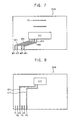
- FIG. 6 is a plan view illustrating a flexible printed circuit board 220A of a display apparatus according to an exemplary embodiment of the present inventive concept.
- FIG. 7 is a plan view illustrating a first layer 222A of FIG. 6 .
- FIG. 8 is a plan view illustrating a second layer 224A of FIG. 6 .
- the display apparatus according to the present exemplary embodiment is substantially the same as the display apparatus of the previous exemplary embodiment described referring to FIGS. 1A to 5 except for the structure of the flexible printed circuit board.
- the same reference numerals will be used to refer to the same or like parts as those described in the previous exemplary embodiment of FIGS. 1A to 5 , and for the convenience of description, the description thereof will be omitted.
- the display apparatus includes a display panel 100 and a panel driver.
- the panel driver includes a printed circuit board (“PCB”) 210 and a plurality of flexible printed circuit board (“FPC”) 220A.
- the display panel 100 displays an image.
- the display panel 100 includes a plurality of gate lines, a plurality of data lines and a plurality of pixels connected to the gate lines and the data lines.
- a first side of the flexible printed circuit board 220A is connected to the display panel 100.
- a second side of the flexible printed circuit board 220A is connected to the printed circuit board 210.
- the flexible printed circuit board 220A is disposed on an upper side of the display panel 100.
- the flexible printed circuit board 220A includes both of a gate driving chip and a source driving chip.
- the gate driving chip and the source driving chip are disposed in a same direction with respect to the display panel 100.
- the flexible printed circuit board 220A includes the first layer 222A and the second layer 224A.
- a first signal transmitting line group ST1, ST2, ST3 and ST4 are disposed on the first layer 222A.
- a second signal transmitting line group GT1 and GT2 and a pad part P1, P2, P3, P4, P5 and P6 are disposed on the second layer 224A.
- the pad part P1 to P6 is connected to the display panel 100.
- the first signal transmitting line group ST1, ST2, ST3 and ST4 is disposed on an upper surface of the first layer 222A.
- the upper surface of the first layer 222A faces toward the printed circuit board 210.
- the second signal transmitting line group GT1 and GT2 and the pad part P1, P2, P3, P4, P5 and P6 are disposed on an upper surface of the second layer 224A.
- the upper surface of the second layer 224A faces toward the first layer 222A.
- a lower surface of the first layer 222A is in contact with the upper surface of the second layer 224A.
- the first signal transmitting line group ST1, ST2, ST3 and ST4 is connected to source pads P1, P2, P4 and P5 of the pad part P1, P2, P3, P4, P5 and P6 disposed on the upper surface of the second layer 224A through pad contact holes HP1, HP2, HP3 and HP4 of the first layer 222A.
- the second signal transmitting line group GT1 and GT2 is directly connected to gate pads P3 and P6 of the pad part P1, P2, P3, P4, P5 and P6 on the second layer 224A.
- the source driving chip SIC is in contact with a first signal transmitting pattern disposed on the upper surface of the first layer 222A.
- the first signal transmitting pattern is a conductive pattern which overlaps the source driving chip SIC.
- the first signal transmitting pattern is directly connected to signal transmitting lines ST1, ST2, ST3 and ST4 of the first signal transmitting line group.
- the gate driving chip GIC is in contact with a second signal transmitting pattern disposed on the upper surface of the second layer 224A through a chip contact hole HC.
- the second signal transmitting pattern is a conductive pattern which overlaps the gate driving chip GIC.
- the second signal transmitting pattern is directly connected to signal transmitting lines GT1 and GT2 of the second signal transmitting line group.
- FIG. 8 is a plan view illustrating only the second layer 224A of the flexible printed circuit board 220A of FIG. 7 .
- the first layer 222A of the flexible printed circuit board 220A is omitted for the convenience of description.
- the gate driving chip GIC is attached to the first layer 222A, not to the second layer 224A.
- the source driving chip SIC and the gate driving chip GIC are disposed adjacent to each other in a vertical direction in the flexible printed circuit board 220A.
- the terms of horizontal and vertical direction reference is made to the description of FIGS. 1A to 5 .
- a width W1 of the first layer 222A in the vertical direction is less than a width W2 of the second layer 224A in the vertical direction so that the pad part P1, P2, P3, P4, P5 and P6 disposed on the upper surface of the second layer 224A is not covered with the first layer 222A. Accordingly, the pad part P1 to P6 is exposed.
- the exposed pad part P1, P2, P3, P4, P5 and P6 is bonded to the display panel 100 so that the exposed pad part P1, P2, P3, P4, P5 and P6 is in contact with an upper surface USF of the display panel 100.
- the source pads P1, P2, P4 and P5 are connected to the data lines DL of the display panel 100.
- Gate pads P3 and P6 of the pad part are connected to the gate lines GLA, GLB1 of the display panel 100.
- the source driving chip SIC and the gate driving chip GIC are disposed on the first layer 222A.
- the present inventive concept is not limited thereto.
- the source driving chip SIC and the gate driving chip GIC may be disposed on the second layer 224A, or the source driving chip SIC and the gate driving chip GIC may be disposed on different layers.
- the source driving chip SIC is disposed in a lower portion and the gate driving chip GIC is disposed in an upper portion in the flexible printed circuit board 220A.
- the second signal transmitting line group GT1 and GT2 detours the area of the source driving chip SIC to be connected to gate pads P3 and P6.
- the source driving chip SIC may be disposed in the upper portion and the gate driving chip GIC may be disposed in the lower portion in the flexible printed circuit board 220A.
- some signal transmitting lines of the first signal transmitting line group may detour the area of the gate driving chip GIC to be connected to source pads P1, P2, P4 and P5.
- the gate driving chip GIC and the source driving chip SIC are disposed adjacent to the upper portion of the display panel 100 so that the width of the bezel at the side portion of the display panel 100 may decrease.
- the gate driving chip GIC and the source driving chip SIC are formed in a single package so that a manufacturing process may be simplified compared to independently manufacturing the gate driving chip GIC and the source driving chip SIC and bonding to each other.
- the gate driving chip GIC and the source driving chip SIC are formed in a single package so that the number of the packages is reduced. Therefore, the manufacturing cost may be reduced.
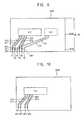
- FIG. 9 is a plan view illustrating a flexible printed circuit board 220B of a display apparatus according to an exemplary embodiment of the present inventive concept.
- FIG. 10 is a plan view illustrating a first layer 222B of FIG. 9 .
- FIG. 11 is a plan view illustrating a second layer 224B of FIG. 9 .
- the display apparatus according to the present exemplary embodiment is substantially the same as the display apparatus of the previous exemplary embodiment described referring to FIGS. 1A to 5 except for the structure of the flexible printed circuit board.
- the same reference numerals will be used to refer to the same or like parts as those described in the previous exemplary embodiment of FIGS. 1A to 5 , and for the convenience of description, the description thereof will be omitted.
- the display apparatus includes a display panel 100 and a panel driver.
- the panel driver includes a printed circuit board (“PCB”) 210 and a plurality of flexible printed circuit board (“FPC”) 220B.
- the display panel 100 displays an image.
- the display panel 100 includes a plurality of gate lines, a plurality of data lines and a plurality of pixels connected to the gate lines and the data lines.
- a first side of the flexible printed circuit board 220B is connected to the display panel 100.
- a second side of the flexible printed circuit board 220B is connected to the printed circuit board 210.
- the flexible printed circuit board 220B is disposed on an upper side of the display panel 100.
- the flexible printed circuit board 220B includes both of a gate driving chip and a source driving chip.
- the gate driving chip and the source driving chip are disposed in a same direction with respect to the display panel 100.
- the flexible printed circuit board 220B includes the first layer 222B and the second layer 224B.
- a first signal transmitting line group ST1, ST2, ST3 and ST4 are disposed on the first layer 222B.
- a second signal transmitting line group GT1 and GT2 and a pad part P1, P2, P3, P4, P5 and P6 are disposed on the second layer 224B.
- the pad part P1 to P6 is connected to the display panel 100.
- the first signal transmitting line group ST1, ST2, ST3 and ST4 is disposed on an upper surface of the first layer 222B.
- the upper surface of the first layer 222B faces toward the printed circuit board 210.
- the second signal transmitting line group GT1 and GT2 and the pad part P1, P2, P3, P4, P5 and P6 are disposed on a lower surface of the second layer 224B.
- the upper surface of the second layer 224B faces toward the first layer 222B.
- a lower surface of the first layer 222B is in contact with the upper surface of the second layer 224B.
- the first signal transmitting line group ST1, ST2, ST3 and ST4 is connected to source pads P1, P2, P4 and P5 of the pad part P1, P2, P3, P4, P5 and P6 disposed on the lower surface of the second layer 224B through first pad contact holes HP1, HP2, HP3 and HP4 of the first layer 222B and second pad contact holes HP5, HP6, HP7 and HP8 of the second layer 224B.
- the second pad contact holes HP5, HP6, HP7 and HP8 are formed from the upper surface of the second layer 224B toward the pad part P1, P2, P3, P4, P5 and P6 disposed on the lower surface of the second layer 224B.
- the second signal transmitting line group GT1 and GT2 is directly connected to gate pads P3 and P6 of the pad part P1, P2, P3, P4, P5 and P6 disposed on the second layer 224B.
- the source driving chip SIC is in contact with a first signal transmitting pattern disposed on the upper surface of the first layer 222B.
- the first signal transmitting pattern is a conductive pattern which overlaps the source driving chip SIC.
- the first signal transmitting pattern is directly connected to signal transmitting lines ST1, ST2, ST3 and ST4 of the first signal transmitting line group.
- the gate driving chip GIC directly is in contact with a second signal transmitting pattern disposed on the lower surface of the second layer 224B.
- the second signal transmitting pattern is a conductive pattern which overlaps the gate driving chip GIC.
- the second signal transmitting pattern is directly connected to signal transmitting lines GT1 and GT2 of the second signal transmitting line group.
- the source driving chip SIC and the gate driving chip GIC are disposed adjacent to each other in a horizontal direction in the flexible printed circuit board 220B. Regarding the terms of horizontal and vertical direction reference is made to the description of FIGS. 1A to 5 .
- a width W1 of the first layer 222B in the vertical direction may be substantially the same as a width W2 of the second layer 224B in the vertical direction.
- the pad part P1, P2, P3, P4, P5 and P6 is disposed on the lower surface of the second layer 224B to be exposed.
- the exposed pad part P1, P2, P3, P4, P5 and P6 is bonded to the display panel 100 so that the exposed pad part P1, P2, P3, P4, P5 and P6 is in contact with an upper surface USF of the display panel 100.
- the source pads P1, P2, P4 and P5 are connected to the data lines DL of the display panel 100.
- the gate pads P3 and P6 are connected to the gate lines GLA, GLB1 of the display panel 100.
- the source driving chip SIC is disposed on the first layer 222B and the gate driving chip GIC is disposed on the second layer 224B.
- the present inventive concept is not limited thereto.
- the source driving chip SIC may be disposed on the second layer 224B and the gate driving chip GIC may be disposed on the first layer 222B.
- the gate driving chip GIC and the source driving chip SIC are disposed adjacent to the upper portion of the display panel 100 so that the width of the bezel at the side portion of the display panel 100 may decrease.
- the gate driving chip GIC and the source driving chip SIC are formed in a single package so that a manufacturing process may be simplified compared to independently manufacturing the gate driving chip GIC and the source driving chip SIC and bonding to each other.
- the gate driving chip GIC and the source driving chip SIC are formed in a single package so that the number of the packages is reduced. Therefore, the manufacturing cost may be reduced.
- one of the gate driving chip GIC and the source driving chip SIC is disposed on an upper surface of the flexible printed circuit board 220B and the other of the gate driving chip GIC and the source driving chip SIC is disposed on a lower surface of the flexible printed circuit board 220B so that pressure is not concentrated to a single surface of the flexible printed circuit board 220B.
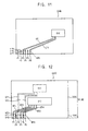
- FIG. 12 is a plan view illustrating a flexible printed circuit board 220C of a display apparatus according to an exemplary embodiment of the present inventive concept.
- FIG. 13 is a plan view illustrating a first layer 222C of FIG. 12 .
- FIG. 14 is a plan view illustrating a second layer 224C of FIG. 12 .
- the display apparatus according to the present exemplary embodiment is substantially the same as the display apparatus of the previous exemplary embodiment described referring to FIGS. 1A to 5 except for the structure of the flexible printed circuit board.
- the same reference numerals will be used to refer to the same or like parts as those described in the previous exemplary embodiment of FIGS. 1A to 5 , and for the convenience of description, the description thereof will be omitted.
- the display apparatus includes a display panel 100 and a panel driver.
- the panel driver includes a printed circuit board (“PCB”) 210 and a plurality of flexible printed circuit board (“FPC”) 220C.
- the display panel 100 displays an image.
- the display panel 100 includes a plurality of gate lines, a plurality of data lines and a plurality of pixels connected to the gate lines and the data lines.
- a first side of the flexible printed circuit board 220C is connected to the display panel 100.
- a second side of the flexible printed circuit board 220C is connected to the printed circuit board 210.
- the flexible printed circuit board 220C is disposed on an upper side of the display panel 100.
- the flexible printed circuit board 220C includes both of a gate driving chip and a source driving chip.
- the gate driving chip and the source driving chip are disposed in a same direction with respect to the display panel 100.
- the flexible printed circuit board 220C includes the first layer 222C and the second layer 224C.
- a first signal transmitting line group ST1, ST2, ST3 and ST4 are disposed on the first layer 222C.
- a second signal transmitting line group GT1 and GT2 and a pad part P1, P2, P3, P4, P5 and P6 connected to the display panel 100 are disposed on the second layer 224C.
- the first signal transmitting line group ST1, ST2, ST3 and ST4 is disposed on an upper surface of the first layer 222C.
- the second signal transmitting line group GT1 and GT2 and the pad part P1, P2, P3, P4, P5 and P6 are disposed on a lower surface of the second layer 224C.
- a lower surface of the first layer 222C is in contact with the upper surface of the second layer 224C.
- the first signal transmitting line group ST1, ST2, ST3 and ST4 is connected to source pads P1, P2, P4 and P5 of the pad part P1, P2, P3, P4, P5 and P6 disposed on the lower surface of the second layer 224C through first pad contact holes HP1, HP2, HP3 and HP4 of the first layer 222C and second pad contact holes HP5, HP6, HP7 and HP8 of the second layer 224C.
- the second pad contact holes HP5, HP6, HP7 and HP8 are formed from the upper surface of the second layer 224C toward the pad part P1, P2, P3, P4, P5 and P6 disposed on the lower surface of the second layer 224C.
- the second signal transmitting line group GT1 and GT2 is connected to gate pads P3 and P6 of the pad part P1, P2, P3, P4, P5 and P6 on the second layer 224C.
- the source driving chip SIC is connected to a first signal transmitting pattern disposed on the upper surface of the first layer 222C.
- the first signal transmitting pattern is a conductive pattern which overlaps the source driving chip SIC.
- the first signal transmitting pattern is directly connected to signal transmitting lines ST1, ST2, ST3 and ST4 of the first signal transmitting line group.
- the gate driving chip GIC is connected to a second signal transmitting pattern disposed on the lower surface of the second layer 224C.
- the second signal transmitting pattern is a conductive pattern which overlaps the gate driving chip GIC.
- the second signal transmitting pattern is directly connected to signal transmitting lines GT1 and GT2 of the second signal transmitting line group.
- the source driving chip SIC and the gate driving chip GIC are disposed adjacent to each other in a vertical direction in the flexible printed circuit board 220C.
- horizontal and vertical direction reference is made to the description of FIGS. 1A to 5 .
- a width W1 of the first layer 222C in the vertical direction may be substantially the same as a width W2 of the second layer 224C in the vertical direction.
- the pad part P1, P2, P3, P4, P5 and P6 is disposed on the lower surface of the second layer 224C to be exposed.
- the exposed pad part P1, P2, P3, P4, P5 and P6 is bonded to the display panel 100 so that the exposed pad part P1, P2, P3, P4, P5 and P6 is connected to an upper surface USF of the display panel 100.
- the source pads P1, P2, P4 and P5 of the pad part are connected to the data lines DL of the display panel 100.
- the gate pads P3 and P6 of the pad part are connected to the gate lines GLA, GLB1 of the display panel 100.
- the source driving chip SIC is disposed on the first layer 222C and the gate driving chip GIC is disposed on the second layer 224C.
- the present inventive concept is not limited thereto.
- the source driving chip SIC may be disposed on the second layer 224C and the gate driving chip GIC may be disposed on the first layer 222C.
- the gate driving chip GIC and the source driving chip SIC are disposed adjacent to the upper portion of the display panel 100 so that the width of the bezel at the side portion of the display panel 100 may decrease.
- the gate driving chip GIC and the source driving chip SIC are formed in a single package so that a manufacturing process may be simplified compared to independently manufacturing the gate driving chip GIC and the source driving chip SIC and bonding to each other.
- the gate driving chip GIC and the source driving chip SIC are formed in a single package so that the number of the packages is reduced. Therefore, the manufacturing cost may be reduced.
- one of the gate driving chip GIC and the source driving chip SIC is disposed on an upper surface of the flexible printed circuit board 220C and the other of the gate driving chip GIC and the source driving chip SIC is disposed on a lower surface of the flexible printed circuit board 220C so that pressure is not concentrated to a single surface of the flexible printed circuit board 220C.
- FIG. 15 is a plan view illustrating a flexible printed circuit board 220D of a display apparatus according to an exemplary embodiment of the present inventive concept.
- the display apparatus according to the present exemplary embodiment is substantially the same as the display apparatus of the previous exemplary embodiment described referring to FIGS. 1A to 5 except for the structure of the flexible printed circuit board.
- the same reference numerals will be used to refer to the same or like parts as those described in the previous exemplary embodiment of FIGS. 1A to 5 , and for the convenience of description, the description thereof will be omitted.
- the display apparatus includes a display panel 100 and a panel driver.
- the panel driver includes a printed circuit board (“PCB”) 210 and a plurality of flexible printed circuit board (“FPC”) 220D.
- the display panel 100 displays an image.
- the display panel 100 includes a plurality of gate lines, a plurality of data lines and a plurality of pixels connected to the gate lines and the data lines.
- a first side of the flexible printed circuit board 220D is connected to the display panel 100.
- a second side of the flexible printed circuit board 220D is connected to the printed circuit board 210.
- the flexible printed circuit board 220D is disposed on the display panel 100.
- the flexible printed circuit board 220D may be disposed on an upper side of the display panel 100.
- the flexible printed circuit board 220D includes a gate driving chip and a source driving chip.
- the gate driving chip and the source driving chip are disposed in a same direction with respect to the display panel 100.
- the flexible printed circuit board 220D has a single layer structure.
- the flexible printed circuit board 220D includes a base substrate on which a first signal transmitting line group ST1, ST2, ..., STN-1 and STN, a second signal transmitting line group GT1, GT2, ..., GTM-1 and GTM and a pad part PS1, PS2, ..., PSN-1, PSN, PG1, PG2, ..., PGM-1 and PGM connected to the display panel 100 are disposed.
- the first signal transmitting line group ST1, ST2, ..., STN-1 and STN, the second signal transmitting line group GT1, GT2, ..., GTM-1 and GTM and the pad part PS1, PS2, ..., PSN-1, PSN, PG1, PG2, ..., PGM-1, PGM are disposed on an upper surface of the base substrate.
- the first signal transmitting line group ST1, ST2, ..., STN-1 and STN is connected to source pads PS1, PS2, ..., PSN-1 and PSN of the pad part disposed on the base substrate.
- the second signal transmitting line group GT1, GT2, ..., GTM-1 and GTM is connected to gate pads PG1, PG2, ..., PGM-1 and PGM of the pad part disposed on the base substrate.
- the source driving chip SIC is in contact with a first signal transmitting pattern disposed on the upper surface of the base substrate.
- the first signal transmitting pattern is a conductive pattern which overlaps the source driving chip SIC.
- the first signal transmitting pattern is connected to signal transmitting lines ST1, ST2, ..., STN-1 and STN of the first signal transmitting line group.
- the gate driving chip GIC is in contact with a second signal transmitting pattern disposed on the upper surface of the base substrate.
- the second signal transmitting pattern is a conductive pattern which overlaps the gate driving chip GIC.
- the second signal transmitting pattern is connected to signal transmitting lines GT1, GT2, ..., GTM-1 and GTM of the second signal transmitting line group.
- the source driving chip SIC and the gate driving chip GIC are disposed adjacent to each other in a horizontal direction in the flexible printed circuit board 220D.
- horizontal and vertical direction reference is made to the description of FIGS 1 1 to 5 .
- the exposed pad part PS1, PS2, ..., PSN-1, PSN, PG1, PG2, ..., PGM-1 and PGM is bonded to the display panel 100 so that the exposed pad part PS1, PS2, ..., PSN-1, PSN, PG1, PG2, ..., PGM-1 and PGM is in contact with an upper surface USF of the display panel 100.
- Source pads PS1, PS2, ..., PSN-1 and PSN of the pad part are connected to the data lines DL of the display panel 100.
- Gate pads PG1, PG2, ..., PGM-1 and PGM of the pad part are connected to the gate lines GLA, GLB1 of the display panel 100.
- the signal transmitting lines ST1, ST2, ..., STN-1 and STN of the first signal transmitting line group do not cross the signal transmitting lines GT1, GT2, ..., GTM-1 and GTM of the second signal transmitting line group.
- the gate driving chip GIC and the source driving chip SIC are disposed adjacent to the upper portion of the display panel 100 so that the width of the bezel at the side portion of the display panel 100 may decrease.
- the gate driving chip GIC and the source driving chip SIC are formed in a single package so that a manufacturing process may be simplified compared to independently manufacturing the gate driving chip GIC and the source driving chip SIC and bonding to each other.
- the gate driving chip GIC and the source driving chip SIC are formed in a single package so that the number of the packages is reduced. Therefore, the manufacturing cost may be reduced.
- a width of the bezel of the display apparatus may decrease, a process of manufacturing the display apparatus may be simplified and a manufacturing cost of the display apparatus may be reduced.
Landscapes
- Engineering & Computer Science (AREA)
- Physics & Mathematics (AREA)
- General Physics & Mathematics (AREA)
- Computer Hardware Design (AREA)
- Theoretical Computer Science (AREA)
- Microelectronics & Electronic Packaging (AREA)
- Nonlinear Science (AREA)
- Mathematical Physics (AREA)
- Chemical & Material Sciences (AREA)
- Crystallography & Structural Chemistry (AREA)
- Optics & Photonics (AREA)
- Manufacturing & Machinery (AREA)
- Devices For Indicating Variable Information By Combining Individual Elements (AREA)
- Liquid Crystal (AREA)
Abstract
Description
- The present inventive concept relates to a display apparatus.
- Generally, a display apparatus includes a display panel and a display panel driver. The display driver may be disposed within a bezel portion of the display panel.
- According to an exemplary embodiment, a display apparatus is provided. The display apparatus includes a display panel and a plurality of flexible printed circuit boards. The display panel includes a gate line and a data line. The plurality of flexible printed circuit boards is connected to one side of the display panel. Each of the plurality of flexible printed circuit board includes a gate driving chip configured to apply a gate signal to the gate line and a source driving chip configured to apply a data voltage to the data line.
- According to an exemplary embodiment of the present inventive concept, a display apparatus is provided. The display apparatus includes a display panel, a plurality of flexible circuit boards and a printed circuit board. The display panel includes a gate line and a data line. The plurality of flexible printed circuit boards is connected to one side of the display panel. Each of the plurality of flexible printed circuit board includes a gate driving chip configured to apply a gate signal to the gate line and a source driving chip configured to apply a data voltage to the data line. A printed circuit board is configured to apply a gate control signal to the gate driving chip and a data control signal to the source driving chip. The printed circuit board is connected to the plurality of flexible printed circuit boards. The plurality of flexible printed circuit boards is disposed between the printed circuit board and the display panel. The display panel, the plurality of flexible printed circuit boards and the printed circuit board are arranged in a first direction, and each of the plurality of flexible printed circuit boards is arranged in a second direction crossing the first direction.
- These and other features of the inventive concept will become more apparent by describing in detail exemplary embodiments thereof with reference to the accompanying drawings of which:
-
FIG. 1A is a plan view illustrating a display apparatus according to an exemplary embodiment of the present inventive concept; -
FIG. 1B is a sectional view illustrating the display apparatus ofFIG. 1A ; -
FIG. 2 is a plan view illustrating a display panel ofFIG. 1A ; -
FIG. 3 is a plan view illustrating a flexible printed circuit board ofFIG. 1A ; -
FIG. 4 is a plan view illustrating a first layer ofFIG. 3 ; -
FIG. 5 is a plan view illustrating a second layer ofFIG. 3 ; -
FIG. 6 is a plan view illustrating a flexible printed circuit board of a display apparatus according to an exemplary embodiment of the present inventive concept; -
FIG. 7 is a plan view illustrating a first layer ofFIG. 6 ; -
FIG. 8 is a plan view illustrating a second layer ofFIG. 6 ; -
FIG. 9 is a plan view illustrating a flexible printed circuit board of a display apparatus according to an exemplary embodiment of the present inventive concept; -
FIG. 10 is a plan view illustrating a first layer ofFIG. 9 ; -
FIG. 11 is a plan view illustrating a second layer ofFIG. 9 ; -
FIG. 12 is a plan view illustrating a flexible printed circuit board of a display apparatus according to an exemplary embodiment of the present inventive concept; -
FIG. 13 is a plan view illustrating a first layer ofFIG. 12 ; -
FIG. 14 is a plan view illustrating a second layer ofFIG. 12 ; and -
FIG. 15 is a plan view illustrating a flexible printed circuit board of a display apparatus according to an exemplary embodiment of the present inventive concept. - Exemplary embodiments of the inventive concept will be described below in detail with reference to the accompanying drawings. However, the inventive concept may be embodied in different forms and should not be construed as limited to the embodiments set forth herein. In the drawings, the thickness of layers and regions may be exaggerated for clarity. It will also be understood that when an element is referred to as being "on" another element or substrate, it may be directly on the other element or substrate, or intervening layers may also be present. It will also be understood that when an element is referred to as being "coupled to" or "connected to" another element, it may be directly coupled to or connected to the other element, or intervening elements may also be present. Like reference numerals may refer to the like elements throughout the specification and drawings. Hereinafter, the present inventive concept will be described in detail with reference to the accompanying drawings.
-
FIG. 1A is a plan view illustrating a display apparatus according to an exemplary embodiment of the present inventive concept.FIG. 1B is a sectional view illustrating the display apparatus ofFIG. 1A . - Referring to
FIGS. 1A and 1B , the display apparatus includes adisplay panel 100 and a panel driver. The panel driver includes a printed circuit board ("PCB") 210 and a plurality of flexible printed circuit board ("FPC") 220. - The
display panel 100 displays an image. Thedisplay panel 100 includes a plurality of gate lines, a plurality of data lines and a plurality of pixels connected to the gate lines and the data lines. - Each pixel includes a switching element (not shown), a liquid crystal capacitor (not shown) and a storage capacitor (not shown). The liquid crystal capacitor and the storage capacitor are electrically connected to the switching element. The pixels may be disposed in a matrix form.
- A structure of the
display panel 100 is described referring toFIG. 2 in detail. - A first side of the flexible printed
circuit board 220 is connected to thedisplay panel 100. The first side of the flexible printedcircuit board 220 is connected to an upper surface USF of thedisplay panel 100. A second side of the flexible printedcircuit board 220 is connected to the printedcircuit board 210. - The flexible printed
circuit board 220 includes a flexible material. The flexible printedcircuit board 220 may cover the side surface SSF of thedisplay panel 100, and the printedcircuit board 210 may be bended toward a lower surface LSF of thedisplay panel 100, covering the side surface SSF of thedisplay panel 100. - For example, the flexible printed
circuit board 220 is disposed on an upper side of thedisplay panel 100. - The flexible printed
circuit board 220 includes both of a gate driving chip and a source driving chip. Thus, the gate driving chip and the source driving chip are preferably disposed in a same direction with respect to thedisplay panel 100, which means that the gate driving chip and the source driving chip may be aligned with each other. - A structure of the flexible printed
circuit board 220 will be described referring toFIGS. 3 to 5 in detail. - The printed
circuit board 210 may include a timing controller. The timing controller receives input image data and an input control signal from an external apparatus. The input image data may include red image data, green image data and blue image data. The input control signal may include a master clock signal and a data enable signal. The input control signal may further include a vertical synchronizing signal and a horizontal synchronizing signal. - The timing controller generates a gate control signal, a data control signal and data based on the input image data and the input control signal.
- The timing controller generates the gate control signal for controlling an operation of the gate driving chip based on the input control signal, and outputs the gate control signal to the gate driving chip. The gate control signal may include a vertical start signal and a gate clock signal.
- The timing controller generates the data control signal for controlling an operation of the source driving chip based on the input control signal, and outputs the data control signal to the source driving chip. The data control signal may include a horizontal start signal and a load signal.
- The timing controller generates the data signal based on the input image data. The timing controller outputs the data signal to the source driving chip.
- The gate driving chip generates gate signals to drive the gate lines in response to a first control signal received from the timing controller. The gate driving chip sequentially outputs the gate signals to the gate lines.
- The gate driving chip may be connected to the
display panel 100 as a tape carrier package (TCP) type. - The source driving chip receives the data control signal and the data signal from the timing controller, and receives gamma reference voltages from a gamma reference voltage generator. The source driving chip converts the data signal into data voltages having an analog type using the gamma reference voltages. The source driving chip outputs the data voltages to the data lines.
- The source driving chip may be connected to the
display panel 100 in a TCP type. -
FIG. 2 is a plan view illustrating thedisplay panel 100 ofFIG. 1A . - Referring to
FIGS. 1A, 1B and2 , the gate driving chip and the source driving chip may be disposed adjacent to an upper portion of thedisplay panel 100. - The
display panel 100 is divided into a first area A and a second area B. The first area A is defined as a left and upper portion of an inclined dotted line extending from a right vertex of an upper side of thedisplay panel 100 to a lower side of thedisplay panel 100. The second area B is defined as a right and lower portion of the inclined dotted line. - The first area A is driven by a first gate line group GLA extending in an inclined direction. The second area B is driven by a second gate line group GLB1 extending in a vertical direction and a third gate line group GLB2 connected to the second gate line group and extending in the inclined direction from an end portion of the second gate line group. The second gate line group GLB1 is connected, at the lower side of the
display panel 100, to the third gate line group GLB2. - For example, a gate line in the first gate line group and a gate line in the third gate line group may extend stepwise.
- The data lines DL of the
display panel 100 may extend in a vertical direction in both areas, the first and second areas A and B of the display panel. -
FIG. 3 is a plan view illustrating the flexible printedcircuit board 220 ofFIG. 1A .FIG. 4 is a plan view illustrating afirst layer 222 ofFIG. 3 .FIG. 5 is a plan view illustrating asecond layer 224 ofFIG. 3 . - Referring to
FIGS. 1A to 5 , the flexible printedcircuit board 220 includes thefirst layer 222 and thesecond layer 224. A first signal transmitting line group ST1, ST2, ST3 and ST4 are disposed on thefirst layer 222. A second signal transmitting line group GT1 and GT2 and a pad part P1, P2, P3, P4, P5 and P6 are disposed on thesecond layer 224. The pad part P1 to P6 is connected to thedisplay panel 100. - The first signal transmitting line group ST1, ST2, ST3 and ST4 is disposed on an upper surface of the
first layer 222. The upper surface of thefirst layer 222 faces toward the printedcircuit board 210. The second signal transmitting line group GT1 and GT2 and the pad part P1, P2, P3, P4, P5 and P6 are disposed on an upper surface of thesecond layer 224. The upper surface of thesecond layer 224 faces toward thefirst layer 222. A lower surface of thefirst layer 222 is in contact with the upper surface of thesecond layer 224. - The first signal transmitting line group ST1, ST2, ST3 and ST4 is connected to source pads P1, P2, P4 and P5 of the pad part P1, P2, P3, P4, P5 and P6 disposed on the upper surface of the
second layer 224 through pad contact holes HP1, HP2, HP3 and HP4 of thefirst layer 222. - The second signal transmitting line group GT1 and GT2 is directly connected to gate pads P3 and P6 of the pad part P1, P2, P3, P4, P5 and P6 on the
second layer 224. - In the present exemplary embodiment, the source driving chip SIC is connected to a first signal transmitting pattern disposed on the upper surface of the
first layer 222. The first signal transmitting pattern is a conductive pattern which overlaps the source driving chip SIC. The first signal transmitting pattern is directly connected to signal transmitting lines ST1, ST2, ST3 and ST4 of the first signal transmitting line group. - The gate driving chip GIC is in contact with a second signal transmitting pattern disposed on the upper surface of the
second layer 224 through a chip contact hole HC. The second signal transmitting pattern is a conductive pattern which overlaps the gate driving chip GIC. The second signal transmitting pattern is directly connected to signal transmitting lines GT1 and GT2 of the second signal transmitting line group. -
FIG. 5 is a plan view illustrating only thesecond layer 224 of the flexible printedcircuit board 220 ofFIG. 3 . InFIG. 5 , thefirst layer 222 of the flexible printedcircuit board 220 is omitted for the convenience of description. InFIG. 5 , the gate driving chip GIC is in contact with thefirst layer 222, not to thesecond layer 222. - Two first signal transmitting lines and one second signal transmitting line are alternately connected to the pads of the pad part. For example, the second signal transmitting line GT1 is connected to the pad P3 which is interposed between first two pads P1 and P2, and second two pads P4 and P5. The first two pads P1 and P2 are connected to two first signal transmitting lines ST1 and ST2. The second two pads P4 and P5 are connected to two first signal transmitting lines ST3 and ST4. In such connections, the two first signal transmitting lines ST3 and ST4 cross the second signal transmitting line GT1, when viewed from the above.
- The gate driving chip GIC and the source driving chip SIC are disposed on the upper surface of the
first layer 222. A bump part of the source driving chip SIC are disposed on thefirst layer 222 to be in contact with the first signal transmitting pattern on the upper surface of thefirst layer 222. - A bump part of the gate driving chip GIC is disposed on the
first layer 222. The bump part of the gate driving chip GIC is in contact with the second signal transmitting pattern protruded from the upper surface of thesecond surface 224 toward the chip contact hole HC. Alternatively, the bump part of the gate driving chip GIC may pass through the chip contact hole HC to be in contact with the second signal transmitting pattern. Although the bump part of the gate driving chip GIC passes through the chip contact hole HC, the main body of the gate driving chip GIC is disposed on the upper surface of thefirst layer 222 so that the gate driving chip GIC is regarded as to be disposed on the upper surface of thefirst layer 222. - In the present exemplary embodiment, the source driving chip SIC and the gate driving chip GIC are disposed adjacent to each other in a horizontal direction in the flexible printed
circuit board 220, here in a direction corresponding to the extension of the sides of the display panel which have a greater width than sides in a vertical direction of the display panel with a relative smaller width and extending perpendicular on the sides in the horizontal direction. However, this is just a preferable embodiment and not necessary in any case. - In the present exemplary embodiment, a width W1 of the
first layer 222 in the vertical direction is less than a width W2 of thesecond layer 224 in the vertical direction so that the pad part P1, P2, P3, P4, P5 and P6 disposed on the upper surface of thesecond layer 224 is not covered with the first layer 22. Accordingly, the pad part P1 to P6 is exposed. - The exposed pad part P1, P2, P3, P4, P5 and P6 is bonded to the
display panel 100 so that the exposed pad part P1, P2, P3, P4, P5 and P6 is in contact with an upper surface USF of thedisplay panel 100. The source pads P1, P2, P4 and P5 are connected to the data lines DL of thedisplay panel 100. Gate pads P3 and P6 of the pad part are connected to the gate lines GLA, GLB1 of thedisplay panel 100. - According to an exemplary embodiment, the source driving chip SIC and the gate driving chip GIC are disposed on the
first layer 222. However, the present inventive concept is not limited thereto. For example, the source driving chip SIC and the gate driving chip GIC may be disposed on thesecond layer 224, or the source driving chip SIC and the gate driving chip GIC may be disposed on different layers. - Although the source driving chip SIC is disposed at a left side and the gate driving chip GIC is disposed at a right side in the flexible printed
circuit board 220 in the present exemplary embodiment, the present exemplary embodiment is not limited thereto. For example, the source driving chip SIC may be disposed at a right side and the gate driving chip GIC may be disposed at a left side in the flexible printedcircuit board 220. - According to the present exemplary embodiment, the gate driving chip GIC and the source driving chip SIC are disposed adjacent to the upper portion of the
display panel 100 so that the width of the bezel at the side portion of thedisplay panel 100 may decrease. - In addition, the gate driving chip GIC and the source driving chip SIC are formed in a single package so that a manufacturing process may be simplified compared to independently manufacturing the gate driving chip GIC and the source driving chip SIC and bonding to each other.
- In addition, the gate driving chip GIC and the source driving chip SIC are formed in a single package so that the number of the packages is reduced. Therefore, the manufacturing cost may be reduced.
-
FIG. 6 is a plan view illustrating a flexible printedcircuit board 220A of a display apparatus according to an exemplary embodiment of the present inventive concept.FIG. 7 is a plan view illustrating afirst layer 222A ofFIG. 6 .FIG. 8 is a plan view illustrating asecond layer 224A ofFIG. 6 . - The display apparatus according to the present exemplary embodiment is substantially the same as the display apparatus of the previous exemplary embodiment described referring to
FIGS. 1A to 5 except for the structure of the flexible printed circuit board. Thus, the same reference numerals will be used to refer to the same or like parts as those described in the previous exemplary embodiment ofFIGS. 1A to 5 , and for the convenience of description, the description thereof will be omitted. - Referring to
FIGS. 1A, 1B ,2 ,6 to 8 , the display apparatus includes adisplay panel 100 and a panel driver. The panel driver includes a printed circuit board ("PCB") 210 and a plurality of flexible printed circuit board ("FPC") 220A. - The
display panel 100 displays an image. Thedisplay panel 100 includes a plurality of gate lines, a plurality of data lines and a plurality of pixels connected to the gate lines and the data lines. - A first side of the flexible printed
circuit board 220A is connected to thedisplay panel 100. A second side of the flexible printedcircuit board 220A is connected to the printedcircuit board 210. - For example, the flexible printed
circuit board 220A is disposed on an upper side of thedisplay panel 100. - The flexible printed
circuit board 220A includes both of a gate driving chip and a source driving chip. Thus, the gate driving chip and the source driving chip are disposed in a same direction with respect to thedisplay panel 100. - The flexible printed
circuit board 220A includes thefirst layer 222A and thesecond layer 224A. A first signal transmitting line group ST1, ST2, ST3 and ST4 are disposed on thefirst layer 222A. A second signal transmitting line group GT1 and GT2 and a pad part P1, P2, P3, P4, P5 and P6 are disposed on thesecond layer 224A. The pad part P1 to P6 is connected to thedisplay panel 100. - The first signal transmitting line group ST1, ST2, ST3 and ST4 is disposed on an upper surface of the
first layer 222A. The upper surface of thefirst layer 222A faces toward the printedcircuit board 210. The second signal transmitting line group GT1 and GT2 and the pad part P1, P2, P3, P4, P5 and P6 are disposed on an upper surface of thesecond layer 224A. The upper surface of thesecond layer 224A faces toward thefirst layer 222A. A lower surface of thefirst layer 222A is in contact with the upper surface of thesecond layer 224A. - The first signal transmitting line group ST1, ST2, ST3 and ST4 is connected to source pads P1, P2, P4 and P5 of the pad part P1, P2, P3, P4, P5 and P6 disposed on the upper surface of the
second layer 224A through pad contact holes HP1, HP2, HP3 and HP4 of thefirst layer 222A. - The second signal transmitting line group GT1 and GT2 is directly connected to gate pads P3 and P6 of the pad part P1, P2, P3, P4, P5 and P6 on the
second layer 224A. - In the present exemplary embodiment, the source driving chip SIC is in contact with a first signal transmitting pattern disposed on the upper surface of the
first layer 222A. The first signal transmitting pattern is a conductive pattern which overlaps the source driving chip SIC. The first signal transmitting pattern is directly connected to signal transmitting lines ST1, ST2, ST3 and ST4 of the first signal transmitting line group. - The gate driving chip GIC is in contact with a second signal transmitting pattern disposed on the upper surface of the
second layer 224A through a chip contact hole HC. The second signal transmitting pattern is a conductive pattern which overlaps the gate driving chip GIC. The second signal transmitting pattern is directly connected to signal transmitting lines GT1 and GT2 of the second signal transmitting line group. -
FIG. 8 is a plan view illustrating only thesecond layer 224A of the flexible printedcircuit board 220A ofFIG. 7 . InFIG. 8 , thefirst layer 222A of the flexible printedcircuit board 220A is omitted for the convenience of description. InFIG. 8 , the gate driving chip GIC is attached to thefirst layer 222A, not to thesecond layer 224A. - In the present exemplary embodiment, the source driving chip SIC and the gate driving chip GIC are disposed adjacent to each other in a vertical direction in the flexible printed
circuit board 220A. Regarding the terms of horizontal and vertical direction reference is made to the description ofFIGS. 1A to 5 . - In the present exemplary embodiment, a width W1 of the
first layer 222A in the vertical direction is less than a width W2 of thesecond layer 224A in the vertical direction so that the pad part P1, P2, P3, P4, P5 and P6 disposed on the upper surface of thesecond layer 224A is not covered with thefirst layer 222A. Accordingly, the pad part P1 to P6 is exposed. - The exposed pad part P1, P2, P3, P4, P5 and P6 is bonded to the
display panel 100 so that the exposed pad part P1, P2, P3, P4, P5 and P6 is in contact with an upper surface USF of thedisplay panel 100. The source pads P1, P2, P4 and P5 are connected to the data lines DL of thedisplay panel 100. Gate pads P3 and P6 of the pad part are connected to the gate lines GLA, GLB1 of thedisplay panel 100. - According to an exemplary embodiment, the source driving chip SIC and the gate driving chip GIC are disposed on the
first layer 222A. However, the present inventive concept is not limited thereto. For example, the source driving chip SIC and the gate driving chip GIC may be disposed on thesecond layer 224A, or the source driving chip SIC and the gate driving chip GIC may be disposed on different layers. - The source driving chip SIC is disposed in a lower portion and the gate driving chip GIC is disposed in an upper portion in the flexible printed
circuit board 220A. The second signal transmitting line group GT1 and GT2 detours the area of the source driving chip SIC to be connected to gate pads P3 and P6. - The present inventive concept is not limited thereto. For example, the source driving chip SIC may be disposed in the upper portion and the gate driving chip GIC may be disposed in the lower portion in the flexible printed
circuit board 220A. In this case, some signal transmitting lines of the first signal transmitting line group may detour the area of the gate driving chip GIC to be connected to source pads P1, P2, P4 and P5. - According to the present exemplary embodiment, the gate driving chip GIC and the source driving chip SIC are disposed adjacent to the upper portion of the
display panel 100 so that the width of the bezel at the side portion of thedisplay panel 100 may decrease. - In addition, the gate driving chip GIC and the source driving chip SIC are formed in a single package so that a manufacturing process may be simplified compared to independently manufacturing the gate driving chip GIC and the source driving chip SIC and bonding to each other.
- In addition, the gate driving chip GIC and the source driving chip SIC are formed in a single package so that the number of the packages is reduced. Therefore, the manufacturing cost may be reduced.
-
FIG. 9 is a plan view illustrating a flexible printedcircuit board 220B of a display apparatus according to an exemplary embodiment of the present inventive concept.FIG. 10 is a plan view illustrating afirst layer 222B ofFIG. 9 .FIG. 11 is a plan view illustrating asecond layer 224B ofFIG. 9 . - The display apparatus according to the present exemplary embodiment is substantially the same as the display apparatus of the previous exemplary embodiment described referring to
FIGS. 1A to 5 except for the structure of the flexible printed circuit board. Thus, the same reference numerals will be used to refer to the same or like parts as those described in the previous exemplary embodiment ofFIGS. 1A to 5 , and for the convenience of description, the description thereof will be omitted. - Referring to
FIGS. 1A, 1B ,2 ,9 to 11 , the display apparatus includes adisplay panel 100 and a panel driver. The panel driver includes a printed circuit board ("PCB") 210 and a plurality of flexible printed circuit board ("FPC") 220B. - The
display panel 100 displays an image. Thedisplay panel 100 includes a plurality of gate lines, a plurality of data lines and a plurality of pixels connected to the gate lines and the data lines. - A first side of the flexible printed
circuit board 220B is connected to thedisplay panel 100. A second side of the flexible printedcircuit board 220B is connected to the printedcircuit board 210. - For example, the flexible printed
circuit board 220B is disposed on an upper side of thedisplay panel 100. - The flexible printed
circuit board 220B includes both of a gate driving chip and a source driving chip. Thus, the gate driving chip and the source driving chip are disposed in a same direction with respect to thedisplay panel 100. - The flexible printed
circuit board 220B includes thefirst layer 222B and thesecond layer 224B. A first signal transmitting line group ST1, ST2, ST3 and ST4 are disposed on thefirst layer 222B. A second signal transmitting line group GT1 and GT2 and a pad part P1, P2, P3, P4, P5 and P6 are disposed on thesecond layer 224B. The pad part P1 to P6 is connected to thedisplay panel 100. - The first signal transmitting line group ST1, ST2, ST3 and ST4 is disposed on an upper surface of the
first layer 222B. The upper surface of thefirst layer 222B faces toward the printedcircuit board 210. The second signal transmitting line group GT1 and GT2 and the pad part P1, P2, P3, P4, P5 and P6 are disposed on a lower surface of thesecond layer 224B. The upper surface of thesecond layer 224B faces toward thefirst layer 222B. A lower surface of thefirst layer 222B is in contact with the upper surface of thesecond layer 224B. - The first signal transmitting line group ST1, ST2, ST3 and ST4 is connected to source pads P1, P2, P4 and P5 of the pad part P1, P2, P3, P4, P5 and P6 disposed on the lower surface of the
second layer 224B through first pad contact holes HP1, HP2, HP3 and HP4 of thefirst layer 222B and second pad contact holes HP5, HP6, HP7 and HP8 of thesecond layer 224B. The second pad contact holes HP5, HP6, HP7 and HP8 are formed from the upper surface of thesecond layer 224B toward the pad part P1, P2, P3, P4, P5 and P6 disposed on the lower surface of thesecond layer 224B. - The second signal transmitting line group GT1 and GT2 is directly connected to gate pads P3 and P6 of the pad part P1, P2, P3, P4, P5 and P6 disposed on the
second layer 224B. - In the present exemplary embodiment, the source driving chip SIC is in contact with a first signal transmitting pattern disposed on the upper surface of the
first layer 222B. The first signal transmitting pattern is a conductive pattern which overlaps the source driving chip SIC. The first signal transmitting pattern is directly connected to signal transmitting lines ST1, ST2, ST3 and ST4 of the first signal transmitting line group. - The gate driving chip GIC directly is in contact with a second signal transmitting pattern disposed on the lower surface of the
second layer 224B. The second signal transmitting pattern is a conductive pattern which overlaps the gate driving chip GIC. The second signal transmitting pattern is directly connected to signal transmitting lines GT1 and GT2 of the second signal transmitting line group. - In the present exemplary embodiment, the source driving chip SIC and the gate driving chip GIC are disposed adjacent to each other in a horizontal direction in the flexible printed
circuit board 220B. Regarding the terms of horizontal and vertical direction reference is made to the description ofFIGS. 1A to 5 . - In the present exemplary embodiment, a width W1 of the
first layer 222B in the vertical direction may be substantially the same as a width W2 of thesecond layer 224B in the vertical direction. The pad part P1, P2, P3, P4, P5 and P6 is disposed on the lower surface of thesecond layer 224B to be exposed. - The exposed pad part P1, P2, P3, P4, P5 and P6 is bonded to the
display panel 100 so that the exposed pad part P1, P2, P3, P4, P5 and P6 is in contact with an upper surface USF of thedisplay panel 100. The source pads P1, P2, P4 and P5 are connected to the data lines DL of thedisplay panel 100. The gate pads P3 and P6 are connected to the gate lines GLA, GLB1 of thedisplay panel 100. - According to an exemplary embodiment, the source driving chip SIC is disposed on the
first layer 222B and the gate driving chip GIC is disposed on thesecond layer 224B. The present inventive concept is not limited thereto. Alternatively, the source driving chip SIC may be disposed on thesecond layer 224B and the gate driving chip GIC may be disposed on thefirst layer 222B. - According to the present exemplary embodiment, the gate driving chip GIC and the source driving chip SIC are disposed adjacent to the upper portion of the
display panel 100 so that the width of the bezel at the side portion of thedisplay panel 100 may decrease. - In addition, the gate driving chip GIC and the source driving chip SIC are formed in a single package so that a manufacturing process may be simplified compared to independently manufacturing the gate driving chip GIC and the source driving chip SIC and bonding to each other.
- In addition, the gate driving chip GIC and the source driving chip SIC are formed in a single package so that the number of the packages is reduced. Therefore, the manufacturing cost may be reduced.
- In addition, one of the gate driving chip GIC and the source driving chip SIC is disposed on an upper surface of the flexible printed
circuit board 220B and the other of the gate driving chip GIC and the source driving chip SIC is disposed on a lower surface of the flexible printedcircuit board 220B so that pressure is not concentrated to a single surface of the flexible printedcircuit board 220B. -
FIG. 12 is a plan view illustrating a flexible printedcircuit board 220C of a display apparatus according to an exemplary embodiment of the present inventive concept.FIG. 13 is a plan view illustrating afirst layer 222C ofFIG. 12 .FIG. 14 is a plan view illustrating asecond layer 224C ofFIG. 12 . - The display apparatus according to the present exemplary embodiment is substantially the same as the display apparatus of the previous exemplary embodiment described referring to
FIGS. 1A to 5 except for the structure of the flexible printed circuit board. Thus, the same reference numerals will be used to refer to the same or like parts as those described in the previous exemplary embodiment ofFIGS. 1A to 5 , and for the convenience of description, the description thereof will be omitted. - Referring to
FIGS. 1A, 1B ,2 ,12 to 14 , the display apparatus includes adisplay panel 100 and a panel driver. The panel driver includes a printed circuit board ("PCB") 210 and a plurality of flexible printed circuit board ("FPC") 220C. - The
display panel 100 displays an image. Thedisplay panel 100 includes a plurality of gate lines, a plurality of data lines and a plurality of pixels connected to the gate lines and the data lines. - A first side of the flexible printed
circuit board 220C is connected to thedisplay panel 100. A second side of the flexible printedcircuit board 220C is connected to the printedcircuit board 210. - For example, the flexible printed
circuit board 220C is disposed on an upper side of thedisplay panel 100. - The flexible printed
circuit board 220C includes both of a gate driving chip and a source driving chip. Thus, the gate driving chip and the source driving chip are disposed in a same direction with respect to thedisplay panel 100. - The flexible printed
circuit board 220C includes thefirst layer 222C and thesecond layer 224C. A first signal transmitting line group ST1, ST2, ST3 and ST4 are disposed on thefirst layer 222C. A second signal transmitting line group GT1 and GT2 and a pad part P1, P2, P3, P4, P5 and P6 connected to thedisplay panel 100 are disposed on thesecond layer 224C. - The first signal transmitting line group ST1, ST2, ST3 and ST4 is disposed on an upper surface of the
first layer 222C. The second signal transmitting line group GT1 and GT2 and the pad part P1, P2, P3, P4, P5 and P6 are disposed on a lower surface of thesecond layer 224C. A lower surface of thefirst layer 222C is in contact with the upper surface of thesecond layer 224C. - The first signal transmitting line group ST1, ST2, ST3 and ST4 is connected to source pads P1, P2, P4 and P5 of the pad part P1, P2, P3, P4, P5 and P6 disposed on the lower surface of the
second layer 224C through first pad contact holes HP1, HP2, HP3 and HP4 of thefirst layer 222C and second pad contact holes HP5, HP6, HP7 and HP8 of thesecond layer 224C. The second pad contact holes HP5, HP6, HP7 and HP8 are formed from the upper surface of thesecond layer 224C toward the pad part P1, P2, P3, P4, P5 and P6 disposed on the lower surface of thesecond layer 224C. - The second signal transmitting line group GT1 and GT2 is connected to gate pads P3 and P6 of the pad part P1, P2, P3, P4, P5 and P6 on the
second layer 224C. - In the present exemplary embodiment, the source driving chip SIC is connected to a first signal transmitting pattern disposed on the upper surface of the
first layer 222C. The first signal transmitting pattern is a conductive pattern which overlaps the source driving chip SIC. The first signal transmitting pattern is directly connected to signal transmitting lines ST1, ST2, ST3 and ST4 of the first signal transmitting line group. - The gate driving chip GIC is connected to a second signal transmitting pattern disposed on the lower surface of the
second layer 224C. The second signal transmitting pattern is a conductive pattern which overlaps the gate driving chip GIC. The second signal transmitting pattern is directly connected to signal transmitting lines GT1 and GT2 of the second signal transmitting line group. - In the present exemplary embodiment, the source driving chip SIC and the gate driving chip GIC are disposed adjacent to each other in a vertical direction in the flexible printed
circuit board 220C. Regarding the terms of horizontal and vertical direction reference is made to the description ofFIGS. 1A to 5 . - In the present exemplary embodiment, a width W1 of the
first layer 222C in the vertical direction may be substantially the same as a width W2 of thesecond layer 224C in the vertical direction. The pad part P1, P2, P3, P4, P5 and P6 is disposed on the lower surface of thesecond layer 224C to be exposed. - The exposed pad part P1, P2, P3, P4, P5 and P6 is bonded to the
display panel 100 so that the exposed pad part P1, P2, P3, P4, P5 and P6 is connected to an upper surface USF of thedisplay panel 100. The source pads P1, P2, P4 and P5 of the pad part are connected to the data lines DL of thedisplay panel 100. The gate pads P3 and P6 of the pad part are connected to the gate lines GLA, GLB1 of thedisplay panel 100. - The source driving chip SIC is disposed on the
first layer 222C and the gate driving chip GIC is disposed on thesecond layer 224C. The present inventive concept is not limited thereto. For example, the source driving chip SIC may be disposed on thesecond layer 224C and the gate driving chip GIC may be disposed on thefirst layer 222C. - According to the present exemplary embodiment, the gate driving chip GIC and the source driving chip SIC are disposed adjacent to the upper portion of the
display panel 100 so that the width of the bezel at the side portion of thedisplay panel 100 may decrease. - In addition, the gate driving chip GIC and the source driving chip SIC are formed in a single package so that a manufacturing process may be simplified compared to independently manufacturing the gate driving chip GIC and the source driving chip SIC and bonding to each other.
- In addition, the gate driving chip GIC and the source driving chip SIC are formed in a single package so that the number of the packages is reduced. Therefore, the manufacturing cost may be reduced.
- In addition, one of the gate driving chip GIC and the source driving chip SIC is disposed on an upper surface of the flexible printed
circuit board 220C and the other of the gate driving chip GIC and the source driving chip SIC is disposed on a lower surface of the flexible printedcircuit board 220C so that pressure is not concentrated to a single surface of the flexible printedcircuit board 220C. -
FIG. 15 is a plan view illustrating a flexible printedcircuit board 220D of a display apparatus according to an exemplary embodiment of the present inventive concept. - The display apparatus according to the present exemplary embodiment is substantially the same as the display apparatus of the previous exemplary embodiment described referring to
FIGS. 1A to 5 except for the structure of the flexible printed circuit board. Thus, the same reference numerals will be used to refer to the same or like parts as those described in the previous exemplary embodiment ofFIGS. 1A to 5 , and for the convenience of description, the description thereof will be omitted. - Referring to
FIGS. 1 ,2 and15 , the display apparatus includes adisplay panel 100 and a panel driver. The panel driver includes a printed circuit board ("PCB") 210 and a plurality of flexible printed circuit board ("FPC") 220D. - The
display panel 100 displays an image. Thedisplay panel 100 includes a plurality of gate lines, a plurality of data lines and a plurality of pixels connected to the gate lines and the data lines. - A first side of the flexible printed
circuit board 220D is connected to thedisplay panel 100. A second side of the flexible printedcircuit board 220D is connected to the printedcircuit board 210. - For example, the flexible printed
circuit board 220D is disposed on thedisplay panel 100. For example, the flexible printedcircuit board 220D may be disposed on an upper side of thedisplay panel 100. - The flexible printed
circuit board 220D includes a gate driving chip and a source driving chip. Thus, the gate driving chip and the source driving chip are disposed in a same direction with respect to thedisplay panel 100. - In the present exemplary embodiment, the flexible printed
circuit board 220D has a single layer structure. The flexible printedcircuit board 220D includes a base substrate on which a first signal transmitting line group ST1, ST2, ..., STN-1 and STN, a second signal transmitting line group GT1, GT2, ..., GTM-1 and GTM and a pad part PS1, PS2, ..., PSN-1, PSN, PG1, PG2, ..., PGM-1 and PGM connected to thedisplay panel 100 are disposed. - The first signal transmitting line group ST1, ST2, ..., STN-1 and STN, the second signal transmitting line group GT1, GT2, ..., GTM-1 and GTM and the pad part PS1, PS2, ..., PSN-1, PSN, PG1, PG2, ..., PGM-1, PGM are disposed on an upper surface of the base substrate.
- The first signal transmitting line group ST1, ST2, ..., STN-1 and STN is connected to source pads PS1, PS2, ..., PSN-1 and PSN of the pad part disposed on the base substrate.
- The second signal transmitting line group GT1, GT2, ..., GTM-1 and GTM is connected to gate pads PG1, PG2, ..., PGM-1 and PGM of the pad part disposed on the base substrate.
- In the present exemplary embodiment, the source driving chip SIC is in contact with a first signal transmitting pattern disposed on the upper surface of the base substrate. The first signal transmitting pattern is a conductive pattern which overlaps the source driving chip SIC. The first signal transmitting pattern is connected to signal transmitting lines ST1, ST2, ..., STN-1 and STN of the first signal transmitting line group.
- The gate driving chip GIC is in contact with a second signal transmitting pattern disposed on the upper surface of the base substrate. The second signal transmitting pattern is a conductive pattern which overlaps the gate driving chip GIC. The second signal transmitting pattern is connected to signal transmitting lines GT1, GT2, ..., GTM-1 and GTM of the second signal transmitting line group.
- In the present exemplary embodiment, the source driving chip SIC and the gate driving chip GIC are disposed adjacent to each other in a horizontal direction in the flexible printed
circuit board 220D. Regarding the terms of horizontal and vertical direction reference is made to the description ofFIGS 1 1 to 5 . - The exposed pad part PS1, PS2, ..., PSN-1, PSN, PG1, PG2, ..., PGM-1 and PGM is bonded to the
display panel 100 so that the exposed pad part PS1, PS2, ..., PSN-1, PSN, PG1, PG2, ..., PGM-1 and PGM is in contact with an upper surface USF of thedisplay panel 100. Source pads PS1, PS2, ..., PSN-1 and PSN of the pad part are connected to the data lines DL of thedisplay panel 100. Gate pads PG1, PG2, ..., PGM-1 and PGM of the pad part are connected to the gate lines GLA, GLB1 of thedisplay panel 100. - The signal transmitting lines ST1, ST2, ..., STN-1 and STN of the first signal transmitting line group do not cross the signal transmitting lines GT1, GT2, ..., GTM-1 and GTM of the second signal transmitting line group.
- According to the present exemplary embodiment, the gate driving chip GIC and the source driving chip SIC are disposed adjacent to the upper portion of the
display panel 100 so that the width of the bezel at the side portion of thedisplay panel 100 may decrease. - In addition, the gate driving chip GIC and the source driving chip SIC are formed in a single package so that a manufacturing process may be simplified compared to independently manufacturing the gate driving chip GIC and the source driving chip SIC and bonding to each other.
- In addition, the gate driving chip GIC and the source driving chip SIC are formed in a single package so that the number of the packages is reduced. Therefore, the manufacturing cost may be reduced.
- According to the present exemplary embodiment, a width of the bezel of the display apparatus may decrease, a process of manufacturing the display apparatus may be simplified and a manufacturing cost of the display apparatus may be reduced.
- While the present inventive concept has been shown and described with reference to exemplary embodiments thereof, it will be apparent to those of ordinary skill in the art that various changes in form and detail may be made therein without departing from the scope of the inventive concept as defined by the following claims.
Claims (15)
- A display apparatus comprising:a display panel (100) comprising a gate line (GLA, GLB1) and a data line (DL); anda plurality of flexible printed circuit boards (220, 220A, 220B, 220C, 220D) connected to one side of the display panel (100), wherein each of the plurality of flexible printed circuit boards (220, 220A, 220B, 220C, 220D) comprises a gate driving chip (GIC) configured to apply a gate signal to the gate line (GLA, GLB1) and a source driving chip (SIC) configured to apply a data voltage to the data line (DL).
- The display apparatus of claim 1, further comprising a printed circuit board (200) configured to apply a gate control signal to the gate driving chip (GIC) and a data control signal to the source driving chip (SIC),
wherein the printed circuit board (200) is connected to the plurality of flexible printed circuit boards (220, 220A, 220B, 220C, 220D), and wherein the plurality of flexible printed circuit boards (220, 220A, 220B, 220C, 220D) is disposed between the printed circuit board (200) and the display panel (100). - The display apparatus of one of claims 1 or 2, wherein each of the plurality of flexible printed circuit boards (220, 220A, 220B, 220C, 220D) comprises:a first layer (222, 222A, 222B, 222C) on which a first signal transmitting line group (ST1-ST4) is disposed; anda second layer (224, 224a, 224b, 224c) on which a second signal transmitting line group (GT1-GT2) and a pad part (P1-P6) is disposed, andwherein one of the gate driving chip (GIC) and the source driving chip (SIC) is connected to a first group of the pad part (P1-P6) through the first signal transmitting line group (ST1-ST4), and the other of the gate driving chip (GIC) and the source driving chip (SIC) is connected to a second group of the pad part (P1-P6) through the second signal transmitting line group (GT1-GT2).
- The display apparatus of claim 3, wherein the first signal transmitting line group (ST1-ST4) is disposed on an upper surface of the first layer (222, 222A, 222B, 222C),
wherein the second signal transmitting line group (GT1-GT2) and the pad part (P1-P6) are disposed on an upper surface of the second layer (224, 224a, 224b, 224c), and
wherein a lower surface of the first layer (222, 222A, 222B, 222C) is in contact with the upper surface of the second layer (224, 224a, 224b, 224c). - The display apparatus of claim 4, wherein the first signal transmitting line group (ST1-ST4) is connected to the pad part (P1-P6) on the upper surface of the second layer (224, 224a, 224b, 224c) through a pad contact hole (HP1-HP4) formed in the first layer (222, 222A, 222B, 222C).
- The display apparatus of claim 4, wherein the one of the gate driving chip (GIC) and the source driving chip (SIC) is in contact with a first signal transmitting pattern disposed on the upper surface of the first layer (222, 222A, 222B, 222C), and
wherein the other of the gate driving chip (GIC) and the source driving chip (SIC) is in contact with a second signal transmitting pattern on the upper surface of the second layer (224, 224a, 224b, 224c) through a chip contact hole (HC). - The display apparatus of claim 6, wherein the gate driving chip (GIC) and the source driving chip (SIC) are disposed on the upper surface of the first layer (222, 222A, 222B, 222C).
- The display apparatus one of claims 3 to 7, wherein a width (W1) of the first layer (222, 222A, 222B, 222C) is less than a width (W2) of the second layer (224, 224a, 224b, 224c) such that the pad part (P1-P6) on the upper surface of the second layer (224, 224a, 224b, 224c) is exposed.
- The display apparatus of claim 3, wherein the first signal transmitting line group (ST1-ST4) is disposed on an upper surface of the first layer (222, 222A, 222B, 222C),
wherein the second signal transmitting line group (GT1-GT2) and the pad part (P1-P6) are disposed on a lower surface of the second layer (224, 224a, 224b, 224c), and
wherein a lower surface of the first layer (222, 222A, 222B, 222C) is in contact with an upper surface of the second layer (224, 224a, 224b, 224c). - The display apparatus of claim 9, wherein the first signal transmitting line group (ST1-ST4) is connected to the pad part (P1-P6) disposed on the lower surface of the second layer (224, 224a, 224b, 224c) through a first pad contact hole (HP1-HP4) formed in the first layer (222, 222A, 222B, 222C) and a second pad contact hole (HP1-HP4) formed in the second layer (224, 224a, 224b, 224c).
- The display apparatus of claim 9, wherein the one of the gate driving chip (GIC) and the source driving chip (SIC) is in contact with a first signal transmitting pattern disposed on the upper surface of the first layer (222, 222A, 222B, 222C), and
wherein the other of the gate driving chip (GIC) and the source driving chip (SIC) is in contact with a second signal transmitting pattern on the lower surface of the second layer (224, 224a, 224b, 224c). - The display apparatus of claim 9, wherein the gate driving chip (GIC) is disposed on the upper surface of the first layer (222, 222A, 222B, 222C) and the source driving chip (SIC) is disposed on the lower surface of the second layer (224, 224a, 224b, 224c).
- The display apparatus of one of claims 3 to 12, wherein the second signal transmitting line group (GT1-GT2) is connected to the pad parts (P1-P6), crossing the first signal transmitting line group (ST1-ST4).
- The display apparatus of one of claims 1 to 13, wherein the gate driving chip (GIC) and the source driving chip (SIC) are disposed adjacent to each other in a horizontal direction in the flexible printed circuit board (220, 220A, 220B, 220C, 220D).
- The display apparatus of one of claims 1 to 13, wherein the gate driving chip (GIC) and the source driving chip (SIC) are disposed adjacent to each other in a vertical direction in the flexible printed circuit board (220, 220A, 220B, 220C, 220D).
Applications Claiming Priority (1)
| Application Number | Priority Date | Filing Date | Title |
|---|---|---|---|
| KR1020140094989A KR102279058B1 (en) | 2014-07-25 | 2014-07-25 | Display apparatus |
Publications (2)
| Publication Number | Publication Date |
|---|---|
| EP2977981A1 true EP2977981A1 (en) | 2016-01-27 |
| EP2977981B1 EP2977981B1 (en) | 2019-03-06 |
Family
ID=53434193
Family Applications (1)
| Application Number | Title | Priority Date | Filing Date |
|---|---|---|---|
| EP15167097.3A Active EP2977981B1 (en) | 2014-07-25 | 2015-05-11 | Display apparatus |
Country Status (4)
| Country | Link |
|---|---|
| US (1) | US9812084B2 (en) |
| EP (1) | EP2977981B1 (en) |
| KR (2) | KR102279058B1 (en) |
| CN (1) | CN105304004A (en) |
Families Citing this family (23)
| Publication number | Priority date | Publication date | Assignee | Title |
|---|---|---|---|---|
| KR102492104B1 (en) * | 2015-12-10 | 2023-01-27 | 삼성디스플레이 주식회사 | Printed circuit board and display apparatus including the same |
| KR102524037B1 (en) * | 2016-07-25 | 2023-04-21 | 삼성전자주식회사 | Printed circuit board and semiconductor device including the same |
| KR102687420B1 (en) * | 2016-08-25 | 2024-07-22 | 엘지디스플레이 주식회사 | Display panel and display device |
| KR102518426B1 (en) * | 2016-09-09 | 2023-04-05 | 삼성디스플레이 주식회사 | Display device |
| CN106504689B (en) * | 2016-11-08 | 2020-02-11 | 深圳市华星光电技术有限公司 | Display driving circuit and display panel |
| CN106773407A (en) * | 2016-12-29 | 2017-05-31 | 深圳市华星光电技术有限公司 | Display panel and preparation method thereof |
| KR102588626B1 (en) | 2018-07-27 | 2023-10-11 | 엘지디스플레이 주식회사 | Flexible printed circuit and stretchable display device comprising the same |
| KR102489222B1 (en) * | 2018-09-28 | 2023-01-17 | 엘지디스플레이 주식회사 | Rollable display device |
| CN109166554A (en) * | 2018-10-23 | 2019-01-08 | 惠科股份有限公司 | Display device |
| KR102689438B1 (en) * | 2018-11-06 | 2024-07-26 | 삼성디스플레이 주식회사 | Display device |
| CN109658885B (en) * | 2018-12-13 | 2020-05-26 | 惠科股份有限公司 | Display device and driving method thereof |
| KR102827514B1 (en) * | 2018-12-28 | 2025-06-30 | 엘지디스플레이 주식회사 | Display apparatus |
| TWI718021B (en) * | 2019-08-20 | 2021-02-01 | 友達光電股份有限公司 | Dsiplay panel |
| KR102805360B1 (en) | 2019-09-10 | 2025-05-12 | 삼성전자주식회사 | Chip on film package and display apparatus including the same |
| KR102771728B1 (en) | 2020-04-23 | 2025-02-26 | 삼성디스플레이 주식회사 | Display apparatus |
| EP3996140B1 (en) * | 2020-05-15 | 2026-05-06 | BOE Technology Group Co., Ltd. | Display panel, drive method therefor, and display device |
| KR102724328B1 (en) | 2020-05-28 | 2024-11-04 | 삼성디스플레이 주식회사 | Display panel, display apparatus including the same and method of driving display panel using the same |
| KR102812650B1 (en) | 2020-09-10 | 2025-05-26 | 삼성디스플레이 주식회사 | Tiled display device |
| KR102911829B1 (en) * | 2020-09-23 | 2026-01-15 | 삼성디스플레이 주식회사 | Chip on film package and display device including the same |
| CN215679319U (en) * | 2020-12-30 | 2022-01-28 | 京东方科技集团股份有限公司 | A touch display device |
| KR102877770B1 (en) * | 2021-06-02 | 2025-10-27 | 삼성전자주식회사 | Display device including multi-chip film package on which a plurality of gate integrated circuits are mounted |
| CN113506512A (en) * | 2021-06-09 | 2021-10-15 | 深圳职业技术学院 | Flexible winding display panel framework |
| CN114203043B (en) * | 2021-12-10 | 2022-11-01 | Tcl华星光电技术有限公司 | Array substrate and display device |
Citations (2)
| Publication number | Priority date | Publication date | Assignee | Title |
|---|---|---|---|---|
| US20050083742A1 (en) * | 2001-03-26 | 2005-04-21 | Kwang-Jo Hwang | Packaging structure of a driving circuit for a liquid crystal display device and packaging method of a driving circuit for a liquid crystal display device |
| US20140168553A1 (en) * | 2012-12-13 | 2014-06-19 | Lg Display Co., Ltd. | Liquid crystal display device |
Family Cites Families (10)
| Publication number | Priority date | Publication date | Assignee | Title |
|---|---|---|---|---|
| JP2001135156A (en) * | 1999-11-05 | 2001-05-18 | Yazaki Corp | Flat cable |
| JP4006284B2 (en) * | 2002-07-17 | 2007-11-14 | 株式会社 日立ディスプレイズ | Liquid crystal display |
| KR20080001975A (en) * | 2006-06-30 | 2008-01-04 | 삼성전자주식회사 | Display substrate and display device having same |
| JP2008096866A (en) | 2006-10-16 | 2008-04-24 | Infovision Optoelectronics Holdings Ltd | Chip mounting COF film for driving liquid crystal for active matrix liquid crystal display device and method for manufacturing active matrix liquid crystal display device |
| KR20080049918A (en) * | 2006-12-01 | 2008-06-05 | 삼성전자주식회사 | Liquid crystal display |
| KR20080087225A (en) * | 2007-03-26 | 2008-10-01 | 삼성전자주식회사 | Liquid crystal display, manufacturing method thereof and driving method thereof |
| KR20110066053A (en) | 2009-12-10 | 2011-06-16 | 엘지디스플레이 주식회사 | LCD Display |
| JP2013134265A (en) | 2011-12-23 | 2013-07-08 | Mitsubishi Electric Corp | Liquid crystal display device and method for driving the same |
| KR101633373B1 (en) | 2012-01-09 | 2016-06-24 | 삼성전자 주식회사 | COF package and semiconductor comprising the same |
| KR102008133B1 (en) * | 2012-12-12 | 2019-08-08 | 엘지디스플레이 주식회사 | Display device and driving method thereof |
-
2014
- 2014-07-25 KR KR1020140094989A patent/KR102279058B1/en not_active Expired - Fee Related
-
2015
- 2015-01-20 US US14/600,042 patent/US9812084B2/en active Active
- 2015-05-08 CN CN201510231050.5A patent/CN105304004A/en active Pending
- 2015-05-11 EP EP15167097.3A patent/EP2977981B1/en active Active
-
2021
- 2021-07-13 KR KR1020210091479A patent/KR102355845B1/en active Active
Patent Citations (2)
| Publication number | Priority date | Publication date | Assignee | Title |
|---|---|---|---|---|
| US20050083742A1 (en) * | 2001-03-26 | 2005-04-21 | Kwang-Jo Hwang | Packaging structure of a driving circuit for a liquid crystal display device and packaging method of a driving circuit for a liquid crystal display device |
| US20140168553A1 (en) * | 2012-12-13 | 2014-06-19 | Lg Display Co., Ltd. | Liquid crystal display device |
Non-Patent Citations (2)
| Title |
|---|
| ANONYMOUS: "Flexible circuit design guide", INTERNET CITATION, 31 January 2000 (2000-01-31), pages 1 - 81, XP002691486, Retrieved from the Internet <URL:http://www.oemmarketing.com/Elements/portfolio/Copywriting/DesignersGuide_TET.pdf> [retrieved on 20130201] * |
| ANONYMOUS: "Sectional design standard for flexible printed boards", INTERNET CITATION, 30 November 1998 (1998-11-30), pages 1 - 35, XP002691487, Retrieved from the Internet <URL:http://222.184.16.210/smt/tzxt/bz/IPC-2223.pdf> [retrieved on 20130201] * |
Also Published As
| Publication number | Publication date |
|---|---|
| KR102279058B1 (en) | 2021-07-20 |
| KR20160013470A (en) | 2016-02-04 |
| KR102355845B1 (en) | 2022-02-09 |
| KR20210093197A (en) | 2021-07-27 |
| US20160027398A1 (en) | 2016-01-28 |
| EP2977981B1 (en) | 2019-03-06 |
| CN105304004A (en) | 2016-02-03 |
| US9812084B2 (en) | 2017-11-07 |
Similar Documents
| Publication | Publication Date | Title |
|---|---|---|
| EP2977981B1 (en) | Display apparatus | |
| CN109426040B (en) | Electronic equipment | |
| KR102637015B1 (en) | Display apparatus and manufacturing method thereof | |
| KR102576547B1 (en) | Display apparatus | |
| KR20200022626A (en) | Display panel having micro led and method of manufacturing the same | |
| KR102413480B1 (en) | Display apparatus and method of manufacturing the same | |
| KR102458382B1 (en) | Display apparatus and method of manufacturing the same | |
| US10426034B2 (en) | Circuit substrate module and flexible display device | |
| KR20170045785A (en) | Display apparatus and method of manufacturing the same | |
| JP2008187174A (en) | Printed circuit board and display panel assembly having the same | |
| US20130021571A1 (en) | Flexible circuit board | |
| KR20160093775A (en) | Display device and manufacturing method of the same | |
| US20170263689A1 (en) | Display device | |
| KR20140117008A (en) | Organic light emitting diode display | |
| KR102415688B1 (en) | Display apparatus | |
| TWI548083B (en) | Display apparatus, display module and pixel structure thereof | |
| KR102023923B1 (en) | Printed circuit board and flat panel display having the same | |
| CN108848611B (en) | Circuit board connection structure and display device using the same | |
| JPH07254760A (en) | Connection structure between board and IC unit | |
| WO2016158747A1 (en) | Flexible board for component mounting, and display device | |
| KR102480108B1 (en) | Display device | |
| JP2000321590A (en) | Display panel and display device having the same | |
| KR20140116693A (en) | Flexible printed circuit board | |
| KR20080074586A (en) | Display device having wiring board connected to display driving chip | |
| JP2009188202A (en) | Substrate mounting structure and liquid crystal display device |
Legal Events
| Date | Code | Title | Description |
|---|---|---|---|
| PUAI | Public reference made under article 153(3) epc to a published international application that has entered the european phase |
Free format text: ORIGINAL CODE: 0009012 |
|
| AK | Designated contracting states |
Kind code of ref document: A1 Designated state(s): AL AT BE BG CH CY CZ DE DK EE ES FI FR GB GR HR HU IE IS IT LI LT LU LV MC MK MT NL NO PL PT RO RS SE SI SK SM TR |
|
| AX | Request for extension of the european patent |
Extension state: BA ME |
|
| 17P | Request for examination filed |
Effective date: 20160727 |
|
| RBV | Designated contracting states (corrected) |
Designated state(s): AL AT BE BG CH CY CZ DE DK EE ES FI FR GB GR HR HU IE IS IT LI LT LU LV MC MK MT NL NO PL PT RO RS SE SI SK SM TR |
|
| STAA | Information on the status of an ep patent application or granted ep patent |
Free format text: STATUS: REQUEST FOR EXAMINATION WAS MADE |
|
| R17P | Request for examination filed (corrected) |
Effective date: 20160727 |
|
| STAA | Information on the status of an ep patent application or granted ep patent |
Free format text: STATUS: EXAMINATION IS IN PROGRESS |
|
| 17Q | First examination report despatched |
Effective date: 20170714 |
|
| REG | Reference to a national code |
Ref country code: DE Ref legal event code: R079 Ref document number: 602015025697 Country of ref document: DE Free format text: PREVIOUS MAIN CLASS: G09G0003200000 Ipc: G09G0005000000 |
|
| GRAP | Despatch of communication of intention to grant a patent |
Free format text: ORIGINAL CODE: EPIDOSNIGR1 |
|
| STAA | Information on the status of an ep patent application or granted ep patent |
Free format text: STATUS: GRANT OF PATENT IS INTENDED |
|
| RIC1 | Information provided on ipc code assigned before grant |
Ipc: H05K 1/18 20060101ALI20180907BHEP Ipc: G09G 3/20 20060101ALI20180907BHEP Ipc: G09G 5/00 20060101AFI20180907BHEP Ipc: H05K 1/14 20060101ALI20180907BHEP |
|
| INTG | Intention to grant announced |
Effective date: 20180924 |
|
| GRAS | Grant fee paid |
Free format text: ORIGINAL CODE: EPIDOSNIGR3 |
|
| GRAA | (expected) grant |
Free format text: ORIGINAL CODE: 0009210 |
|
| STAA | Information on the status of an ep patent application or granted ep patent |
Free format text: STATUS: THE PATENT HAS BEEN GRANTED |
|
| AK | Designated contracting states |
Kind code of ref document: B1 Designated state(s): AL AT BE BG CH CY CZ DE DK EE ES FI FR GB GR HR HU IE IS IT LI LT LU LV MC MK MT NL NO PL PT RO RS SE SI SK SM TR |
|
| REG | Reference to a national code |
Ref country code: GB Ref legal event code: FG4D |
|
| REG | Reference to a national code |
Ref country code: CH Ref legal event code: EP Ref country code: AT Ref legal event code: REF Ref document number: 1105613 Country of ref document: AT Kind code of ref document: T Effective date: 20190315 |
|
| REG | Reference to a national code |
Ref country code: DE Ref legal event code: R096 Ref document number: 602015025697 Country of ref document: DE |
|
| REG | Reference to a national code |
Ref country code: IE Ref legal event code: FG4D |
|
| REG | Reference to a national code |
Ref country code: NL Ref legal event code: MP Effective date: 20190306 |
|
| REG | Reference to a national code |
Ref country code: LT Ref legal event code: MG4D |
|
| PG25 | Lapsed in a contracting state [announced via postgrant information from national office to epo] |
Ref country code: FI Free format text: LAPSE BECAUSE OF FAILURE TO SUBMIT A TRANSLATION OF THE DESCRIPTION OR TO PAY THE FEE WITHIN THE PRESCRIBED TIME-LIMIT Effective date: 20190306 Ref country code: NO Free format text: LAPSE BECAUSE OF FAILURE TO SUBMIT A TRANSLATION OF THE DESCRIPTION OR TO PAY THE FEE WITHIN THE PRESCRIBED TIME-LIMIT Effective date: 20190606 Ref country code: LT Free format text: LAPSE BECAUSE OF FAILURE TO SUBMIT A TRANSLATION OF THE DESCRIPTION OR TO PAY THE FEE WITHIN THE PRESCRIBED TIME-LIMIT Effective date: 20190306 Ref country code: SE Free format text: LAPSE BECAUSE OF FAILURE TO SUBMIT A TRANSLATION OF THE DESCRIPTION OR TO PAY THE FEE WITHIN THE PRESCRIBED TIME-LIMIT Effective date: 20190306 |
|
| PG25 | Lapsed in a contracting state [announced via postgrant information from national office to epo] |
Ref country code: BG Free format text: LAPSE BECAUSE OF FAILURE TO SUBMIT A TRANSLATION OF THE DESCRIPTION OR TO PAY THE FEE WITHIN THE PRESCRIBED TIME-LIMIT Effective date: 20190606 Ref country code: HR Free format text: LAPSE BECAUSE OF FAILURE TO SUBMIT A TRANSLATION OF THE DESCRIPTION OR TO PAY THE FEE WITHIN THE PRESCRIBED TIME-LIMIT Effective date: 20190306 Ref country code: GR Free format text: LAPSE BECAUSE OF FAILURE TO SUBMIT A TRANSLATION OF THE DESCRIPTION OR TO PAY THE FEE WITHIN THE PRESCRIBED TIME-LIMIT Effective date: 20190607 Ref country code: LV Free format text: LAPSE BECAUSE OF FAILURE TO SUBMIT A TRANSLATION OF THE DESCRIPTION OR TO PAY THE FEE WITHIN THE PRESCRIBED TIME-LIMIT Effective date: 20190306 Ref country code: RS Free format text: LAPSE BECAUSE OF FAILURE TO SUBMIT A TRANSLATION OF THE DESCRIPTION OR TO PAY THE FEE WITHIN THE PRESCRIBED TIME-LIMIT Effective date: 20190306 Ref country code: NL Free format text: LAPSE BECAUSE OF FAILURE TO SUBMIT A TRANSLATION OF THE DESCRIPTION OR TO PAY THE FEE WITHIN THE PRESCRIBED TIME-LIMIT Effective date: 20190306 |
|
| REG | Reference to a national code |
Ref country code: AT Ref legal event code: MK05 Ref document number: 1105613 Country of ref document: AT Kind code of ref document: T Effective date: 20190306 |
|
| PG25 | Lapsed in a contracting state [announced via postgrant information from national office to epo] |
Ref country code: IT Free format text: LAPSE BECAUSE OF FAILURE TO SUBMIT A TRANSLATION OF THE DESCRIPTION OR TO PAY THE FEE WITHIN THE PRESCRIBED TIME-LIMIT Effective date: 20190306 Ref country code: RO Free format text: LAPSE BECAUSE OF FAILURE TO SUBMIT A TRANSLATION OF THE DESCRIPTION OR TO PAY THE FEE WITHIN THE PRESCRIBED TIME-LIMIT Effective date: 20190306 Ref country code: CZ Free format text: LAPSE BECAUSE OF FAILURE TO SUBMIT A TRANSLATION OF THE DESCRIPTION OR TO PAY THE FEE WITHIN THE PRESCRIBED TIME-LIMIT Effective date: 20190306 Ref country code: SK Free format text: LAPSE BECAUSE OF FAILURE TO SUBMIT A TRANSLATION OF THE DESCRIPTION OR TO PAY THE FEE WITHIN THE PRESCRIBED TIME-LIMIT Effective date: 20190306 Ref country code: ES Free format text: LAPSE BECAUSE OF FAILURE TO SUBMIT A TRANSLATION OF THE DESCRIPTION OR TO PAY THE FEE WITHIN THE PRESCRIBED TIME-LIMIT Effective date: 20190306 Ref country code: EE Free format text: LAPSE BECAUSE OF FAILURE TO SUBMIT A TRANSLATION OF THE DESCRIPTION OR TO PAY THE FEE WITHIN THE PRESCRIBED TIME-LIMIT Effective date: 20190306 Ref country code: PT Free format text: LAPSE BECAUSE OF FAILURE TO SUBMIT A TRANSLATION OF THE DESCRIPTION OR TO PAY THE FEE WITHIN THE PRESCRIBED TIME-LIMIT Effective date: 20190706 Ref country code: AL Free format text: LAPSE BECAUSE OF FAILURE TO SUBMIT A TRANSLATION OF THE DESCRIPTION OR TO PAY THE FEE WITHIN THE PRESCRIBED TIME-LIMIT Effective date: 20190306 |
|
| PG25 | Lapsed in a contracting state [announced via postgrant information from national office to epo] |
Ref country code: SM Free format text: LAPSE BECAUSE OF FAILURE TO SUBMIT A TRANSLATION OF THE DESCRIPTION OR TO PAY THE FEE WITHIN THE PRESCRIBED TIME-LIMIT Effective date: 20190306 Ref country code: PL Free format text: LAPSE BECAUSE OF FAILURE TO SUBMIT A TRANSLATION OF THE DESCRIPTION OR TO PAY THE FEE WITHIN THE PRESCRIBED TIME-LIMIT Effective date: 20190306 |
|
| REG | Reference to a national code |
Ref country code: DE Ref legal event code: R097 Ref document number: 602015025697 Country of ref document: DE |
|
| REG | Reference to a national code |
Ref country code: CH Ref legal event code: PL |
|
| PG25 | Lapsed in a contracting state [announced via postgrant information from national office to epo] |
Ref country code: IS Free format text: LAPSE BECAUSE OF FAILURE TO SUBMIT A TRANSLATION OF THE DESCRIPTION OR TO PAY THE FEE WITHIN THE PRESCRIBED TIME-LIMIT Effective date: 20190706 Ref country code: AT Free format text: LAPSE BECAUSE OF FAILURE TO SUBMIT A TRANSLATION OF THE DESCRIPTION OR TO PAY THE FEE WITHIN THE PRESCRIBED TIME-LIMIT Effective date: 20190306 |
|
| PLBE | No opposition filed within time limit |
Free format text: ORIGINAL CODE: 0009261 |
|
| STAA | Information on the status of an ep patent application or granted ep patent |
Free format text: STATUS: NO OPPOSITION FILED WITHIN TIME LIMIT |
|
| PG25 | Lapsed in a contracting state [announced via postgrant information from national office to epo] |
Ref country code: MC Free format text: LAPSE BECAUSE OF FAILURE TO SUBMIT A TRANSLATION OF THE DESCRIPTION OR TO PAY THE FEE WITHIN THE PRESCRIBED TIME-LIMIT Effective date: 20190306 Ref country code: LI Free format text: LAPSE BECAUSE OF NON-PAYMENT OF DUE FEES Effective date: 20190531 Ref country code: DK Free format text: LAPSE BECAUSE OF FAILURE TO SUBMIT A TRANSLATION OF THE DESCRIPTION OR TO PAY THE FEE WITHIN THE PRESCRIBED TIME-LIMIT Effective date: 20190306 Ref country code: CH Free format text: LAPSE BECAUSE OF NON-PAYMENT OF DUE FEES Effective date: 20190531 |
|
| REG | Reference to a national code |
Ref country code: BE Ref legal event code: MM Effective date: 20190531 |
|
| 26N | No opposition filed |
Effective date: 20191209 |
|
| PG25 | Lapsed in a contracting state [announced via postgrant information from national office to epo] |
Ref country code: SI Free format text: LAPSE BECAUSE OF FAILURE TO SUBMIT A TRANSLATION OF THE DESCRIPTION OR TO PAY THE FEE WITHIN THE PRESCRIBED TIME-LIMIT Effective date: 20190306 Ref country code: LU Free format text: LAPSE BECAUSE OF NON-PAYMENT OF DUE FEES Effective date: 20190511 |
|
| PG25 | Lapsed in a contracting state [announced via postgrant information from national office to epo] |
Ref country code: TR Free format text: LAPSE BECAUSE OF FAILURE TO SUBMIT A TRANSLATION OF THE DESCRIPTION OR TO PAY THE FEE WITHIN THE PRESCRIBED TIME-LIMIT Effective date: 20190306 |
|
| PG25 | Lapsed in a contracting state [announced via postgrant information from national office to epo] |
Ref country code: IE Free format text: LAPSE BECAUSE OF NON-PAYMENT OF DUE FEES Effective date: 20190511 |
|
| PG25 | Lapsed in a contracting state [announced via postgrant information from national office to epo] |
Ref country code: BE Free format text: LAPSE BECAUSE OF NON-PAYMENT OF DUE FEES Effective date: 20190531 |
|
| PG25 | Lapsed in a contracting state [announced via postgrant information from national office to epo] |
Ref country code: CY Free format text: LAPSE BECAUSE OF FAILURE TO SUBMIT A TRANSLATION OF THE DESCRIPTION OR TO PAY THE FEE WITHIN THE PRESCRIBED TIME-LIMIT Effective date: 20190306 |
|
| PG25 | Lapsed in a contracting state [announced via postgrant information from national office to epo] |
Ref country code: HU Free format text: LAPSE BECAUSE OF FAILURE TO SUBMIT A TRANSLATION OF THE DESCRIPTION OR TO PAY THE FEE WITHIN THE PRESCRIBED TIME-LIMIT; INVALID AB INITIO Effective date: 20150511 Ref country code: MT Free format text: LAPSE BECAUSE OF FAILURE TO SUBMIT A TRANSLATION OF THE DESCRIPTION OR TO PAY THE FEE WITHIN THE PRESCRIBED TIME-LIMIT Effective date: 20190306 |
|
| PG25 | Lapsed in a contracting state [announced via postgrant information from national office to epo] |
Ref country code: MK Free format text: LAPSE BECAUSE OF FAILURE TO SUBMIT A TRANSLATION OF THE DESCRIPTION OR TO PAY THE FEE WITHIN THE PRESCRIBED TIME-LIMIT Effective date: 20190306 |
|
| P01 | Opt-out of the competence of the unified patent court (upc) registered |
Effective date: 20230515 |
|
| PGFP | Annual fee paid to national office [announced via postgrant information from national office to epo] |
Ref country code: DE Payment date: 20250422 Year of fee payment: 11 |
|
| PGFP | Annual fee paid to national office [announced via postgrant information from national office to epo] |
Ref country code: FR Payment date: 20250422 Year of fee payment: 11 |
|
| PGFP | Annual fee paid to national office [announced via postgrant information from national office to epo] |
Ref country code: GB Payment date: 20260324 Year of fee payment: 12 |