EP2977894B1 - Création d'un code FPGA ayant une structure d'influence automatiquement insérée - Google Patents
Création d'un code FPGA ayant une structure d'influence automatiquement insérée Download PDFInfo
- Publication number
- EP2977894B1 EP2977894B1 EP14177800.1A EP14177800A EP2977894B1 EP 2977894 B1 EP2977894 B1 EP 2977894B1 EP 14177800 A EP14177800 A EP 14177800A EP 2977894 B1 EP2977894 B1 EP 2977894B1
- Authority
- EP
- European Patent Office
- Prior art keywords
- fpga
- model
- signal path
- influencing
- signal
- Prior art date
- Legal status (The legal status is an assumption and is not a legal conclusion. Google has not performed a legal analysis and makes no representation as to the accuracy of the status listed.)
- Active
Links
- 238000000034 method Methods 0.000 claims description 39
- 238000012360 testing method Methods 0.000 claims description 21
- 239000003550 marker Substances 0.000 claims description 18
- 238000012545 processing Methods 0.000 claims description 18
- 238000004590 computer program Methods 0.000 claims description 3
- 238000012546 transfer Methods 0.000 claims description 3
- 230000003213 activating effect Effects 0.000 claims description 2
- 230000006870 function Effects 0.000 description 9
- 238000003780 insertion Methods 0.000 description 8
- 230000037431 insertion Effects 0.000 description 8
- 238000004088 simulation Methods 0.000 description 5
- 239000013598 vector Substances 0.000 description 4
- 230000008859 change Effects 0.000 description 3
- 230000004913 activation Effects 0.000 description 2
- 238000011161 development Methods 0.000 description 2
- 230000003068 static effect Effects 0.000 description 2
- 230000000638 stimulation Effects 0.000 description 2
- 238000012800 visualization Methods 0.000 description 2
- 230000006399 behavior Effects 0.000 description 1
- 238000010586 diagram Methods 0.000 description 1
- 230000007246 mechanism Effects 0.000 description 1
- 230000008569 process Effects 0.000 description 1
- 238000000926 separation method Methods 0.000 description 1
- 230000011664 signaling Effects 0.000 description 1
- 238000006467 substitution reaction Methods 0.000 description 1
- 230000001360 synchronised effect Effects 0.000 description 1
- 238000013519 translation Methods 0.000 description 1
Images

Classifications
-
- G—PHYSICS
- G06—COMPUTING; CALCULATING OR COUNTING
- G06F—ELECTRIC DIGITAL DATA PROCESSING
- G06F30/00—Computer-aided design [CAD]
- G06F30/30—Circuit design
- G06F30/34—Circuit design for reconfigurable circuits, e.g. field programmable gate arrays [FPGA] or programmable logic devices [PLD]
- G06F30/343—Logical level
-
- G—PHYSICS
- G06—COMPUTING; CALCULATING OR COUNTING
- G06F—ELECTRIC DIGITAL DATA PROCESSING
- G06F8/00—Arrangements for software engineering
- G06F8/40—Transformation of program code
- G06F8/41—Compilation
- G06F8/42—Syntactic analysis
- G06F8/423—Preprocessors
-
- G—PHYSICS
- G06—COMPUTING; CALCULATING OR COUNTING
- G06F—ELECTRIC DIGITAL DATA PROCESSING
- G06F11/00—Error detection; Error correction; Monitoring
- G06F11/36—Preventing errors by testing or debugging software
- G06F11/362—Software debugging
- G06F11/3624—Software debugging by performing operations on the source code, e.g. via a compiler
-
- G—PHYSICS
- G06—COMPUTING; CALCULATING OR COUNTING
- G06F—ELECTRIC DIGITAL DATA PROCESSING
- G06F11/00—Error detection; Error correction; Monitoring
- G06F11/36—Preventing errors by testing or debugging software
- G06F11/362—Software debugging
- G06F11/3648—Software debugging using additional hardware
-
- G—PHYSICS
- G06—COMPUTING; CALCULATING OR COUNTING
- G06F—ELECTRIC DIGITAL DATA PROCESSING
- G06F30/00—Computer-aided design [CAD]
- G06F30/30—Circuit design
- G06F30/32—Circuit design at the digital level
- G06F30/33—Design verification, e.g. functional simulation or model checking
-
- G—PHYSICS
- G06—COMPUTING; CALCULATING OR COUNTING
- G06F—ELECTRIC DIGITAL DATA PROCESSING
- G06F30/00—Computer-aided design [CAD]
- G06F30/30—Circuit design
- G06F30/34—Circuit design for reconfigurable circuits, e.g. field programmable gate arrays [FPGA] or programmable logic devices [PLD]
Definitions
- the present invention relates to a method for testing external wiring in FPGA-driven channels of a HiL (Hardware-in-the-Loop) simulator, the method comprising creating an FPGA code for an FPGA model comprising the steps Designing the FPGA model as an FPGA program having at least two components and at least one signal path between the at least two components, setting a mark in at least one signal path in the FPGA program, and generating the FPGA model as FPGA code based on at least one Part of the model. Furthermore, the invention relates to a data processing device having a processor unit, wherein the data processing device is designed to carry out the above method.
- the invention also relates to a computer program product with computer-implemented instructions which, after being loaded and executed in a suitable data processing device, carries out the steps of the above method. Furthermore, the invention relates to a digital storage medium with electronically readable control signals, which can cooperate with a programmable data processing device so that the above method is performed on the data processing device.
- a suitable access must be prepared by modeling the access in the FPGA model.
- a multiplexer can be arranged, with which between normal operation, in which a signal value is present as an original signal on the signal path and this signal value can neither be read nor changed, and a substitute signal can be switched.
- Such modeling is costly and increases the complexity of the model, making it confusing. The complexity increases with the number of signal paths to be debugged, since a corresponding modeling is required for each desired signal or signal path. If an additional signal path is to be debugged, the FPGA model must be adapted. Also, the generation of a new FPGA code from the modified FPGA model is required, which is time consuming.
- the embedded debbug circuits include built-in memory for storing signals and are connected via local debug controllers and a vector processor bus to a vector processor which transmits signals to and from the host processor.
- the debug system may include a plurality of programmable logic devices, each of which implements portions of the logic circuit under test and associated debug circuits.
- the logic circuit under test is prepared by inserting a dummy interface for the embedded debug circuits. The user specifies which signals of the logic circuit to be tested are connected to which channel of the dummy interface and defines trigger conditions.
- the logic circuit to be tested is supplemented by the embedded debugging circuits, the local debugging controllers and the vector processor bus.
- the US Pat. No. 7,458,042 B2 discloses an apparatus and method for debugging electronic circuitry created from an original program in a hardware description language. Another program defines an additional circuit connected to the electronic circuit via at least one input or output port and adapted to set a signal from the input or output port to a predetermined value. A modified program is created which, in addition to the original electronic circuitry, also contains a description of the additional circuitry in a hardware description language. The modified program is written to and executed in an FPGA, at which time the selected signal is set to a certain value to debug the electronic circuit.
- a method for generating an FPGA code for an FPGA model comprising the steps of designing the FPGA model as an FPGA program having at least two components and at least one signal path between the at least two components, setting a marker in at least one Signal path in the FPGA program, generating the FPGA model as FPGA code based on at least a part of the model, wherein the step of generating the FPGA model as FPGA code, the automatic insertion of an influencing structure in the marked signal path and the Generating the FPGA model with the influencing structure includes.
- a data processing device is also provided with a processor unit, wherein the data processing device is designed to carry out the above method.
- Also provided in accordance with the invention is a computer program product with computer-implemented instructions that performs the steps of the above method after loading and executing in a suitable data processing device.
- a digital storage medium with electronically readable control signals is provided, which can cooperate with a programmable data processing device such that the above method is executed on the data processing device.
- the basic idea of the present invention is thus to simplify the generation of an FPGA code in such a way that the FPGA program can be created as usual without the need for additional structures for debug functions to be created by the user.
- a final FPGA model which is translated without debug functions, no changes of the FPGA program as such are required.
- a translation of the FPGA program to generate the FPGA code this can be done by simply translating the generated FPGA program and neglecting the marking of the signal path. Accordingly, the automatic insertion of an influencing structure in the signal path provided with the mark can be omitted easily.
- an internal tagged signal path can be broken at any time during the execution of the FPGA model to completely replace or alter the signal value on the signal path.
- the user sets only markings for the signal paths in the FPGA model, to which he wants to have access at runtime.
- a simple value or vectors i. Signals of different widths can be used.
- individual values or a time course for example in the form of wavetables, can be used.
- a function may be made of the original signal value and adjustable parameters, e.g. a multiplication of the signal value by a variable factor, or an addition of noise, may be used as the changed signal value.
- HiL hardware-in-the-loop simulations
- FPGA models are used primarily where fast control loops need to be closed, eg for very dynamic parts of an environment model. This is the case, for example, with the simulation of internal cylinder pressure sensors, which are playing an increasingly important role in reducing consumption or exhaust gas emissions.
- virtual control units virtual ECUs
- the automatic insertion of an influencing structure in the marked signal path includes the insertion of all FPGA influencing components and / or paths which are required for the influencing structure. Details are given below.
- the FPGA influencing components and / or paths of the influencing structure are thereby automatically inserted in the FPGA program, but not in the FPGA model. This eliminates modeling overhead in the FPGA model associated with prior art manual programming of the influence function, and the FPGA model remains clear.
- Debug and experimentation capabilities which are used in models currently running on processors, can thus be transferred to FPGAs, so that the handling of FPGA code and code can be matched for execution on a CPU. This provides the user with as much convenience as possible in terms of "usability" that the user knows about code for execution on a CPU.
- the data processing device can in principle be designed as desired.
- the data processing device can be connected to a remote control computer via a data connection.
- the step of setting a marker comprises selecting a component of the FPGA program and automatically setting markers in all signal paths of the component.
- the component may preferably be selected in a graphical development environment, e.g. with a mouse click and a selection menu which then opens on the component.
- the step of setting a marker in at least one signal path in the FPGA program comprises graphically selecting a region of the FPGA program in a graphical developer tool and automatically setting markers in all signal paths in the region of the graphic selection .
- the markers can be easily set, for example, markers can be placed in all signal paths that cross a boundary of a selected graphic shape, or that are entirely or at least partially within a selected graphical form.
- the shape can in principle be chosen arbitrarily, for example as any geometric shape.
- the method comprises activating / deactivating the marking before generating the FPGA model, and the step of automatically inserting an influencing structure in the signal path provided with the marking comprises the automatic insertion of the active marking structure.
- the marker may include a switch that is switchable between the "enabled” and "disabled” states.
- the activation of the label may preferably be done individually for each label. Alternatively, activation may be common to a plurality of tags or common to all tags. Even groups of markers can be activated / deactivated together.
- An activated flag means that when the FPGA code is created in the FPGA code, a corresponding influencing structure is inserted into the marked signal path, while a deactivated flag causes the marked signal path to be left unchanged.
- the method comprises configuring the marker, and the step of automatically inserting an influencing structure in the marked signal path comprises inserting the influencing structure depending on your configuration.
- the configuration can thus be easily done by the user.
- the simple tag implementation allows the FPGA model to be laid out with a clear overview, while at the same time providing a high level of debug functionality individually.
- the selection of the configuration is preferably made by the user.
- a configuration of the marking is already selected as the default when setting the marking, so that after setting the marking, only configuring the marking by the user is required if an alternative configuration is desired.
- the selection of the configuration preferably takes place in a selection menu.
- Most preferably, in the FPGA model for example, in a modeling environment, only the set marker is displayed as such, not your configuration. This keeps the FPGA model clear.
- the step of automatically inserting an influencing structure comprises inserting an influencing structure to provide a alternative signal value in the signal path or to corrupt the signal value in the signal path.
- a constant or a variable signal value can be provided in the marked signal path.
- the signal value can be provided either by a constant, partial reconfiguration of the FPGA, an I / O pin, an output value of another existing FPGA component, or an output value of an influencing component added as part of the influencing structure.
- the value corruption relates to a change in a signal value present in the signal path.
- the step of automatically inserting an influencing structure comprises inserting an influencing structure for reading out a signal value in the marked signal path.
- the reading of the signal value can be done by methods known per se, for example via a readback functionality or a connection of the marked signal path with an I / O pin.
- the connection of the marked signal path with the I / O pin is preferably carried out directly or via a multiplexer.
- the step of automatically inserting an influencing structure comprises the insertion of a multiplexer.
- the multiplexer may be switched at runtime to provide different input signals to the multiplexer on the marked signal path.
- a debug option may be activated by separating a marked signal path across the multiplexer and providing a desired signal value on the marked signal path, either as a static signal value or as a dynamic signal value.
- the multiplexer can be switched between its inputs via partial reconfiguration.
- the marked signal path is connected to a first input and the output of the multiplexer, so that by default the marked signal path is connected through the multiplexer.
- the step of inserting a multiplexer includes the insertion of a multiplexer with selector input, wherein the selector input to the runtime of the FPGA code can be influenced.
- the selector input of the multiplexer it is possible to switch over dynamically at runtime, which input signal present at the multiplexer is made available on the marked signal path.
- a debug option may be activated by separating a marked signal path across the multiplexer and providing a desired signal value on the marked signal path, either as a static signal value or as a dynamic signal value.
- a binary signal may suffice at the selector input, to switch between the two inputs.
- a single signal for signaling the input or a plurality of binary signals may be applied to the selector input to switch between the inputs.
- the multiplexer is arranged such that it connects through the marked signal path via one of its inputs when the corresponding input is selected.
- the step of automatically inserting an influencing structure comprises inserting an influencing structure with a signal value which can be influenced at runtime.
- the influencing structure can have a connection to at least one I / O pin, so that a dynamic supply of signal values is made possible via the at least one I / O pin, for example in order to use a sequence of signal values on the marked signal path.
- the influencing structure is embodied such that the signal value can be read out on the marked signal path via the I / O pin.
- a sequence of signal values can be recorded via the I / O pin and re-provided on the marked signal path for reproduction via the I / O pin.
- the influencing structure can also have a memory element or be connected to such a memory element in order to influence the signal value in the marked signal path at runtime.
- memory elements may comprise, for example, a register, a look-up table (LUT) or a multiplexer.
- the signal value of the memory element can preferably be changed during runtime, for example by partial reconfiguration. By accessing the configuration level of the FPGA, data can be transferred to the FPGA at runtime.
- the signal values which can be influenced at runtime can alternatively be transmitted to the memory element via an I / O input and preferably originate from a simulation, for example from a virtual control device, or can be predetermined by a user in any manner, for example as constants, time sequences Also, the signal values may be provided at runtime by another FPGA component, either an existing component or an additional biasing component.
- the step of inserting an influencing structure with a signal value that can be influenced at runtime comprises inserting an FPGA influencing component and connecting the inserted FPGA influencing component to the marked signal path.
- the insertion of the influencing structure can thus go beyond the mere substitution of signal values with other, predetermined signal values.
- the added FPGA influencing component for example, a processing of the respective signal value currently present on the marked signal path can take place, so that a dynamic change of the signal value can take place.
- a desired value corruption for the signal path can be achieved.
- the added FPGA influencing component may implement an input / output function or be implemented as a memory component.
- the influencing structure can also have several FPGA influencing components in common.
- the method has the additional step of generating the FPGA model as FPGA code based on at least part of the model as a release, wherein the step of generating the FPGA model as FPGA code as a release generates the FPGA model without the influencing structure includes.
- the interference structure can be used, for example, to debug the model, with the possibility of influencing individual signal paths efficient debugging is possible. After debugging, a release version of the FPGA model can be generated without modifying the model. Thus, errors that may arise when debugging code parts are reliably avoided.
- FIG. 1 shows a flow diagram of a method according to the invention for creating an FPGA code for an FPGA model 1.
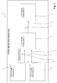
- Such a very simple FPGA model 1 is in the FIGS. 2 to 4 shown for different configurations.
- the method according to the invention begins with step S100, in which the FPGA model 1 is designed as an FPGA program by a user.
- the exemplary FPGA model 1 here comprises a plurality of components 3, which are distinguished here by the letters "A”, "B”, “C”, “D”.
- the FPGA model 1 further comprises a plurality of signal paths 5, which are arranged between the components 3.
- a marking 7 is set here in desired signal paths 5, as in FIG Fig. 2 is shown.
- the marker 7 is set in each signal path 5.
- the marked with the letter "C" component 3 is selected, and in all signal paths 5 of the component 3 markers 7 are automatically set.
- markers may be set individually on individually selected signal paths. Markers can be realized and visualized in different ways. For example, tags can have attributes of Be signals. A visualization can be done for example via a geometric or color highlighting the signal line. A visualization is not necessary in principle, but makes it easier to find the marked signals.
- a region 9 is graphically selected and set as a test focus. Accordingly, a mark 7 is set for all signal paths 5 which are located at least partially in the region 9.
- the graphic selection of the area 9 of the FPGA program takes place in a graphical development tool, not shown.
- the markers 7 are activated / deactivated. Accordingly, the markers 7 in this embodiment each have a switch which can be switched between the states “activated” and “deactivated” individually. A user manually activates / deactivates the tags 7 in the graphical developer tool.
- step S130 the tags 7 are configured.
- a user manually configures the tags 7 in the graphical developer tool, with one configuration selected for all tags 7 as a default.
- the default setting can be changed in any manner after the user has set the marker 7, for which purpose the user selects the configuration in a selection menu. In the FPGA model 1, only the set marker 7 is displayed as such, not your configuration, as in Fig. 2 seen.
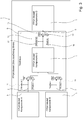
- the FPGA model 1 is generated as FPGA code based on at least a part of the model as a debug version.
- influencing structures 11 are inserted in the FPGA code at the active markings 9 in the signal path 5 provided with the respective marking 7, and the FPGA model 1 with the influencing structures 11 is generated.
- the respective signal path 5 with the set mark 7 is left unchanged.
- the influencing structures in the respective signal path 5 provided with the marking 7 are inserted as a function of the configuration of the marking 7.
- an influencing structure 11 for providing an alternative signal value in the signal path 5, for corrupting the signal value in the signal path 5, or for reading out a signal value in the marked signal path 5 is inserted.
- the influencing structures 11 can accordingly according to a first configuration, as in the embodiment in Fig. 3 shown, be designed. Accordingly, the Influencing structures 11 each have a multiplexer 13, here referred to as MUX on. In this case, the marked signal path 5 is connected to a first input 30 and an output 34 of the multiplexer 13, so that by default the marked signal path 5 is connected through the multiplexer 13. A second input 32 of the multiplexer 13 is connected to an alternative signal value, as explained below.
- the multiplexer 13 also has a selector input 15, referred to here as Sel, wherein the selector input 15 can be influenced during runtime of the FPGA code.
- About the selector input 15 of the multiplexer 13 can be switched at runtime dynamically, which is provided to the multiplexer 13 input signal on the marked signal path 5, ie whether the first input 30 or the second input 32 of the multiplexer 13 is connected to the output 34.
- the influencing structures 11 for those described with reference to FIGS Fig. 3 described configuration each one marked as a readback 17 influencing component, which allows a readback function, a readout of the signal value of the signal path 5 with the respective marker 7.
- the influencing component designated as readback 17 for reading out the signal value of the signal path 5 with the respective marking 7 is designed to establish a connection of the marked signal path 5 to an I / O pin. The connection of the marked signal path 5 with the I / O pin takes place directly or via a multiplexer.
- the influencing structures 11 include those referring to FIGS Fig. 3 Each configuration described a respective influencing component designated as Replace 19, by means of which a constant or a variable signal value is provided in the marked signal path 5 as an alternative signal value.
- the influencing component identified as Replace 19 is connected to the second input 32 of the multiplexer 13.
- the influencing structure 11 can have a memory element, for example a register, a look-up table (LUT) or a multiplexer, or can be connected to such a memory element in order to influence the signal value in the marked signal path 5 during runtime.
- LUT look-up table
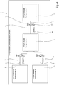
- the FPGA model 1 according to an alternative configuration of the markers 7 is shown in FIG Fig. 4 shown.
- the influencing structure 11 of this configuration which largely coincides with the In the first configuration, the influencing component identified as readback 17 is missing from the first configuration. Incidentally, the influencing structures 11 coincide.
- the FPGA model 1 according to an alternative configuration of the markers 7 is shown in FIG Fig. 5 shown in a detailed view.
- the influencing structure 11 has a distorting component 21 as an influencing component.
- the adulteration component 21 performs a change of a signal value applied in the marked signal path 5 using a parameter 23, designated here as Param, and provides this corrupted signal value at the multiplexer 13.
- signal values that can be influenced at runtime can thus be provided in the marked signal path 5.
- the FPGA model 1 is generated as FPGA code based on at least part of the model as a release. Accordingly, the FPGA code is generated to the FPGA model 1 without the interference patterns 11. Generation of the FPGA model 1 as FPGA code based on at least part of the model as a release occurs without changes to the FPGA program.
- the method described above opens up a large number of fields of application.
- the general debugging of internal FPGA components 3 at runtime should be mentioned, as for example with the general FPGA models and the configurations of the FIGS. 3 to 5 can be done.
- a debug option is activated at runtime of the FPGA model 1 by separating the marked signal paths 5 via the multiplexers 13 and providing desired signal values on the marked signal paths 5. The separation thus takes place via the selector input 15, via which between the first input 30 and the second input 32 of the respective multiplexer 13, the in Fig. 5 are shown, can be switched. This allows an internal simulation of error cases by replacing or corrupting the signal value originally applied to the signal path 5.
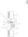
- HiL Another area of application in the field of automotive hardware-in-the-loop simulations (HiL) is the stimulation of I / O channels for testing external wiring (stimulus tests) on FPGA driven I / O channels, such as in Fig. 6 shown.
- a developer tool 40 which is embodied here as ControlDesk from the company dSPACE, is connected to a processor model 42 and above to the FPGA model 1.
- an internal HiL wiring 44 which implements the connection to a transfer connector 46.
- the control unit 60 is connected via a diagnostic connector, not shown, with a diagnostic tester 52.
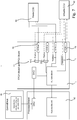
- FIG. 7 Another application example involves switching between a connection to a real and a virtual control unit (ECU) 60, 62, as described with reference to FIG Fig. 7 is described.
- the developer tool 40 is connected to a processor model 42 and above to the FPGA model 1.
- the real ECU 60 and the virtual ECU 62 Connected to the FPGA model 1 are the real ECU 60 and the virtual ECU 62.
- input channels 64 and output channels 66 are implemented separately.
- the influencing structures 11 can be switched between the connection to the real ECU 60 and the virtual ECU 62 for the input channels 64 and the output channels 66, respectively.
- the virtual ECU 62 can be calculated, for example, on the same compute node as the environment model.
- a virtual ECU can be connected to environment models retrospectively without recompilation. For this purpose, a synchronous switching of all multiplexers 13 takes place in operation between the virtual ECU 60 and the real ECU 62.
Landscapes
- Engineering & Computer Science (AREA)
- Theoretical Computer Science (AREA)
- Computer Hardware Design (AREA)
- Physics & Mathematics (AREA)
- General Engineering & Computer Science (AREA)
- General Physics & Mathematics (AREA)
- Evolutionary Computation (AREA)
- Geometry (AREA)
- Quality & Reliability (AREA)
- Software Systems (AREA)
- Logic Circuits (AREA)
- Tests Of Electronic Circuits (AREA)
Claims (14)
- Procédé pour contrôler le câblage externe des canaux E/S commandés par FPGA d'un simulateur HIL, dans lequel un outil de développeur (40) est relié avec un modèle de processeur (42) et, via ce dernier, avec un modèle FPGA (1), dans lequel un câble HIL interne (44) est reliée avec le modèle FPGA (1) via des ports E/S (54) du FPGA, qui réalise la liaison avec un connecteur de transfert (46), à la suite de quoi suit une liaison avec un faisceau de câbles externe (48) jusqu'à un appareil de commande (60), dans lequel l'appareil de commande (60) est relié avec un testeur de diagnostic (52) via un connecteur de diagnostic,
le procédé comprenant la création d'un code FPGA pour le modèle FPGA(1), la création d'un code FPGA comprenant les étapes suivantes ébaucher le modèle FPGA (1) en tant que programme FPGA avec au moins deux composantes (3) et au moins un trajet (5) de signal entre les au moins deux composantes (3),
définir un marquage (7) dans au moins un trajet (5) de signal dans le programme FPGA, et générer le modèle FPGA (1) en tant que code FPGA sur la base d'au moins une partie du modèle, sachant que l'étape de génération du modèle FPGA (1) en tant que code FPGA comprend l'insertion automatique d'une structure d'influence (11), laquelle peut lire et/ou modifier des valeurs de signal sur le trajet de signal, sur le trajet (5) de signal doté d'un marquage (7) et la création du modèle FPGA (1) avec la structure d'influence (11), sachant que l'étape d'insertion automatique d'une structure d'influence (11) comprend l'insertion d'un multiplexeur (13), qui peut être commuté pour la durée de fonctionnement pour fournir sur le trajet de signal marqué différents signaux d'entrée existant au multiplexeur,
le procédé comprenant en outre l'allocation de valeurs fixes pour les signaux existant au port E/S (54) d'un canal E/S commandé par FPGA via la structure d'influence (11) dans le modèle FPGA (1) et le contrôle de la conformité de la connexion de signal jusqu'au testeur de diagnostic (52). - Procédé selon la revendication 1, caractérisé en ce que
l'étape de définition d'un marquage (7) dans au moins un trajet (5) de signal dans le programme FPGA comprend la sélection d'une composante (3) du programme FPGA et la définition automatique de marquage (7) dans tous les trajets (5) de signaux de la composante (3) . - Procédé selon l'une des revendications 1 ou 2, caractérisé en ce que
l'étape de définition d'un marquage (7) dans au moins un trajet (5) de signal dans le programme FPGA comprend la sélection graphite d'une zone (9) du programme FPGA dans un outil de développeur graphique et la définition automatique de marquages (7) dans tous les trajets (5) de signaux dans la zone (9) de la sélection graphique. - Procédé selon l'une des revendications précédentes, caractérisé en ce que le procédé comprend, avant la génération du modèle FPGA (1), l'activation/la désactivation du marquage (7), et l'étape d'insertion automatique d'une structure d'influence (11) dans le trajet (5) de signal doté du marquage (7) comprend l'insertion automatique de la structure d'influence (11) pour les marquages actifs (7).
- Procédé selon l'une des revendications précédentes, caractérisé en ce que le procédé comprend, avant la génération du modèle FPGA (1), la configuration du marquage (7), et
l'étape d'insertion automatique d'une structure d'influence (11) dans le trajet (5) de signal doté du marquage (7) comprend l'insertion de la structure d'influence (11) en fonction de sa configuration. - Procédé selon l'une des revendications précédentes, caractérisé en ce que l'étape d'insertion automatique d'une structure d'influence (11) comprend l'insertion d'une structure d'influence (11) en vue de la fourniture d'une valeur de signal alternative dans le trajet de signal (5) ou de la mutilation de la valeur de signal dans le trajet (5) de signal.
- Procédé selon l'une des revendications précédentes, caractérisé en ce que l'étape d'insertion automatique d'une structure d'influence (11) comprend l'insertion d'une structure d'influence (11) en vue de la lecture d'une valeur de signal dans le trajet de signal (5).
- Procédé selon l'une des revendications précédentes, caractérisé en ce que l'étape d'insertion d'un multiplexeur (13) comprend l'insertion d'un multiplexeur (13) avec entrée (15) de sélecteur, dans lequel l'entrée (15) de sélecteur peut être influencée pour la durée de fonctionnement du code FPGA.
- Procédé selon l'une des revendications précédentes, caractérisé en ce que l'étape d'insertion automatique d'une structure d'influence (11) comprend l'insertion d'une structure d'influence (11) avec une valeur de signal pouvant être influencée pour la durée de fonctionnement.
- Procédé selon la revendication 9 précédente, caractérisé en ce que l'étape d'insertion d'une structure d'influence (11) avec une valeur de signal pouvant être influencé pour la durée de fonctionnement comprend l'insertion d'une composante d'influence FPGA (17, 19, 21) et la mise en connexion de la composante d'influence FPGA (17, 19, 21) insérée avec le trajet (5) de signal marqué.
- Procédé selon l'une des revendications précédentes, caractérisé en ce que le procédé comporte l'étape supplémentaire de création du modèle FPGA (1) en tant que code FPGA sur la base d'au moins une partie du modèle en tant que Release,
dans lequel l'étape de création du modèle FPGA (1) en tant que code FPGA en tant que Release comprend la création du modèle FPGA sans la structure d'influence (11). - Dispositif de traitement de données avec une unité de processeur, dans lequel le dispositif de traitement des données est réalisé pour exécuter le procédé selon l'une des revendications 1 à 11.
- Produit de programme informatique avec des instructions implémentées sur ordinateur, qui, après le chargement et le lancement dans un dispositif de traitement de données approprié, exécute les étapes du procédé selon l'une des revendications 1 à 11.
- Support de stockage numérique avec des signaux de commande lisibles électroniquement, qui peuvent coopérer avec un dispositif de traitement de données programmable de sorte que le procédé selon l'une des revendications 1 à 11 soit exécuté sur le dispositif de traitement de données.
Priority Applications (1)
| Application Number | Priority Date | Filing Date | Title |
|---|---|---|---|
| EP14177800.1A EP2977894B1 (fr) | 2014-07-21 | 2014-07-21 | Création d'un code FPGA ayant une structure d'influence automatiquement insérée |
Applications Claiming Priority (1)
| Application Number | Priority Date | Filing Date | Title |
|---|---|---|---|
| EP14177800.1A EP2977894B1 (fr) | 2014-07-21 | 2014-07-21 | Création d'un code FPGA ayant une structure d'influence automatiquement insérée |
Publications (2)
| Publication Number | Publication Date |
|---|---|
| EP2977894A1 EP2977894A1 (fr) | 2016-01-27 |
| EP2977894B1 true EP2977894B1 (fr) | 2018-09-12 |
Family
ID=51224741
Family Applications (1)
| Application Number | Title | Priority Date | Filing Date |
|---|---|---|---|
| EP14177800.1A Active EP2977894B1 (fr) | 2014-07-21 | 2014-07-21 | Création d'un code FPGA ayant une structure d'influence automatiquement insérée |
Country Status (1)
| Country | Link |
|---|---|
| EP (1) | EP2977894B1 (fr) |
Families Citing this family (1)
| Publication number | Priority date | Publication date | Assignee | Title |
|---|---|---|---|---|
| CN109739766B (zh) * | 2018-12-29 | 2022-04-29 | 湖北航天技术研究院总体设计所 | 一种快速搭建fpga数字仿真模型的系统及方法 |
Family Cites Families (3)
| Publication number | Priority date | Publication date | Assignee | Title |
|---|---|---|---|---|
| FR2873833B1 (fr) * | 2004-07-29 | 2006-10-13 | Temento Systems | Debogueur d'un circuit electronique fabrique a partir d'un programme en langage de description de materiel |
| US8261242B2 (en) * | 2008-06-09 | 2012-09-04 | International Business Machines Corporation | Assisting debug memory tracing using an instruction array that tracks the addresses of instructions modifying user specified objects |
| US20120005547A1 (en) * | 2010-06-30 | 2012-01-05 | Chang Chioumin M | Scalable system debugger for prototype debugging |
-
2014
- 2014-07-21 EP EP14177800.1A patent/EP2977894B1/fr active Active
Non-Patent Citations (1)
| Title |
|---|
| ANONYMOUS: "Field-programmable gate array - Wikipedia, the free encyclopedia", 4 February 2013 (2013-02-04), XP055123299, Retrieved from the Internet <URL:http://en.wikipedia.org/w/index.php?title=Field-programmable_gate_array&oldid=536512233> [retrieved on 20140613] * |
Also Published As
| Publication number | Publication date |
|---|---|
| EP2977894A1 (fr) | 2016-01-27 |
Similar Documents
| Publication | Publication Date | Title |
|---|---|---|
| DE3903835C2 (fr) | ||
| DE69826659T2 (de) | Billige, leicht anzuwendende software für ein automatisches testsystem | |
| EP1723513B1 (fr) | Procede pour configurer un programme informatique | |
| DE112016007220T5 (de) | Kontaktplanprogrammbearbeitungsunterstützungsvorrichtung und Kontaktplanprogrammbearbeitungsverfahren | |
| EP2990892B1 (fr) | Procédé de liaison d'une interface d'entrée/de sortie d'un appareil d'essai destiné à l'essai d'un appareil de commande | |
| DE10127170A1 (de) | Fehlersuchverfahren und Fehlersuchvorrichtung | |
| EP2799983B1 (fr) | Répartition flexible des canaux E/S d'un composant matériel | |
| DE3702408C2 (fr) | ||
| DE102006019292A1 (de) | Modellieren programmierbarer Einrichtungen | |
| DE10234135B4 (de) | Verfahren, System und Computerprogramm zum Steuern der Prüfung einer gedruckten Schaltungsplatine in Bezug auf Herstellungsdefekte | |
| DE102017211433A1 (de) | Verfahren zum Durchführen eines Funktionstests eines Steuergeräts in einem Hardware-in-the-Loop-Test, HIL-Test, sowie HIL-Prüfstand und Steuergerät | |
| DE102011009583B4 (de) | Einfaches Erzeugen einer Fernsteuersequenz für Messgeräte | |
| DE102017117496A1 (de) | Zell-Bewusste Fehlstellen-Charakterisierung und Wellenformanalyse mithilfe mehrerer Strobe-Punkte | |
| DE112021003677T5 (de) | Automatisierte unterstützte schaltkreisvalidierung | |
| EP3232327A1 (fr) | Procede d'essai d'un programme de commande d'un appareil de commande dans un environnement de simulation sur un ordinateur | |
| EP2343611A1 (fr) | Procédé de génération assistée par ordinateur d'un programme de commande exécutable et dispositif de configuration correspondant | |
| EP2977894B1 (fr) | Création d'un code FPGA ayant une structure d'influence automatiquement insérée | |
| DE10324594A1 (de) | Verfahren zum Bereitstellen einer verbesserten Simulationsfähigkeit eines dynamischen Systems außerhalb der ursprünglichen Modellierungsumgebung | |
| DE10213009A1 (de) | Verfahren zum elektronischen Testen von Speichermodulen | |
| DE2005884A1 (de) | Vorrichtung und Verfahren zur Feststellung von Fehlern in elektronischen Datenverarbeitungsanlagen | |
| DE10057575A1 (de) | Verfahren zur automatischen Softwaregenerierung | |
| DE102009019442A1 (de) | Testdatengenerator | |
| EP4010765A1 (fr) | Système et procédé de fourniture d'une simulation numérique d'une installation, et produit-programme d'ordinateur correspondant | |
| DE102008022132A1 (de) | Verfahren zum Konfigurieren einer Testeinrichtung, Testverfahren und Testeinrichtung | |
| EP2224340A1 (fr) | Procédé et système de gestion concus pour configurer un système d'information dynamique ainsi que produit programme d'ordinateur |
Legal Events
| Date | Code | Title | Description |
|---|---|---|---|
| PUAI | Public reference made under article 153(3) epc to a published international application that has entered the european phase |
Free format text: ORIGINAL CODE: 0009012 |
|
| AK | Designated contracting states |
Kind code of ref document: A1 Designated state(s): AL AT BE BG CH CY CZ DE DK EE ES FI FR GB GR HR HU IE IS IT LI LT LU LV MC MK MT NL NO PL PT RO RS SE SI SK SM TR |
|
| AX | Request for extension of the european patent |
Extension state: BA ME |
|
| 17P | Request for examination filed |
Effective date: 20160727 |
|
| RBV | Designated contracting states (corrected) |
Designated state(s): AL AT BE BG CH CY CZ DE DK EE ES FI FR GB GR HR HU IE IS IT LI LT LU LV MC MK MT NL NO PL PT RO RS SE SI SK SM TR |
|
| 17Q | First examination report despatched |
Effective date: 20160825 |
|
| STAA | Information on the status of an ep patent application or granted ep patent |
Free format text: STATUS: EXAMINATION IS IN PROGRESS |
|
| REG | Reference to a national code |
Ref country code: DE Ref legal event code: R079 Ref document number: 502014009432 Country of ref document: DE Free format text: PREVIOUS MAIN CLASS: G06F0009450000 Ipc: G06F0008410000 |
|
| GRAP | Despatch of communication of intention to grant a patent |
Free format text: ORIGINAL CODE: EPIDOSNIGR1 |
|
| STAA | Information on the status of an ep patent application or granted ep patent |
Free format text: STATUS: GRANT OF PATENT IS INTENDED |
|
| RIC1 | Information provided on ipc code assigned before grant |
Ipc: G06F 11/36 20060101ALI20180523BHEP Ipc: G06F 11/26 20060101ALI20180523BHEP Ipc: G06F 17/50 20060101ALI20180523BHEP Ipc: G06F 8/41 20180101AFI20180523BHEP |
|
| INTG | Intention to grant announced |
Effective date: 20180614 |
|
| GRAS | Grant fee paid |
Free format text: ORIGINAL CODE: EPIDOSNIGR3 |
|
| GRAA | (expected) grant |
Free format text: ORIGINAL CODE: 0009210 |
|
| STAA | Information on the status of an ep patent application or granted ep patent |
Free format text: STATUS: THE PATENT HAS BEEN GRANTED |
|
| AK | Designated contracting states |
Kind code of ref document: B1 Designated state(s): AL AT BE BG CH CY CZ DE DK EE ES FI FR GB GR HR HU IE IS IT LI LT LU LV MC MK MT NL NO PL PT RO RS SE SI SK SM TR |
|
| REG | Reference to a national code |
Ref country code: GB Ref legal event code: FG4D Free format text: NOT ENGLISH |
|
| REG | Reference to a national code |
Ref country code: CH Ref legal event code: EP |
|
| REG | Reference to a national code |
Ref country code: IE Ref legal event code: FG4D Free format text: LANGUAGE OF EP DOCUMENT: GERMAN |
|
| REG | Reference to a national code |
Ref country code: DE Ref legal event code: R096 Ref document number: 502014009432 Country of ref document: DE |
|
| REG | Reference to a national code |
Ref country code: AT Ref legal event code: REF Ref document number: 1041384 Country of ref document: AT Kind code of ref document: T Effective date: 20181015 |
|
| REG | Reference to a national code |
Ref country code: NL Ref legal event code: MP Effective date: 20180912 |
|
| REG | Reference to a national code |
Ref country code: LT Ref legal event code: MG4D |
|
| PG25 | Lapsed in a contracting state [announced via postgrant information from national office to epo] |
Ref country code: LT Free format text: LAPSE BECAUSE OF FAILURE TO SUBMIT A TRANSLATION OF THE DESCRIPTION OR TO PAY THE FEE WITHIN THE PRESCRIBED TIME-LIMIT Effective date: 20180912 Ref country code: SE Free format text: LAPSE BECAUSE OF FAILURE TO SUBMIT A TRANSLATION OF THE DESCRIPTION OR TO PAY THE FEE WITHIN THE PRESCRIBED TIME-LIMIT Effective date: 20180912 Ref country code: BG Free format text: LAPSE BECAUSE OF FAILURE TO SUBMIT A TRANSLATION OF THE DESCRIPTION OR TO PAY THE FEE WITHIN THE PRESCRIBED TIME-LIMIT Effective date: 20181212 Ref country code: GR Free format text: LAPSE BECAUSE OF FAILURE TO SUBMIT A TRANSLATION OF THE DESCRIPTION OR TO PAY THE FEE WITHIN THE PRESCRIBED TIME-LIMIT Effective date: 20181213 Ref country code: RS Free format text: LAPSE BECAUSE OF FAILURE TO SUBMIT A TRANSLATION OF THE DESCRIPTION OR TO PAY THE FEE WITHIN THE PRESCRIBED TIME-LIMIT Effective date: 20180912 Ref country code: NO Free format text: LAPSE BECAUSE OF FAILURE TO SUBMIT A TRANSLATION OF THE DESCRIPTION OR TO PAY THE FEE WITHIN THE PRESCRIBED TIME-LIMIT Effective date: 20181212 Ref country code: FI Free format text: LAPSE BECAUSE OF FAILURE TO SUBMIT A TRANSLATION OF THE DESCRIPTION OR TO PAY THE FEE WITHIN THE PRESCRIBED TIME-LIMIT Effective date: 20180912 |
|
| PG25 | Lapsed in a contracting state [announced via postgrant information from national office to epo] |
Ref country code: LV Free format text: LAPSE BECAUSE OF FAILURE TO SUBMIT A TRANSLATION OF THE DESCRIPTION OR TO PAY THE FEE WITHIN THE PRESCRIBED TIME-LIMIT Effective date: 20180912 Ref country code: AL Free format text: LAPSE BECAUSE OF FAILURE TO SUBMIT A TRANSLATION OF THE DESCRIPTION OR TO PAY THE FEE WITHIN THE PRESCRIBED TIME-LIMIT Effective date: 20180912 Ref country code: HR Free format text: LAPSE BECAUSE OF FAILURE TO SUBMIT A TRANSLATION OF THE DESCRIPTION OR TO PAY THE FEE WITHIN THE PRESCRIBED TIME-LIMIT Effective date: 20180912 |
|
| PG25 | Lapsed in a contracting state [announced via postgrant information from national office to epo] |
Ref country code: ES Free format text: LAPSE BECAUSE OF FAILURE TO SUBMIT A TRANSLATION OF THE DESCRIPTION OR TO PAY THE FEE WITHIN THE PRESCRIBED TIME-LIMIT Effective date: 20180912 Ref country code: IS Free format text: LAPSE BECAUSE OF FAILURE TO SUBMIT A TRANSLATION OF THE DESCRIPTION OR TO PAY THE FEE WITHIN THE PRESCRIBED TIME-LIMIT Effective date: 20190112 Ref country code: IT Free format text: LAPSE BECAUSE OF FAILURE TO SUBMIT A TRANSLATION OF THE DESCRIPTION OR TO PAY THE FEE WITHIN THE PRESCRIBED TIME-LIMIT Effective date: 20180912 Ref country code: EE Free format text: LAPSE BECAUSE OF FAILURE TO SUBMIT A TRANSLATION OF THE DESCRIPTION OR TO PAY THE FEE WITHIN THE PRESCRIBED TIME-LIMIT Effective date: 20180912 Ref country code: PL Free format text: LAPSE BECAUSE OF FAILURE TO SUBMIT A TRANSLATION OF THE DESCRIPTION OR TO PAY THE FEE WITHIN THE PRESCRIBED TIME-LIMIT Effective date: 20180912 Ref country code: CZ Free format text: LAPSE BECAUSE OF FAILURE TO SUBMIT A TRANSLATION OF THE DESCRIPTION OR TO PAY THE FEE WITHIN THE PRESCRIBED TIME-LIMIT Effective date: 20180912 Ref country code: RO Free format text: LAPSE BECAUSE OF FAILURE TO SUBMIT A TRANSLATION OF THE DESCRIPTION OR TO PAY THE FEE WITHIN THE PRESCRIBED TIME-LIMIT Effective date: 20180912 Ref country code: NL Free format text: LAPSE BECAUSE OF FAILURE TO SUBMIT A TRANSLATION OF THE DESCRIPTION OR TO PAY THE FEE WITHIN THE PRESCRIBED TIME-LIMIT Effective date: 20180912 |
|
| PG25 | Lapsed in a contracting state [announced via postgrant information from national office to epo] |
Ref country code: SM Free format text: LAPSE BECAUSE OF FAILURE TO SUBMIT A TRANSLATION OF THE DESCRIPTION OR TO PAY THE FEE WITHIN THE PRESCRIBED TIME-LIMIT Effective date: 20180912 Ref country code: PT Free format text: LAPSE BECAUSE OF FAILURE TO SUBMIT A TRANSLATION OF THE DESCRIPTION OR TO PAY THE FEE WITHIN THE PRESCRIBED TIME-LIMIT Effective date: 20190112 Ref country code: SK Free format text: LAPSE BECAUSE OF FAILURE TO SUBMIT A TRANSLATION OF THE DESCRIPTION OR TO PAY THE FEE WITHIN THE PRESCRIBED TIME-LIMIT Effective date: 20180912 |
|
| REG | Reference to a national code |
Ref country code: DE Ref legal event code: R097 Ref document number: 502014009432 Country of ref document: DE |
|
| PLBE | No opposition filed within time limit |
Free format text: ORIGINAL CODE: 0009261 |
|
| STAA | Information on the status of an ep patent application or granted ep patent |
Free format text: STATUS: NO OPPOSITION FILED WITHIN TIME LIMIT |
|
| PG25 | Lapsed in a contracting state [announced via postgrant information from national office to epo] |
Ref country code: DK Free format text: LAPSE BECAUSE OF FAILURE TO SUBMIT A TRANSLATION OF THE DESCRIPTION OR TO PAY THE FEE WITHIN THE PRESCRIBED TIME-LIMIT Effective date: 20180912 |
|
| 26N | No opposition filed |
Effective date: 20190613 |
|
| PG25 | Lapsed in a contracting state [announced via postgrant information from national office to epo] |
Ref country code: SI Free format text: LAPSE BECAUSE OF FAILURE TO SUBMIT A TRANSLATION OF THE DESCRIPTION OR TO PAY THE FEE WITHIN THE PRESCRIBED TIME-LIMIT Effective date: 20180912 |
|
| PG25 | Lapsed in a contracting state [announced via postgrant information from national office to epo] |
Ref country code: MC Free format text: LAPSE BECAUSE OF FAILURE TO SUBMIT A TRANSLATION OF THE DESCRIPTION OR TO PAY THE FEE WITHIN THE PRESCRIBED TIME-LIMIT Effective date: 20180912 |
|
| REG | Reference to a national code |
Ref country code: CH Ref legal event code: PL |
|
| PG25 | Lapsed in a contracting state [announced via postgrant information from national office to epo] |
Ref country code: TR Free format text: LAPSE BECAUSE OF FAILURE TO SUBMIT A TRANSLATION OF THE DESCRIPTION OR TO PAY THE FEE WITHIN THE PRESCRIBED TIME-LIMIT Effective date: 20180912 |
|
| REG | Reference to a national code |
Ref country code: BE Ref legal event code: MM Effective date: 20190731 |
|
| PG25 | Lapsed in a contracting state [announced via postgrant information from national office to epo] |
Ref country code: LI Free format text: LAPSE BECAUSE OF NON-PAYMENT OF DUE FEES Effective date: 20190731 Ref country code: CH Free format text: LAPSE BECAUSE OF NON-PAYMENT OF DUE FEES Effective date: 20190731 Ref country code: LU Free format text: LAPSE BECAUSE OF NON-PAYMENT OF DUE FEES Effective date: 20190721 Ref country code: BE Free format text: LAPSE BECAUSE OF NON-PAYMENT OF DUE FEES Effective date: 20190731 |
|
| PG25 | Lapsed in a contracting state [announced via postgrant information from national office to epo] |
Ref country code: FR Free format text: LAPSE BECAUSE OF NON-PAYMENT OF DUE FEES Effective date: 20190731 |
|
| PG25 | Lapsed in a contracting state [announced via postgrant information from national office to epo] |
Ref country code: IE Free format text: LAPSE BECAUSE OF NON-PAYMENT OF DUE FEES Effective date: 20190721 |
|
| REG | Reference to a national code |
Ref country code: AT Ref legal event code: MM01 Ref document number: 1041384 Country of ref document: AT Kind code of ref document: T Effective date: 20190721 |
|
| PG25 | Lapsed in a contracting state [announced via postgrant information from national office to epo] |
Ref country code: AT Free format text: LAPSE BECAUSE OF NON-PAYMENT OF DUE FEES Effective date: 20190721 |
|
| PG25 | Lapsed in a contracting state [announced via postgrant information from national office to epo] |
Ref country code: CY Free format text: LAPSE BECAUSE OF FAILURE TO SUBMIT A TRANSLATION OF THE DESCRIPTION OR TO PAY THE FEE WITHIN THE PRESCRIBED TIME-LIMIT Effective date: 20180912 |
|
| PG25 | Lapsed in a contracting state [announced via postgrant information from national office to epo] |
Ref country code: MT Free format text: LAPSE BECAUSE OF FAILURE TO SUBMIT A TRANSLATION OF THE DESCRIPTION OR TO PAY THE FEE WITHIN THE PRESCRIBED TIME-LIMIT Effective date: 20180912 Ref country code: HU Free format text: LAPSE BECAUSE OF FAILURE TO SUBMIT A TRANSLATION OF THE DESCRIPTION OR TO PAY THE FEE WITHIN THE PRESCRIBED TIME-LIMIT; INVALID AB INITIO Effective date: 20140721 |
|
| REG | Reference to a national code |
Ref country code: DE Ref legal event code: R081 Ref document number: 502014009432 Country of ref document: DE Owner name: DSPACE GMBH, DE Free format text: FORMER OWNER: DSPACE DIGITAL SIGNAL PROCESSING AND CONTROL ENGINEERING GMBH, 33102 PADERBORN, DE |
|
| PG25 | Lapsed in a contracting state [announced via postgrant information from national office to epo] |
Ref country code: MK Free format text: LAPSE BECAUSE OF FAILURE TO SUBMIT A TRANSLATION OF THE DESCRIPTION OR TO PAY THE FEE WITHIN THE PRESCRIBED TIME-LIMIT Effective date: 20180912 |
|
| P01 | Opt-out of the competence of the unified patent court (upc) registered |
Effective date: 20230517 |
|
| PGFP | Annual fee paid to national office [announced via postgrant information from national office to epo] |
Ref country code: GB Payment date: 20230720 Year of fee payment: 10 |
|
| PGFP | Annual fee paid to national office [announced via postgrant information from national office to epo] |
Ref country code: DE Payment date: 20230719 Year of fee payment: 10 |