EP2977795A1 - Curved diffraction grating, production method therefor, and optical device - Google Patents
Curved diffraction grating, production method therefor, and optical device Download PDFInfo
- Publication number
- EP2977795A1 EP2977795A1 EP14770190.8A EP14770190A EP2977795A1 EP 2977795 A1 EP2977795 A1 EP 2977795A1 EP 14770190 A EP14770190 A EP 14770190A EP 2977795 A1 EP2977795 A1 EP 2977795A1
- Authority
- EP
- European Patent Office
- Prior art keywords
- substrate
- curved
- grating
- amorphous material
- diffraction grating
- Prior art date
- Legal status (The legal status is an assumption and is not a legal conclusion. Google has not performed a legal analysis and makes no representation as to the accuracy of the status listed.)
- Granted
Links
Images



Classifications
-
- G—PHYSICS
- G02—OPTICS
- G02B—OPTICAL ELEMENTS, SYSTEMS OR APPARATUS
- G02B5/00—Optical elements other than lenses
- G02B5/18—Diffraction gratings
- G02B5/1847—Manufacturing methods
- G02B5/1852—Manufacturing methods using mechanical means, e.g. ruling with diamond tool, moulding
-
- B—PERFORMING OPERATIONS; TRANSPORTING
- B29—WORKING OF PLASTICS; WORKING OF SUBSTANCES IN A PLASTIC STATE IN GENERAL
- B29C—SHAPING OR JOINING OF PLASTICS; SHAPING OF MATERIAL IN A PLASTIC STATE, NOT OTHERWISE PROVIDED FOR; AFTER-TREATMENT OF THE SHAPED PRODUCTS, e.g. REPAIRING
- B29C59/00—Surface shaping of articles, e.g. embossing; Apparatus therefor
- B29C59/02—Surface shaping of articles, e.g. embossing; Apparatus therefor by mechanical means, e.g. pressing
- B29C59/026—Surface shaping of articles, e.g. embossing; Apparatus therefor by mechanical means, e.g. pressing of layered or coated substantially flat surfaces
-
- B—PERFORMING OPERATIONS; TRANSPORTING
- B29—WORKING OF PLASTICS; WORKING OF SUBSTANCES IN A PLASTIC STATE IN GENERAL
- B29C—SHAPING OR JOINING OF PLASTICS; SHAPING OF MATERIAL IN A PLASTIC STATE, NOT OTHERWISE PROVIDED FOR; AFTER-TREATMENT OF THE SHAPED PRODUCTS, e.g. REPAIRING
- B29C59/00—Surface shaping of articles, e.g. embossing; Apparatus therefor
- B29C59/02—Surface shaping of articles, e.g. embossing; Apparatus therefor by mechanical means, e.g. pressing
- B29C59/021—Surface shaping of articles, e.g. embossing; Apparatus therefor by mechanical means, e.g. pressing of profiled articles, e.g. hollow or tubular articles, beams
-
- B—PERFORMING OPERATIONS; TRANSPORTING
- B29—WORKING OF PLASTICS; WORKING OF SUBSTANCES IN A PLASTIC STATE IN GENERAL
- B29D—PRODUCING PARTICULAR ARTICLES FROM PLASTICS OR FROM SUBSTANCES IN A PLASTIC STATE
- B29D11/00—Producing optical elements, e.g. lenses or prisms
- B29D11/00009—Production of simple or compound lenses
- B29D11/0048—Moulds for lenses
-
- B—PERFORMING OPERATIONS; TRANSPORTING
- B29—WORKING OF PLASTICS; WORKING OF SUBSTANCES IN A PLASTIC STATE IN GENERAL
- B29D—PRODUCING PARTICULAR ARTICLES FROM PLASTICS OR FROM SUBSTANCES IN A PLASTIC STATE
- B29D11/00—Producing optical elements, e.g. lenses or prisms
- B29D11/0074—Production of other optical elements not provided for in B29D11/00009- B29D11/0073
- B29D11/00769—Producing diffraction gratings
-
- G—PHYSICS
- G01—MEASURING; TESTING
- G01N—INVESTIGATING OR ANALYSING MATERIALS BY DETERMINING THEIR CHEMICAL OR PHYSICAL PROPERTIES
- G01N21/00—Investigating or analysing materials by the use of optical means, i.e. using sub-millimetre waves, infrared, visible or ultraviolet light
- G01N21/17—Systems in which incident light is modified in accordance with the properties of the material investigated
- G01N21/25—Colour; Spectral properties, i.e. comparison of effect of material on the light at two or more different wavelengths or wavelength bands
- G01N21/31—Investigating relative effect of material at wavelengths characteristic of specific elements or molecules, e.g. atomic absorption spectrometry
-
- G—PHYSICS
- G02—OPTICS
- G02B—OPTICAL ELEMENTS, SYSTEMS OR APPARATUS
- G02B1/00—Optical elements characterised by the material of which they are made; Optical coatings for optical elements
- G02B1/04—Optical elements characterised by the material of which they are made; Optical coatings for optical elements made of organic materials, e.g. plastics
-
- G—PHYSICS
- G02—OPTICS
- G02B—OPTICAL ELEMENTS, SYSTEMS OR APPARATUS
- G02B5/00—Optical elements other than lenses
- G02B5/18—Diffraction gratings
- G02B5/1814—Diffraction gratings structurally combined with one or more further optical elements, e.g. lenses, mirrors, prisms or other diffraction gratings
-
- G—PHYSICS
- G02—OPTICS
- G02B—OPTICAL ELEMENTS, SYSTEMS OR APPARATUS
- G02B5/00—Optical elements other than lenses
- G02B5/18—Diffraction gratings
- G02B5/1847—Manufacturing methods
- G02B5/1857—Manufacturing methods using exposure or etching means, e.g. holography, photolithography, exposure to electron or ion beams
-
- G—PHYSICS
- G02—OPTICS
- G02B—OPTICAL ELEMENTS, SYSTEMS OR APPARATUS
- G02B5/00—Optical elements other than lenses
- G02B5/18—Diffraction gratings
- G02B5/1861—Reflection gratings characterised by their structure, e.g. step profile, contours of substrate or grooves, pitch variations, materials
-
- B—PERFORMING OPERATIONS; TRANSPORTING
- B29—WORKING OF PLASTICS; WORKING OF SUBSTANCES IN A PLASTIC STATE IN GENERAL
- B29C—SHAPING OR JOINING OF PLASTICS; SHAPING OF MATERIAL IN A PLASTIC STATE, NOT OTHERWISE PROVIDED FOR; AFTER-TREATMENT OF THE SHAPED PRODUCTS, e.g. REPAIRING
- B29C59/00—Surface shaping of articles, e.g. embossing; Apparatus therefor
- B29C59/02—Surface shaping of articles, e.g. embossing; Apparatus therefor by mechanical means, e.g. pressing
- B29C59/022—Surface shaping of articles, e.g. embossing; Apparatus therefor by mechanical means, e.g. pressing characterised by the disposition or the configuration, e.g. dimensions, of the embossments or the shaping tools therefor
- B29C2059/023—Microembossing
Definitions
- the present invention relates to a curved grating, a method for manufacturing the same, and an optical device, and particularly to a curved grating which spectrally splits and converges light, and an optical device using the same.
- a curved grating which is an optical element of a spectrophotometer, has both capabilities of spectrally splitting and converging light. Therefore, the number of components can be reduced and the configuration of the device can be simplified.
- a curved grating is manufactured by preparing a mold of a diffraction grating by a method in which a curved substrate is carved with a machine such as a ruling engine, and then transferring the carved pattern to a resin, metal or the like.
- WO2008/081555 discloses a method in which a flat grating and a concave blazed grating are prepared, using semiconductor photolithography and etching processes.
- a diffraction grating pattern is formed on a flexible material such as a resin or thin metal film, which is then attached to a substrate curved to a predetermined curvature, thus forming a mold.
- This mold is brought in contact with a liquid curved grating material before hardening, and the material is hardened to prepare a curved grating.
- JP-A-8-29610 (PTL 3), a replica layer (diffraction grating part) using a reactive curing resin is stacked on a flexible substrate, and the flat grating is curved, utilizing the curing contraction of the reactive curing resin.
- a flat grating substrate is transferred to a flexible material such as a silicone resin, which is then fixed to a curved substrate, thus forming a curved grating mold.
- JP-A-2010-25723 discloses an X-ray reflection device having an X-ray reflector which is prepared by heating a silicon substrate to a high temperature in a hydrogen atmosphere so as to plastically deform the silicon substrate into a desired shape, and then stacking a number of the same substrates.
- an object of the invention is to provide a technique which enables preparation of a curved grating having a desired curvature, by plastically deforming, along a curved substrate, a flat grating prepared by a semiconductor process on a silicon substrate, and which thus prepares a diffraction grating with high accuracy.
- the invention has the following characteristics.
- a diffraction grating pattern is formed on a silicon substrate, and the diffraction grating pattern is transferred to an amorphous material, thus preparing a flat grating made of the amorphous material.
- This flat grating made of the amorphous material is deformed into a curved surface and mounted on a curved fixed substrate, thus preparing a curved grating mold.
- This curved grating mold is transferred to a metal film or resin, thus preparing a curved grating.
- the amorphous material a glass, metal or the like is used.
- thermal deformation of the amorphous material substrate plastic deformation by application of a load, electroplating with a metal or the like is used.
- thermal deformation or plastic deformation thermal deformation or plastic deformation is used after the silicon flat grating and the amorphous material substrate are bonded together in order to improve the transfer accuracy of the diffraction grating pattern.
- the void formed between these can be restrained.
- the void can also be restrained by forming a vent groove in the silicon diffraction grating to the outside of the substrate corresponding to the diffraction grating pattern. If the vent groove is removed after the diffraction grating pattern is transferred to the amorphous material substrate, diffracted light will not be affected at the time of transfer to the curved grating. Also, the diffraction grating pattern may be used as a vent groove.
- the thermal deformation of the mold is slight at the time of pattern transfer to the curved grating and therefore accuracy can be improved, and release from the mold can be achieved without having deformation due to the pulling at the time of release and therefore the life of the mold is improved.
- anodic bonding, direct bonding, or eutectic bonding is used as a method for mounting the amorphous material substrate on the curved fixed substrate after the amorphous material substrate with the diffraction grating pattern transferred thereto is deformed into a curved surface.
- a glass is used as the amorphous material
- a curved grating mold can be formed by anodic bonding using silicon as the curved fixed substrate.
- direct bonding the deformation and the bonding with the curved fixed substrate can be prepared in the same process.
- direct bonding if the linear expansion coefficients of the amorphous material substrate and the curved fixed substrate are greatly different in the high-temperature atmosphere, damage occurs due to thermal contraction difference in the cooling process.
- the curved grating mold can be prepared with good surface accuracy.
- the curved grating mold may be prepared using eutectic bonding, by preparing a solder on the bonding surface between the amorphous material substrate and the curved fixed substrate by sputtering, deposition, electroplating or the like.
- the curved grating mold prepared by the above method is transferred to a resin, metal or the like, thus preparing a curved grating.
- a curved grating having a desired curvature can be prepared by plastically deforming, along a curved substrate, a flat grating prepared by a semiconductor process on a silicon substrate. Since the silicon diffraction grating pattern can be used as it is, a highly accurate diffraction grating can be prepared.
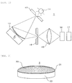
- FIG. 1 is a schematic view showing an example of a spectrophotometer using a curved grating of the invention.
- a spectrophotometer 1 is used for measurement of concentration and identification of a substance, by selectively absorbing light with a wavelength unique to a chemical bond of a substance such as a chemical substance or biological substance.
- a spectrophotometer 1 includes a light source 11, slits 12, 14, a diffraction grating 13, a light condensing element 15, and a detector 17.
- the light cast from the light source 11 is cast on the diffraction grating 13 via the slit 12 and spectrally split by the diffraction grating 13.
- the spectrally split light becomes incident on a sample 16 via the slit 14 and the light condensing element 15, and the detector 17 measures the absorption (damping) of the wavelength.
- the diffraction grating 13 is rotated to cast light with a specific wavelength on the sample 16.
- the optical elements such as the mirror and light condensing element in the spectrophotometer 1 can be simplified.
- a curved grating may be a spherical grating or toroidal grating. The specific shape thereof will be described.
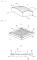
- FIG. 2 shows a mold of a spherical grating.
- a spherical grating is a diffraction grating having a spherical surface with a uniform curvature in any axial direction.
- a curved grating mold 2 is made up of an amorphous material substrate 21 with a diffraction grating pattern 20 formed thereon, and a curved fixed substrate 22.
- the amorphous material substrate 21 and the curved fixed substrate 22 are fixed together by a connection method chosen from direct bonding, anodic bonding, eutectic bonding, resin bonding or the like.
- FIG. 3 shows a mold of a toroidal grating.
- a toroidal grating is a diffraction grating having a toroidal surface with different curvatures in different axial directions, unlike a spherical grating.
- the toroidal grating has different curvatures in direction A-A and direction B-B in the illustration.
- a curved grating mold 2 is made up of an amorphous material substrate 21 with a diffraction grating pattern 20 formed thereon, and a curved fixed substrate 22. Since the amorphous material substrate 21 is plastically deformed along the curved fixed substrate 22, mounting on a toroidal surface with different curvatures in different axial directions is possible.
- the amorphous material substrate 21 and the curved fixed substrate 22 are fixed together by a connection method chosen from direct bonding, anodic bonding, eutectic bonding, resin bonding or the like.
- a connection method chosen from direct bonding, anodic bonding, eutectic bonding, resin bonding or the like.
- the following methods can be used as methods for manufacturing a curved grating represented by the above spherical grating or toroidal grating.
- FIG. 4 is a view showing an example of a silicon diffraction grating substrate of the invention.
- FIG. 4(a) is a bird's-eye view of the silicon diffraction grating substrate.
- a diffraction grating pattern 20 is formed by a semiconductor process (for example, a process such as photolithography or etching).
- a vent groove 32 is formed at a site that does not affect the spectral splitting by the diffraction grating pattern 20.
- This vent groove 32 is for releasing air bubbles at the time of transfer to an amorphous material substrate 21, and is installed at an outer peripheral part of an area 31 (dashed line) where the amorphous material substrate 21 is deformed into a curved grating.
- the diffraction grating pattern 20 can be formed to the outer peripheral part of the silicon substrate 3 and used instead of the vent groove 32.
- metal glass or the like can be used as well as glass.
- a manufacturing method in which a film is formed by deposition, sputtering, electroplating or the like and then the silicon is removed is employed instead of bonding transfer as in the case of glass.
- metal glass can be formed into a film by deposition, sputtering, electroplating or the like, a diffraction grating pattern can be formed.
- the metal glass may include Zr-Cu-Al-Ni, Pd-Ni-P and the like.
- FIG. 4 (b) is a view showing a cross-sectional view taken along direction A-A when the silicon flat grating 3 is rotated 180 degrees and turned upside down.
- the diffraction grating pattern 20 has the peripheral parts thereof supported by a support plate 50.
- a convex part of a curved substrate 26 made up of the amorphous material substrate 21, described below, is abutted and pressed against the surface where the diffraction grating pattern 20 is not formed (area indicated by the circular dashed line 31 in FIG. 4(a) ), thus curving the diffraction grating pattern 20. Details thereof will be described below.
- Examples 1 to 3 described below are examples in which a curved grating mold 2 is prepared by forming a diffraction grating pattern by transfer using a silicon substrate.
- Example 4 is an example in which a curved grating mold 2 is prepared by forming a diffraction grating pattern without using a silicon substrate.
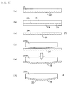
- Example 1 The method for manufacturing a curved grating mold 2 in Example 1 will be described using FIG. 5 .
- a diffraction grating pattern 30 having a waved shape is formed on a bulk silicon substrate 3 by a semiconductor process (for example, photolithography or etching) ( FIG. 5(a) ).
- the silicon substrate is bonded to a glass substrate 24 and heated to around the softening point.
- the shape similar to the diffraction grating pattern 30 formed on the silicon substrate 3 is transferred to the glass substrate 24, forming a diffraction grating pattern 20 ( FIG. 5(b) ).
- the silicon substrate 3 is removed by etching, thus preparing a glass diffraction grating 25 ( FIG. 5(c) ).
- a desired curved substrate 26 is installed on the back side of the surface where the diffraction grating pattern 20 is formed, of the glass diffraction grating 25 ( FIG. 5(d) ). At this point, though not shown in this illustration, the support plate 50 of the diffraction grating pattern 20 is prepared in the state of FIG. 4(b) .
- the glass diffraction grating 25 is deformed ( FIG. 5(e) ).
- the curved substrate 26 is detached and a silicon curved fixed substrate 22a installed.
- the glass diffraction grating 25 and the silicon curved fixed substrate 22a are anodic-bonded ( FIG. 5(f) ).
- the curved fixed substrate 22a and the glass diffraction grating 25 are both used as electrodes and a current is applied between the two electrodes, thus bonding the two together.
- the silicon substrate 3 and the glass substrate 24 are bonded together to transfer the diffraction grating pattern 30, there is no misalignment between the substrates and the diffraction grating pattern 30 can be transferred with high accuracy.
- a diffraction grating pattern 30 having a waved shape is formed on a bulk silicon substrate 3 by a semiconductor process (for example, photolithography or etching) ( FIG. 6(a) ).
- the silicon substrate is bonded to a glass substrate 24 and heated to around the softening point.
- the shape similar to the diffraction grating pattern 30 formed on the silicon substrate 3 is transferred to the glass substrate 24, forming a diffraction grating pattern 20 ( FIG. 6(b) ).
- the silicon substrate 3 is removed by etching, thus preparing a glass flat grating 25 ( FIG. 6(c) ).
- a desired glass curved fixed substrate 22b is installed on the back side of the surface where the diffraction grating pattern 20 is formed, of the glass diffraction grating 25 ( FIG. 6(d) ).
- the support plate 50 of the diffraction grating pattern 20 is prepared in the state of FIG. 4(b) .
- the glass diffraction grating 25 is deformed ( FIG. 6(e) ).
- the glass diffraction grating 25 and the glass curved fixed substrate 22b can be fixed together by heat.
- the glass diffraction grating 25 is deformed and fixed to the curved fixed substrate 22b from a center part and therefore can be fixed without a void.
- an unnecessary part of the glass diffraction grating 25 is removed, forming a curved grating mold 2 ( FIG. 6(f) ).
- a characteristic of this example is that, since the glass curved fixed substrate 22b is used, which has the same linear expansion coefficient as the glass flat grating 25, damage at the time of cooling from the high temperature can be prevented.
- a diffraction grating pattern 30 having a waved shape is formed on a bulk silicon substrate 3 by a semiconductor process (for example, photolithography or etching) ( FIG. 7(a) ).
- the silicon substrate is bonded to a glass substrate 24 and heated to around the softening point.
- the shape similar to the diffraction grating pattern 30 formed on the silicon substrate 3 is transferred to the glass substrate 24, forming a diffraction grating pattern 20 on the glass substrate 24 ( FIG. 7(b) ).
- the silicon substrate 3 is formed into a thin film by grinding or etching ( FIG. 7(c) ).
- a desired glass curved fixed substrate 22b is installed on the back side of the surface where the diffraction grating pattern 20 is formed, of the glass diffraction grating 25, and a concave curved substrate 26 having a symmetrical shape to the curved fixed substrate 22b is installed on the silicon substrate 3 side ( FIG. 7(d) ).
- the glass diffraction grating 25 is deformed ( FIG. 7(e) ).
- the glass diffraction grating 25 and the glass curved fixed substrate 22b can be fixed together by heat.
- the glass diffraction grating 25 is deformed and fixed to the curved fixed substrate 22b from a center part and therefore can be fixed without a void.
- an unnecessary part of the glass diffraction grating 25 is removed by etching the silicon substrate 3, forming a curved grating mold 2 ( FIG. 7(f) ).
- a characteristic of this example is that, since the diffraction grating patterns 20, 30 do not contact the curved fixed substrate 22b and the concave curved substrate 26, the glass diffraction grating 25 can be formed into a desired curved shape with high accuracy.
- the curved fixed substrate 22b and the concave curved substrate 26 are installed and a high temperature at which the glass shows viscoelasticity is applied.
- a diffraction grating pattern 30 is formed on a bulk silicon substrate 3 by a semiconductor process (for example, photolithography or etching) ( FIG. 8(a) ).
- the silicon substrate is bonded to a glass substrate 24 and heated to around the softening point, thus forming a diffraction grating pattern 20 on the glass substrate 24 ( FIG. 8(b) ).
- the silicon substrate 3 is removed by grinding or etching ( FIG. 8(c) ).
- a material which is highly temperature-resistant and hard to deform such as silicon or tungsten, is formed into a film as a protection film 33 by sputtering ( FIG. 8(d) ).
- a desired glass curved fixed substrate 22b is installed on the back side of the surface where the diffraction grating pattern 20 is formed, of the glass diffraction grating 25, and a concave curved substrate 26 having a symmetrical shape to the curved fixed substrate 22b is installed on the protection film 33 side ( FIG. 8(e) ).
- the glass diffraction grating 25 is deformed ( FIG. 8(f) ).
- the glass flat grating 25 and the glass curved fixed substrate 22b can be fixed together by heat.
- the diffraction grating pattern 20 is protected by the projection film 33 and therefore is relatively less subject to damage from the concave curved substrate 26.
- the glass diffraction grating 25 is deformed and fixed to the curved fixed substrate 22b from a center part and therefore can be fixed without a void.
- the concave curved substrate 26 is removed ( FIG. 8(g) ) and the protection film 33 is removed by etching ( FIG. 8(h) ).
- a characteristic of this example is that the projection film 33 is a thin film and that the glass diffraction grating 25 can be formed into a desired curved shape with high accuracy.
- Example 5 the method for manufacturing a curved grating mold 2 in Example 5 will be described using FIG. 9 .
- This example is different from the above Examples 1 to 3 in that the processes such as the formation of a diffraction grating pattern on a silicon substrate and the transfer of the diffraction grating pattern to a glass substrate are not used.
- a diffraction grating pattern 20 is formed on a bulk glass substrate 24 by a semiconductor process (for example, photolithography or etching), thus forming a glass diffraction grating 25 ( FIG. 9(a) ).
- a desired glass curved fixed substrate 22 is installed on the back side of the surface where the diffraction grating pattern 20 is formed, of the glass diffraction grating 25 ( FIG. 9(b) ).
- the support plate 50 of the diffraction grating pattern 20 is prepared in the state of FIG. 4(b) .
- the glass diffraction grating 25 is deformed ( FIG. 9(c) ). At this point, the glass diffraction grating 25 and the glass curved fixed substrate 22 can be fixed together by heat. The glass diffraction grating 25 is deformed and fixed to the curved fixed substrate 22 from a center part and therefore can be fixed without a void.
- a characteristic of this example is that, since the glass diffraction grating 25 is worked by a semiconductor process (for example, photolithography or etching), the processes of forming a diffraction grating pattern on a silicon substrate, bonding to a glass substrate, and transfer, described in Examples 1 to 3, can be omitted.
- a semiconductor process for example, photolithography or etching
- the curved grating mold 2 formed by one of the methods described in Example 1 to 5 is prepared ( FIG. 10(a) ).
- a release layer is formed on the surface of the curved grating mold 2 and a reflection film 41 is formed on the release layer ( FIG. 10(b) ).
- the release laser is provided to facilitate release when detaching a resin 42 and a fixed substrate 43 from the curved grating mold 2, described below using FIG. 10(d) .
- a liquid curing resin 42 and a fixed substrate 43 are installed on the reflection film 41 ( FIG. 10(c) ).
- the resin 42 and the fixed substrate 43 are detached from the curved grating mold 2, thus manufacturing a curved grating 4 ( FIG. 10(d) ).
- a flexible metal film may be used instead of the resin.
- the reflection film 41 may be formed on the surface thereof.
Landscapes
- Physics & Mathematics (AREA)
- Engineering & Computer Science (AREA)
- General Physics & Mathematics (AREA)
- Optics & Photonics (AREA)
- Manufacturing & Machinery (AREA)
- Mechanical Engineering (AREA)
- Health & Medical Sciences (AREA)
- Spectroscopy & Molecular Physics (AREA)
- Ophthalmology & Optometry (AREA)
- Chemical & Material Sciences (AREA)
- Biochemistry (AREA)
- General Health & Medical Sciences (AREA)
- Immunology (AREA)
- Pathology (AREA)
- Analytical Chemistry (AREA)
- Life Sciences & Earth Sciences (AREA)
- Diffracting Gratings Or Hologram Optical Elements (AREA)
- Optical Elements Other Than Lenses (AREA)
Abstract
Description
- The present invention relates to a curved grating, a method for manufacturing the same, and an optical device, and particularly to a curved grating which spectrally splits and converges light, and an optical device using the same.
- As the background art in this technical filed, a curved grating, which is an optical element of a spectrophotometer, has both capabilities of spectrally splitting and converging light. Therefore, the number of components can be reduced and the configuration of the device can be simplified.
- Conventionally, a curved grating is manufactured by preparing a mold of a diffraction grating by a method in which a curved substrate is carved with a machine such as a ruling engine, and then transferring the carved pattern to a resin, metal or the like.
- As a method for preparing a curved grating,
WO2008/081555 (PTL 1) discloses a method in which a flat grating and a concave blazed grating are prepared, using semiconductor photolithography and etching processes. - According to
JP-A-61-72202 - According to
JP-A-8-29610 - According to
JP-A-9-5509 -
JP-A-2010-25723 -
- PTL 1:
WO2008/081555 - PTL 2:
JP-A-61-72202 - PTL 3:
JP-A-8-29610 - PTL 4:
JP-A-9-5509 - PTL 5:
JP-A-2010-25723 - With the method for manufacturing a curved grating using a semiconductor process disclosed in
PTL 1, of the above methods for manufacturing a diffraction grating, it is difficult to accurately prepare a diffraction grating pattern on an arbitrary curved surface. With the techniques described inPTL 2 toPTL 4, pattern accuracy falls at the time of transfer of a curved grating because each of these techniques uses a flexible member in the stage of forming the diffraction grating pattern. Particularly, according toPTL 4, a pattern is transferred onto a flexible material such as a silicone-based resin, which is then fixed to a curved substrate to form a curved grating mold, and the mold is transferred to a curved grating, thus preparing the curved grating. However, the since the flexible material is used, a pattern distortion in the mold occurs due to a fall in pattern accuracy, the transfer of the curved grating, and the pulling of the mold at time of release, and therefore the mold has a short life. Also, according to PTL 5, which describes a method in which a silicon substrate is plastically deformed, a diffraction grating pattern made of silicon is flattened in a high-temperature hydrogen atmosphere. Since plastic deformation needs to be used in order to curve a silicon flat grating, a dislocation line is generated and a void or the like is generated in fixing to a curved fixed substrate, thus lowering surface accuracy. In the plastic deformation of the silicon diffraction grating, a dislocation line is generated. Therefore, when pressing and transferring the diffraction grating pattern of the silicon diffraction grating to an amorphous material, a void is generated between the silicon diffraction grating and the amorphous material, obstructing the transfer. - Thus, an object of the invention is to provide a technique which enables preparation of a curved grating having a desired curvature, by plastically deforming, along a curved substrate, a flat grating prepared by a semiconductor process on a silicon substrate, and which thus prepares a diffraction grating with high accuracy.
- In view of the foregoing problem, the invention has the following characteristics. In a method for manufacturing a diffraction grating pattern, a diffraction grating pattern is formed on a silicon substrate, and the diffraction grating pattern is transferred to an amorphous material, thus preparing a flat grating made of the amorphous material. This flat grating made of the amorphous material is deformed into a curved surface and mounted on a curved fixed substrate, thus preparing a curved grating mold. This curved grating mold is transferred to a metal film or resin, thus preparing a curved grating. As the amorphous material, a glass, metal or the like is used.
- In the transfer of the diffraction grating pattern of the silicon flat grating to the amorphous material substrate, thermal deformation of the amorphous material substrate, plastic deformation by application of a load, electroplating with a metal or the like is used. In the case of using thermal deformation or plastic deformation, thermal deformation or plastic deformation is used after the silicon flat grating and the amorphous material substrate are bonded together in order to improve the transfer accuracy of the diffraction grating pattern. By bonding the silicon flat grating and the amorphous material substrate together in advance, lateral shift due to thermal deformation or plastic deformation can be prevented and the transfer accuracy of the diffraction grating pattern can be improved. Also, if the bonding of the silicon flat grating and the amorphous material substrate is carried out in a vacuum atmosphere, the void formed between these can be restrained. The void can also be restrained by forming a vent groove in the silicon diffraction grating to the outside of the substrate corresponding to the diffraction grating pattern. If the vent groove is removed after the diffraction grating pattern is transferred to the amorphous material substrate, diffracted light will not be affected at the time of transfer to the curved grating. Also, the diffraction grating pattern may be used as a vent groove.
- In the deformation of the amorphous material substrate with the diffraction grating pattern transferred thereto, it is possible to restrain the generation of a dislocation line generated by the plastic deformation of the amorphous material such as silicon or quartz into a curved surface. Also, since the amorphous material is used, the thermal deformation of the mold is slight at the time of pattern transfer to the curved grating and therefore accuracy can be improved, and release from the mold can be achieved without having deformation due to the pulling at the time of release and therefore the life of the mold is improved.
- As a method for mounting the amorphous material substrate on the curved fixed substrate after the amorphous material substrate with the diffraction grating pattern transferred thereto is deformed into a curved surface, anodic bonding, direct bonding, or eutectic bonding is used. If a glass is used as the amorphous material, a curved grating mold can be formed by anodic bonding using silicon as the curved fixed substrate. In the case of using direct bonding, the deformation and the bonding with the curved fixed substrate can be prepared in the same process. In direct bonding, if the linear expansion coefficients of the amorphous material substrate and the curved fixed substrate are greatly different in the high-temperature atmosphere, damage occurs due to thermal contraction difference in the cooling process. Therefore, materials having substantially equal linear expansion coefficients are selected for the amorphous material substrate and the curved fixed substrate. Also, if deformation and the direct bonding are carries out simultaneously, the deformation starts from the center of the amorphous material substrate and therefore the bonding area, too, advances from the center toward the outer peripheries. Therefore, since no void is formed between the silicon substrate and the curved fixed substrate, the curved grating mold can be prepared with good surface accuracy.
- Although surface accuracy falls compared with direct bonding and anodic bonding, the curved grating mold may be prepared using eutectic bonding, by preparing a solder on the bonding surface between the amorphous material substrate and the curved fixed substrate by sputtering, deposition, electroplating or the like.
- The curved grating mold prepared by the above method is transferred to a resin, metal or the like, thus preparing a curved grating.
- According to the invention, a curved grating having a desired curvature can be prepared by plastically deforming, along a curved substrate, a flat grating prepared by a semiconductor process on a silicon substrate. Since the silicon diffraction grating pattern can be used as it is, a highly accurate diffraction grating can be prepared.
-
- [
FIG. 1] FIG. 1 is a view showing an outline of a spectrophotometer using a curved grating of the invention. - [
FIG. 2] FIG. 2 is a view showing a mold of the curved grating of the invention. - [
FIG. 3] FIG. 3 is a view showing a mold of a toroidal grating of the invention. - [
FIG. 4] FIG. 4(a) is a bird's-eye view of a silicon diffraction grating substrate of the invention.FIG. 4 (b) is a side cross-sectional view of the same. - [
FIG. 5] FIG. 5 is a view showing a process of manufacturing a mold of a curved grating according to a first embodiment of the invention. - [
FIG. 6] FIG. 6 is a view showing a process of manufacturing a mold of a curved grating according to a second embodiment of the invention. - [
FIG. 7] FIG. 7 is a view showing a process of manufacturing a mold of a curved grating according to a third embodiment of the invention. - [
FIG. 8] FIG. 8 is a view showing a process of manufacturing a mold of a curved grating according to a fourth embodiment of the invention. - [
FIG. 9] FIG. 9 is a view showing a process of manufacturing a mold of a curved grating according to a fifth embodiment of the invention. - [
FIG. 10] FIG. 10 is a view showing a process of manufacturing a curved grating of the invention. - Hereinafter, embodiments according to the invention will be described in detail, using the drawings.
- First, the configuration of a spectrophotometer using a diffraction grating will be described.
-
FIG. 1 is a schematic view showing an example of a spectrophotometer using a curved grating of the invention. - The spectrophotometer is used for measurement of concentration and identification of a substance, by selectively absorbing light with a wavelength unique to a chemical bond of a substance such as a chemical substance or biological substance. As shown in
FIG. 1 , aspectrophotometer 1 includes alight source 11, slits 12, 14, adiffraction grating 13, alight condensing element 15, and adetector 17. The light cast from thelight source 11 is cast on thediffraction grating 13 via theslit 12 and spectrally split by thediffraction grating 13. The spectrally split light becomes incident on asample 16 via theslit 14 and thelight condensing element 15, and thedetector 17 measures the absorption (damping) of the wavelength. Here, thediffraction grating 13 is rotated to cast light with a specific wavelength on thesample 16. By curving thediffraction grating 13, the optical elements such as the mirror and light condensing element in thespectrophotometer 1 can be simplified. - A curved grating may be a spherical grating or toroidal grating. The specific shape thereof will be described.
-
FIG. 2 shows a mold of a spherical grating. Here, a spherical grating is a diffraction grating having a spherical surface with a uniform curvature in any axial direction. As shown inFIG. 2 , a curvedgrating mold 2 is made up of anamorphous material substrate 21 with adiffraction grating pattern 20 formed thereon, and a curved fixedsubstrate 22. Theamorphous material substrate 21 and the curved fixedsubstrate 22 are fixed together by a connection method chosen from direct bonding, anodic bonding, eutectic bonding, resin bonding or the like. By transferring this curvedgrating mold 2 to a material which is either a resin or a thin metal film, a concave curved grating is prepared. -
FIG. 3 shows a mold of a toroidal grating. Here, a toroidal grating is a diffraction grating having a toroidal surface with different curvatures in different axial directions, unlike a spherical grating. The toroidal grating has different curvatures in direction A-A and direction B-B in the illustration. As shown inFIG. 3 , a curvedgrating mold 2 is made up of anamorphous material substrate 21 with adiffraction grating pattern 20 formed thereon, and a curved fixedsubstrate 22. Since theamorphous material substrate 21 is plastically deformed along the curved fixedsubstrate 22, mounting on a toroidal surface with different curvatures in different axial directions is possible. Theamorphous material substrate 21 and the curved fixedsubstrate 22 are fixed together by a connection method chosen from direct bonding, anodic bonding, eutectic bonding, resin bonding or the like. By transferring this curvedgrating mold 2 to a material which is either a resin or a thin metal film, a concave curved grating is prepared. - Next, methods for manufacturing the above curved grating will be described.
- The following methods can be used as methods for manufacturing a curved grating represented by the above spherical grating or toroidal grating.
-
FIG. 4 is a view showing an example of a silicon diffraction grating substrate of the invention.FIG. 4(a) is a bird's-eye view of the silicon diffraction grating substrate. On a silicon flatgrating substrate 3, adiffraction grating pattern 20 is formed by a semiconductor process (for example, a process such as photolithography or etching). At this time, avent groove 32 is formed at a site that does not affect the spectral splitting by thediffraction grating pattern 20. Thisvent groove 32 is for releasing air bubbles at the time of transfer to anamorphous material substrate 21, and is installed at an outer peripheral part of an area 31 (dashed line) where theamorphous material substrate 21 is deformed into a curved grating. Thediffraction grating pattern 20 can be formed to the outer peripheral part of thesilicon substrate 3 and used instead of thevent groove 32. - In the examples below, as an amorphous material, metal glass or the like can be used as well as glass.
- Also, when a material other than glass is used, a manufacturing method in which a film is formed by deposition, sputtering, electroplating or the like and then the silicon is removed, is employed instead of bonding transfer as in the case of glass. Since metal glass can be formed into a film by deposition, sputtering, electroplating or the like, a diffraction grating pattern can be formed. The metal glass may include Zr-Cu-Al-Ni, Pd-Ni-P and the like.
-
FIG. 4 (b) is a view showing a cross-sectional view taken along direction A-A when the siliconflat grating 3 is rotated 180 degrees and turned upside down. - The
diffraction grating pattern 20 has the peripheral parts thereof supported by asupport plate 50. A convex part of acurved substrate 26 made up of theamorphous material substrate 21, described below, is abutted and pressed against the surface where thediffraction grating pattern 20 is not formed (area indicated by the circular dashedline 31 inFIG. 4(a) ), thus curving thediffraction grating pattern 20. Details thereof will be described below. - Examples 1 to 3 described below are examples in which a curved
grating mold 2 is prepared by forming a diffraction grating pattern by transfer using a silicon substrate. Example 4 is an example in which a curvedgrating mold 2 is prepared by forming a diffraction grating pattern without using a silicon substrate. - The method for manufacturing a curved
grating mold 2 in Example 1 will be described usingFIG. 5 . - First, a
diffraction grating pattern 30 having a waved shape is formed on abulk silicon substrate 3 by a semiconductor process (for example, photolithography or etching) (FIG. 5(a) ). - After the diffraction grating pattern is prepared, the silicon substrate is bonded to a
glass substrate 24 and heated to around the softening point. Thus, the shape similar to thediffraction grating pattern 30 formed on thesilicon substrate 3 is transferred to theglass substrate 24, forming a diffraction grating pattern 20 (FIG. 5(b) ). - After the transfer, the
silicon substrate 3 is removed by etching, thus preparing a glass diffraction grating 25 (FIG. 5(c) ). - A desired
curved substrate 26 is installed on the back side of the surface where thediffraction grating pattern 20 is formed, of the glass diffraction grating 25 (FIG. 5(d) ). At this point, though not shown in this illustration, thesupport plate 50 of thediffraction grating pattern 20 is prepared in the state ofFIG. 4(b) . - By applying a high temperature at which the glass is in a viscoelastic range in this state, the
glass diffraction grating 25 is deformed (FIG. 5(e) ). - Next, the
curved substrate 26 is detached and a silicon curved fixedsubstrate 22a installed. Theglass diffraction grating 25 and the silicon curved fixedsubstrate 22a are anodic-bonded (FIG. 5(f) ). In anodic bonding, as illustrated, the curvedfixed substrate 22a and theglass diffraction grating 25 are both used as electrodes and a current is applied between the two electrodes, thus bonding the two together. - Finally, an unnecessary part of the
glass diffraction grating 25 is removed, forming a curved grating mold 2 (FIG. 5(g) ). - As the
silicon substrate 3 and theglass substrate 24 are bonded together to transfer thediffraction grating pattern 30, there is no misalignment between the substrates and thediffraction grating pattern 30 can be transferred with high accuracy. - Next, the method for manufacturing a curved
grating mold 2 in Example 2 will be described usingFIG. 6 . Adiffraction grating pattern 30 having a waved shape is formed on abulk silicon substrate 3 by a semiconductor process (for example, photolithography or etching) (FIG. 6(a) ). - After the diffraction grating pattern is prepared, the silicon substrate is bonded to a
glass substrate 24 and heated to around the softening point. Thus, the shape similar to thediffraction grating pattern 30 formed on thesilicon substrate 3 is transferred to theglass substrate 24, forming a diffraction grating pattern 20 (FIG. 6(b) ). - After the transfer, the
silicon substrate 3 is removed by etching, thus preparing a glass flat grating 25 (FIG. 6(c) ). - A desired glass curved fixed
substrate 22b is installed on the back side of the surface where thediffraction grating pattern 20 is formed, of the glass diffraction grating 25 (FIG. 6(d) ). At this point, though not shown in this illustration, thesupport plate 50 of thediffraction grating pattern 20 is prepared in the state ofFIG. 4(b) . - By applying a high temperature at which the glass is in a viscoelastic range in this state, the
glass diffraction grating 25 is deformed (FIG. 6(e) ). - At this point, the
glass diffraction grating 25 and the glass curved fixedsubstrate 22b can be fixed together by heat. Theglass diffraction grating 25 is deformed and fixed to the curvedfixed substrate 22b from a center part and therefore can be fixed without a void. Finally, an unnecessary part of theglass diffraction grating 25 is removed, forming a curved grating mold 2 (FIG. 6(f) ). - Here, a characteristic of this example is that, since the glass curved fixed
substrate 22b is used, which has the same linear expansion coefficient as the glassflat grating 25, damage at the time of cooling from the high temperature can be prevented. - Next, the method for manufacturing a curved
grating mold 2 in Example 3 will be described usingFIG. 7 . Adiffraction grating pattern 30 having a waved shape is formed on abulk silicon substrate 3 by a semiconductor process (for example, photolithography or etching) (FIG. 7(a) ). - After the diffraction grating pattern is prepared, the silicon substrate is bonded to a
glass substrate 24 and heated to around the softening point. Thus, the shape similar to thediffraction grating pattern 30 formed on thesilicon substrate 3 is transferred to theglass substrate 24, forming adiffraction grating pattern 20 on the glass substrate 24 (FIG. 7(b) ). - After the transfer, the
silicon substrate 3 is formed into a thin film by grinding or etching (FIG. 7(c) ). - A desired glass curved fixed
substrate 22b is installed on the back side of the surface where thediffraction grating pattern 20 is formed, of theglass diffraction grating 25, and a concavecurved substrate 26 having a symmetrical shape to the curvedfixed substrate 22b is installed on thesilicon substrate 3 side (FIG. 7(d) ). - By applying a high temperature at which the glass is in a viscoelastic range in this state, the
glass diffraction grating 25 is deformed (FIG. 7(e) ). - At this point, the
glass diffraction grating 25 and the glass curved fixedsubstrate 22b can be fixed together by heat. Theglass diffraction grating 25 is deformed and fixed to the curvedfixed substrate 22b from a center part and therefore can be fixed without a void. Finally, an unnecessary part of theglass diffraction grating 25 is removed by etching thesilicon substrate 3, forming a curved grating mold 2 (FIG. 7(f) ). - Here, a characteristic of this example is that, since the
diffraction grating patterns fixed substrate 22b and the concavecurved substrate 26, theglass diffraction grating 25 can be formed into a desired curved shape with high accuracy. - Also, after the
silicon substrate 3 and theglass substrate 24 are bonded together and thesilicon substrate 3 is formed into a thin film, the curvedfixed substrate 22b and the concavecurved substrate 26 are installed and a high temperature at which the glass shows viscoelasticity is applied. Thus, it is possible to form a curvedgrating mold 2 by simultaneously carrying out the transfer of thediffraction grating pattern 30 to theglass substrate 24, the deformation of theglass substrate 24, and the fixing of theglass substrate 24 and the curvedfixed substrate 22b. - Next, the method for manufacturing a curved
grating mold 2 in Example 4 will be described usingFIG. 8 . Adiffraction grating pattern 30 is formed on abulk silicon substrate 3 by a semiconductor process (for example, photolithography or etching) (FIG. 8(a) ). - After the diffraction grating pattern is prepared, the silicon substrate is bonded to a
glass substrate 24 and heated to around the softening point, thus forming adiffraction grating pattern 20 on the glass substrate 24 (FIG. 8(b) ). - After the transfer, the
silicon substrate 3 is removed by grinding or etching (FIG. 8(c) ). - On a surface where the
diffraction grating pattern 20 is formed, of aglass diffraction grating 25, a material which is highly temperature-resistant and hard to deform, such as silicon or tungsten, is formed into a film as aprotection film 33 by sputtering (FIG. 8(d) ). - A desired glass curved fixed
substrate 22b is installed on the back side of the surface where thediffraction grating pattern 20 is formed, of theglass diffraction grating 25, and a concavecurved substrate 26 having a symmetrical shape to the curvedfixed substrate 22b is installed on theprotection film 33 side (FIG. 8(e) ). - By applying a high temperature at which the glass is in a viscoelastic range in this state, the
glass diffraction grating 25 is deformed (FIG. 8(f) ). At this point, the glassflat grating 25 and the glass curved fixedsubstrate 22b can be fixed together by heat. Also, thediffraction grating pattern 20 is protected by theprojection film 33 and therefore is relatively less subject to damage from the concavecurved substrate 26. Theglass diffraction grating 25 is deformed and fixed to the curvedfixed substrate 22b from a center part and therefore can be fixed without a void. - Next, the concave
curved substrate 26 is removed (FIG. 8(g) ) and theprotection film 33 is removed by etching (FIG. 8(h) ). - Finally, an unnecessary part of a glass curved grating 27 is removed, forming a curved grating mold 2 (
FIG. 8(i) ). - Here, a characteristic of this example is that the
projection film 33 is a thin film and that theglass diffraction grating 25 can be formed into a desired curved shape with high accuracy. - Next, the method for manufacturing a curved
grating mold 2 in Example 5 will be described usingFIG. 9 . This example is different from the above Examples 1 to 3 in that the processes such as the formation of a diffraction grating pattern on a silicon substrate and the transfer of the diffraction grating pattern to a glass substrate are not used. - First, a
diffraction grating pattern 20 is formed on abulk glass substrate 24 by a semiconductor process (for example, photolithography or etching), thus forming a glass diffraction grating 25 (FIG. 9(a) ). - A desired glass curved fixed
substrate 22 is installed on the back side of the surface where thediffraction grating pattern 20 is formed, of the glass diffraction grating 25 (FIG. 9(b) ). At this point, though not shown in this illustration, thesupport plate 50 of thediffraction grating pattern 20 is prepared in the state ofFIG. 4(b) . - By applying a high temperature at which the glass is in a viscoelastic range in this state, the
glass diffraction grating 25 is deformed (FIG. 9(c) ). At this point, theglass diffraction grating 25 and the glass curved fixedsubstrate 22 can be fixed together by heat. Theglass diffraction grating 25 is deformed and fixed to the curved fixedsubstrate 22 from a center part and therefore can be fixed without a void. - Finally, an unnecessary part of the
glass diffraction grating 25 is removed, forming a curved grating mold 2 (FIG. 9(d) ). - Here, a characteristic of this example is that, since the
glass diffraction grating 25 is worked by a semiconductor process (for example, photolithography or etching), the processes of forming a diffraction grating pattern on a silicon substrate, bonding to a glass substrate, and transfer, described in Examples 1 to 3, can be omitted. - Hereinafter, an example in which a curved grating is prepared, using the curved
grating mold 2 prepared in the above Examples 1 to 5, will be described. - The method for manufacturing a
curved grating 4 using the curvedgrating mold 2 described in Examples 1 to 5 will be described, usingFIG. 10 . - The curved
grating mold 2 formed by one of the methods described in Example 1 to 5 is prepared (FIG. 10(a) ). - A release layer is formed on the surface of the curved
grating mold 2 and areflection film 41 is formed on the release layer (FIG. 10(b) ). The release laser is provided to facilitate release when detaching aresin 42 and a fixedsubstrate 43 from the curvedgrating mold 2, described below usingFIG. 10(d) . - A
liquid curing resin 42 and a fixedsubstrate 43 are installed on the reflection film 41 (FIG. 10(c) ). - After the resin is cured, the
resin 42 and the fixedsubstrate 43 are detached from the curvedgrating mold 2, thus manufacturing a curved grating 4 (FIG. 10(d) ). A flexible metal film may be used instead of the resin. Also, after thediffraction grating pattern 20 is transferred to theresin 42 using the curvedgrating mold 2 and by a technique such as nano-imprinting, thereflection film 41 may be formed on the surface thereof. -
- 1
- spectrophotometer
- 2
- curved grating mold
- 3
- silicon flat grating substrate
- 4
- curved grating
- 11
- light source
- 12, 14
- slit
- 13
- curved grating
- 15
- condensing lens
- 16
- sample
- 17
- detector
- 20
- diffraction grating pattern
- 21
- amorphous material substrate
- 22
- curved fixed substrate
- 24
- amorphous material substrate
- 25
- amorphous material diffraction grating substrate
- 26
- curved substrate
- 30
- diffraction grating pattern
- 31
- curved grating area
- 32
- vent groove
- 41
- reflection film
- 42
- resin
- 43
- fixed substrate
- 50
- support plate
Claims (12)
- A method for manufacturing a curved grating in which a curved grating is prepared by forming a curved grating mold through the following processes (1) to (4) and transferring the mold to a resin substrate:(1) the process of forming a diffraction pattern on a silicon substrate;(2) the process of superimposing the silicon substrate with the diffraction pattern formed thereon and an amorphous material substrate on each other in such a way that the diffraction pattern faces a face side of the amorphous material substrate, and transferring the diffraction pattern to a main surface of the amorphous material substrate;(3) the process of pressing a curved substrate having a convex curved surface on one main surface against a surface facing the surface of the amorphous material substrate with the diffraction grating transferred thereto while abutting the one main surface side, and thereby curving the amorphous material substrate; and(4) the process of fixing a concave surface facing the one main surface of the curved amorphous material substrate, and a convex curved surface of a fixed substrate having the convex curved surface, and thereby forming a curved grating mold.
- The method for manufacturing the curved grating according to claim 1, wherein in the process (2), the diffraction pattern is transferred to the main surface of the amorphous material substrate while applying heat processing.
- The method for manufacturing the curved grating according to claim 1, wherein the fixed substrate is made of a silicon material.
- The method for manufacturing the curved grating according to claim 3, wherein in the process (4), the curved amorphous material substrate and the fixed substrate are fixed together by anodic bonding.
- The method for manufacturing the curved grating according to claim 1, wherein the fixed substrate is made of the amorphous material.
- The method for manufacturing the curved grating according to claim 1, wherein in the process (3),
a combined substrate in which the silicon substrate having the diffraction pattern formed thereon and being formed into a thin film and the amorphous material substrate are superimposed on each other in such a way that the diffraction pattern faces the face side of the amorphous material substrate, is held and pressed between a convex curved substrate having a convex curved surface on one main surface, and a concave curved substrate having a curvature of the convex surface. - The method for manufacturing the curved grating according to claim 6, wherein the process (2) further includes the process of forming a protection film on the main surface of the amorphous material substrate having the diffraction pattern transferred thereto, after the diffraction pattern is transferred to the main surface of the amorphous material substrate.
- The method for manufacturing the curved grating according to claim 1, wherein in the process (1), the diffraction pattern is formed using the amorphous material substrate instead of the silicon substrate, and the processes (3) and (4) are carried out without carrying out the process (2), thus forming the curved grating mold.
- A curved grating comprising:a substrate having a diffraction pattern provided on a concave surface;a reflection film provided to cover the concave surface; anda fixed substrate to which the substrate is fixed;the diffraction pattern being formed by the method for manufacturing the curved grating according to one of claims 1 to 8.
- The curved grating according to claim 9, wherein the substrate is made of a resin material.
- The curved grating according to claim 9, wherein the fixed substrate is made of a resin material or a silicon material.
- An optical device comprising:a light source which casts light;a curved grating which condenses and spectrally splits the light cast from the light source;a light condensing element which condenses the light from the curved grating; anda detector which, as the condensed light is cast on a sample from the light condensing element, measures the intensity of light with a specific wavelength radiated from an irradiated part of the sample;the curved grating being the curved grating according to one of claims 9 to 11.
Applications Claiming Priority (2)
| Application Number | Priority Date | Filing Date | Title |
|---|---|---|---|
| JP2013057127A JP6029502B2 (en) | 2013-03-19 | 2013-03-19 | Method for manufacturing curved diffraction grating |
| PCT/JP2014/052090 WO2014148118A1 (en) | 2013-03-19 | 2014-01-30 | Curved diffraction grating, production method therefor, and optical device |
Publications (3)
| Publication Number | Publication Date |
|---|---|
| EP2977795A1 true EP2977795A1 (en) | 2016-01-27 |
| EP2977795A4 EP2977795A4 (en) | 2016-10-26 |
| EP2977795B1 EP2977795B1 (en) | 2021-06-23 |
Family
ID=51579814
Family Applications (1)
| Application Number | Title | Priority Date | Filing Date |
|---|---|---|---|
| EP14770190.8A Active EP2977795B1 (en) | 2013-03-19 | 2014-01-30 | Production method for manufacturing a curved grating |
Country Status (5)
| Country | Link |
|---|---|
| US (1) | US9945993B2 (en) |
| EP (1) | EP2977795B1 (en) |
| JP (1) | JP6029502B2 (en) |
| CN (1) | CN105074512B (en) |
| WO (1) | WO2014148118A1 (en) |
Cited By (3)
| Publication number | Priority date | Publication date | Assignee | Title |
|---|---|---|---|---|
| WO2018127684A1 (en) * | 2017-01-05 | 2018-07-12 | University Of Strathclyde | High efficiency grating |
| EP3745166A4 (en) * | 2017-12-27 | 2021-09-15 | Hitachi High-Tech Corporation | PROCESS FOR MANUFACTURING A CONCAVE DIFFRACTION NETWORK, CONCAVE DIFFRACTION NETWORK, AND ANALYSIS DEVICE USING IT |
| EP3828603A4 (en) * | 2018-07-23 | 2022-04-20 | Hitachi High-Tech Corporation | METHOD AND DEVICE FOR MANUFACTURING A CONCAVE DIFFRACTION GRATING, AND CONCAVE DIFFRACTION GRATING |
Families Citing this family (18)
| Publication number | Priority date | Publication date | Assignee | Title |
|---|---|---|---|---|
| JP6510548B2 (en) * | 2014-10-16 | 2019-05-08 | 株式会社日立ハイテクノロジーズ | Method of manufacturing mold of curved surface diffraction grating, method of manufacturing curved surface diffraction grating, curved surface diffraction grating, and optical device |
| WO2016113856A1 (en) * | 2015-01-14 | 2016-07-21 | 株式会社日立ハイテクノロジーズ | Curved-surface optical element and method for manufacturing same |
| JP6623058B2 (en) * | 2015-12-18 | 2019-12-18 | デクセリアルズ株式会社 | Method for forming antireflection optical body and display panel |
| JP6730803B2 (en) * | 2015-12-18 | 2020-07-29 | デクセリアルズ株式会社 | Method for forming antireflection optical body, display panel and optical film |
| JP6729691B2 (en) * | 2016-06-06 | 2020-07-22 | 株式会社島津製作所 | Diffraction grating and spectroscopic device |
| US10877192B2 (en) | 2017-04-18 | 2020-12-29 | Saudi Arabian Oil Company | Method of fabricating smart photonic structures for material monitoring |
| CN109100875B (en) * | 2017-12-29 | 2020-10-27 | 珠海迈时光电科技有限公司 | Diffractive optical element and optical apparatus including the same |
| WO2020133532A1 (en) * | 2018-12-29 | 2020-07-02 | 深圳大学 | Grating bending device and curved grating system therefor |
| CN110412684A (en) * | 2019-08-01 | 2019-11-05 | 国家纳米科学中心 | Method for preparing diffraction grating waveguide of near-eye display |
| WO2021038919A1 (en) | 2019-08-29 | 2021-03-04 | 株式会社日立ハイテク | Diffraction grating, manufacturing method for diffraction grating, and photomask |
| US12282147B2 (en) * | 2019-11-27 | 2025-04-22 | Temple University-Of The Commonwealth System Of Higher Education | Method and system for enhanced photon microscopy |
| JP7441071B2 (en) * | 2020-02-20 | 2024-02-29 | 株式会社日立ハイテク | Manufacturing method of concave diffraction grating |
| US12020972B2 (en) | 2020-04-29 | 2024-06-25 | Semiconductor Components Industries, Llc | Curved semiconductor die systems and related methods |
| JP7491747B2 (en) * | 2020-06-16 | 2024-05-28 | 株式会社日立ハイテク | Method for manufacturing concave diffraction grating |
| CN111830609B (en) * | 2020-07-28 | 2022-04-15 | 温州大学 | A kind of 3D artificial compound eye and preparation method thereof |
| CN112526660B (en) * | 2020-11-11 | 2022-12-09 | 歌尔股份有限公司 | Method for manufacturing nano-grating on curved surface, optical device and electronic equipment |
| WO2023281950A1 (en) * | 2021-07-05 | 2023-01-12 | 株式会社日立ハイテク | Method for manufacturing diffraction lattice and method for manufacturing replica diffraction lattice |
| CN119620264B (en) * | 2025-02-13 | 2025-05-06 | 西安爱德华测量设备股份有限公司 | Optical element for optical system of three-coordinate measuring machine and preparation method |
Family Cites Families (23)
| Publication number | Priority date | Publication date | Assignee | Title |
|---|---|---|---|---|
| JPS46375Y1 (en) | 1966-08-16 | 1971-01-08 | ||
| CA938965A (en) | 1970-01-30 | 1973-12-25 | Westinghouse Electric Corporation | Circuit interrupters utilizing supersonic flow |
| US4012843A (en) * | 1973-04-25 | 1977-03-22 | Hitachi, Ltd. | Concave diffraction grating and a manufacturing method thereof |
| JPS5733562B2 (en) * | 1973-04-25 | 1982-07-17 | ||
| EP0007108B1 (en) | 1978-07-18 | 1983-04-13 | Nippon Telegraph and Telephone Public Corporation | A method of manufacturing a diffraction grating structure |
| JPS55133004A (en) * | 1979-04-04 | 1980-10-16 | Nippon Telegr & Teleph Corp <Ntt> | Production of nonplane diffraction grating |
| JPS6172202A (en) | 1984-09-14 | 1986-04-14 | Nippon Telegr & Teleph Corp <Ntt> | Production of curved surface diffraction grating |
| JPH0829610A (en) | 1994-07-13 | 1996-02-02 | Canon Inc | Curved diffraction grating and manufacturing method thereof |
| JPH08211214A (en) * | 1995-02-07 | 1996-08-20 | Olympus Optical Co Ltd | Production of curved face grating |
| JPH095509A (en) * | 1995-06-21 | 1997-01-10 | Olympus Optical Co Ltd | Formation of master disk for curved diffraction grating |
| JP2003302514A (en) * | 2002-04-09 | 2003-10-24 | Ricoh Co Ltd | Diffractive optical element, method of manufacturing the same, optical pickup device and optical disk drive device |
| US6856474B2 (en) * | 2003-01-29 | 2005-02-15 | Intel Corporation | Assembled multi-surface optical component and method for fabricating |
| JP2005283814A (en) * | 2004-03-29 | 2005-10-13 | Sanyo Electric Co Ltd | Optical element subjected to antireflection treatment, mold thereof and method of manufacturing mold |
| WO2007014213A2 (en) * | 2005-07-25 | 2007-02-01 | Massachusetts Institute Of Technology | Tri modal spectroscopic imaging |
| JP4873015B2 (en) | 2007-01-05 | 2012-02-08 | 株式会社島津製作所 | Manufacturing method of blazed diffraction grating |
| TWI342862B (en) * | 2008-01-31 | 2011-06-01 | Univ Nat Taiwan | Method of micro/nano imprinting |
| US8063409B2 (en) * | 2008-04-24 | 2011-11-22 | PhotonEdge Inc. | Systems, devices and methods of broadband light sources with tunable spectrum |
| JP5344123B2 (en) | 2008-07-18 | 2013-11-20 | 独立行政法人 宇宙航空研究開発機構 | X-ray reflector, X-ray reflector, and method for producing X-ray reflector |
| JP2010128303A (en) * | 2008-11-28 | 2010-06-10 | Canon Inc | Diffraction optical element, optical system, and optical equipment |
| JP2010261885A (en) * | 2009-05-11 | 2010-11-18 | Shimadzu Corp | Spectrophotometer control unit |
| US8390806B1 (en) * | 2009-05-21 | 2013-03-05 | Lockheed Martin Corporation | MEMS spectrometer and sensing systems therefrom |
| KR101118846B1 (en) * | 2010-10-12 | 2012-03-14 | 삼성전기주식회사 | Heat radiating substrate and method of manufacturing the same |
| JP6058402B2 (en) * | 2012-06-08 | 2017-01-11 | 株式会社日立ハイテクノロジーズ | Method of manufacturing curved diffraction grating, and mold of curved diffraction grating |
-
2013
- 2013-03-19 JP JP2013057127A patent/JP6029502B2/en active Active
-
2014
- 2014-01-30 EP EP14770190.8A patent/EP2977795B1/en active Active
- 2014-01-30 US US14/777,546 patent/US9945993B2/en active Active
- 2014-01-30 CN CN201480013530.8A patent/CN105074512B/en active Active
- 2014-01-30 WO PCT/JP2014/052090 patent/WO2014148118A1/en not_active Ceased
Cited By (3)
| Publication number | Priority date | Publication date | Assignee | Title |
|---|---|---|---|---|
| WO2018127684A1 (en) * | 2017-01-05 | 2018-07-12 | University Of Strathclyde | High efficiency grating |
| EP3745166A4 (en) * | 2017-12-27 | 2021-09-15 | Hitachi High-Tech Corporation | PROCESS FOR MANUFACTURING A CONCAVE DIFFRACTION NETWORK, CONCAVE DIFFRACTION NETWORK, AND ANALYSIS DEVICE USING IT |
| EP3828603A4 (en) * | 2018-07-23 | 2022-04-20 | Hitachi High-Tech Corporation | METHOD AND DEVICE FOR MANUFACTURING A CONCAVE DIFFRACTION GRATING, AND CONCAVE DIFFRACTION GRATING |
Also Published As
| Publication number | Publication date |
|---|---|
| US20160282526A1 (en) | 2016-09-29 |
| US9945993B2 (en) | 2018-04-17 |
| JP6029502B2 (en) | 2016-11-24 |
| EP2977795A4 (en) | 2016-10-26 |
| CN105074512B (en) | 2017-07-28 |
| JP2014182301A (en) | 2014-09-29 |
| CN105074512A (en) | 2015-11-18 |
| WO2014148118A1 (en) | 2014-09-25 |
| EP2977795B1 (en) | 2021-06-23 |
Similar Documents
| Publication | Publication Date | Title |
|---|---|---|
| EP2977795B1 (en) | Production method for manufacturing a curved grating | |
| JP6058402B2 (en) | Method of manufacturing curved diffraction grating, and mold of curved diffraction grating | |
| JP6510548B2 (en) | Method of manufacturing mold of curved surface diffraction grating, method of manufacturing curved surface diffraction grating, curved surface diffraction grating, and optical device | |
| CN111095043B (en) | Manufacturing method of concave diffraction grating, concave diffraction grating, and analysis device using the same | |
| JP6266520B2 (en) | Method for manufacturing surface-enhanced Raman scattering element | |
| TW201136755A (en) | Method and device for producing a microlens | |
| CN105319945A (en) | External part based on photostructurable glass | |
| JP2017538164A (en) | Optical assembly having heat conducting components | |
| CN107408417A (en) | Double curvature X ray collective optics, double curvature X ray beam splitter and device and the manufacture method of the element with it | |
| RU2601867C1 (en) | Device for control over convergence of x-ray beam and method of making diffraction unit in said device (versions) | |
| JPH07261010A (en) | Replica diffraction grating | |
| JPH07239407A (en) | Replica diffraction grating | |
| JPH08211214A (en) | Production of curved face grating | |
| CN112313548B (en) | Concave diffraction grating, method for manufacturing same, and optical device | |
| JP2006177994A (en) | Replica optical element | |
| Shi et al. | Integration of Optical Metamaterials on Curved Surfaces for Non‐Contact Temperature Sensing | |
| JP2005043441A (en) | Microlens manufacturing method, substrate with microlens, beam shaping optical element, and optical pickup | |
| JP7491747B2 (en) | Method for manufacturing concave diffraction grating | |
| KR101566263B1 (en) | super resolution film and lithography method using thereof | |
| CZ304298B6 (en) | Method of heat molding silicon wafers for precise X-ray optics | |
| JP2017530378A (en) | Method, apparatus, and membrane unit for manufacturing an optical element including a micro optical structure | |
| JP2014145659A (en) | X-ray reflector and manufacturing method thereof |
Legal Events
| Date | Code | Title | Description |
|---|---|---|---|
| PUAI | Public reference made under article 153(3) epc to a published international application that has entered the european phase |
Free format text: ORIGINAL CODE: 0009012 |
|
| 17P | Request for examination filed |
Effective date: 20151006 |
|
| AK | Designated contracting states |
Kind code of ref document: A1 Designated state(s): AL AT BE BG CH CY CZ DE DK EE ES FI FR GB GR HR HU IE IS IT LI LT LU LV MC MK MT NL NO PL PT RO RS SE SI SK SM TR |
|
| AX | Request for extension of the european patent |
Extension state: BA ME |
|
| DAX | Request for extension of the european patent (deleted) | ||
| A4 | Supplementary search report drawn up and despatched |
Effective date: 20160922 |
|
| RIC1 | Information provided on ipc code assigned before grant |
Ipc: B29C 39/10 20060101ALI20160916BHEP Ipc: G02B 5/18 20060101AFI20160916BHEP |
|
| STAA | Information on the status of an ep patent application or granted ep patent |
Free format text: STATUS: EXAMINATION IS IN PROGRESS |
|
| 17Q | First examination report despatched |
Effective date: 20181106 |
|
| RAP1 | Party data changed (applicant data changed or rights of an application transferred) |
Owner name: HITACHI HIGH-TECH CORPORATION |
|
| GRAP | Despatch of communication of intention to grant a patent |
Free format text: ORIGINAL CODE: EPIDOSNIGR1 |
|
| STAA | Information on the status of an ep patent application or granted ep patent |
Free format text: STATUS: GRANT OF PATENT IS INTENDED |
|
| INTG | Intention to grant announced |
Effective date: 20210326 |
|
| GRAS | Grant fee paid |
Free format text: ORIGINAL CODE: EPIDOSNIGR3 |
|
| GRAA | (expected) grant |
Free format text: ORIGINAL CODE: 0009210 |
|
| STAA | Information on the status of an ep patent application or granted ep patent |
Free format text: STATUS: THE PATENT HAS BEEN GRANTED |
|
| AK | Designated contracting states |
Kind code of ref document: B1 Designated state(s): AL AT BE BG CH CY CZ DE DK EE ES FI FR GB GR HR HU IE IS IT LI LT LU LV MC MK MT NL NO PL PT RO RS SE SI SK SM TR |
|
| REG | Reference to a national code |
Ref country code: GB Ref legal event code: FG4D |
|
| RIN1 | Information on inventor provided before grant (corrected) |
Inventor name: AONO TAKANORI Inventor name: EBATA YOSHISADA Inventor name: MATSUI SHIGERU Inventor name: WATANABE TETSUYA |
|
| REG | Reference to a national code |
Ref country code: CH Ref legal event code: EP |
|
| REG | Reference to a national code |
Ref country code: DE Ref legal event code: R096 Ref document number: 602014078288 Country of ref document: DE Ref country code: AT Ref legal event code: REF Ref document number: 1404782 Country of ref document: AT Kind code of ref document: T Effective date: 20210715 |
|
| REG | Reference to a national code |
Ref country code: IE Ref legal event code: FG4D |
|
| REG | Reference to a national code |
Ref country code: LT Ref legal event code: MG9D |
|
| PG25 | Lapsed in a contracting state [announced via postgrant information from national office to epo] |
Ref country code: HR Free format text: LAPSE BECAUSE OF FAILURE TO SUBMIT A TRANSLATION OF THE DESCRIPTION OR TO PAY THE FEE WITHIN THE PRESCRIBED TIME-LIMIT Effective date: 20210623 Ref country code: BG Free format text: LAPSE BECAUSE OF FAILURE TO SUBMIT A TRANSLATION OF THE DESCRIPTION OR TO PAY THE FEE WITHIN THE PRESCRIBED TIME-LIMIT Effective date: 20210923 Ref country code: FI Free format text: LAPSE BECAUSE OF FAILURE TO SUBMIT A TRANSLATION OF THE DESCRIPTION OR TO PAY THE FEE WITHIN THE PRESCRIBED TIME-LIMIT Effective date: 20210623 Ref country code: LT Free format text: LAPSE BECAUSE OF FAILURE TO SUBMIT A TRANSLATION OF THE DESCRIPTION OR TO PAY THE FEE WITHIN THE PRESCRIBED TIME-LIMIT Effective date: 20210623 |
|
| REG | Reference to a national code |
Ref country code: AT Ref legal event code: MK05 Ref document number: 1404782 Country of ref document: AT Kind code of ref document: T Effective date: 20210623 |
|
| PG25 | Lapsed in a contracting state [announced via postgrant information from national office to epo] |
Ref country code: GR Free format text: LAPSE BECAUSE OF FAILURE TO SUBMIT A TRANSLATION OF THE DESCRIPTION OR TO PAY THE FEE WITHIN THE PRESCRIBED TIME-LIMIT Effective date: 20210924 Ref country code: LV Free format text: LAPSE BECAUSE OF FAILURE TO SUBMIT A TRANSLATION OF THE DESCRIPTION OR TO PAY THE FEE WITHIN THE PRESCRIBED TIME-LIMIT Effective date: 20210623 Ref country code: SE Free format text: LAPSE BECAUSE OF FAILURE TO SUBMIT A TRANSLATION OF THE DESCRIPTION OR TO PAY THE FEE WITHIN THE PRESCRIBED TIME-LIMIT Effective date: 20210623 Ref country code: RS Free format text: LAPSE BECAUSE OF FAILURE TO SUBMIT A TRANSLATION OF THE DESCRIPTION OR TO PAY THE FEE WITHIN THE PRESCRIBED TIME-LIMIT Effective date: 20210623 Ref country code: NO Free format text: LAPSE BECAUSE OF FAILURE TO SUBMIT A TRANSLATION OF THE DESCRIPTION OR TO PAY THE FEE WITHIN THE PRESCRIBED TIME-LIMIT Effective date: 20210923 |
|
| REG | Reference to a national code |
Ref country code: NL Ref legal event code: MP Effective date: 20210623 |
|
| PG25 | Lapsed in a contracting state [announced via postgrant information from national office to epo] |
Ref country code: CZ Free format text: LAPSE BECAUSE OF FAILURE TO SUBMIT A TRANSLATION OF THE DESCRIPTION OR TO PAY THE FEE WITHIN THE PRESCRIBED TIME-LIMIT Effective date: 20210623 Ref country code: EE Free format text: LAPSE BECAUSE OF FAILURE TO SUBMIT A TRANSLATION OF THE DESCRIPTION OR TO PAY THE FEE WITHIN THE PRESCRIBED TIME-LIMIT Effective date: 20210623 Ref country code: SK Free format text: LAPSE BECAUSE OF FAILURE TO SUBMIT A TRANSLATION OF THE DESCRIPTION OR TO PAY THE FEE WITHIN THE PRESCRIBED TIME-LIMIT Effective date: 20210623 Ref country code: SM Free format text: LAPSE BECAUSE OF FAILURE TO SUBMIT A TRANSLATION OF THE DESCRIPTION OR TO PAY THE FEE WITHIN THE PRESCRIBED TIME-LIMIT Effective date: 20210623 Ref country code: ES Free format text: LAPSE BECAUSE OF FAILURE TO SUBMIT A TRANSLATION OF THE DESCRIPTION OR TO PAY THE FEE WITHIN THE PRESCRIBED TIME-LIMIT Effective date: 20210623 Ref country code: NL Free format text: LAPSE BECAUSE OF FAILURE TO SUBMIT A TRANSLATION OF THE DESCRIPTION OR TO PAY THE FEE WITHIN THE PRESCRIBED TIME-LIMIT Effective date: 20210623 Ref country code: RO Free format text: LAPSE BECAUSE OF FAILURE TO SUBMIT A TRANSLATION OF THE DESCRIPTION OR TO PAY THE FEE WITHIN THE PRESCRIBED TIME-LIMIT Effective date: 20210623 Ref country code: PT Free format text: LAPSE BECAUSE OF FAILURE TO SUBMIT A TRANSLATION OF THE DESCRIPTION OR TO PAY THE FEE WITHIN THE PRESCRIBED TIME-LIMIT Effective date: 20211025 Ref country code: AT Free format text: LAPSE BECAUSE OF FAILURE TO SUBMIT A TRANSLATION OF THE DESCRIPTION OR TO PAY THE FEE WITHIN THE PRESCRIBED TIME-LIMIT Effective date: 20210623 |
|
| PG25 | Lapsed in a contracting state [announced via postgrant information from national office to epo] |
Ref country code: PL Free format text: LAPSE BECAUSE OF FAILURE TO SUBMIT A TRANSLATION OF THE DESCRIPTION OR TO PAY THE FEE WITHIN THE PRESCRIBED TIME-LIMIT Effective date: 20210623 |
|
| REG | Reference to a national code |
Ref country code: DE Ref legal event code: R097 Ref document number: 602014078288 Country of ref document: DE |
|
| PG25 | Lapsed in a contracting state [announced via postgrant information from national office to epo] |
Ref country code: DK Free format text: LAPSE BECAUSE OF FAILURE TO SUBMIT A TRANSLATION OF THE DESCRIPTION OR TO PAY THE FEE WITHIN THE PRESCRIBED TIME-LIMIT Effective date: 20210623 |
|
| PLBE | No opposition filed within time limit |
Free format text: ORIGINAL CODE: 0009261 |
|
| STAA | Information on the status of an ep patent application or granted ep patent |
Free format text: STATUS: NO OPPOSITION FILED WITHIN TIME LIMIT |
|
| 26N | No opposition filed |
Effective date: 20220324 |
|
| PG25 | Lapsed in a contracting state [announced via postgrant information from national office to epo] |
Ref country code: AL Free format text: LAPSE BECAUSE OF FAILURE TO SUBMIT A TRANSLATION OF THE DESCRIPTION OR TO PAY THE FEE WITHIN THE PRESCRIBED TIME-LIMIT Effective date: 20210623 |
|
| PG25 | Lapsed in a contracting state [announced via postgrant information from national office to epo] |
Ref country code: IT Free format text: LAPSE BECAUSE OF FAILURE TO SUBMIT A TRANSLATION OF THE DESCRIPTION OR TO PAY THE FEE WITHIN THE PRESCRIBED TIME-LIMIT Effective date: 20210623 |
|
| PG25 | Lapsed in a contracting state [announced via postgrant information from national office to epo] |
Ref country code: MC Free format text: LAPSE BECAUSE OF FAILURE TO SUBMIT A TRANSLATION OF THE DESCRIPTION OR TO PAY THE FEE WITHIN THE PRESCRIBED TIME-LIMIT Effective date: 20210623 |
|
| REG | Reference to a national code |
Ref country code: CH Ref legal event code: PL |
|
| GBPC | Gb: european patent ceased through non-payment of renewal fee |
Effective date: 20220130 |
|
| REG | Reference to a national code |
Ref country code: BE Ref legal event code: MM Effective date: 20220131 |
|
| PG25 | Lapsed in a contracting state [announced via postgrant information from national office to epo] |
Ref country code: LU Free format text: LAPSE BECAUSE OF NON-PAYMENT OF DUE FEES Effective date: 20220130 Ref country code: GB Free format text: LAPSE BECAUSE OF NON-PAYMENT OF DUE FEES Effective date: 20220130 |
|
| PG25 | Lapsed in a contracting state [announced via postgrant information from national office to epo] |
Ref country code: BE Free format text: LAPSE BECAUSE OF NON-PAYMENT OF DUE FEES Effective date: 20220131 |
|
| PG25 | Lapsed in a contracting state [announced via postgrant information from national office to epo] |
Ref country code: LI Free format text: LAPSE BECAUSE OF NON-PAYMENT OF DUE FEES Effective date: 20220131 Ref country code: CH Free format text: LAPSE BECAUSE OF NON-PAYMENT OF DUE FEES Effective date: 20220131 |
|
| PG25 | Lapsed in a contracting state [announced via postgrant information from national office to epo] |
Ref country code: IE Free format text: LAPSE BECAUSE OF NON-PAYMENT OF DUE FEES Effective date: 20220130 |
|
| PG25 | Lapsed in a contracting state [announced via postgrant information from national office to epo] |
Ref country code: HU Free format text: LAPSE BECAUSE OF FAILURE TO SUBMIT A TRANSLATION OF THE DESCRIPTION OR TO PAY THE FEE WITHIN THE PRESCRIBED TIME-LIMIT; INVALID AB INITIO Effective date: 20140130 |
|
| PG25 | Lapsed in a contracting state [announced via postgrant information from national office to epo] |
Ref country code: MK Free format text: LAPSE BECAUSE OF FAILURE TO SUBMIT A TRANSLATION OF THE DESCRIPTION OR TO PAY THE FEE WITHIN THE PRESCRIBED TIME-LIMIT Effective date: 20210623 Ref country code: CY Free format text: LAPSE BECAUSE OF FAILURE TO SUBMIT A TRANSLATION OF THE DESCRIPTION OR TO PAY THE FEE WITHIN THE PRESCRIBED TIME-LIMIT Effective date: 20210623 |
|
| PG25 | Lapsed in a contracting state [announced via postgrant information from national office to epo] |
Ref country code: MT Free format text: LAPSE BECAUSE OF FAILURE TO SUBMIT A TRANSLATION OF THE DESCRIPTION OR TO PAY THE FEE WITHIN THE PRESCRIBED TIME-LIMIT Effective date: 20210623 |
|
| PG25 | Lapsed in a contracting state [announced via postgrant information from national office to epo] |
Ref country code: TR Free format text: LAPSE BECAUSE OF FAILURE TO SUBMIT A TRANSLATION OF THE DESCRIPTION OR TO PAY THE FEE WITHIN THE PRESCRIBED TIME-LIMIT Effective date: 20210623 |
|
| PGFP | Annual fee paid to national office [announced via postgrant information from national office to epo] |
Ref country code: FR Payment date: 20251217 Year of fee payment: 13 |
|
| PGFP | Annual fee paid to national office [announced via postgrant information from national office to epo] |
Ref country code: DE Payment date: 20251217 Year of fee payment: 13 |