EP2975916A1 - Laminat zur herstellung einer ims-leiterplatte und ims-leiterplatte - Google Patents
Laminat zur herstellung einer ims-leiterplatte und ims-leiterplatte Download PDFInfo
- Publication number
- EP2975916A1 EP2975916A1 EP15172854.0A EP15172854A EP2975916A1 EP 2975916 A1 EP2975916 A1 EP 2975916A1 EP 15172854 A EP15172854 A EP 15172854A EP 2975916 A1 EP2975916 A1 EP 2975916A1
- Authority
- EP
- European Patent Office
- Prior art keywords
- layer
- laminate
- circuit board
- ims
- thermal conductivity
- Prior art date
- Legal status (The legal status is an assumption and is not a legal conclusion. Google has not performed a legal analysis and makes no representation as to the accuracy of the status listed.)
- Withdrawn
Links
Images

Classifications
-
- H—ELECTRICITY
- H05—ELECTRIC TECHNIQUES NOT OTHERWISE PROVIDED FOR
- H05K—PRINTED CIRCUITS; CASINGS OR CONSTRUCTIONAL DETAILS OF ELECTRIC APPARATUS; MANUFACTURE OF ASSEMBLAGES OF ELECTRICAL COMPONENTS
- H05K1/00—Printed circuits
- H05K1/18—Printed circuits structurally associated with non-printed electric components
- H05K1/189—Printed circuits structurally associated with non-printed electric components characterised by the use of flexible or folded printed circuits
-
- H—ELECTRICITY
- H05—ELECTRIC TECHNIQUES NOT OTHERWISE PROVIDED FOR
- H05K—PRINTED CIRCUITS; CASINGS OR CONSTRUCTIONAL DETAILS OF ELECTRIC APPARATUS; MANUFACTURE OF ASSEMBLAGES OF ELECTRICAL COMPONENTS
- H05K1/00—Printed circuits
- H05K1/02—Details
- H05K1/03—Use of materials for the substrate
- H05K1/05—Insulated conductive substrates, e.g. insulated metal substrate
- H05K1/056—Insulated conductive substrates, e.g. insulated metal substrate the metal substrate being covered by an organic insulating layer
-
- H—ELECTRICITY
- H05—ELECTRIC TECHNIQUES NOT OTHERWISE PROVIDED FOR
- H05K—PRINTED CIRCUITS; CASINGS OR CONSTRUCTIONAL DETAILS OF ELECTRIC APPARATUS; MANUFACTURE OF ASSEMBLAGES OF ELECTRICAL COMPONENTS
- H05K3/00—Apparatus or processes for manufacturing printed circuits
- H05K3/38—Improvement of the adhesion between the insulating substrate and the metal
- H05K3/386—Improvement of the adhesion between the insulating substrate and the metal by the use of an organic polymeric bonding layer, e.g. adhesive
Definitions
- the invention relates to a laminate according to the preamble of patent claim 1.
- the printed circuit board has a lower metal layer, which is mechanically connected.
- IMS Insulation-free metal substrate
- IMS the person skilled in the art understands a material for printed circuit boards, which brings about optimized heat dissipation, as required, for example, for high-power electronics and power LEDs.
- a layer of aluminum which is usually 1 mm thick or thicker, a good heat-conducting dielectric applied and this with a layer of copper covered.
- the layer of copper is then patterned to produce an IMS printed circuit board.
- the dielectric used is often quite brittle and the layers of metal are relatively thick. Therefore, from such a laminate (IMS) often only very rigid circuit boards can be produced. Due to their rigidity, these known circuit boards are not very suitable for being shaped three-dimensionally.
- a connection may be necessary, for example via cable.
- the invention is therefore based on the object, such a circuit board of the type mentioned in such a way and further to form that this shows the best possible thermal conductivity high flexibility.
- a dielectric with increased thermal conductivity must be used in order to laminate two very thin, initially still flexible metal layers together in order to produce a very flexible printed circuit board. It has further been recognized that the use of a suitable dielectric is necessary for the fabrication of an insulated metal substrate (IMS) circuit board.
- IMS insulated metal substrate
- the laminate according to the invention shows a very good thermal conductivity, which makes it suitable for cooling circuits and LEDs.
- the laminate it has been recognized in particular that the laminate must be made very thin in order to have the flexibility necessary for a three-dimensional design.
- the laminate according to the invention is so flexible that a printed circuit board produced therewith can be installed as a three-dimensional structure.
- a circuit board having the laminate according to the invention as a prefabricated circuit three-dimensionally shaped in a three-dimensionally shaped structure, in particular a headlight, built.
- a printed circuit board can be realized, which shows a high degree of flexibility with the best possible thermal conductivity.
- the second layer could be formed as an adhesive to which the first layer and the third layer are each connected only materially. So can be dispensed with mechanical tying. The connection can be made by lamination.
- the first layer could be made of aluminum and the third layer could be made of copper.
- Aluminum is a relatively light material. In copper very good conductive lines or line patterns can be introduced.
- the first layer could be made of copper and the third layer could also be made of copper. As a result, a material uniformity is given, which simplifies the storage and logistics.
- the first layer could be between 25 and 300 ⁇ m thick. By choosing this thickness range, the flexibility of the IMS material and thus the flexibility of the printed circuit board produced therefrom is maintained.
- the second layer could be between 10 and 70 ⁇ m thick.
- the mechanical properties of a flexible printed circuit board are combined with the advantage of increased thermal conductivity of an IMS circuit.
- the third layer could be between 10 and 70 microns thick. By choosing this thickness range, the flexibility of the IMS material and thus the flexibility of the printed circuit board produced therefrom is maintained.
- the adhesive could have a thermal conductivity between 0.25 and 3.5 W / mK.
- a printed circuit board comprising such a laminate can be used for cooling high power electronics or power LED circuits in headlamps.
- the thermal conductivity is determined according to DIN EN ISO 22007-04: 2012 by means of a flash method.
- the third layer could carry a ladder picture.
- a circuit board is designed as an IMS circuit board and can be used in headlights of vehicles.
- the conductor pattern could be produced by etching. By means of an etching process it is possible to create very precise printed patterns.
- a printed circuit board described herein can be used in the exterior light area of vehicles, as it can cause a cooling of a power LED circuit.
- a three-dimensional arrangement of an LED is often required.
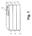
- Fig. 1 shows a flexible circuit board for three-dimensional shaping, comprising at least three layers 1, 2, 3, wherein a first layer 1 and a third layer 3 are made of metal and wherein the first layer 1 and the third layer 3, a second layer 2, which as Dielectric layer is designed to accommodate between them.
- the second layer 2 is formed as an adhesive, to which the first layer 1 and the third layer 3 are each bonded cohesively by lamination.
- Fig. 1 therefore also shows a flexible laminate for three-dimensional shaping, comprising at least three layers 1, 2, 3, wherein a first layer 1 and a third layer 3 are made of metal, wherein the first layer 1 and the third layer 3, a second layer 2, which is configured as a dielectric layer with a thermal conductivity, take up between them, and wherein the second layer 2 is formed as an adhesive to which the first layer 1 and the third layer 3 are each bonded cohesively.
- the laminate has a total thickness of between 45 and 440 ⁇ m, preferably between 100 ⁇ m and 250 ⁇ m.
- the second layer 2 is formed as an adhesive to which the first layer 1 and the third layer 3 are each connected only materially.
- the first layer 1 is made of aluminum and the third layer 3 is made of copper.
- the first layer 1 is 150 ⁇ m thick.
- the second layer 2 is 30 ⁇ m thick.
- the third layer 3 is 60 ⁇ m thick.
- the third layer 3 carries a conductive pattern 4.
- the conductive pattern 4 is produced by etching.
- This flexible printed circuit board has a total thickness between 45 and 440 microns, namely a total thickness of 240 microns.
- the adhesive has a thermal conductivity of 1 W / mK.
- Fig. 2 shows a flexible circuit board for three-dimensional shaping, comprising at least three layers 1 ', 2, 3, wherein a first layer 1' and a third layer 3 are made of metal and wherein the first layer 1 'and the third layer 3, a second layer. 2 , which is designed as a dielectric layer, take between them.
- the second layer 2 is formed as an adhesive, to which the first layer 1 'and the third layer 3 are each bonded cohesively by lamination.
- Fig. 2 also shows a flexible laminate for three-dimensional shaping, comprising at least three layers 1 ', 2, 3, wherein a first layer 1' and a third layer 3 are made of metal, wherein the first layer 1 'and the third layer 3, a second layer 2, which is designed as a dielectric layer with a thermal conductivity, take between them, and wherein the second layer 2 is formed as an adhesive to which the first layer 1 'and the third layer 3 are each connected materially.
- the laminate has a Total thickness between 45 and 440 microns, preferably between 100 microns and 250 microns, on.
- the second layer 2 is formed as an adhesive to which the first layer 1 'and the third layer 3 are each connected only materially.
- the first layer 1 ' is made of copper and the third layer 3 is also made of copper.
- the first layer 1 ' is 140 ⁇ m thick.
- the second layer 2 is 30 ⁇ m thick.
- the third layer 3 is 60 ⁇ m thick.
- the third layer 3 carries a conductive pattern 4.
- the conductive pattern 4 is produced by etching.
- This printed circuit board has a total thickness of between 45 and 440 ⁇ m, namely a total thickness of 230 ⁇ m.
- the adhesive has a thermal conductivity of 1 W / mK.
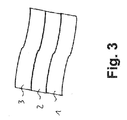
- Fig. 3 shows the circuit board according to Fig. 1 wherein the circuit board is deformed three-dimensionally.
Landscapes
- Engineering & Computer Science (AREA)
- Microelectronics & Electronic Packaging (AREA)
- Manufacturing & Machinery (AREA)
- Structure Of Printed Boards (AREA)
- Laminated Bodies (AREA)
Abstract
Ein flexibles Laminat zur dreidimensionalen Ausformung, umfassend mindestens drei Lagen (1, 1', 2, 3), wobei eine erste Lage (1, 1') und eine dritte Lage (3) aus Metall gefertigt sind, wobei die erste Lage (1, 1') und die dritte Lage (3) eine zweite Lage (2), welche als dielektrische Lage mit einer thermischen Leitfähigkeit ausgestaltet ist, zwischen sich aufnehmen, und wobei die zweite Lage (2) als Klebstoff ausgebildet ist, an welcher die erste Lage (1, 1') und die dritte Lage (3) jeweils stoffschlüssig angebunden sind, ist im Hinblick auf die Aufgabe, eine Leiterplatte derart auszugestalten und weiter zu bilden, dass diese bei möglichst guter thermischer Leitfähigkeit eine hohe Flexibilität zeigt, dadurch gekennzeichnet, dass das Laminat eine Gesamtdicke zwischen 45 und 440 µm, bevorzugt zwischen 100 µm und 250 µm, aufweist.
Description
- Die Erfindung betrifft ein Laminat nach dem Oberbegriff des Patentanspruchs 1.
- Aus der
JP 2007 110 010 A - Vor diesem Hintergrund sind bereits relativ starre IMS-Leiterplatten bekannt. IMS steht für "insulated metallic substrate". Unter IMS versteht der Fachmann ein Material für Leiterplatten, welches eine optimierte Wärmeableitung bewirkt, wie sie beispielsweise für Hochleistungselektroniken und Power LEDs erforderlich ist.
- Typischerweise wird auf eine Lage aus Aluminium, welche meist 1 mm dick oder dicker ist, ein gut wärmeleitendes Dielektrikum aufgetragen und dieses mit einer Lage aus Kupfer abgedeckt. Die Lage aus Kupfer wird dann zur Herstellung einer IMS-Leiterplatte strukturiert.
- Das verwendete Dielektrikum ist oft recht spröde und die Lagen aus Metall sind relativ dick. Daher können aus einem solchen Laminat (IMS) häufig nur sehr starre Leiterplatten hergestellt werden. Diese bekannten Leiterplatten sind aufgrund ihrer Starrheit nur wenig geeignet, dreidimensional geformt zu werden.
- Der Einsatz der bekannten IMS-Leiterplatten erfordert überdies aufwendige Verbindungstechnologien. Eine Verbindung kann beispielsweise über Kabel notwendig sein.
- Der Erfindung liegt daher die Aufgabe zugrunde, eine Leiterplatte der eingangs genannten Art derart auszugestalten und weiter zu bilden, dass diese bei möglichst guter thermischer Leitfähigkeit eine hohe Flexibilität zeigt.
- Die vorliegende Erfindung löst die zuvor genannte Aufgabe durch die Merkmale des Patentanspruchs 1.
- Erfindungsgemäß ist zunächst erkannt worden, dass ein Dielektrikum mit erhöhter thermischer Leitfähigkeit verwendet werden muss, um zwei sehr dünne, zunächst noch flexible Metalllagen zusammen zu laminieren, um daraus eine sehr flexible Leiterplatte zu fertigen. Weiter ist erkannt worden, dass die Verwendung eines geeigneten Dielektrikums für die Fertigung einer IMS ("insulated metallic substrate") - Leiterplatte notwendig ist. Das erfindungsgemäße Laminat zeigt eine sehr gute thermische Leitfähigkeit, wodurch dieses zur Entwärmung von Schaltungen und LEDs geeignet ist. Erfindungsgemäß ist insbesondere erkannt worden, dass das Laminat sehr dünn ausgestaltet sein muss, um die für eine dreidimensionale Ausgestaltung notwendige Flexibilität aufzuweisen. Das erfindungsgemäße Laminat ist derart flexibel, dass eine mit diesem gefertigte Leiterplatte als dreidimensionale Struktur verbaut werden kann. Trotz einer sehr hohen thermischen Leitfähigkeit der dielektrischen Lage bleiben die Materialien, aus der die Leiterplatte besteht, ausreichend flexibel. So ist eine Leiterplatte, die das erfindungsgemäße Laminat aufweist, als vorgefertigte Schaltung dreidimensional ausgeformt in einer dreidimensional gestalteten Struktur, insbesondere einem Scheinwerfer, verbaubar. Insoweit ist eine Leiterplatte realisierbar, welche bei möglichst guter thermischer Leitfähigkeit eine hohe Flexibilität zeigt.
- Folglich ist die eingangs genannte Aufgabe gelöst.
- Die zweite Lage könnte als Klebstoff ausgebildet sein, an welcher die erste Lage und die dritte Lage jeweils ausschließlich stoffschlüssig angebunden sind. So kann auf mechanische Anbindemittel verzichtet werden. Die Anbindung kann durch Laminieren erfolgen.
- Die erste Lage könnte aus Aluminium und die dritte Lage könnte aus Kupfer gefertigt sein. Aluminium ist ein relativ leichter Werkstoff. In Kupfer können sehr gut leitende Leitungen oder Leitungsbilder eingebracht werden.
- Die erste Lage könnte aus Kupfer und die dritte Lage könnte ebenfalls aus Kupfer gefertigt sein. Hierdurch ist eine Materialeinheitlichkeit gegeben, die die Lagerhaltung und Logistik vereinfacht.
- Die erste Lage könnte zwischen 25 und 300 µm dick sein. Durch Wahl dieses Dickenbereichs bleibt die Flexibilität des IMS-Materials und damit die Flexibilität der daraus hergestellten Leiterplatte erhalten.
- Die zweite Lage könnte zwischen 10 und 70 µm dick sein. Die mechanischen Eigenschaften einer flexiblen Leiterplatte werden mit dem Vorteil einer erhöhten thermischen Leitfähigkeit einer IMS-Schaltung kombiniert.
- Vor diesem Hintergrund könnte die dritte Lage könnte zwischen 10 und 70 µm dick sein. Durch Wahl dieses Dickenbereichs bleibt die Flexibilität des IMS-Materials und damit die Flexibilität der daraus hergestellten Leiterplatte erhalten.
- Der Klebstoff könnte eine thermische Leitfähigkeit zwischen 0,25 und 3,5 W/mK aufweisen. Eine ein solches Laminat umfassende Leiterplatte kann zur Entwärmung von Hochleistungselektroniken oder von Power-LED-Schaltungen in Scheinwerfern verwendet werden. Die thermische Leitfähigkeit wird nach DIN EN ISO 22007-04:2012 mittels eines Flash-Verfahrens bestimmt.
- Die dritte Lage könnte ein Leiterbild tragen. Hierdurch ist eine Leiterplatte als IMS-Leiterplatte ausgestaltet und kann in Scheinwerfern von Fahrzeugen verwendet werden.
- Das Leiterbild könnte ätztechnisch hergestellt sein. Durch ein Ätzverfahren können sehr exakte Leiterbilder geschaffen werden.
- Konkret kann eine hier beschriebene Leiterplatte im Außenlichtbereich von Fahrzeugen verwendet werden, da sie eine Entwärmung einer Power-LED-Schaltung bewirken kann. Im Außenlichtbereich ist oft eine dreidimensionale Anordnung einer LED gefordert.
- In der Zeichnung zeigen
- Fig. 1
- eine ebene Leiterplatte, die aus drei Lagen aufgebaut ist, wobei die drei Lagen ein Laminat bilden,
- Fig. 2
- eine weitere ebene Leiterplatte, die aus drei Lagen aufgebaut ist, und
- Fig. 3
- die Leiterplatte gemäß
Fig. 1 , wobei die Leiterplatte dreidimensional verformt ist. -
Fig. 1 zeigt eine flexible Leiterplatte zur dreidimensionalen Ausformung, umfassend mindestens drei Lagen 1, 2, 3, wobei eine erste Lage 1 und eine dritte Lage 3 aus Metall gefertigt sind und wobei die erste Lage 1 und die dritte Lage 3 eine zweite Lage 2, welche als dielektrische Lage ausgestaltet ist, zwischen sich aufnehmen. Die zweite Lage 2 ist als Klebstoff ausgebildet, an welcher die erste Lage 1 und die dritte Lage 3 jeweils stoffschlüssig durch Laminieren angebunden sind. -
Fig. 1 zeigt daher auch ein flexibles Laminat zur dreidimensionalen Ausformung, umfassend mindestens drei Lagen 1, 2, 3, wobei eine erste Lage 1 und eine dritte Lage 3 aus Metall gefertigt sind, wobei die erste Lage 1 und die dritte Lage 3 eine zweite Lage 2, welche als dielektrische Lage mit einer thermischen Leitfähigkeit ausgestaltet ist, zwischen sich aufnehmen, und wobei die zweite Lage 2 als Klebstoff ausgebildet ist, an welcher die erste Lage 1 und die dritte Lage 3 jeweils stoffschlüssig angebunden sind. Das Laminat weist eine Gesamtdicke zwischen 45 und 440 µm, bevorzugt zwischen 100 µm und 250 µm, auf. - Die zweite Lage 2 ist als Klebstoff ausgebildet, an welcher die erste Lage 1 und die dritte Lage 3 jeweils ausschließlich stoffschlüssig angebunden sind.
- Die erste Lage 1 ist aus Aluminium und die dritte Lage 3 ist aus Kupfer gefertigt.
- Die erste Lage 1 ist 150 µm dick. Die zweite Lage 2 ist 30 µm dick. Die dritte Lage 3 ist 60 µm dick. Die dritte Lage 3 trägt ein Leiterbild 4. Das Leiterbild 4 ist ätztechnisch hergestellt.
- Diese flexible Leiterplatte weist eine Gesamtdicke zwischen 45 und 440 µm, nämlich eine Gesamtdicke von 240 µm auf.
- Der Klebstoff weist eine thermische Leitfähigkeit von 1 W/mK auf.
-
Fig. 2 zeigt eine flexible Leiterplatte zur dreidimensionalen Ausformung, umfassend mindestens drei Lagen 1', 2, 3, wobei eine erste Lage 1' und eine dritte Lage 3 aus Metall gefertigt sind und wobei die erste Lage 1' und die dritte Lage 3 eine zweite Lage 2, welche als dielektrische Lage ausgestaltet ist, zwischen sich aufnehmen. Die zweite Lage 2 ist als Klebstoff ausgebildet, an welcher die erste Lage 1' und die dritte Lage 3 jeweils stoffschlüssig durch Laminieren angebunden sind. -
Fig. 2 zeigt auch ein flexibles Laminat zur dreidimensionalen Ausformung, umfassend mindestens drei Lagen 1', 2, 3, wobei eine erste Lage 1' und eine dritte Lage 3 aus Metall gefertigt sind, wobei die erste Lage 1' und die dritte Lage 3 eine zweite Lage 2, welche als dielektrische Lage mit einer thermischen Leitfähigkeit ausgestaltet ist, zwischen sich aufnehmen, und wobei die zweite Lage 2 als Klebstoff ausgebildet ist, an welcher die erste Lage 1' und die dritte Lage 3 jeweils stoffschlüssig angebunden sind. Das Laminat weist eine Gesamtdicke zwischen 45 und 440 µm, bevorzugt zwischen 100 µm und 250 µm, auf. - Die zweite Lage 2 ist als Klebstoff ausgebildet, an welcher die erste Lage 1' und die dritte Lage 3 jeweils ausschließlich stoffschlüssig angebunden sind.
- Die erste Lage 1' ist aus Kupfer und die dritte Lage 3 ist auch aus Kupfer gefertigt. Die erste Lage 1' ist 140 µm dick. Die zweite Lage 2 ist 30 µm dick. Die dritte Lage 3 ist 60 µm dick. Die dritte Lage 3 trägt ein Leiterbild 4. Das Leiterbild 4 ist ätztechnisch hergestellt.
- Diese Leiterplatte weist eine Gesamtdicke zwischen 45 und 440 µm, nämlich eine Gesamtdicke von 230 µm, auf.
- Der Klebstoff weist eine thermische Leitfähigkeit von 1 W/mK auf.
-
Fig. 3 zeigt die Leiterplatte gemäßFig. 1 , wobei die Leiterplatte dreidimensional verformt ist.
Claims (10)
- Flexibles Laminat zur dreidimensionalen Ausformung, umfassend mindestens drei Lagen (1, 1', 2, 3), wobei eine erste Lage (1, 1') und eine dritte Lage (3) aus Metall gefertigt sind, wobei die erste Lage (1, 1') und die dritte Lage (3) eine zweite Lage (2), welche als dielektrische Lage mit einer thermischen Leitfähigkeit ausgestaltet ist, zwischen sich aufnehmen, und wobei die zweite Lage (2) als Klebstoff ausgebildet ist, an welcher die erste Lage (1, 1') und die dritte Lage (3) jeweils stoffschlüssig angebunden sind,
dadurch gekennzeichnet, dass das Laminat eine Gesamtdicke zwischen 45 und 440 µm, bevorzugt zwischen 100 µm und 250 µm, aufweist. - Laminat nach Anspruch 1, dadurch gekennzeichnet, dass die zweite Lage (2) als Klebstoff ausgebildet ist, an welcher die erste Lage (1, 1') und die dritte Lage (3) jeweils ausschließlich stoffschlüssig angebunden sind.
- Laminat nach Anspruch 1 oder 2, dadurch gekennzeichnet, dass die erste Lage (1) aus Aluminium und die dritte Lage (3) aus Kupfer gefertigt ist.
- Laminat nach Anspruch 1 oder 2, dadurch gekennzeichnet, dass die erste Lage (1') aus Kupfer und die dritte Lage (3) aus Kupfer gefertigt ist.
- Laminat nach einem der voranstehenden Ansprüche, dadurch gekennzeichnet, dass die erste Lage (1, 1') zwischen 25 und 300 µm dick ist.
- Laminat nach einem der voranstehenden Ansprüche, dadurch gekennzeichnet, dass die zweite Lage (2) zwischen 10 und 70 µm dick ist.
- Laminat nach einem der voranstehenden Ansprüche, dadurch gekennzeichnet, dass die dritte Lage (3) zwischen 10 und 70 µm dick ist.
- Laminat nach einem der voranstehenden Ansprüche, dadurch gekennzeichnet, dass der Klebstoff eine thermische Leitfähigkeit zwischen 0,25 und 3,5 W/mK aufweist.
- Flexible Leiterplatte, umfassend ein Laminat nach einem der voranstehenden Ansprüche, dadurch gekennzeichnet, dass die dritte Lage (3) ein Leiterbild (4) trägt.
- Leiterplatte nach Anspruch 9, dadurch gekennzeichnet, dass das Leiterbild (4) ätztechnisch hergestellt ist.
Applications Claiming Priority (1)
| Application Number | Priority Date | Filing Date | Title |
|---|---|---|---|
| DE102014010329.3A DE102014010329A1 (de) | 2014-07-14 | 2014-07-14 | Laminat zur Herstellung einer IMS-Leiterplatte und IMS-Leiterplatte |
Publications (1)
| Publication Number | Publication Date |
|---|---|
| EP2975916A1 true EP2975916A1 (de) | 2016-01-20 |
Family
ID=53489840
Family Applications (1)
| Application Number | Title | Priority Date | Filing Date |
|---|---|---|---|
| EP15172854.0A Withdrawn EP2975916A1 (de) | 2014-07-14 | 2015-06-19 | Laminat zur herstellung einer ims-leiterplatte und ims-leiterplatte |
Country Status (2)
| Country | Link |
|---|---|
| EP (1) | EP2975916A1 (de) |
| DE (1) | DE102014010329A1 (de) |
Citations (4)
| Publication number | Priority date | Publication date | Assignee | Title |
|---|---|---|---|---|
| DE10151640A1 (de) * | 2001-10-11 | 2003-05-08 | Krempel August Soehne | Basislaminat für flexible gedruckte Schaltungen und Deckfolie hierfür |
| JP2007110010A (ja) | 2005-10-17 | 2007-04-26 | Shindo Denshi Kogyo Kk | フレキシブルプリント配線板、フレキシブルプリント回路板、およびそれらの製造方法 |
| EP1874101A1 (de) * | 2005-04-19 | 2008-01-02 | Denki Kagaku Kogyo Kabushiki Kaisha | Leiterplatte mit metallbasis, led und led-lichtquelleneinheit |
| WO2009073670A1 (en) * | 2007-12-04 | 2009-06-11 | E. I. Du Pont De Nemours And Company | Bendable circuit structure for led mounting and interconnection |
-
2014
- 2014-07-14 DE DE102014010329.3A patent/DE102014010329A1/de not_active Ceased
-
2015
- 2015-06-19 EP EP15172854.0A patent/EP2975916A1/de not_active Withdrawn
Patent Citations (4)
| Publication number | Priority date | Publication date | Assignee | Title |
|---|---|---|---|---|
| DE10151640A1 (de) * | 2001-10-11 | 2003-05-08 | Krempel August Soehne | Basislaminat für flexible gedruckte Schaltungen und Deckfolie hierfür |
| EP1874101A1 (de) * | 2005-04-19 | 2008-01-02 | Denki Kagaku Kogyo Kabushiki Kaisha | Leiterplatte mit metallbasis, led und led-lichtquelleneinheit |
| JP2007110010A (ja) | 2005-10-17 | 2007-04-26 | Shindo Denshi Kogyo Kk | フレキシブルプリント配線板、フレキシブルプリント回路板、およびそれらの製造方法 |
| WO2009073670A1 (en) * | 2007-12-04 | 2009-06-11 | E. I. Du Pont De Nemours And Company | Bendable circuit structure for led mounting and interconnection |
Also Published As
| Publication number | Publication date |
|---|---|
| DE102014010329A1 (de) | 2016-01-14 |
Similar Documents
| Publication | Publication Date | Title |
|---|---|---|
| AT515101B1 (de) | Verfahren zum Einbetten einer Komponente in eine Leiterplatte | |
| DE102008054288A1 (de) | Verfahren zum Herstellen eines flexiblen Leuchtbands | |
| DE102011088970A1 (de) | Steuergerät und Verfahren zum Herstellen eines Steuergeräts für ein Kraftfahrzeug | |
| EP0620702B1 (de) | Kern für elektrische Verbindungssubstrate und elektrische Verbindungssubstrate mit Kern, sowie Verfahren zu deren Herstellung | |
| DE112017004465T5 (de) | Flexible gedruckte Leiterplatte und Verfahren zum Herstellen einer flexiblen gedruckten Leiterplatte | |
| EP1550358B1 (de) | Leiterplatte mit mindestens einem starren und mindestens einem flexiblen bereich sowie verfahren zur herstellung von starr-flexiblen leiterplatten | |
| DE102011080153A1 (de) | Flexible verbindung von substraten in leistungshalbleitermodulen | |
| DE102014218821A1 (de) | Leiterplatte | |
| DE102005011857B4 (de) | Flächige Beleuchtungseinrichtung | |
| DE102005056014A1 (de) | Elektroniksteuermodul mit einer inneren elektrischen Erdung und Verfahren zu seiner Herstellung | |
| DE102013016073B4 (de) | Vorrichtung zur Signalübertragung in einem Fahrzeug | |
| DE10108168C1 (de) | Verfahren zur Herstellung einer Multiwire-Leiterplatte | |
| DE102021004458A1 (de) | Leiterplatte und Schaltungsanordnung | |
| DE102011084303A1 (de) | Verfahren zur Herstellung eines Trägers für eine leistungselektronische Baugruppe und Träger für eine solche Baugruppe | |
| DE102014010329A1 (de) | Laminat zur Herstellung einer IMS-Leiterplatte und IMS-Leiterplatte | |
| WO2010043540A1 (de) | Verfahren zur herstellung eines mit elektrischen elementen versehenen duktilen substrats | |
| DE102019116021B4 (de) | Flexible Leiterplatte mit thermisch leitender Verbindung zu einer Wärmesenke | |
| DE102020100742B4 (de) | Lichtmodul, Beleuchtungseinrichtung und Kraftfahrzeug | |
| EP1592288A1 (de) | Leiterplatte | |
| DE102009035850A1 (de) | Leiterplattenordnung mit Keramikplatte und Grafitschicht | |
| EP3066898B1 (de) | Leiterplattenstruktur | |
| WO2018202245A1 (de) | Kühlkörper | |
| DE202013008406U1 (de) | Leiterplattenstromschiene | |
| DE4427112A1 (de) | Leiterplattenanordnung | |
| DE102012207107A1 (de) | Mehrschichtplatine |
Legal Events
| Date | Code | Title | Description |
|---|---|---|---|
| PUAI | Public reference made under article 153(3) epc to a published international application that has entered the european phase |
Free format text: ORIGINAL CODE: 0009012 |
|
| AK | Designated contracting states |
Kind code of ref document: A1 Designated state(s): AL AT BE BG CH CY CZ DE DK EE ES FI FR GB GR HR HU IE IS IT LI LT LU LV MC MK MT NL NO PL PT RO RS SE SI SK SM TR |
|
| AX | Request for extension of the european patent |
Extension state: BA ME |
|
| RAP1 | Party data changed (applicant data changed or rights of an application transferred) |
Owner name: MEKTEC EUROPE GMBH |
|
| STAA | Information on the status of an ep patent application or granted ep patent |
Free format text: STATUS: THE APPLICATION IS DEEMED TO BE WITHDRAWN |
|
| 18D | Application deemed to be withdrawn |
Effective date: 20160721 |