EP2974859A1 - Bonded body, substrate for power modules, and substrate with heat sink for power modules - Google Patents
Bonded body, substrate for power modules, and substrate with heat sink for power modules Download PDFInfo
- Publication number
- EP2974859A1 EP2974859A1 EP14765031.1A EP14765031A EP2974859A1 EP 2974859 A1 EP2974859 A1 EP 2974859A1 EP 14765031 A EP14765031 A EP 14765031A EP 2974859 A1 EP2974859 A1 EP 2974859A1
- Authority
- EP
- European Patent Office
- Prior art keywords
- layer
- bonding
- aluminum
- metal
- power module
- Prior art date
- Legal status (The legal status is an assumption and is not a legal conclusion. Google has not performed a legal analysis and makes no representation as to the accuracy of the status listed.)
- Granted
Links
- 239000000758 substrate Substances 0.000 title claims description 170
- 229910052751 metal Inorganic materials 0.000 claims abstract description 243
- 239000002184 metal Substances 0.000 claims abstract description 243
- 229910004339 Ti-Si Inorganic materials 0.000 claims abstract description 195
- 229910010978 Ti—Si Inorganic materials 0.000 claims abstract description 195
- 229910052782 aluminium Inorganic materials 0.000 claims abstract description 192
- XAGFODPZIPBFFR-UHFFFAOYSA-N aluminium Chemical compound [Al] XAGFODPZIPBFFR-UHFFFAOYSA-N 0.000 claims abstract description 192
- 239000010949 copper Substances 0.000 claims abstract description 164
- 239000010936 titanium Substances 0.000 claims abstract description 149
- 229910052802 copper Inorganic materials 0.000 claims abstract description 113
- RYGMFSIKBFXOCR-UHFFFAOYSA-N Copper Chemical compound [Cu] RYGMFSIKBFXOCR-UHFFFAOYSA-N 0.000 claims abstract description 112
- PXHVJJICTQNCMI-UHFFFAOYSA-N Nickel Chemical compound [Ni] PXHVJJICTQNCMI-UHFFFAOYSA-N 0.000 claims abstract description 74
- 229910052709 silver Inorganic materials 0.000 claims abstract description 27
- BQCADISMDOOEFD-UHFFFAOYSA-N Silver Chemical compound [Ag] BQCADISMDOOEFD-UHFFFAOYSA-N 0.000 claims abstract description 26
- 239000004332 silver Substances 0.000 claims abstract description 26
- 229910052759 nickel Inorganic materials 0.000 claims abstract description 24
- 229910000679 solder Inorganic materials 0.000 claims description 47
- 238000009413 insulation Methods 0.000 claims description 35
- 239000000919 ceramic Substances 0.000 description 83
- 238000009792 diffusion process Methods 0.000 description 66
- RTAQQCXQSZGOHL-UHFFFAOYSA-N Titanium Chemical compound [Ti] RTAQQCXQSZGOHL-UHFFFAOYSA-N 0.000 description 51
- 239000007790 solid phase Substances 0.000 description 51
- 239000004065 semiconductor Substances 0.000 description 46
- NDVLTYZPCACLMA-UHFFFAOYSA-N silver oxide Chemical compound [O-2].[Ag+].[Ag+] NDVLTYZPCACLMA-UHFFFAOYSA-N 0.000 description 32
- 239000000463 material Substances 0.000 description 26
- 238000012360 testing method Methods 0.000 description 26
- 238000010438 heat treatment Methods 0.000 description 22
- 238000004519 manufacturing process Methods 0.000 description 18
- 229910018575 Al—Ti Inorganic materials 0.000 description 16
- 229910001923 silver oxide Inorganic materials 0.000 description 16
- 239000011888 foil Substances 0.000 description 15
- 229910000881 Cu alloy Inorganic materials 0.000 description 14
- 238000003475 lamination Methods 0.000 description 14
- 230000000052 comparative effect Effects 0.000 description 13
- 229910000838 Al alloy Inorganic materials 0.000 description 12
- 229910004353 Ti-Cu Inorganic materials 0.000 description 12
- PMHQVHHXPFUNSP-UHFFFAOYSA-M copper(1+);methylsulfanylmethane;bromide Chemical compound Br[Cu].CSC PMHQVHHXPFUNSP-UHFFFAOYSA-M 0.000 description 12
- VZSRBBMJRBPUNF-UHFFFAOYSA-N 2-(2,3-dihydro-1H-inden-2-ylamino)-N-[3-oxo-3-(2,4,6,7-tetrahydrotriazolo[4,5-c]pyridin-5-yl)propyl]pyrimidine-5-carboxamide Chemical compound C1C(CC2=CC=CC=C12)NC1=NC=C(C=N1)C(=O)NCCC(N1CC2=C(CC1)NN=N2)=O VZSRBBMJRBPUNF-UHFFFAOYSA-N 0.000 description 11
- 238000005219 brazing Methods 0.000 description 11
- 238000010586 diagram Methods 0.000 description 11
- 239000000945 filler Substances 0.000 description 11
- 229910018125 Al-Si Inorganic materials 0.000 description 10
- 229910018520 Al—Si Inorganic materials 0.000 description 10
- 238000007747 plating Methods 0.000 description 10
- 238000000034 method Methods 0.000 description 9
- 238000010030 laminating Methods 0.000 description 8
- 230000015572 biosynthetic process Effects 0.000 description 7
- 230000000694 effects Effects 0.000 description 6
- 230000014759 maintenance of location Effects 0.000 description 6
- HMUNWXXNJPVALC-UHFFFAOYSA-N 1-[4-[2-(2,3-dihydro-1H-inden-2-ylamino)pyrimidin-5-yl]piperazin-1-yl]-2-(2,4,6,7-tetrahydrotriazolo[4,5-c]pyridin-5-yl)ethanone Chemical compound C1C(CC2=CC=CC=C12)NC1=NC=C(C=N1)N1CCN(CC1)C(CN1CC2=C(CC1)NN=N2)=O HMUNWXXNJPVALC-UHFFFAOYSA-N 0.000 description 5
- 229910001316 Ag alloy Inorganic materials 0.000 description 5
- 229910000990 Ni alloy Inorganic materials 0.000 description 5
- 229910052581 Si3N4 Inorganic materials 0.000 description 5
- PNEYBMLMFCGWSK-UHFFFAOYSA-N aluminium oxide Inorganic materials [O-2].[O-2].[O-2].[Al+3].[Al+3] PNEYBMLMFCGWSK-UHFFFAOYSA-N 0.000 description 5
- 238000011156 evaluation Methods 0.000 description 5
- 239000007791 liquid phase Substances 0.000 description 5
- 239000000126 substance Substances 0.000 description 5
- NPXOKRUENSOPAO-UHFFFAOYSA-N Raney nickel Chemical compound [Al].[Ni] NPXOKRUENSOPAO-UHFFFAOYSA-N 0.000 description 4
- 229910020935 Sn-Sb Inorganic materials 0.000 description 4
- 229910008757 Sn—Sb Inorganic materials 0.000 description 4
- -1 aluminum Silver Chemical compound 0.000 description 4
- 239000003638 chemical reducing agent Substances 0.000 description 4
- 230000000873 masking effect Effects 0.000 description 4
- 239000002245 particle Substances 0.000 description 4
- 230000008646 thermal stress Effects 0.000 description 4
- 229910017944 Ag—Cu Inorganic materials 0.000 description 3
- 229910020836 Sn-Ag Inorganic materials 0.000 description 3
- 229910020888 Sn-Cu Inorganic materials 0.000 description 3
- 229910020988 Sn—Ag Inorganic materials 0.000 description 3
- 229910019204 Sn—Cu Inorganic materials 0.000 description 3
- 229910018956 Sn—In Inorganic materials 0.000 description 3
- 230000003647 oxidation Effects 0.000 description 3
- 238000007254 oxidation reaction Methods 0.000 description 3
- 239000012071 phase Substances 0.000 description 3
- 238000005476 soldering Methods 0.000 description 3
- 239000011248 coating agent Substances 0.000 description 2
- 238000000576 coating method Methods 0.000 description 2
- 238000012790 confirmation Methods 0.000 description 2
- 238000001816 cooling Methods 0.000 description 2
- 229910052593 corundum Inorganic materials 0.000 description 2
- 230000003247 decreasing effect Effects 0.000 description 2
- 238000001514 detection method Methods 0.000 description 2
- 238000007772 electroless plating Methods 0.000 description 2
- 238000004453 electron probe microanalysis Methods 0.000 description 2
- 238000002474 experimental method Methods 0.000 description 2
- 239000012530 fluid Substances 0.000 description 2
- 230000017525 heat dissipation Effects 0.000 description 2
- 230000008642 heat stress Effects 0.000 description 2
- 239000012535 impurity Substances 0.000 description 2
- 238000005259 measurement Methods 0.000 description 2
- 238000002844 melting Methods 0.000 description 2
- 230000008018 melting Effects 0.000 description 2
- 239000000523 sample Substances 0.000 description 2
- 238000001878 scanning electron micrograph Methods 0.000 description 2
- HQVNEWCFYHHQES-UHFFFAOYSA-N silicon nitride Chemical compound N12[Si]34N5[Si]62N3[Si]51N64 HQVNEWCFYHHQES-UHFFFAOYSA-N 0.000 description 2
- 238000012546 transfer Methods 0.000 description 2
- 229910001845 yogo sapphire Inorganic materials 0.000 description 2
- LDXJRKWFNNFDSA-UHFFFAOYSA-N 2-(2,4,6,7-tetrahydrotriazolo[4,5-c]pyridin-5-yl)-1-[4-[2-[[3-(trifluoromethoxy)phenyl]methylamino]pyrimidin-5-yl]piperazin-1-yl]ethanone Chemical compound C1CN(CC2=NNN=C21)CC(=O)N3CCN(CC3)C4=CN=C(N=C4)NCC5=CC(=CC=C5)OC(F)(F)F LDXJRKWFNNFDSA-UHFFFAOYSA-N 0.000 description 1
- YLZOPXRUQYQQID-UHFFFAOYSA-N 3-(2,4,6,7-tetrahydrotriazolo[4,5-c]pyridin-5-yl)-1-[4-[2-[[3-(trifluoromethoxy)phenyl]methylamino]pyrimidin-5-yl]piperazin-1-yl]propan-1-one Chemical compound N1N=NC=2CN(CCC=21)CCC(=O)N1CCN(CC1)C=1C=NC(=NC=1)NCC1=CC(=CC=C1)OC(F)(F)F YLZOPXRUQYQQID-UHFFFAOYSA-N 0.000 description 1
- DEXFNLNNUZKHNO-UHFFFAOYSA-N 6-[3-[4-[2-(2,3-dihydro-1H-inden-2-ylamino)pyrimidin-5-yl]piperidin-1-yl]-3-oxopropyl]-3H-1,3-benzoxazol-2-one Chemical compound C1C(CC2=CC=CC=C12)NC1=NC=C(C=N1)C1CCN(CC1)C(CCC1=CC2=C(NC(O2)=O)C=C1)=O DEXFNLNNUZKHNO-UHFFFAOYSA-N 0.000 description 1
- MKYBYDHXWVHEJW-UHFFFAOYSA-N N-[1-oxo-1-(2,4,6,7-tetrahydrotriazolo[4,5-c]pyridin-5-yl)propan-2-yl]-2-[[3-(trifluoromethoxy)phenyl]methylamino]pyrimidine-5-carboxamide Chemical compound O=C(C(C)NC(=O)C=1C=NC(=NC=1)NCC1=CC(=CC=C1)OC(F)(F)F)N1CC2=C(CC1)NN=N2 MKYBYDHXWVHEJW-UHFFFAOYSA-N 0.000 description 1
- NIPNSKYNPDTRPC-UHFFFAOYSA-N N-[2-oxo-2-(2,4,6,7-tetrahydrotriazolo[4,5-c]pyridin-5-yl)ethyl]-2-[[3-(trifluoromethoxy)phenyl]methylamino]pyrimidine-5-carboxamide Chemical compound O=C(CNC(=O)C=1C=NC(=NC=1)NCC1=CC(=CC=C1)OC(F)(F)F)N1CC2=C(CC1)NN=N2 NIPNSKYNPDTRPC-UHFFFAOYSA-N 0.000 description 1
- AFCARXCZXQIEQB-UHFFFAOYSA-N N-[3-oxo-3-(2,4,6,7-tetrahydrotriazolo[4,5-c]pyridin-5-yl)propyl]-2-[[3-(trifluoromethoxy)phenyl]methylamino]pyrimidine-5-carboxamide Chemical compound O=C(CCNC(=O)C=1C=NC(=NC=1)NCC1=CC(=CC=C1)OC(F)(F)F)N1CC2=C(CC1)NN=N2 AFCARXCZXQIEQB-UHFFFAOYSA-N 0.000 description 1
- 229910004337 Ti-Ni Inorganic materials 0.000 description 1
- 229910011209 Ti—Ni Inorganic materials 0.000 description 1
- 238000004458 analytical method Methods 0.000 description 1
- 239000004020 conductor Substances 0.000 description 1
- 230000007797 corrosion Effects 0.000 description 1
- 238000005260 corrosion Methods 0.000 description 1
- 230000006866 deterioration Effects 0.000 description 1
- 150000002500 ions Chemical class 0.000 description 1
- 239000000203 mixture Substances 0.000 description 1
- 238000012545 processing Methods 0.000 description 1
- 239000010944 silver (metal) Substances 0.000 description 1
- 238000000992 sputter etching Methods 0.000 description 1
- 229910052719 titanium Inorganic materials 0.000 description 1
- 230000001052 transient effect Effects 0.000 description 1
Images


Classifications
-
- H—ELECTRICITY
- H05—ELECTRIC TECHNIQUES NOT OTHERWISE PROVIDED FOR
- H05K—PRINTED CIRCUITS; CASINGS OR CONSTRUCTIONAL DETAILS OF ELECTRIC APPARATUS; MANUFACTURE OF ASSEMBLAGES OF ELECTRICAL COMPONENTS
- H05K1/00—Printed circuits
- H05K1/02—Details
- H05K1/09—Use of materials for the conductive, e.g. metallic pattern
-
- C—CHEMISTRY; METALLURGY
- C04—CEMENTS; CONCRETE; ARTIFICIAL STONE; CERAMICS; REFRACTORIES
- C04B—LIME, MAGNESIA; SLAG; CEMENTS; COMPOSITIONS THEREOF, e.g. MORTARS, CONCRETE OR LIKE BUILDING MATERIALS; ARTIFICIAL STONE; CERAMICS; REFRACTORIES; TREATMENT OF NATURAL STONE
- C04B37/00—Joining burned ceramic articles with other burned ceramic articles or other articles by heating
- C04B37/02—Joining burned ceramic articles with other burned ceramic articles or other articles by heating with metallic articles
- C04B37/023—Joining burned ceramic articles with other burned ceramic articles or other articles by heating with metallic articles characterised by the interlayer used
- C04B37/026—Joining burned ceramic articles with other burned ceramic articles or other articles by heating with metallic articles characterised by the interlayer used consisting of metals or metal salts
-
- B—PERFORMING OPERATIONS; TRANSPORTING
- B23—MACHINE TOOLS; METAL-WORKING NOT OTHERWISE PROVIDED FOR
- B23K—SOLDERING OR UNSOLDERING; WELDING; CLADDING OR PLATING BY SOLDERING OR WELDING; CUTTING BY APPLYING HEAT LOCALLY, e.g. FLAME CUTTING; WORKING BY LASER BEAM
- B23K20/00—Non-electric welding by applying impact or other pressure, with or without the application of heat, e.g. cladding or plating
- B23K20/02—Non-electric welding by applying impact or other pressure, with or without the application of heat, e.g. cladding or plating by means of a press ; Diffusion bonding
- B23K20/023—Thermo-compression bonding
- B23K20/026—Thermo-compression bonding with diffusion of soldering material
-
- B—PERFORMING OPERATIONS; TRANSPORTING
- B23—MACHINE TOOLS; METAL-WORKING NOT OTHERWISE PROVIDED FOR
- B23K—SOLDERING OR UNSOLDERING; WELDING; CLADDING OR PLATING BY SOLDERING OR WELDING; CUTTING BY APPLYING HEAT LOCALLY, e.g. FLAME CUTTING; WORKING BY LASER BEAM
- B23K20/00—Non-electric welding by applying impact or other pressure, with or without the application of heat, e.g. cladding or plating
- B23K20/16—Non-electric welding by applying impact or other pressure, with or without the application of heat, e.g. cladding or plating with interposition of special material to facilitate connection of the parts, e.g. material for absorbing or producing gas
-
- B—PERFORMING OPERATIONS; TRANSPORTING
- B23—MACHINE TOOLS; METAL-WORKING NOT OTHERWISE PROVIDED FOR
- B23K—SOLDERING OR UNSOLDERING; WELDING; CLADDING OR PLATING BY SOLDERING OR WELDING; CUTTING BY APPLYING HEAT LOCALLY, e.g. FLAME CUTTING; WORKING BY LASER BEAM
- B23K20/00—Non-electric welding by applying impact or other pressure, with or without the application of heat, e.g. cladding or plating
- B23K20/22—Non-electric welding by applying impact or other pressure, with or without the application of heat, e.g. cladding or plating taking account of the properties of the materials to be welded
- B23K20/233—Non-electric welding by applying impact or other pressure, with or without the application of heat, e.g. cladding or plating taking account of the properties of the materials to be welded without ferrous layer
-
- B—PERFORMING OPERATIONS; TRANSPORTING
- B23—MACHINE TOOLS; METAL-WORKING NOT OTHERWISE PROVIDED FOR
- B23K—SOLDERING OR UNSOLDERING; WELDING; CLADDING OR PLATING BY SOLDERING OR WELDING; CUTTING BY APPLYING HEAT LOCALLY, e.g. FLAME CUTTING; WORKING BY LASER BEAM
- B23K35/00—Rods, electrodes, materials, or media, for use in soldering, welding, or cutting
- B23K35/001—Interlayers, transition pieces for metallurgical bonding of workpieces
- B23K35/002—Interlayers, transition pieces for metallurgical bonding of workpieces at least one of the workpieces being of light metal
-
- B—PERFORMING OPERATIONS; TRANSPORTING
- B23—MACHINE TOOLS; METAL-WORKING NOT OTHERWISE PROVIDED FOR
- B23K—SOLDERING OR UNSOLDERING; WELDING; CLADDING OR PLATING BY SOLDERING OR WELDING; CUTTING BY APPLYING HEAT LOCALLY, e.g. FLAME CUTTING; WORKING BY LASER BEAM
- B23K35/00—Rods, electrodes, materials, or media, for use in soldering, welding, or cutting
- B23K35/001—Interlayers, transition pieces for metallurgical bonding of workpieces
- B23K35/005—Interlayers, transition pieces for metallurgical bonding of workpieces at least one of the workpieces being of a refractory metal
-
- B—PERFORMING OPERATIONS; TRANSPORTING
- B32—LAYERED PRODUCTS
- B32B—LAYERED PRODUCTS, i.e. PRODUCTS BUILT-UP OF STRATA OF FLAT OR NON-FLAT, e.g. CELLULAR OR HONEYCOMB, FORM
- B32B15/00—Layered products comprising a layer of metal
- B32B15/01—Layered products comprising a layer of metal all layers being exclusively metallic
- B32B15/017—Layered products comprising a layer of metal all layers being exclusively metallic one layer being formed of aluminium or an aluminium alloy, another layer being formed of an alloy based on a non ferrous metal other than aluminium
-
- C—CHEMISTRY; METALLURGY
- C22—METALLURGY; FERROUS OR NON-FERROUS ALLOYS; TREATMENT OF ALLOYS OR NON-FERROUS METALS
- C22C—ALLOYS
- C22C13/00—Alloys based on tin
-
- C—CHEMISTRY; METALLURGY
- C22—METALLURGY; FERROUS OR NON-FERROUS ALLOYS; TREATMENT OF ALLOYS OR NON-FERROUS METALS
- C22C—ALLOYS
- C22C13/00—Alloys based on tin
- C22C13/02—Alloys based on tin with antimony or bismuth as the next major constituent
-
- C—CHEMISTRY; METALLURGY
- C22—METALLURGY; FERROUS OR NON-FERROUS ALLOYS; TREATMENT OF ALLOYS OR NON-FERROUS METALS
- C22C—ALLOYS
- C22C21/00—Alloys based on aluminium
-
- C—CHEMISTRY; METALLURGY
- C22—METALLURGY; FERROUS OR NON-FERROUS ALLOYS; TREATMENT OF ALLOYS OR NON-FERROUS METALS
- C22C—ALLOYS
- C22C21/00—Alloys based on aluminium
- C22C21/02—Alloys based on aluminium with silicon as the next major constituent
-
- H—ELECTRICITY
- H01—ELECTRIC ELEMENTS
- H01L—SEMICONDUCTOR DEVICES NOT COVERED BY CLASS H10
- H01L23/00—Details of semiconductor or other solid state devices
- H01L23/34—Arrangements for cooling, heating, ventilating or temperature compensation ; Temperature sensing arrangements
- H01L23/36—Selection of materials, or shaping, to facilitate cooling or heating, e.g. heatsinks
- H01L23/367—Cooling facilitated by shape of device
- H01L23/3675—Cooling facilitated by shape of device characterised by the shape of the housing
-
- H—ELECTRICITY
- H01—ELECTRIC ELEMENTS
- H01L—SEMICONDUCTOR DEVICES NOT COVERED BY CLASS H10
- H01L23/00—Details of semiconductor or other solid state devices
- H01L23/34—Arrangements for cooling, heating, ventilating or temperature compensation ; Temperature sensing arrangements
- H01L23/36—Selection of materials, or shaping, to facilitate cooling or heating, e.g. heatsinks
- H01L23/373—Cooling facilitated by selection of materials for the device or materials for thermal expansion adaptation, e.g. carbon
- H01L23/3735—Laminates or multilayers, e.g. direct bond copper ceramic substrates
-
- H—ELECTRICITY
- H01—ELECTRIC ELEMENTS
- H01L—SEMICONDUCTOR DEVICES NOT COVERED BY CLASS H10
- H01L23/00—Details of semiconductor or other solid state devices
- H01L23/34—Arrangements for cooling, heating, ventilating or temperature compensation ; Temperature sensing arrangements
- H01L23/36—Selection of materials, or shaping, to facilitate cooling or heating, e.g. heatsinks
- H01L23/373—Cooling facilitated by selection of materials for the device or materials for thermal expansion adaptation, e.g. carbon
- H01L23/3736—Metallic materials
-
- H—ELECTRICITY
- H01—ELECTRIC ELEMENTS
- H01L—SEMICONDUCTOR DEVICES NOT COVERED BY CLASS H10
- H01L23/00—Details of semiconductor or other solid state devices
- H01L23/34—Arrangements for cooling, heating, ventilating or temperature compensation ; Temperature sensing arrangements
- H01L23/46—Arrangements for cooling, heating, ventilating or temperature compensation ; Temperature sensing arrangements involving the transfer of heat by flowing fluids
- H01L23/473—Arrangements for cooling, heating, ventilating or temperature compensation ; Temperature sensing arrangements involving the transfer of heat by flowing fluids by flowing liquids
-
- H—ELECTRICITY
- H01—ELECTRIC ELEMENTS
- H01L—SEMICONDUCTOR DEVICES NOT COVERED BY CLASS H10
- H01L23/00—Details of semiconductor or other solid state devices
- H01L23/48—Arrangements for conducting electric current to or from the solid state body in operation, e.g. leads, terminal arrangements ; Selection of materials therefor
- H01L23/488—Arrangements for conducting electric current to or from the solid state body in operation, e.g. leads, terminal arrangements ; Selection of materials therefor consisting of soldered or bonded constructions
- H01L23/498—Leads, i.e. metallisations or lead-frames on insulating substrates, e.g. chip carriers
- H01L23/49822—Multilayer substrates
-
- H—ELECTRICITY
- H01—ELECTRIC ELEMENTS
- H01L—SEMICONDUCTOR DEVICES NOT COVERED BY CLASS H10
- H01L23/00—Details of semiconductor or other solid state devices
- H01L23/48—Arrangements for conducting electric current to or from the solid state body in operation, e.g. leads, terminal arrangements ; Selection of materials therefor
- H01L23/488—Arrangements for conducting electric current to or from the solid state body in operation, e.g. leads, terminal arrangements ; Selection of materials therefor consisting of soldered or bonded constructions
- H01L23/498—Leads, i.e. metallisations or lead-frames on insulating substrates, e.g. chip carriers
- H01L23/49838—Geometry or layout
-
- H—ELECTRICITY
- H01—ELECTRIC ELEMENTS
- H01L—SEMICONDUCTOR DEVICES NOT COVERED BY CLASS H10
- H01L23/00—Details of semiconductor or other solid state devices
- H01L23/48—Arrangements for conducting electric current to or from the solid state body in operation, e.g. leads, terminal arrangements ; Selection of materials therefor
- H01L23/488—Arrangements for conducting electric current to or from the solid state body in operation, e.g. leads, terminal arrangements ; Selection of materials therefor consisting of soldered or bonded constructions
- H01L23/498—Leads, i.e. metallisations or lead-frames on insulating substrates, e.g. chip carriers
- H01L23/49866—Leads, i.e. metallisations or lead-frames on insulating substrates, e.g. chip carriers characterised by the materials
-
- H—ELECTRICITY
- H05—ELECTRIC TECHNIQUES NOT OTHERWISE PROVIDED FOR
- H05K—PRINTED CIRCUITS; CASINGS OR CONSTRUCTIONAL DETAILS OF ELECTRIC APPARATUS; MANUFACTURE OF ASSEMBLAGES OF ELECTRICAL COMPONENTS
- H05K1/00—Printed circuits
- H05K1/02—Details
-
- B—PERFORMING OPERATIONS; TRANSPORTING
- B23—MACHINE TOOLS; METAL-WORKING NOT OTHERWISE PROVIDED FOR
- B23K—SOLDERING OR UNSOLDERING; WELDING; CLADDING OR PLATING BY SOLDERING OR WELDING; CUTTING BY APPLYING HEAT LOCALLY, e.g. FLAME CUTTING; WORKING BY LASER BEAM
- B23K2101/00—Articles made by soldering, welding or cutting
- B23K2101/36—Electric or electronic devices
- B23K2101/38—Conductors
-
- B—PERFORMING OPERATIONS; TRANSPORTING
- B23—MACHINE TOOLS; METAL-WORKING NOT OTHERWISE PROVIDED FOR
- B23K—SOLDERING OR UNSOLDERING; WELDING; CLADDING OR PLATING BY SOLDERING OR WELDING; CUTTING BY APPLYING HEAT LOCALLY, e.g. FLAME CUTTING; WORKING BY LASER BEAM
- B23K2103/00—Materials to be soldered, welded or cut
- B23K2103/08—Non-ferrous metals or alloys
- B23K2103/10—Aluminium or alloys thereof
-
- B—PERFORMING OPERATIONS; TRANSPORTING
- B23—MACHINE TOOLS; METAL-WORKING NOT OTHERWISE PROVIDED FOR
- B23K—SOLDERING OR UNSOLDERING; WELDING; CLADDING OR PLATING BY SOLDERING OR WELDING; CUTTING BY APPLYING HEAT LOCALLY, e.g. FLAME CUTTING; WORKING BY LASER BEAM
- B23K2103/00—Materials to be soldered, welded or cut
- B23K2103/08—Non-ferrous metals or alloys
- B23K2103/12—Copper or alloys thereof
-
- B—PERFORMING OPERATIONS; TRANSPORTING
- B23—MACHINE TOOLS; METAL-WORKING NOT OTHERWISE PROVIDED FOR
- B23K—SOLDERING OR UNSOLDERING; WELDING; CLADDING OR PLATING BY SOLDERING OR WELDING; CUTTING BY APPLYING HEAT LOCALLY, e.g. FLAME CUTTING; WORKING BY LASER BEAM
- B23K2103/00—Materials to be soldered, welded or cut
- B23K2103/18—Dissimilar materials
- B23K2103/26—Alloys of Nickel and Cobalt and Chromium
-
- H—ELECTRICITY
- H01—ELECTRIC ELEMENTS
- H01L—SEMICONDUCTOR DEVICES NOT COVERED BY CLASS H10
- H01L2224/00—Indexing scheme for arrangements for connecting or disconnecting semiconductor or solid-state bodies and methods related thereto as covered by H01L24/00
- H01L2224/01—Means for bonding being attached to, or being formed on, the surface to be connected, e.g. chip-to-package, die-attach, "first-level" interconnects; Manufacturing methods related thereto
- H01L2224/26—Layer connectors, e.g. plate connectors, solder or adhesive layers; Manufacturing methods related thereto
- H01L2224/31—Structure, shape, material or disposition of the layer connectors after the connecting process
- H01L2224/32—Structure, shape, material or disposition of the layer connectors after the connecting process of an individual layer connector
- H01L2224/321—Disposition
- H01L2224/32151—Disposition the layer connector connecting between a semiconductor or solid-state body and an item not being a semiconductor or solid-state body, e.g. chip-to-substrate, chip-to-passive
- H01L2224/32221—Disposition the layer connector connecting between a semiconductor or solid-state body and an item not being a semiconductor or solid-state body, e.g. chip-to-substrate, chip-to-passive the body and the item being stacked
- H01L2224/32225—Disposition the layer connector connecting between a semiconductor or solid-state body and an item not being a semiconductor or solid-state body, e.g. chip-to-substrate, chip-to-passive the body and the item being stacked the item being non-metallic, e.g. insulating substrate with or without metallisation
Definitions
- the present invention relates to a bonding body in which an aluminum member and a metal member composed of copper, nickel or silver are bonded together, a power module substrate, and a heat-sink-attached power module substrate.
- the semiconductor device such as a power module and a LED, it has a structure in which the semiconductor element is bonded onto a circuit layer composed of a conductive material.
- a power semiconductor device of high-power control that is used to control wind power, electric vehicles such as electric automobiles, and the like, generates a large amount of heat, as a substrate mounting the power semiconductor device, in the case where a metal plate having excellent conductivity is bonded to one surface of a ceramic substrate (insulation layer) composed of, for example AlN (aluminum nitride), or two metal plates having excellent conductivity are bonded to respective surfaces of the ceramic substrate, a power module substrate in which the metal plate disposed on one surface of the ceramic substrate is used as a circuit layer and another metal plate disposed on the other surface of the ceramic substrate is used as a metal layer has been widely used conventionally.
- the power module shown in Patent Document 1 it has a structure including: a power module substrate in which a circuit layer (aluminum member) composed of Al and disposed on one surface of a ceramic substrate, and a metal layer composed of Al and disposed on the other surface of the ceramic substrate are formed; and a semiconductor device bonded on the circuit layer with a solder material interposed therebetween.
- a heat sink is bonded to the downside of the power module substrate, and the power module is configured to transfer the heat generated by the semiconductor device to the power module substrate side and to dissipate the heat to the outside via the heat sink.
- Patent Document 2 a Ni plating film is formed on each surface of a circuit layer, metal layer and heat sink by electroless plating or the like, and then, they are bonded together by a solder material.
- Patent Document 3 as an alternative technique using the solder material, a technique in which a semiconductor device, metal layer, heat sink and so on are bonded together using a silver oxide paste that includes silver oxide particles and a reducing agent containing an organic substance has been proposed.
- Patent Document 4 a power module in which each of a circuit layer and metal layer is formed by an Al layer and Cu layer has been proposed.
- the Cu layer is disposed on each surface of the circuit layer and metal layer, a good bonding of the semiconductor device can be performed using the solder material.
- Cu has a large deformation resistance as compared with Al, when a heat cycle is applied on the power module, a great deformation of the surface of the circuit layer and the surface of the metal layer can be prevented, the occurrence of cracks in a solder layer is prevented, and the bonding reliability between the semiconductor device and the circuit layer and the bonding reliability between the metal layer and the heat sink can be improved.
- a bonding body in which an Al layer and Cu layer are bonded together with a Ti layer interposed therebetween is used as the circuit layer and the metal layer.
- a diffusion layer is formed between the Al layer and Ti layer, and the diffusion layer has an Al-Ti layer, an Al-Ti-Si layer, and an Al-Ti-Cu layer such that the Al-Ti layer, Al-Ti-Si layer, and Al-Ti-Cu layer are sequentially arranged from the Al layer.
- a masking treatment may be performed in the Ni plating step.
- the plating treatment is performed after performing the masking treatment, significant effort is required in the step of forming the Ni plating film on a portion of the circuit layer and on a portion of the metal layer, and thus, there is a problem in that the cost of producing the power module is increased significantly.
- a hard layer such as an Al-Ti layer and Al-Ti-Cu layer is formed at a bonding interface between an Al layer and Ti layer of the circuit layer
- another hard layer such as an Al-Ti layer and Al-Ti-Cu layer is formed at a bonding interface between an Al layer and Ti layer of the metal layer. Therefore, there was a problem in that the bonding interfaces become a starting point of cracks when a heat cycle is applied.
- a Ni layer may be formed by bonding a Ni plate via a Ti foil on the circuit layer composed of Al and on the metal layer composed of Al.
- the Ag underlayer may be formed by bonding an Ag plate via the Ti foil on the circuit layer composed of Al and on the metal layer composed of Al.
- the Ni layer and Ag layer are formed by the method described in the Patent Document 4, as the same in the case of forming the Cu layer, there is a possibility of reducing in bonding reliability by reason of the formation of a hard layer such as an Al-Ti layer, an Al-Ti-Ni layer, and an Al-Ti-Ag layer formed at the bonding interface between the Al layer and the Ti layer, humps generated at the bonding interface, and the like.
- a hard layer such as an Al-Ti layer, an Al-Ti-Ni layer, and an Al-Ti-Ag layer formed at the bonding interface between the Al layer and the Ti layer, humps generated at the bonding interface, and the like.
- the present invention has been made in view of the above circumstances, and the purpose thereof is to provide: a bonding body, a power module substrate, and a heat-sink-attached-power module substrate, in each of which, an aluminum member and the metal member composed of any one of copper, nickel, and silver are satisfactorily bonded together, each of which can prevent the occurrence of cracks in a bonding portion, and each of which has a good bonding reliability.
- the purpose the present invention is to provide: a power module substrate and a heat-sink-attached-power module substrate, in each of which the Al layer and the metal layer member are satisfactory bonded together, each of which can prevent the occurrence of cracks in a bonding portion, and each of which has a good bonding reliability.
- an aspect of the present invention provides a bonding body including: an aluminum member composed of aluminum; and a metal member composed of any one of copper, nickel, and silver, wherein the aluminum member and the metal member are bonded together.
- a Ti layer and an Al-Ti-Si layer are formed, the Ti layer being disposed at the metal member side; and the Al-Ti-Si layer being disposed between the Ti layer and the aluminum member and containing Si which is solid-solubilized into Al 3 Ti.
- the Al-Ti-Si layer includes: a first Al-Ti-Si layer formed at the Ti layer side; and a second Al-Ti-Si layer formed at the aluminum member side and a Si concentration of which is lower than a Si concentration of the first Al-Ti-Si layer.
- the Ti layer and the Al-Ti-Si layer are formed, and a hard layer such as an Al-Ti-Cu layer and Al-Ti layer is not formed. Therefore, when the heat cycle is applied, the occurrence of cracks at the bonding portion is prevented and the bonding reliability between the aluminum member and the metal member can be improved.
- the first Al-Ti-Si layer formed at the Ti layer side has a Si concentration higher than that of the second Al-Ti-Si layer formed at the aluminum member side, the diffusion of Ti atoms toward the aluminum member is suppressed by the first Al-Ti-Si layer having a high Si concentration, the thickness of the first Al-Ti-Si layer and second Al-Ti-Si layer can be made thin, and when the heat cycle is applied, the occurrence of cracks in the bonding portion can be prevented.
- aluminum is composed of pure aluminum or an aluminum alloy
- the metal member is composed of any one of: copper or a copper alloy; nickel or a nickel alloy; and silver or a silver alloy.
- the bonding portion between the Al layer and the metal member layer in the bonding portion between the Al layer and the metal member layer, the Ti layer and the Al-Ti-Si layer are formed, and a hard layer such as an Al-Ti-Cu layer and Al-Ti layer is not formed. Therefore, when the heat cycle is applied, the occurrence of cracks in the circuit layer can be prevented. Thus, in the power module, the bonding reliability between the semiconductor device and the power module substrate can be improved.
- the Si concentration of the first Al-Ti-Si layer formed at the Ti layer side is higher than the Si concentration of the second Al-Ti-Si layer formed at the Al layer side, the diffusion of Ti atoms toward the Al layer is suppressed, the thickness of the first Al-Ti-Si layer and second Al-Ti-Si layer can be made thin.
- the Al layer having a relatively small deformation resistance is formed on the one surface of the insulation layer, the Al layer absorbs the thermal stress generated when the heat cycle is applied, and the occurrence of cracks in the ceramic substrate can be prevented.
- the Cu layer composed of copper or a copper alloy is formed on one surface of the Al layer, since the Cu layer has a large deformation resistance as compared with the Al layer, when the heat cycle is applied, the deformation of the circuit layer is prevented, the deformation of the solder layer bonding the semiconductor device and the circuit layer together is prevented, and the bonding reliability can be improved. Also, since the Cu layer having a good thermal conductivity is formed at one side of the circuit layer, the heat from the semiconductor device is spread and can be efficiently transferred toward the power module substrate.
- the bonding of the Ag layer and the silver which is derived by reduction of silver oxide is a bonding performed by the same type of metal when the semiconductor device is bonded by using, for example, a silver oxide paste including silver oxide particles and a reducing agent containing an organic substance, the bonding reliability can be improved.
- the Ag layer having a good thermal conductivity is formed at one side of the circuit layer, the heat from the semiconductor device is spread and can be efficiently transferred toward the power module substrate.
- Still another aspect of the present invention provides the power module substrate described in (3), and the power module substrate further includes: a metal layer formed on the other surface of the insulation layer, wherein the metal layer is formed of the bonding body described in (1) or (2).
- the metal layer includes: an Al layer formed of the aluminum member and formed on the other surface of the insulation layer, and a metal member layer formed on a surface of the Al layer that is opposite to a surface of the Al layer on which the insulation layer is formed, and formed of the metal member.
- a Ti layer and an Al-Ti-Si layer are formed, the Ti layer being disposed at the metal member layer side, and the Al-Ti-Si layer being disposed between the Ti layer and the Al layer and containing Si which is solid-solubilized into Al 3 Ti.
- the Al-Ti-Si layer includes: a first Al-Ti-Si layer formed at the Ti layer side; and a second Al-Ti-Si layer formed at the Al layer side and a Si concentration of which is lower than a Si concentration of the first Al-Ti-Si layer.
- the Ti layer and the first Al-Ti-Si layer are formed, and a hard layer such as an Al-Ti-Cu layer and Al-Ti layer is not formed. Therefore, when the heat cycle is applied, the occurrence of cracks in the metal layer can be prevented. Thus, when the metal layer and the heat sink are bonded together, the bonding reliability between the metal layer and the heat sink can be improved.
- Still another aspect of the present invention provides a power module substrate including: an insulation layer; a circuit layer formed on one surface of the insulation layer; and a metal layer formed on the other surface of the insulation layer, wherein the metal layer is formed of the bonding body described in (1) or (2).
- a Ti layer and an Al-Ti-Si layer are formed, the Ti layer being disposed at the metal member layer side, and the Al-Ti-Si layer being disposed between the Ti layer and the Al layer and containing Si which is solid-solubilized into Al 3 Ti.
- the Al-Ti-Si layer includes: a first Al-Ti-Si layer formed at the Ti side; and a second Al-Ti-Si layer formed at the Al layer side and a Si concentration of which is lower than a Si concentration of the first Al-Ti-Si layer.
- aluminum is composed of pure aluminum or an aluminum alloy
- copper is composed of pure copper or a copper alloy
- nickel is composed of pure nickel or a nickel alloy
- silver is composed of pure silver or a silver alloy.
- the Ti layer and the Al-Ti-Si layer are formed, and a hard layer such as an Al-Ti-Cu layer and Al-Ti layer is not formed. Therefore, when the heat cycle is applied, the occurrence of cracks in the metal layer can be prevented. Thus, when the metal layer of the power module substrate is bonded to the heat sink, the bonding reliability between the power module substrate and the heat sink can be improved.
- the Si concentration of the first Al-Ti-Si layer formed at the Ti layer side is higher than the Si concentration of the second Al-Ti-Si layer formed at the Al layer side, the diffusion of Ti atoms toward the Al layer is suppressed, the thickness of the first Al-Ti-Si layer and second Al-Ti-Si layer can be made thin.
- the Al layer having a relatively small deformation resistance is formed on the other surface of the insulation layer, the Al layer absorbs the thermal stress generated when the heat cycle is applied, and the occurrence of cracks in the ceramic substrate is suppressed.
- the Cu layer composed of copper or a copper alloy is formed on a surface of the Al layer that is opposite to a surface of the Al layer on which the insulation layer is formed, since the Cu layer has a large deformation resistance as compared with the Al layer, when the heat cycle is applied, the deformation of the metal layer is suppressed and the deformation of a bonding layer in which the heat sink and the metal layer are bonded together is suppressed, and thus, the bonding reliability can be improved.
- the bonding of the Ag layer and the silver which is derived by reduction of silver oxide is a bonding performed by the same type of metal when the heat sink is bonded using, for example, a silver oxide paste including an silver oxide particles and a reducing agent containing an organic substance, the bonding reliability can be improved.
- the Ti layer and the Al-Ti-Si layer are formed, and a hard layer such as an Al-Ti-Cu layer and Al-Ti layer is not formed. Therefore, when the heat cycle is applied, the occurrence of cracks in the bonding portion between the metal layer and the heat sink can be prevented, and the bonding reliability can be improved.
- the present invention provides a bonding body, a power module substrate, and a heat-sink-attached-power module substrate, in each of which, an aluminum member (Al layer) and a metal member (metal member layer) composed of any one of copper, nickel, and silver are satisfactorily bonded together, each of which can prevent the occurrence of cracks in the bonding portion between the aluminum member and metal member, and each of which has a good bonding reliability.
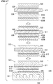
- a power module 1 according to the first embodiment of the present invention is shown in FIG. 1 .
- the power module 1 includes the power module substrate 10 and a semiconductor device 3 bonded to one surface (upper surface in FIG. 1 ) of the power module substrate 10 with a solder layer 2 interposed therebetween.
- the power module substrate 10 includes; a ceramic substrate 11 constituting an insulation layer, a circuit layer 12 (bonding body) arranged on one surface (upper surface in FIG. 1 and first surface) of the ceramic substrate 11, and a metal layer 13 arranged on the other surface (second surface) of the ceramic substrate 11.
- the ceramic substrate 11 is composed of AlN (aluminum nitride), Si 3 N 4 (silicon nitride), Al 2 O 3 (alumina), or the like, each of which has high insulation properties. In the present embodiment, it is composed of AlN which is excellent in heat dissipation properties.
- the thickness of the ceramic substrate 11 is set to be in a range of 0.2 to 1.5 mm, and in the present embodiment, the thickness thereof is set to 0.635 mm.
- the circuit layer 12 includes an Al layer 12A arranged on the first surface of the ceramic substrate 11, and a Cu layer 12B (copper member layer) laminated on one surface of the Al layer 12A with a Ti layer 15 interposed therebetween.
- the Al layer 12A is formed by bonding an aluminum plate (aluminum member) composed of aluminum or an aluminum alloy on the first surface of the ceramic substrate 11.
- the Al layer 12A is formed by bonding a rolled sheet of aluminum having a purity of 99% by mass or more (so-called 2N aluminum).
- the rolled sheet of aluminum having a purity of 99% by mass or more preferably contains Si of 0.08 to 0.95% by mass.
- the thickness of the aluminum plate is set to be in a range of 0.1 to 1.0 mm, and in the present embodiment, the thickness thereof is set to 0.4 mm.
- the copper layer 12B is formed by bonding a copper plate (metal member) composed of copper or a copper alloy on one surface (upper surface in FIG. 1 ) of the Al layer 12A with the Ti layer 15 interposed therebetween.
- the copper layer 12B is formed by bonding a rolled sheet of an oxygen-free copper to the Al layer 12A by solid phase diffusion bonding with Ti foil interposed therebetween.
- the thickness of the copper plate that will be bonded is set to be in a range of 0.1 to 6.0 mm, and in the present embodiment, the thickness thereof is set to 1.0 mm.
- the Ti layer 15 is formed by laminating the Al layer 12A and the copper plate with titanium foil interposed therebetween and bonding by solid phase diffusion bonding.
- the titanium foil has a purity of 99% or more.
- the thickness of the titanium foil is set to 3 to 40 ⁇ m, and in the present embodiment, the thickness thereof is 10 ⁇ m.
- an Al-Ti-Si layer 16 in which Si is solid-solubilized into Al 3 Ti is formed.
- the Al-Ti-Si layer 16 is formed by interdiffusion of Al atoms in the Al layer 12A and Ti atoms in the Ti layer 15.
- the thickness of the Al-Ti-Si layer 16 is set to 0.5 to 10 ⁇ m, and in the present embodiment, the thickness thereof is 3 ⁇ m.
- the Al-Ti-Si layer 16 includes a first Al-Ti-Si layer 16A formed at the Ti layer 15 side and a second Al-Ti-Si layer 16B formed at the Al layer 12A side. That is, in the bonding portion between the Al layer 12A and the Cu layer 12B, the Ti layer 15, the first Al-Ti-Si layer 16A, and the second Al-Ti-Si layer 16B are formed.
- first Al-Ti-Si layer 16A and second Al-Ti-Si layer 16B are formed of an Al-Ti-Si phase in which Si is solid-solubilized into Al 3 Ti, the Si concentration of the second Al-Ti-Si layer 16B is lower than that of the first Al-Ti-Si layer 16A.
- Si contained in the first Al-Ti-Si layer 16A and second Al-Ti-Si layer 16B is the Si that is contained in the rolled sheet of 2N aluminum as impurities, and diffused into the Al-Ti-Si layer 16 and condensed therein.
- the Si concentration of the first Al-Ti-Si layer 16A is 10 to 30 at%, and in the present embodiment, the Si concentration thereof is 20 at%.
- the Si concentration of the second Al-Ti-Si layer 16B is 1 to 10 at%, and in the present embodiment, the Si concentration thereof is 3 at%.
- the metal layer 13 is formed by bonding an aluminum plate composed of aluminum or an aluminum alloy on the second surface (lower surface in FIG. 1 ) of the ceramic substrate 11.
- the metal layer 13 is formed by bonding a rolled sheet of aluminum having a purity of 99% by mass or more (so-called 2N aluminum) to the ceramic substrate 11.
- the thickness of the aluminum plate that will be the metal layer 13 is set to be in a range of 0.1 to 3.0 mm, and in the present embodiment, the thickness thereof is set to 1.6 mm.
- the semiconductor device 3 is configured of a semiconductor material such as Si.
- the semiconductor device 3 and the circuit layer 12 are bonded together with the solder layer 2 interposed therebetween.
- the solder layer 2 is, for example, a Sn-Ag-based, Sn-Cu-based, Sn-In-based, or Sn-Ag-Cu-based solder material (so-called, lead-free solder material), and it bonds the power module substrate 10 and the semiconductor device 3 together.
- an aluminum plate 22A that will be the Al layer 12A is laminated on the first surface of the ceramic substrate 11, and a copper plate 22B that will be the Cu layer 12B is laminated further thereon with a titanium foil 25 interposed between the aluminum plate 22A and copper plate 22B.
- an aluminum plate 23 that will be the metal layer 13 is laminated (aluminum plate and copper plate lamination step S01).
- the aluminum plates 22A, 23 and the ceramic substrate 11 are laminated with an Al-Si-based brazing filler metal 26 interposed between the aluminum plate 22A and ceramic substrate 11 and between the aluminum plate 23 and ceramic substrate 11.
- the laminated body is placed in a vacuum heating furnace in a state of being pressurized (at a pressure of 1 to 35 kgf/cm 2 ) in a lamination direction, and the Al layer 12A and the metal layer 13 are formed. Also, the Al layer 12A and the titanium foil 25 are bonded by solid phase diffusion bonding and the copper plate 22B and the titanium foil 25 are bonded by solid phase diffusion bonding, and the circuit layer 12 and the metal layer 13 are formed (circuit layer and metal layer formation step S02).
- the pressure in the vacuum heating furnace is preferably set to a range of 10 -6 to 10 -3 Pa
- the heating temperature therein is preferably set to 600 to 643 °C
- the retention time is preferably set to a range of 30 to 180 minutes.
- the more preferable heating temperature is in a range of 630 to 643 °C. In the present embodiment, it was performed in the conditions of a pressure of 12 kgf/cm 2 pressured in the lamination direction, a heating temperature of 640 °C, and a retention time of 60 minutes.
- each of the surfaces of the aluminum plate 22A, the titanium foil 25, and the copper plate 22B, which will be bonded, is smoothed in advance by removing scratches thereon, and then, solid phase diffusion bonding is performed.
- the power module substrate 10 according to the present embodiment is produced.
- the semiconductor device 3 is laminated on one surface (a surface) of the circuit layer 12 with the solder material interposed therebetween, and solder joint is performed in a reduction furnace (semiconductor device bonding step S03).
- the power module 1 according to the present embodiment is produced.
- the power module 1 and the power module substrate 10 configured as above, in the bonding portion of the circuit layer 12 between the Al layer 12A and the Cu layer 12B, the Ti layer 15 and the Al-Ti-Si layer 16 are formed, and a hard layer such as an Al-Ti-Cu layer and Al-Ti layer is not formed. Therefore, when a heat cycle is applied, the occurrence of cracks in the circuit layer 12 can be prevented. Thus, in the power module 1, the bonding reliability between the semiconductor device 3 and the power module substrate 10 can be improved.
- the Si concentration of the first Al-Ti-Si layer 16A formed at the Ti layer 15 side is higher than the Si concentration of the second Al-Ti-Si layer 16B formed at the Al layer 12A side, the diffusion of Ti atoms toward the Al layer 12A is suppressed by the first Al-Ti-Si layer 16A having a high Si concentration, and the thickness of the Al-Ti-Si layer 16 can be made thin. Accordingly, by the result of making thin the thickness of the Al-Ti-Si layer 16, when the heat cycle is applied, the occurrence of cracks in the bonding portion between the Al layer 12A and the Cu layer 12B can be prevented.
- the Si concentration contained in the second Al-Ti-Si layer 16B formed at the Al layer 12A side is 1 to 10 at%, an excess diffusion of Al atoms toward the Ti layer 15 can be suppressed, and the thickness of the second Al-Ti-Si layer 16B can be made thin.
- the Si concentration contained in the first Al-Ti-Si layer 16A formed at the Ti layer 15 side is 10 to 30 at%, an excess diffusion of Ti atoms toward the Al layer 12A can be suppressed, and the thickness of the first Al-Ti-Si layer 16A can be made thin.
- the production process can facilitate and the production cost can be reduced.
- the Al layer 12A having a relatively small deformation resistance is formed on the first surface of the ceramic substrate 11, the Al layer 12A absorbs the thermal stress generated when the heat cycle is applied, and the occurrence of cracks in the ceramic substrate 11 can be prevented.
- the Cu layer 12B having a relatively large deformation resistance is formed on the one surface of the Al layer 12A, the deformation of the circuit layer 12 is suppressed when the heat cycle is applied, the deformation of a solder layer 2 that bonds the semiconductor device 3 and the circuit layer 12 together is suppressed, and the bonding reliability can be improved.
- the Cu layer 12B having a good thermal conductivity is formed to one side of the circuit layer 12, the heat from the semiconductor device 3 is spread and can be efficiently transferred toward the power module substrate 10.
- the solid phase diffusion bonding between the Al layer 12A (aluminum plate 22A) and the titanium foil 25 and between the copper plate 22B and the titanium foil 25 is performed in the conditions of pressurizing at a pressure of 1 to 35 kgf/cm 2 in the lamination direction and retaining at a temperature of 600 to 643 °C, a liquid phase is not generated at an interface between the Al layer and the Ti layer, Ti atoms are diffused into the Al layer 12A and the copper plate 22B, solid phase diffusion bonding is performed by a solid phase diffusion of Al atoms and Cu atoms diffused into the titanium foil 25, and the Al layer 12A, the titanium foil 25, and the copper plate 22B can be reliably bonded together.
- the preferable temperature of solid phase diffusion bonding is set to the above range.
- each of the surfaces of the aluminum plate 22A, the copper plate 22B, and the titanium foil 25, which will be bonded is smoothed in advance by removing scratches thereon, and then, solid phase diffusion bonding is performed. Therefore, the generation of gaps at each of the bonding interfaces is suppressed and bonding can be performed.
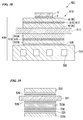
- a heat-sink-attached-power module 201 according to the second embodiment of the present invention is shown in FIG. 5 .
- the heat-sink-attached-power module 201 includes a heat-sink-attached-power module substrate 230, and a semiconductor device 3 bonded to one surface (upper surface in FIG. 5 ) of the heat-sink-attached-power module substrate 230 with a solder layer 2 interposed therebetween.
- the heat-sink-attached-power module substrate 230 includes a power module substrate 210, and a heat sink 231 (metal member) laminated to a lower side of the power module substrate 210 with a Ti layer 215 interposed therebetween.
- the power module substrate 210 includes: a ceramic substrate 11, a circuit layer 212 arranged on a first surface (upper surface in FIG. 5 ) of the ceramic substrate 11, and a metal layer 213 (Al layer) arranged on a second surface (lower surface in FIG. 5 ) of the ceramic substrate 11.
- the circuit layer 212 is formed by bonding an aluminum plate having an electrical conductivity on the first surface (upper surface in FIG. 5 ) of the ceramic substrate 11.
- the circuit layer 212 is formed by bonding a rolled sheet of aluminum having a purity of 99.99% by mass or more (so-called 4N aluminum) to the ceramic substrate 11.
- the thickness of the aluminum plate that will be bonded is set in the range of 0.1 to 1.0 mm, and in the present embodiment, the thickness thereof is set to 0.6 mm.
- the metal layer 213 is formed by bonding an aluminum plate composed of aluminum or an aluminum alloy, each of which has an electrical conductivity, on the second surface (lower surface in FIG. 5 ) of the ceramic substrate 11.
- the metal layer 213 is formed by bonding a rolled sheet of aluminum having a purity of 99% by mass or more (so-called 2N aluminum).
- the rolled sheet of aluminum having a purity of 99% by mass or more preferably contains Si of 0.08 to 0.95% by mass.
- the thickness of the aluminum plate is set in the range of 0.1 to 3.0 mm, and in the present embodiment, the thickness thereof is set to 0.6 mm.
- a heat sink 231 dissipates the heat of the power module substrate 210 side.
- the heat sink 231 is composed of copper or a copper alloy, and in the present embodiment, it is composed of oxygen-free copper.
- a flow path 232 through which a fluid for cooling flows is provided.
- the metal layer 213 and the heat sink 231 are bonded together with the Ti layer 215 interposed therebetween.
- the Ti layer 215 is formed by laminating the metal layer 213 formed of aluminum and the heat sink 231 made of copper with a titanium foil interposed therebetween and bonding by solid phase diffusion bonding.
- the titanium foil has a purity of 99% or more.
- the thickness of the titanium foil is set to 3 to 40 ⁇ m, and in the present embodiment, the thickness thereof is 10 ⁇ m.
- an Al-Ti-Si layer 216 in which Si is solid-solubilized into Al 3 Ti is formed.
- the Al-Ti-Si layer 216 is formed by interdiffusion of Al atoms in the metal layer 213 and Ti atoms in the Ti layer 215.
- the thickness of the Al-Ti-Si layer 216 is set to 0.5 to 10 ⁇ m, and in the present embodiment, the thickness thereof is 3 ⁇ m.
- the Al-Ti-Si layer 216 includes a first Al-Ti-Si layer 216A formed at the Ti layer 215 side and a second Al-Ti-Si layer 216B formed at the metal layer 213 side. That is, in the bonding portion between the metal layer 213 and the heat sink 231, the Ti layer 215, the first Al-Ti-Si layer 216A, and the second Al-Ti-Si layer 216B are formed.
- first Al-Ti-Si layer 216A and second Al-Ti-Si layer 216B are formed of an Al-Ti-Si phase in which Si is solid-solubilized into Al 3 Ti, the Si concentration of the second Al-Ti-Si layer 216B is lower than that of the first Al-Ti-Si layer 216A.
- the Si concentration of the first Al-Ti-Si layer 216A is 10 to 30 at%, and in the present embodiment, the Si concentration thereof is 20 at%.
- the Si concentration of the second Al-Ti-Si layer 216B is 1 to 10 at%, and in the present embodiment, the Si concentration thereof is 3 at%.
- an aluminum plate 222 that will be the circuit layer 212 is laminated on the first surface of the ceramic substrate 11 with an Al-Si based brazing filler metal foil 26 interposed therebetween.
- an aluminum plate 223 that will be the metal layer 213 is laminated on the second surface of the ceramic substrate 11 with an Al-Si based brazing filler metal foil 26 interposed therebetween.
- the heat sink 231 is laminated to the second surface side (lower side in FIG. 8 ) of the ceramic substrate 11 with a titanium foil 225 interposed therebetween (aluminum plate and heat sink lamination step S211).
- the laminated body is placed in a vacuum heating furnace in a state of being pressurized (at a pressure of 1 to 35 kgf/cm 2 ) in a lamination direction of the aluminum plates 222 and 223, the ceramic substrate 11, and the heat sink 231, and the circuit layer 212 and the metal layer 213 are respectively formed on the first surface and the second surface of the ceramic substrate 11.
- the metal layer 213 and the titanium foil 225 are bonded by solid phase diffusion bonding and the heat sink 231 and the titanium foil 225 are bonded by solid phase diffusion bonding, and the metal layer 213 and the heat sink 231 are bonded together (circuit layer, metal layer, heat sink bonding step S212).
- the pressure in the vacuum heating furnace is preferably set to a range of 10 -6 to 10 -3 Pa
- the heating temperature therein is preferably set to 600 to 643 °C
- the retention time is preferably set to a range of 30 to 180 minutes.
- the more preferable heating temperature is in a range of 630 to 643 °C. In the present embodiment, it was performed in the conditions of a pressure of 20 kgf/cm 2 pressured in the lamination direction, a heating temperature of 640 °C, and a retention time of 60 minutes.
- each of the surfaces of the aluminum plate 223, the titanium foil 225, and the heat sink 231, which will be bonded, is smoothed in advance by removing scratches thereon, and then, solid phase diffusion bonding is performed.
- the heat-sink-attached-power module substrate 230 and the power module substrate 210 according to the present embodiment can be obtained.
- the semiconductor device 3 is laminated on one surface of the heat-sink-attached-power module substrate 230 (circuit layer 212) with the solder material interposed therebetween, and solder joint is performed in a reduction furnace (semiconductor device bonding step S213).
- the heat-sink-attached-power module 201 is produced.
- the heat-sink-attached-power module 201 and the heat-sink-attached-power module substrate 230 configured as above, in the bonding portion between the metal layer 213 and the heat sink 231, the Ti layer 215, the Al-Ti-Si layer 216 are formed, and a hard layer such as an Al-Ti-Cu layer and Al-Ti layer is not formed. Therefore, when the heat cycle is applied, the occurrence of cracks in the bonding portion between the metal layer 213 and the heat sink 231 can be prevented. Thus, in the heat-sink-attached-power module 201, the bonding reliability between the metal layer 213 and the heat sink 231 can be improved.
- the Si concentration of the first Al-Ti-Si layer 216A formed at the Ti layer 215 side is higher than the Si concentration of the second Al-Ti-Si layer 216B formed at the metal layer 213 side, the diffusion of Ti atoms toward the metal layer 213 is suppressed by the first Al-Ti-Si layer 216A having a high Si concentration, the thickness of the Al-Ti-Si layer 216 can be made thin.
- the circuit layer 212 and the metal layer 213 are respectively formed on the first surface and second surface of the ceramic substrate 11, and furthermore, the metal layer 213 and the heat sink 231 can be bonded at the same time, the production process can facilitate and the production cost can be reduced.
- the metal layer 313 may include an Al layer 313A formed on a second surface of a ceramic substrate 11, and a Cu layer 313B bonded by solid phase diffusion bonding on a surface of the Al layer 313A that is opposite to a surface of the Al layer 313A to which the ceramic substrate 11 is bonded with a Ti layer 315 interposed between the Al layer 313A and the Cu layer 313B.
- the heat stress generated in the ceramic substrate 11 is absorbed by the Al layer 313A, and the occurrence of cracks in the ceramic substrate 11 can be prevented. Also, since the Cu layer 313B is formed at the lower side of the Al layer 313A, the heat from the semiconductor device 3 side can be effectively dissipated.
- the metal layer is formed of aluminum or an aluminum alloy; however, it is not limited thereto, and the metal layer may be formed of copper or a copper alloy.
- the second embodiment has been explained the case in which the metal layer is formed of aluminum or an aluminum alloy and the heat sink is formed of copper or a copper alloy.
- the metal layer may be formed of copper or a copper alloy and the heat sink may be formed of aluminum or an aluminum alloy.
- the circuit layer was formed by laminating the aluminum plate which will be the Al layer, by laminating the copper plate which will be the Cu layer on the aluminum plate with the titanium foil interposed therebetween, and by pressurizing and heating them; however, a lead frame (metal member) made of copper can be used instead of the copper plate.
- a heat-sink-attached-power module 501 according to the fifth embodiment of the present invention is shown in FIG. 13 .
- the heat-sink-attached-power module 501 includes a heat-sink-attached-power module substrate 530, and a semiconductor device 3 bonded to one surface (upper surface in FIG. 13 ) of the heat-sink-attached-power module substrate 530 with a solder layer 2 interposed therebetween.
- the heat-sink-attached-power module substrate 530 includes a power module substrate 510, and a heat sink 531 bonded to a lower side of the power module substrate 510 with a solder layer 535 interposed therebetween.
- the power module substrate 510 includes; a ceramic substrate 511 constituting an insulation layer, a circuit layer 512 arranged on one surface (upper surface in FIG. 14 and first surface) of the ceramic substrate 511, and a metal layer 513 arranged on the other surface (lower surface in FIG. 15 and second surface) of the ceramic substrate 511.
- the ceramic substrate 511 is composed of AlN (aluminum nitride), Si 3 N 4 (silicon nitride), Al 2 O 3 (alumina) or the like, each of which has high insulation properties. In the present embodiment, it is composed of AlN (aluminum nitride) which is excellent in heat dissipation properties.
- the thickness of the ceramic substrate 511 is set in a range of 0.2 to 1.5 mm, and in the present embodiment, the thickness thereof is set to 0.635 mm.
- the circuit layer 512 is formed by bonding an aluminum plate composed of aluminum or an aluminum alloy on the first surface (upper surface in FIG. 14 ) of the ceramic substrate 511.
- the circuit layer 512 is formed by bonding a rolled sheet of aluminum having a purity of 99% or more (so-called 2N aluminum) to the ceramic substrate 511.
- the thickness of the aluminum plate that will be the circuit layer 512 is set in a range of 0.1 to 1.0 mm, and in the present embodiment, the thickness thereof is set to 0.6 mm.
- the metal layer 513 includes an Al layer 513A arranged on the second surface (lower surface in FIG. 14 ) of the ceramic substrate 511, and a Cu layer 513B (metal member layer) laminated on a surface of the Al layer 513A that is opposite to a surface of the Al layer 513A to which the ceramic substrate 511 is bonded with a Ti layer 515 interposed between the Al layer 513A and the Cu layer 513B.
- Al layer 513A arranged on the second surface (lower surface in FIG. 14 ) of the ceramic substrate 511
- a Cu layer 513B metal member layer laminated on a surface of the Al layer 513A that is opposite to a surface of the Al layer 513A to which the ceramic substrate 511 is bonded with a Ti layer 515 interposed between the Al layer 513A and the Cu layer 513B.
- the Al layer 513A is formed by bonding an aluminum plate composed of aluminum or an aluminum alloy on the second surface of the ceramic substrate 511.
- the Al layer 513A is formed by bonding a rolled sheet of aluminum having a purity of 99% by mass or more (so-called 2N aluminum).
- the rolled sheet of aluminum having a purity of 99% by mass or more preferably contains Si of 0.08 to 0.95% by mass.
- the thickness of the aluminum plate that will be bonded is set in a range of 0.1 to 3.0 mm, and in the present embodiment, the thickness thereof is set to 0.6 mm.
- the Cu layer 513B is formed by bonding a copper plate composed of copper or a copper alloy on a surface (lower surface in FIG. 14 ) of the Al layer 513A that is opposite to a surface of the Al layer 513A on which the ceramic substrate 511 is formed with the Ti layer 515 interposed between the Al layer 513A and the Cu layer 513B.
- the Cu layer 513B is formed by bonding a rolled sheet of oxygen-free copper to the Al layer 513A by solid phase diffusion bonding with titanium foil interposed therebetween.
- the thickness of the copper plate that will be bonded is set in a range of 0.1 to 6.0 mm, and in the present embodiment, the thickness thereof is set to 0.3 mm.
- the Ti layer 515 is formed by laminating the Al layer 513A and the copper plate with a titanium foil interposed therebetween and bonding by solid phase diffusion bonding.
- the titanium foil has a purity of 99% or more.
- the thickness of the titanium foil is set to 3 to 40 ⁇ m, and in the present embodiment, the thickness thereof is 15 ⁇ m.
- an Al-Ti-Si layer 516 in which Si is solid-solubilized into Al 3 Ti is formed.
- the Al-Ti-Si layer 516 is formed by interdiffusion of Al atoms in the Al layer 512A and Ti atoms in the Ti layer 515.
- the thickness of the Al-Ti-Si layer 516 is set to 0.5 to 10 ⁇ m, and in the present embodiment, the thickness thereof is 5 ⁇ m.
- the Al-Ti-Si layer 516 includes a first Al-Ti-Si layer 516A formed at the Ti layer 515 side and a second Al-Ti-Si layer 516B formed at the Al layer 513A side. That is, in the bonding portion between the Al layer 513A and the Cu layer 513B, the Ti layer 515, the first Al-Ti-Si layer 516A, and the second Al-Ti-Si layer 516B are formed.
- first Al-Ti-Si layer 516A and second Al-Ti-Si layer 516B are formed of an Al-Ti-Si phase in which Si is solid-solubilized into Al 3 Ti, the Si concentration of the second Al-Ti-Si layer 516B is lower than the Si concentration of the first Al-Ti-Si layer 516A.
- Si contained in the first Al-Ti-Si layer 516A and the second Al-Ti-Si layer 516B is the Si that is contained in the rolled sheet of 2N aluminum as impurities, and diffused into the Al-Ti-Si layer 516 and condensed therein.
- the Si concentration of the first Al-Ti-Si layer 516A is 10 to 30 at%, and in the present embodiment, the Si concentration thereof is 20 at%.
- the Si concentration of the second Al-Ti-Si layer 516B is 1 to 10 at%, and in the present embodiment, the Si concentration thereof is 3 at%.
- the semiconductor device 3 is configured of a semiconductor material such as Si.
- the semiconductor device 3 and the circuit layer 512 are bonded together with a solder layer 2 interposed therebetween.
- the solder layer 2 is, for example, a Sn-Ag-based, Sn-Cu-based, Sn-In-based, or Sn-Ag-Cu-based solder material (so-called, lead-free solder material), and it bonds the power module substrate 510 and the semiconductor device 3 together.
- a heat sink 531 dissipates the heat of the power module substrate 510 side.
- the heat sink 531 is composed of copper or a copper alloy, and in the present embodiment, it is composed of oxygen-free copper.
- a flow path 532 through which a fluid for cooling flows is provided.
- the solder layer 535 is, for example, a Sn-Ag-based, Sn-Cu-based, Sn-In-based, or Sn-Ag-Cu-based solder material (so-called, lead-free solder material), as the same as the solder layer 2, and it bonds the power module substrate 510 and the heat sink 531 together.
- an aluminum plate 522 that will be the circuit layer 512 is laminated on the first surface of the ceramic substrate 511.
- an aluminum plate 523A that will be the Al layer 513A is laminated, and further thereon, a copper plate 523B that will be the Cu layer 513B is laminated with a titanium foil 525 interposed therebetween (aluminum plate and copper plate lamination step S501).
- the aluminum plates 522, 523A, and the ceramic substrate 511 were laminated with an Al-Si-based brazing filler metal 526 interposed between the aluminum plate 522 and ceramic substrate 511 and between the aluminum plate 523A and ceramic substrate 511.
- the laminated body is placed in a vacuum heating furnace in a state of being pressurized (at a pressure of 1 to 35 kgf/cm 2 ) in a lamination direction, and the circuit layer 512 and the Al layer 513A are formed. Also, the Al layer 513A and the titanium foil 525 are bonded by solid phase diffusion bonding, the copper plate 523B and the titanium foil 525 are bonded by solid phase diffusion bonding, and the circuit layer 512 and the metal layer 513 are formed (circuit layer and metal layer formation step S502).
- the pressure in the vacuum heating furnace is preferably set to a range of 10 -6 to 10 -3 Pa
- the heating temperature therein is preferably set to 600 to 643 °C
- the retention time is preferably set to a range of 30 to 180 minutes.
- the more preferable heating temperature is in a range of 630 to 643 °C. In the present embodiment, it was performed in the conditions of a pressure of 12 kgf/cm 2 pressured in the lamination direction, a heating temperature of 640 °C, and a retention time of 60 minutes.
- each of the surfaces of the aluminum plate 523A, the titanium foil 525, and the copper plate 523B, which will be bonded, is smoothed in advance by removing scratches thereon, and then, solid phase diffusion bonding is performed.
- the power module substrate 510 according to the present embodiment is produced.
- the heat sink 531 is laminated on the metal layer 513 of the power module substrate 510 with a solder material interposed therebetween, and solder joint is performed in a reduction furnace (heat sink bonding step S503).
- the heat-sink-attached-power module substrate 530 according to the present embodiment is produced.
- the semiconductor device 3 is laminated on one surface (a surface) of the circuit layer 512 with the solder material interposed therebetween, and solder joint is performed in a reduction furnace (semiconductor device bonding step S504).
- the heat-sink-attached-power module 501 according to the present embodiment is produced.
- the heat-sink-attached-power module 501, the heat-sink-attached-power module substrate 530, and the power module substrate 510 according to the present embodiment configured as above, in the bonding portion of the metal layer 513 between the Al layer 513A and the Cu layer 513B, the Ti layer 515 and the Al-Ti-Si layer 516 are formed, and a hard layer such as an Al-Ti-Cu layer and Al-Ti layer is not formed. Therefore, when the heat cycle is applied, the occurrence of cracks in the metal layer 513 can be prevented. Thus, the bonding reliability between the power module substrate 510 and the heat sink 531 can be improved.
- the Si concentration of the first Al-Ti-Si layer 516A formed at the Ti layer 515 side is higher than the Si concentration of the second Al-Ti-Si layer 516B formed at the Al layer 513A side, the diffusion of Ti atoms toward the Al layer 513A is suppressed by the first Al-Ti-Si layer 516A having a high Si concentration, and the thickness of the Al-Ti-Si layer 516 can be made thin. Accordingly, by the result of making thin the thickness of the Al-Ti-Si layer 516, when the heat cycle is applied, the occurrence of cracks in the bonding portion between the Al layer 513A and the Cu layer 513B can be prevented.
- the Si concentration contained in the second Al-Ti-Si layer 516B formed at the Al layer 513A side is 1 to 10 at%, an excess diffusion of Al atoms toward the Ti layer 515 can be suppressed, and the thickness of the second Al-Ti-Si layer 516B can be made thin.
- the Si concentration contained in the first Al-Ti-Si layer 516A formed at the Ti layer 515 side is 10 to 30 at%, an excess diffusion of Ti atoms toward the Al layer 513A can be suppressed, and the thickness of the first Al-Ti-Si layer 516A can be made thin.
- the production process can facilitate and the production cost can be reduced.
- the Al layer 513A having a relatively small deformation resistance is formed on the second surface of the ceramic substrate 511, the Al layer 513A absorbs the thermal stress generated when the heat cycle is applied, and the occurrence of cracks in the ceramic substrate 511 can be prevented.
- the Cu layer 513B having a relatively large deformation resistance is formed on a surface of the Al layer 513A that is opposite to a surface of the Al layer 513A on which the ceramic substrate 511 is formed, the deformation of the metal layer 513 is suppressed when the heat cycle is applied, the deformation of the solder layer 535 that bonds the metal layer 513 and the heat sink 531 together is suppressed, and the bonding reliability can be improved.
- the solid phase diffusion bonding between the Al layer 513A (aluminum plate 523A) and the titanium foil 525 and between the copper plate 523B and the titanium foil 525 is performed in the conditions of pressurizing at a pressure of 1 to 35 kgf/cm 2 in the lamination direction and retaining at a temperature of 600 to 643 °C, Ti atoms are diffused into the Al layer 513A and the copper plate 523B, solid phase diffusion bonding is performed by a solid phase diffusion of Al atoms and Cu atoms diffused into the Ti foil 525, and the Al layer 513A, the titanium foil 525, and the copper plate 523B can be reliably bonded together.
- the preferable temperature of solid phase diffusion bonding is set to the above range.
- each of the surfaces of the aluminum plate 523A, the copper plate 523B, and the titanium foil 525, which will be bonded is smoothed in advance by removing scratches thereon, and then, solid phase diffusion bonding is performed. Therefore, the generation of gaps at each of the bonding interfaces is suppressed and bonding can be performed.
- the Ni layer is formed instead of the Cu layer, a good soldering properties is obtained, and the bonding reliability can be improved when the metal layer and the heat sink are bonded together with the solder layer interposed therebetween. Furthermore, in a case where the Ni layer is formed by solid phase diffusion bonding, since a masking treatment performed in the formation of a Ni plating film by electroless plating or the like is not necessary, the production cost can be reduced. In this case, it is desirable to set the thickness of the Ni layer to 1 to 30 ⁇ m.
- the thickness of the Ni layer is less than 1 ⁇ m, effects of the improvement of the bonding reliability between the Ni layer and the semiconductor device may not be obtained, and when the thickness of thereof exceeds 30 ⁇ m, the Ni layer becomes a thermal resistance and the transfer of heat toward the heat sink may not be effectively performed.
- the solid phase diffusion bonding can performed using the same condition of the formation of the Cu layer in the first embodiment.
- the bonding reliability can be improved.
- the thickness of the Ag layer is less than 1 ⁇ m, effects of the improvement of the bonding reliability between the Ag layer and the semiconductor device may not be obtained, and when the thickness of thereof exceeds 20 ⁇ m, effects of the improvement of the bonding reliability are not exerted and it incurs an increase in cost.
- the solid phase diffusion bonding can performed using the same condition of the formation of the Cu layer in the first embodiment.
- a circuit layer 612 may include an Al layer 612A formed on a first surface (upper surface in FIG. 18 ) of a ceramic substrate 511, and a Cu layer 612B bonded by solid phase diffusion bonding on one surface (upper surface in FIG. 18 ) of the Al layer 612A with a Ti layer 615 interposed therebetween.
- the heat stress generated in the ceramic substrate 511 is absorbed by the Al layer 612A, and the occurrence of cracks in the ceramic substrate 511 can be prevented. Also, since the Cu layer 612B is formed at the upper side of the Al layer 612A, the heat from the semiconductor device 3 side is spread and can be effectively dissipated toward a heat sink 531 side.
- the first Al-Ti-Si layer and the second Al-Ti-Si layer can be formed as the same with the power module substrate 10 (510) by sequentially laminating the aluminum plate 422A (723A) composed of 4N aluminum, an Al-Si-based brazing filler metal foil 426 (726), a titanium foil 425 (725), and the copper plate 422B (723B) and by bonding them by solid phase diffusion bonding; and thus the occurrence of cracks in the circuit layer or the metal layer can be prevented when the heat cycle is applied.
- the above embodiments have been explained the cases in which the metal layer and the heat sink are bonded together with the solder material interposed therebetween; however, the bonding may be performed by other techniques.
- the bonding may be performed by the above-described silver oxide paste or a brazing filler metal foil.
- the circuit layer is formed of aluminum or an aluminum alloy; however, it is not limited thereto, and the circuit layer may be formed of copper or a copper alloy. Also, the circuit layer may be part of a lead frame formed of copper or a copper alloy.
- the embodiments have been explained the cases in which the heat sink is formed of copper or a copper alloy.
- the heat sink may be formed of aluminum or an aluminum alloy.
- the bonding body (or metal layer) was formed by laminating the aluminum plate which will be the Al layer on the first surface or the second surface of the ceramic substrate with the Al-Si-based brazing filler metal foil interposed therebetween, by further laminating the copper plate which will be the Cu layer on the aluminum plate with the titanium foil interposed therebetween, and by pressurizing and heating them; however, a clad metal made of Ti/Cu may be used instead of the titanium foil and the copper plate. Also, a clad metal made of three layers of Al/Ti/Cu may be used instead of the titanium foil and the copper plate.
- a clad metal made of Ti/Ni or a clad metal made of Al/Ti/Ni can be used.
- a clad metal made of Ti/Ag or a clad metal made of Al/Ti/Ag can be used.
- a plate (2 mm ⁇ 2 mm, and thickness of 0.3 mm) made of a metal member described in Table 1 was laminated on one surface of an aluminum plate (10 mm ⁇ 10 mm, and thickness of 0.6 mm) formed of 2N aluminum containing Si of 0.25% by mass with a titanium foil interposed therebetween, and the plate and the aluminum plate were bonded together by solid phase diffusion bonding in a condition shown in Table 1 by the methods described in the above embodiments.
- a metal member (2 mm ⁇ 2 mm, and thickness of 0.3 mm) formed of an oxygen-free copper plate was laminated on one surface of an aluminum member (10 mm ⁇ 10 mm, and thickness of 0.6 mm) formed of an aluminum plate having a purity of 99.99% or more with a titanium foil interposed therebetween, and the metal member and the aluminum member were bonded together by solid phase diffusion bonding in a condition shown in Table 1 as the same with the bonding body of Present Invention's Examples 1-1.
- a cross-sectional surface of each of the bonding bodies was carried out ion etching with conditions of an ion accelerating voltage: 5 kV; a processing time: 14 hours; and a projection amount from a masking shield: 100 ⁇ m, by using a cross-section polisher (SM-09010 produced by JEOL Ltd.), and then a bonding portion between an Al layer (aluminum member) and a metal member layer (metal member) was observed.
- SM-09010 produced by JEOL Ltd.
- a shear test was carried out on the bonding bodies and shear strength was measured. In addition, the shear test was carried out so as to comply with the standard of the International Electrotechnical Commission IEC 60749-19.
- the observation result (SEM image) of cross-sectional surface of the Present Invention's Example 1-1 was shown in FIG. 11
- the observation result (SEM image) of cross-sectional surface of the Comparative Example 1-1 was shown in FIG. 12 .
- Table 1 the presence of the Al-Ti-Si layer, and the measurement results of shear test of the bonding body were shown.
- the Al-Ti-Si layer was confirmed between the Ti layer and the Al layer (aluminum member). It was confirmed that the thickness of the Al-Ti-Si layer is formed thin. It was confirmed that such Al-Ti-Si layer is also formed in the Present Invention's Examples 1-2 to 1-7.
- Comparative Example 1-1 an Al-Ti layer was formed between the Ti layer and the Al layer, but an Al-Ti-Si layer was not confirmed. As shown in FIG. 12 , the thickness of the Al-Ti layer of the Comparative Example 1-1 is thicker than the thickness of the Al-Ti-Si layer of the Present Invention's Examples 1-1 to 1-7, and cracks were observed at the bonding interface thereof.
- the shear strength was 28 MPa
- the shear strength was 79 MPa or more and a significantly high shear strength was confirmed in the Present Invention's Examples.
- a power module of each of Present Invention's Examples 2-1 to 2-7 was produced in a following manner.
- a 2N aluminum plate (having a thickness of 0.6 mm) which contains Si of 0.25% by mass and will be an Al layer was laminated on a first surface of a ceramic substrate, and a plate made of a metal member described in Table 2 was laminated further thereon with a titanium foil interposed therebetween.
- a 4N aluminum plate (having a thickness of 0.6 mm) which has a purity of 99.99% or more and will be a metal layer was laminated on a second surface of the ceramic substrate.
- an Al-Si-based brazing filler metal foil was laminated between the aluminum plate and the ceramic substrate.
- heating treatment was carried out in a condition shown in Table 2, the Al layer and the metal layer were respectively formed on the first surface and the second surface of the ceramic substrate, and the circuit layer was formed by bonding a plate formed of the Al layer, a titanium foil, and the metal member by solid phase diffusion bonding.
- a semiconductor device was bonded to one surface of the circuit layer with a solder material interposed therebetween.
- a power module of the Comparative Example 2-1 was produced in the same manner with the power module of the Present Invention's Example 2-1 except for using a 4N aluminum having a purity of 99.99% or more as the Al layer.
- Heat cycle test was carried out by applying heat cycles that repeat from -40 to 125 °C to the power module. In the present example, 4000 cycles of the heat cycle were applied.
- the bonding rate of the interface between the Al layer and the metal member layer was measured before and after the heat cycle test.
- the bonding rate of the bonding portion between the Al layer and the metal member layer was evaluated using an ultrasonic flaw detection device, and the bonding rate was calculated from the calculating formula shown below.
- the initial bonding area was defined as a target area of bonding at the time before the bonding, that is, the area of the Al layer. Since the peeled off part is indicated by a white color part in an ultrasonic flaw detection image, the area of the white color part is defined as a peeled off area.
- Bonding rate % Initial bonding area - Peeled off area / Initial bonding area ⁇ 100
- the initial bonding rate was as high as 97.8% or more, and the bonding rate after the heat cycle test was maintained in high rate.
- the power module according to the Present Invention's Examples are high in bonding reliability.
- a heat-sink-attached-power module of each of Present Invention's Examples 3-1 to 3-5 was produced in a following manner.
- An Al (2N-Al) plate which has a purity of 99% or more and will be a circuit layer was laminated on a first surface of a ceramic substrate shown in Table 3.
- an aluminum plate which has a purity of 99% or more (and containing Si of 0.25% by mass) and will be an Al layer was laminated, and a copper plate formed of oxygen-free copper was laminated further on the aluminum plate with a titanium foil interposed therebetween.
- an Al-Si-based brazing filler metal foil was laminated between the aluminum plate and the ceramic substrate.
- the circuit layer and the Al layer were respectively formed on the first surface and the second surface of the ceramic substrate, and the metal layer was formed by bonding the Al layer, a titanium foil, and the copper plate by solid phase diffusion bonding.
- the metal layer of the power module substrate and a heat sink shown in Table 3 are bonded together using a Sn-Sb-based solder material.
- a semiconductor device was bonded to one surface of the circuit layer with a Sn-Sb-based solder material interposed therebetween.
- a production method of a heat-sink-attached-power module of each of Present Invention's Examples 3-6 to 3-8 will be explained.
- a 2N aluminum plate which contains Si of 0.25% by mass and will be an Al layer was laminated on a first surface of a ceramic substrate, and a metal plate which will be a metal member layer described in Table 3 was laminated further on the 2N aluminum plate with a titanium foil interposed therebetween.
- an aluminum plate which has a purity of 99% or more, (contains Si of 0.25% by mass,) and will be another Al layer was laminated on a second surface of the ceramic substrate, another metal plate which will be another metal member layer described in Table 3 was laminated further on the aluminum plate with a titanium foil interposed therebetween.
- an Al-Si-based brazing filler metal foil was laminated between the aluminum plate and the ceramic substrate.
- heating treatment was carried out in a condition shown in Table 3, the Al layers each were formed on the first surface and the second surface of the ceramic substrate, and each of the circuit layer and the metal layer was formed by bonding a plate formed of the Al layer, titanium foil, and the metal member by solid phase diffusion bonding.
- the metal layer of the power module substrate and a heat sink shown in Table 3 were bonded together using a Sn-Sb-based solder material.
- a semiconductor device was bonded to one surface of the circuit layer with a Sn-Sb-based solder material interposed therebetween.
- a heat-sink-attached-power module of the Comparative Example 1 was produced in the same manner with the heat-sink-attached-power module of the Present Invention's Example 3-1 except for using aluminum having a purity of 99.99% or more (4N aluminum) as the Al layer.
- heat treatment was carried out in the condition shown in Table 3.
- Thermal cycle test (heat cycle test) was carried out on the heat-sink-attached-power module, and the bonding rate between the ceramic substrate and the metal layer after the test was evaluated.
- the present invention provides a bonding body, a power module substrate, and a heat-sink-attached-power module substrate, in each of which, an aluminum member (Al layer) and a metal member (metal member layer) composed of any one of copper, nickel, and silver are satisfactorily bonded together, each of which can prevent the occurrence of cracks in the bonding portion between the aluminum member and metal member, and each of which has a good bonding reliability.
Landscapes
- Engineering & Computer Science (AREA)
- Chemical & Material Sciences (AREA)
- Mechanical Engineering (AREA)
- Materials Engineering (AREA)
- Microelectronics & Electronic Packaging (AREA)
- Physics & Mathematics (AREA)
- Condensed Matter Physics & Semiconductors (AREA)
- General Physics & Mathematics (AREA)
- Computer Hardware Design (AREA)
- Power Engineering (AREA)
- Organic Chemistry (AREA)
- Metallurgy (AREA)
- Ceramic Engineering (AREA)
- Geometry (AREA)
- Structural Engineering (AREA)
- Cooling Or The Like Of Semiconductors Or Solid State Devices (AREA)
Abstract
Description
- The present invention relates to a bonding body in which an aluminum member and a metal member composed of copper, nickel or silver are bonded together, a power module substrate, and a heat-sink-attached power module substrate.
- The present application claims priority on Japanese Patent Application No.
2013-052408 2013-052409 - In the semiconductor device such as a power module and a LED, it has a structure in which the semiconductor element is bonded onto a circuit layer composed of a conductive material.
- Since a power semiconductor device of high-power control that is used to control wind power, electric vehicles such as electric automobiles, and the like, generates a large amount of heat, as a substrate mounting the power semiconductor device, in the case where a metal plate having excellent conductivity is bonded to one surface of a ceramic substrate (insulation layer) composed of, for example AlN (aluminum nitride), or two metal plates having excellent conductivity are bonded to respective surfaces of the ceramic substrate, a power module substrate in which the metal plate disposed on one surface of the ceramic substrate is used as a circuit layer and another metal plate disposed on the other surface of the ceramic substrate is used as a metal layer has been widely used conventionally.
- For example, in the power module shown in
Patent Document 1, it has a structure including: a power module substrate in which a circuit layer (aluminum member) composed of Al and disposed on one surface of a ceramic substrate, and a metal layer composed of Al and disposed on the other surface of the ceramic substrate are formed; and a semiconductor device bonded on the circuit layer with a solder material interposed therebetween. A heat sink is bonded to the downside of the power module substrate, and the power module is configured to transfer the heat generated by the semiconductor device to the power module substrate side and to dissipate the heat to the outside via the heat sink. - As in the power module described in the
Patent Document 1, when the circuit layer is composed of Al, an oxidation coating film of Al is formed on a surface of the circuit layer, and therefore, the semiconductor device cannot be bonded by the solder material. Also, when the metal layer is composed of Al, an oxidation coating film of Al is formed on a surface of the metal layer, and therefore, the heat sink cannot be bonded by the solder material. - Conventionally, as shown in, for example,
Patent Document 2, a Ni plating film is formed on each surface of a circuit layer, metal layer and heat sink by electroless plating or the like, and then, they are bonded together by a solder material. - In addition, in
Patent Document 3, as an alternative technique using the solder material, a technique in which a semiconductor device, metal layer, heat sink and so on are bonded together using a silver oxide paste that includes silver oxide particles and a reducing agent containing an organic substance has been proposed. - Furthermore, in Patent Document 4, a power module in which each of a circuit layer and metal layer is formed by an Al layer and Cu layer has been proposed. In this case, since the Cu layer is disposed on each surface of the circuit layer and metal layer, a good bonding of the semiconductor device can be performed using the solder material. Also, since Cu has a large deformation resistance as compared with Al, when a heat cycle is applied on the power module, a great deformation of the surface of the circuit layer and the surface of the metal layer can be prevented, the occurrence of cracks in a solder layer is prevented, and the bonding reliability between the semiconductor device and the circuit layer and the bonding reliability between the metal layer and the heat sink can be improved.
- In addition, in the power module described in Patent Document 4, a bonding body in which an Al layer and Cu layer are bonded together with a Ti layer interposed therebetween is used as the circuit layer and the metal layer. Here, a diffusion layer is formed between the Al layer and Ti layer, and the diffusion layer has an Al-Ti layer, an Al-Ti-Si layer, and an Al-Ti-Cu layer such that the Al-Ti layer, Al-Ti-Si layer, and Al-Ti-Cu layer are sequentially arranged from the Al layer.
-
- [Patent Document 1] Japanese Patent No.
3171234 - [Patent Document 2] Japanese Unexamined Patent Application, First Publication No.
2004-172378 - [Patent Document 3] Japanese Unexamined Patent Application, First Publication No.
2008-208442 - [Patent Document 4] Japanese Patent Publication No.
3012835 - As described in the
Patent Document 2, in the power module substrate in which the Ni plating film is formed on the surface of the circuit layer and on the surface of the metal layer, a deterioration of the surface of the Ni plating film due to oxidation, or the like, occurs in a step that until the semiconductor device is bonded to the circuit layer and in a step that until the heat sink is bonded to the metal layer, and there was a possibility of reducing in bonding reliability between the semiconductor device and circuit layer bonded with the solder material interposed therebetween, and reducing in bonding reliability between the heat sink and metal plate bonded with the solder material interposed therebetween. Also, in order to avoid troubles such as electric corrosion that is the result of forming the Ni plating film in an undesired area, a masking treatment may be performed in the Ni plating step. In this manner, when the plating treatment is performed after performing the masking treatment, significant effort is required in the step of forming the Ni plating film on a portion of the circuit layer and on a portion of the metal layer, and thus, there is a problem in that the cost of producing the power module is increased significantly. - Furthermore, as described in the
Patent Document 3, when the circuit layer and the semiconductor device are bonded together using the silver oxide paste and when the metal layer and the heat sink are bonded together using the silver oxide paste, since the bonding properties of a sintered body formed of Al and the silver oxide paste are poor, it was necessary to form an Ag underlayer on the surface of the circuit layer and on the surface of the metal layer, in advance. - In addition, in the power module described in the Patent Document 4, a hard layer such as an Al-Ti layer and Al-Ti-Cu layer is formed at a bonding interface between an Al layer and Ti layer of the circuit layer, and another hard layer such as an Al-Ti layer and Al-Ti-Cu layer is formed at a bonding interface between an Al layer and Ti layer of the metal layer. Therefore, there was a problem in that the bonding interfaces become a starting point of cracks when a heat cycle is applied.
- Moreover, in the case where a Cu plate, or the like, is laminated on the Al layer with a Ti foil interposed therebetween and is heated at the temperature at which an interface between the Al layer and the Ti foil is melted, a liquid phase is generated at the bonding interface, and humps and a variation of thickness are generated. Therefore, there was a problem of reducing in the bonding reliability.
- Here, as an alternative of Ni plating of the
Patent Document 2, as described in the Patent Document 4, a Ni layer may be formed by bonding a Ni plate via a Ti foil on the circuit layer composed of Al and on the metal layer composed of Al. Furthermore, when the silver oxide paste of thePatent Document 3 is used, the Ag underlayer may be formed by bonding an Ag plate via the Ti foil on the circuit layer composed of Al and on the metal layer composed of Al. - However, when the Ni layer and Ag layer are formed by the method described in the Patent Document 4, as the same in the case of forming the Cu layer, there is a possibility of reducing in bonding reliability by reason of the formation of a hard layer such as an Al-Ti layer, an Al-Ti-Ni layer, and an Al-Ti-Ag layer formed at the bonding interface between the Al layer and the Ti layer, humps generated at the bonding interface, and the like.
- As above, conventionally, a good bonding of the aluminum member and the metal member composed of any one of copper, nickel, and silver could not be achieved, and a bonding body having an excellent bonding reliability could not be obtained. Also, conventionally, a good bonding of the Al layer and the metal member layer composed of any one of Cu, Ni, and Ag could not be achieved, and a power module substrate having the metal layer which is excellent in bonding reliability could not be obtained.
- The present invention has been made in view of the above circumstances, and the purpose thereof is to provide: a bonding body, a power module substrate, and a heat-sink-attached-power module substrate, in each of which, an aluminum member and the metal member composed of any one of copper, nickel, and silver are satisfactorily bonded together, each of which can prevent the occurrence of cracks in a bonding portion, and each of which has a good bonding reliability.
- Also, in a metal layer having an Al layer and a metal member layer composed of any one of copper, nickel, and silver, the purpose the present invention is to provide: a power module substrate and a heat-sink-attached-power module substrate, in each of which the Al layer and the metal layer member are satisfactory bonded together, each of which can prevent the occurrence of cracks in a bonding portion, and each of which has a good bonding reliability.
- In order to solve the above problems, (1) an aspect of the present invention provides a bonding body including: an aluminum member composed of aluminum; and a metal member composed of any one of copper, nickel, and silver, wherein the aluminum member and the metal member are bonded together. In a bonding portion between the aluminum member and the metal member, a Ti layer and an Al-Ti-Si layer are formed, the Ti layer being disposed at the metal member side; and the Al-Ti-Si layer being disposed between the Ti layer and the aluminum member and containing Si which is solid-solubilized into Al3Ti. The Al-Ti-Si layer includes: a first Al-Ti-Si layer formed at the Ti layer side; and a second Al-Ti-Si layer formed at the aluminum member side and a Si concentration of which is lower than a Si concentration of the first Al-Ti-Si layer.
- According to the above bonding body, in the bonding interface between the aluminum member composed of aluminum and the metal member composed of any one of copper, nickel, and silver, the Ti layer and the Al-Ti-Si layer are formed, and a hard layer such as an Al-Ti-Cu layer and Al-Ti layer is not formed. Therefore, when the heat cycle is applied, the occurrence of cracks at the bonding portion is prevented and the bonding reliability between the aluminum member and the metal member can be improved.
- Furthermore, since the first Al-Ti-Si layer formed at the Ti layer side has a Si concentration higher than that of the second Al-Ti-Si layer formed at the aluminum member side, the diffusion of Ti atoms toward the aluminum member is suppressed by the first Al-Ti-Si layer having a high Si concentration, the thickness of the first Al-Ti-Si layer and second Al-Ti-Si layer can be made thin, and when the heat cycle is applied, the occurrence of cracks in the bonding portion can be prevented.
- In addition, in the present invention, aluminum is composed of pure aluminum or an aluminum alloy, and the metal member is composed of any one of: copper or a copper alloy; nickel or a nickel alloy; and silver or a silver alloy.
- (2) Another aspect of the present invention provides the bonding body described in (1), wherein a Si concentration contained in the second Al-Ti-Si layer is 1 at% or more in the bonding body.
In this case, since the second Al-Ti-Si layer formed at the aluminum member side has a sufficient Si concentration, an excess diffusion of Al atoms composing the aluminum member toward the Ti layer can be suppressed, and the thickness of the first Al-Ti-Si layer and second Al-Ti-Si layer can be made thin. - (3) Still another aspect of the present invention provides a power module substrate including: an insulation layer; and a circuit layer formed on one surface of the insulation layer, wherein the circuit layer is formed of the bonding body described in (1) or (2). The circuit layer includes: an Al layer formed of the aluminum member and formed on one surface of the insulation layer, and a metal member layer formed of the metal member and formed on one surface of the Al layer. In a bonding portion between the Al layer and the metal member layer, a Ti layer and an Al-Ti-Si layer are formed, the Ti layer being disposed at the metal member layer side, and the Al-Ti-Si layer being disposed between the Ti layer and the Al layer and containing Si which is solid-solubilized into Al3Ti. The Al-Ti-Si layer includes: a first Al-Ti-Si layer formed at the Ti layer side; and a second Al-Ti-Si layer formed at the Al layer side and a Si concentration of which is lower than a Si concentration of the first Al-Ti-Si layer.
- According to the above power module substrate, in the circuit layer, in the bonding portion between the Al layer and the metal member layer, the Ti layer and the Al-Ti-Si layer are formed, and a hard layer such as an Al-Ti-Cu layer and Al-Ti layer is not formed. Therefore, when the heat cycle is applied, the occurrence of cracks in the circuit layer can be prevented. Thus, in the power module, the bonding reliability between the semiconductor device and the power module substrate can be improved.
- Furthermore, since the Si concentration of the first Al-Ti-Si layer formed at the Ti layer side is higher than the Si concentration of the second Al-Ti-Si layer formed at the Al layer side, the diffusion of Ti atoms toward the Al layer is suppressed, the thickness of the first Al-Ti-Si layer and second Al-Ti-Si layer can be made thin.
- In addition, in this case, since the Al layer having a relatively small deformation resistance is formed on the one surface of the insulation layer, the Al layer absorbs the thermal stress generated when the heat cycle is applied, and the occurrence of cracks in the ceramic substrate can be prevented.
- Furthermore, in the case where the Cu layer composed of copper or a copper alloy is formed on one surface of the Al layer, since the Cu layer has a large deformation resistance as compared with the Al layer, when the heat cycle is applied, the deformation of the circuit layer is prevented, the deformation of the solder layer bonding the semiconductor device and the circuit layer together is prevented, and the bonding reliability can be improved. Also, since the Cu layer having a good thermal conductivity is formed at one side of the circuit layer, the heat from the semiconductor device is spread and can be efficiently transferred toward the power module substrate.
- Also, in the case where a Ni layer composed of nickel or a nickel alloy is formed on the one surface of the Al layer, good soldering properties are obtained and the bonding reliability between the semiconductor device and the Ni layer improves.
- Also, in the case where an Ag layer composed of silver or a silver alloy is formed on the one surface of the Al layer, since the bonding of the Ag layer and the silver which is derived by reduction of silver oxide is a bonding performed by the same type of metal when the semiconductor device is bonded by using, for example, a silver oxide paste including silver oxide particles and a reducing agent containing an organic substance, the bonding reliability can be improved. In addition, since the Ag layer having a good thermal conductivity is formed at one side of the circuit layer, the heat from the semiconductor device is spread and can be efficiently transferred toward the power module substrate.
- (4) Still another aspect of the present invention provides the power module substrate described in (3), and the power module substrate further includes: a metal layer formed on the other surface of the insulation layer, wherein the metal layer is formed of the bonding body described in (1) or (2). The metal layer includes: an Al layer formed of the aluminum member and formed on the other surface of the insulation layer, and a metal member layer formed on a surface of the Al layer that is opposite to a surface of the Al layer on which the insulation layer is formed, and formed of the metal member. In a bonding portion between the Al layer and the metal member layer, a Ti layer and an Al-Ti-Si layer are formed, the Ti layer being disposed at the metal member layer side, and the Al-Ti-Si layer being disposed between the Ti layer and the Al layer and containing Si which is solid-solubilized into Al3Ti. The Al-Ti-Si layer includes: a first Al-Ti-Si layer formed at the Ti layer side; and a second Al-Ti-Si layer formed at the Al layer side and a Si concentration of which is lower than a Si concentration of the first Al-Ti-Si layer.
- In this case, in the metal layer, in the bonding portion between the Al layer and the metal member layer, the Ti layer and the first Al-Ti-Si layer are formed, and a hard layer such as an Al-Ti-Cu layer and Al-Ti layer is not formed. Therefore, when the heat cycle is applied, the occurrence of cracks in the metal layer can be prevented. Thus, when the metal layer and the heat sink are bonded together, the bonding reliability between the metal layer and the heat sink can be improved.
- (5) Still another aspect of the present invention provides a power module substrate including: an insulation layer; a circuit layer formed on one surface of the insulation layer; and a metal layer formed on the other surface of the insulation layer, wherein the metal layer is formed of the bonding body described in (1) or (2). In a bonding portion between an Al layer formed of the aluminum member and a metal member layer formed of the metal member, a Ti layer and an Al-Ti-Si layer are formed, the Ti layer being disposed at the metal member layer side, and the Al-Ti-Si layer being disposed between the Ti layer and the Al layer and containing Si which is solid-solubilized into Al3Ti. The Al-Ti-Si layer includes: a first Al-Ti-Si layer formed at the Ti side; and a second Al-Ti-Si layer formed at the Al layer side and a Si concentration of which is lower than a Si concentration of the first Al-Ti-Si layer.
- In addition, in the present invention, aluminum is composed of pure aluminum or an aluminum alloy, copper is composed of pure copper or a copper alloy, nickel is composed of pure nickel or a nickel alloy, and silver is composed of pure silver or a silver alloy.
- According to the above power module substrate, in the metal layer, in the bonding interface between the Al layer and the metal member layer, the Ti layer and the Al-Ti-Si layer are formed, and a hard layer such as an Al-Ti-Cu layer and Al-Ti layer is not formed. Therefore, when the heat cycle is applied, the occurrence of cracks in the metal layer can be prevented. Thus, when the metal layer of the power module substrate is bonded to the heat sink, the bonding reliability between the power module substrate and the heat sink can be improved.
- Furthermore, since the Si concentration of the first Al-Ti-Si layer formed at the Ti layer side is higher than the Si concentration of the second Al-Ti-Si layer formed at the Al layer side, the diffusion of Ti atoms toward the Al layer is suppressed, the thickness of the first Al-Ti-Si layer and second Al-Ti-Si layer can be made thin.
- Also, in this case, since the Al layer having a relatively small deformation resistance is formed on the other surface of the insulation layer, the Al layer absorbs the thermal stress generated when the heat cycle is applied, and the occurrence of cracks in the ceramic substrate is suppressed.
- Furthermore, in the case where the Cu layer composed of copper or a copper alloy is formed on a surface of the Al layer that is opposite to a surface of the Al layer on which the insulation layer is formed, since the Cu layer has a large deformation resistance as compared with the Al layer, when the heat cycle is applied, the deformation of the metal layer is suppressed and the deformation of a bonding layer in which the heat sink and the metal layer are bonded together is suppressed, and thus, the bonding reliability can be improved.
- Also, in the case where a Ni layer composed of nickel or a nickel alloy is formed on a surface of the Al layer that is opposite to the surface of the Al layer on which the insulation layer is formed, good soldering properties are obtained and the bonding reliability of the heat sink and the Ni layer is improved.
- Also, in the case where an Ag layer composed of silver or a silver alloy is formed on a surface of the Al layer that is opposite to a surface of the Al layer on which the insulation layer is formed, since the bonding of the Ag layer and the silver which is derived by reduction of silver oxide is a bonding performed by the same type of metal when the heat sink is bonded using, for example, a silver oxide paste including an silver oxide particles and a reducing agent containing an organic substance, the bonding reliability can be improved.
-
- (6) Still another aspect of the present invention provides a heat-sink-attached power module substrate including: the power module substrate described in any one of (3) to (5), and a heat sink bonded to the metal layer.
According to the above heat-sink-attached power module substrate, since the power module substrate and the heat sink are bonded together, the heat from the power module substrate can be efficiently dissipated via the heat sink. - (7) Still another aspect of the present invention provides the heat-sink-attached power module substrate described in (6), and the metal layer and the heat sink are bonded together through a solder layer.
In this case, since a metal member layer that is composed of copper, nickel or silver and is formed at a side close to the heat sink in the metal layer and the heat sink are bonded together through the solder layer, the metal member layer and the solder layer are satisfactorily bonded together and the bonding reliability between the metal layer and the heat sink can be improved. -
- (8) Still another aspect of the present invention provides a heat-sink-attached power module substrate including: an insulation layer; and a circuit layer formed on one surface of the insulation layer, a metal layer formed on the other surface of the insulation layer, and a heat sink bonded on the metal layer, wherein the metal layer and the heat sink are formed of the bonding body described in (1) or (2). One of the metal layer and the heat sink of the bonding surface is formed of aluminum, and the other of the metal layer and the heat sink of the bonding surface is formed of any one of copper, nickel and silver. In a bonding portion between the metal layer and the heat sink, a Ti layer and an Al-Ti-Si layer are formed, the Ti layer being disposed at the metal layer side when the metal layer of the bonding surface is formed of any one of copper, nickel and silver or being disposed at the heat sink side when the heat sink of the bonding surface is formed of any one of copper, nickel and silver, and the Al-Ti-Si layer being disposed between the Ti layer and the metal layer when the metal layer of the bonding surface is composed of aluminum or being disposed between the Ti layer and the heat sink when the heat sink of the bonding surface is composed of aluminum, and containing Si which is solid-solubilized into Al3Ti. The Al-Ti-Si layer includes: a first Al-Ti-Si layer formed at the Ti side; and a second Al-Ti-Si layer formed at the metal layer side when the metal layer of the bonding surface is composed of aluminum or formed at the heat sink side when the heat sink of the bonding surface is composed of aluminum, and a Si concentration of which is lower than a Si concentration of the first Al-Ti-Si layer.
- According to the above heat-sink-attached-power module substrate, in the bonding portion between the metal layer and the heat sink, the Ti layer and the Al-Ti-Si layer are formed, and a hard layer such as an Al-Ti-Cu layer and Al-Ti layer is not formed. Therefore, when the heat cycle is applied, the occurrence of cracks in the bonding portion between the metal layer and the heat sink can be prevented, and the bonding reliability can be improved.
- The present invention provides a bonding body, a power module substrate, and a heat-sink-attached-power module substrate, in each of which, an aluminum member (Al layer) and a metal member (metal member layer) composed of any one of copper, nickel, and silver are satisfactorily bonded together, each of which can prevent the occurrence of cracks in the bonding portion between the aluminum member and metal member, and each of which has a good bonding reliability.
-
-
FIG. 1 is a schematic explanatory diagram of a power module according to a first embodiment of the present invention. -
FIG. 2 is an enlarged view of a bonding interface between an Al layer and a Ti layer inFIG. 1 . -
FIG. 3 is a flow chart explaining a production method of a power module according to the first embodiment of the present invention. -
FIG. 4 is a schematic explanatory diagram of a production method of the power module according to the first embodiment of the present invention. -
FIG. 5 is a schematic explanatory diagram of a heat-sink-attached-power module according to a second embodiment of the present invention. -
FIG. 6 is an enlarged view of a bonding interface between a metal layer and a Ti layer inFIG. 5 . -
FIG. 7 is a flow chart explaining a production method of a heat-sink-attached-power module according to the second embodiment of the present invention. -
FIG. 8 is a schematic explanatory diagram of a producing method of the heat-sink-attached-power module according to the second embodiment of the present invention. -
FIG. 9 is a schematic explanatory diagram of a power module according to a third embodiment of the present invention. -
FIG. 10 is a schematic explanatory diagram of a production method of the power module according to a fourth embodiment of the present invention. -
FIG. 11 is a SEM picture of the bonding portion between an aluminum member and a copper member in a bonding body of the Present Invention's Example 1-1. -
FIG. 12 is a SEM picture of the bonding portion between an aluminum member and a copper member in a bonding body of the Comparative Example 1-1. -
FIG. 13 is a schematic explanatory diagram of a heat-sink-attached-power module according to a fifth embodiment of the present invention. -
FIG. 14 is a schematic explanatory diagram of a power module substrate according to the fifth embodiment of the present invention. -
FIG. 15 is an enlarged view of a bonding portion between a Ti layer and an Al layer in a metal layer inFIG. 14 . -
FIG. 16 is a flow chart explaining a production method of a heat-sink-attached-power module according to the fifth embodiment of the present invention. -
FIG. 17 is a schematic explanatory diagram of a production method of the heat-sink-attached-power module according to the fifth embodiment of the present invention. -
FIG. 18 is a schematic explanatory diagram of a heat-sink-attached-power module according to a sixth embodiment of the present invention. -
FIG. 19 is a schematic explanatory diagram of a production method of the power module substrate according to a seventh embodiment of the present invention. - Embodiments of the present invention will be explained below with reference to the accompanying drawings. First, a first embodiment of the present invention is explained.
- A
power module 1 according to the first embodiment of the present invention is shown inFIG. 1 . - The
power module 1 includes thepower module substrate 10 and asemiconductor device 3 bonded to one surface (upper surface inFIG. 1 ) of thepower module substrate 10 with asolder layer 2 interposed therebetween. - The
power module substrate 10 includes; aceramic substrate 11 constituting an insulation layer, a circuit layer 12 (bonding body) arranged on one surface (upper surface inFIG. 1 and first surface) of theceramic substrate 11, and ametal layer 13 arranged on the other surface (second surface) of theceramic substrate 11. - The
ceramic substrate 11 is composed of AlN (aluminum nitride), Si3N4 (silicon nitride), Al2O3 (alumina), or the like, each of which has high insulation properties. In the present embodiment, it is composed of AlN which is excellent in heat dissipation properties. The thickness of theceramic substrate 11 is set to be in a range of 0.2 to 1.5 mm, and in the present embodiment, the thickness thereof is set to 0.635 mm. - As shown in
FIG. 1 , thecircuit layer 12 includes anAl layer 12A arranged on the first surface of theceramic substrate 11, and aCu layer 12B (copper member layer) laminated on one surface of theAl layer 12A with aTi layer 15 interposed therebetween. - The
Al layer 12A is formed by bonding an aluminum plate (aluminum member) composed of aluminum or an aluminum alloy on the first surface of theceramic substrate 11. In the present embodiment, theAl layer 12A is formed by bonding a rolled sheet of aluminum having a purity of 99% by mass or more (so-called 2N aluminum). The rolled sheet of aluminum having a purity of 99% by mass or more preferably contains Si of 0.08 to 0.95% by mass. In addition, the thickness of the aluminum plate is set to be in a range of 0.1 to 1.0 mm, and in the present embodiment, the thickness thereof is set to 0.4 mm. - The
copper layer 12B is formed by bonding a copper plate (metal member) composed of copper or a copper alloy on one surface (upper surface inFIG. 1 ) of theAl layer 12A with theTi layer 15 interposed therebetween. In the present embodiment, thecopper layer 12B is formed by bonding a rolled sheet of an oxygen-free copper to theAl layer 12A by solid phase diffusion bonding with Ti foil interposed therebetween. In addition, the thickness of the copper plate that will be bonded is set to be in a range of 0.1 to 6.0 mm, and in the present embodiment, the thickness thereof is set to 1.0 mm. - The
Ti layer 15 is formed by laminating theAl layer 12A and the copper plate with titanium foil interposed therebetween and bonding by solid phase diffusion bonding. Here, the titanium foil has a purity of 99% or more. In addition, the thickness of the titanium foil is set to 3 to 40 µm, and in the present embodiment, the thickness thereof is 10 µm. - As shown in
FIG. 2 , at a bonding interface between theAl layer 12A and theTi layer 15, an Al-Ti-Si layer 16 in which Si is solid-solubilized into Al3Ti is formed. - The Al-Ti-
Si layer 16 is formed by interdiffusion of Al atoms in theAl layer 12A and Ti atoms in theTi layer 15. The thickness of the Al-Ti-Si layer 16 is set to 0.5 to 10 µm, and in the present embodiment, the thickness thereof is 3 µm. - As shown in
FIG. 2 , the Al-Ti-Si layer 16 includes a first Al-Ti-Si layer 16A formed at theTi layer 15 side and a second Al-Ti-Si layer 16B formed at theAl layer 12A side. That is, in the bonding portion between theAl layer 12A and theCu layer 12B, theTi layer 15, the first Al-Ti-Si layer 16A, and the second Al-Ti-Si layer 16B are formed. - These first Al-Ti-
Si layer 16A and second Al-Ti-Si layer 16B are formed of an Al-Ti-Si phase in which Si is solid-solubilized into Al3Ti, the Si concentration of the second Al-Ti-Si layer 16B is lower than that of the first Al-Ti-Si layer 16A. In addition, in the present embodiment, Si contained in the first Al-Ti-Si layer 16A and second Al-Ti-Si layer 16B is the Si that is contained in the rolled sheet of 2N aluminum as impurities, and diffused into the Al-Ti-Si layer 16 and condensed therein. - The Si concentration of the first Al-Ti-
Si layer 16A is 10 to 30 at%, and in the present embodiment, the Si concentration thereof is 20 at%. The Si concentration of the second Al-Ti-Si layer 16B is 1 to 10 at%, and in the present embodiment, the Si concentration thereof is 3 at%. - The
metal layer 13 is formed by bonding an aluminum plate composed of aluminum or an aluminum alloy on the second surface (lower surface inFIG. 1 ) of theceramic substrate 11. In the present embodiment, themetal layer 13 is formed by bonding a rolled sheet of aluminum having a purity of 99% by mass or more (so-called 2N aluminum) to theceramic substrate 11. In addition, the thickness of the aluminum plate that will be themetal layer 13 is set to be in a range of 0.1 to 3.0 mm, and in the present embodiment, the thickness thereof is set to 1.6 mm. - The
semiconductor device 3 is configured of a semiconductor material such as Si. Thesemiconductor device 3 and thecircuit layer 12 are bonded together with thesolder layer 2 interposed therebetween. - The
solder layer 2 is, for example, a Sn-Ag-based, Sn-Cu-based, Sn-In-based, or Sn-Ag-Cu-based solder material (so-called, lead-free solder material), and it bonds thepower module substrate 10 and thesemiconductor device 3 together. - Next, a production method of the
power module 1 according to the present embodiment will be explained with reference toFIGS. 3 and4 . - First, as shown in
FIG. 4 , analuminum plate 22A that will be theAl layer 12A is laminated on the first surface of theceramic substrate 11, and acopper plate 22B that will be theCu layer 12B is laminated further thereon with atitanium foil 25 interposed between thealuminum plate 22A andcopper plate 22B. On the second surface of theceramic substrate 11, analuminum plate 23 that will be themetal layer 13 is laminated (aluminum plate and copper plate lamination step S01). Here, in the present embodiment, thealuminum plates ceramic substrate 11 are laminated with an Al-Si-basedbrazing filler metal 26 interposed between thealuminum plate 22A andceramic substrate 11 and between thealuminum plate 23 andceramic substrate 11. - Next, the laminated body is placed in a vacuum heating furnace in a state of being pressurized (at a pressure of 1 to 35 kgf/cm2) in a lamination direction, and the
Al layer 12A and themetal layer 13 are formed. Also, theAl layer 12A and thetitanium foil 25 are bonded by solid phase diffusion bonding and thecopper plate 22B and thetitanium foil 25 are bonded by solid phase diffusion bonding, and thecircuit layer 12 and themetal layer 13 are formed (circuit layer and metal layer formation step S02). - Here, the pressure in the vacuum heating furnace is preferably set to a range of 10-6 to 10-3 Pa, the heating temperature therein is preferably set to 600 to 643 °C, and the retention time is preferably set to a range of 30 to 180 minutes. The more preferable heating temperature is in a range of 630 to 643 °C. In the present embodiment, it was performed in the conditions of a pressure of 12 kgf/cm2 pressured in the lamination direction, a heating temperature of 640 °C, and a retention time of 60 minutes.
- In addition, each of the surfaces of the
aluminum plate 22A, thetitanium foil 25, and thecopper plate 22B, which will be bonded, is smoothed in advance by removing scratches thereon, and then, solid phase diffusion bonding is performed. - In the above manner, the
power module substrate 10 according to the present embodiment is produced. - Next, the
semiconductor device 3 is laminated on one surface (a surface) of thecircuit layer 12 with the solder material interposed therebetween, and solder joint is performed in a reduction furnace (semiconductor device bonding step S03). - In the above manner, the
power module 1 according to the present embodiment is produced. - According to the
power module 1 and thepower module substrate 10 according to the present embodiment configured as above, in the bonding portion of thecircuit layer 12 between theAl layer 12A and theCu layer 12B, theTi layer 15 and the Al-Ti-Si layer 16 are formed, and a hard layer such as an Al-Ti-Cu layer and Al-Ti layer is not formed. Therefore, when a heat cycle is applied, the occurrence of cracks in thecircuit layer 12 can be prevented. Thus, in thepower module 1, the bonding reliability between thesemiconductor device 3 and thepower module substrate 10 can be improved. - Furthermore, since the Si concentration of the first Al-Ti-
Si layer 16A formed at theTi layer 15 side is higher than the Si concentration of the second Al-Ti-Si layer 16B formed at theAl layer 12A side, the diffusion of Ti atoms toward theAl layer 12A is suppressed by the first Al-Ti-Si layer 16A having a high Si concentration, and the thickness of the Al-Ti-Si layer 16 can be made thin. Accordingly, by the result of making thin the thickness of the Al-Ti-Si layer 16, when the heat cycle is applied, the occurrence of cracks in the bonding portion between theAl layer 12A and theCu layer 12B can be prevented. - Also, since the Si concentration contained in the second Al-Ti-
Si layer 16B formed at theAl layer 12A side is 1 to 10 at%, an excess diffusion of Al atoms toward theTi layer 15 can be suppressed, and the thickness of the second Al-Ti-Si layer 16B can be made thin. - Moreover, since the Si concentration contained in the first Al-Ti-
Si layer 16A formed at theTi layer 15 side is 10 to 30 at%, an excess diffusion of Ti atoms toward theAl layer 12A can be suppressed, and the thickness of the first Al-Ti-Si layer 16A can be made thin. - Also, in the present embodiment, since the
aluminum plate 22A, thetitanium foil 25, thecopper plate 22B, and thealuminum plate 23 are bonded at one time on the first surface and second surface of theceramic substrate 11, the production process can facilitate and the production cost can be reduced. - In addition, since the
Al layer 12A having a relatively small deformation resistance is formed on the first surface of theceramic substrate 11, theAl layer 12A absorbs the thermal stress generated when the heat cycle is applied, and the occurrence of cracks in theceramic substrate 11 can be prevented. - Furthermore, since the
Cu layer 12B having a relatively large deformation resistance is formed on the one surface of theAl layer 12A, the deformation of thecircuit layer 12 is suppressed when the heat cycle is applied, the deformation of asolder layer 2 that bonds thesemiconductor device 3 and thecircuit layer 12 together is suppressed, and the bonding reliability can be improved. - Also, since the
Cu layer 12B having a good thermal conductivity is formed to one side of thecircuit layer 12, the heat from thesemiconductor device 3 is spread and can be efficiently transferred toward thepower module substrate 10. - In the present embodiment, the solid phase diffusion bonding between the
Al layer 12A (aluminum plate 22A) and thetitanium foil 25 and between thecopper plate 22B and thetitanium foil 25 is performed in the conditions of pressurizing at a pressure of 1 to 35 kgf/cm2 in the lamination direction and retaining at a temperature of 600 to 643 °C, a liquid phase is not generated at an interface between the Al layer and the Ti layer, Ti atoms are diffused into theAl layer 12A and thecopper plate 22B, solid phase diffusion bonding is performed by a solid phase diffusion of Al atoms and Cu atoms diffused into thetitanium foil 25, and theAl layer 12A, thetitanium foil 25, and thecopper plate 22B can be reliably bonded together. - In a case where a pressure applied to the laminated body in the lamination direction is less than 1 kgf/cm2 in performing of solid phase diffusion bonding, a sufficient bonding of the
Al layer 12A, thetitanium foil 25, and thecopper plate 22B together becomes difficult, and a gap may cause at the bonding interfaces. In addition, in a case where a pressure applied thereto exceeds 35 kgf/cm2, since the applied pressure is too high, cracks may occur in theceramic substrate 11. For such reasons, the applied pressure in performing of solid phase diffusion bonding is set to the above range. - In a case where the temperature in performing of solid phase diffusion bonding is 600°C or more, the diffusion of Al atoms, Ti atoms, and Cu atoms are promoted, and sufficient solid phase diffusion can be performed in a short amount of time. In addition, in a case where the temperature is 643°C or less, a generation of humps at the bonding interfaces by a generation of a liquid phase caused by melting of aluminum; and a thickness variation, can be suppressed. Thus, the preferable temperature of solid phase diffusion bonding is set to the above range.
- In addition, in a case where there are scratches on the surface on which bonding will be performed when solid phase diffusion bonding is performed, a gap may occur when solid phase diffusion bonding is performed. However, in the present embodiment, each of the surfaces of the
aluminum plate 22A, thecopper plate 22B, and thetitanium foil 25, which will be bonded, is smoothed in advance by removing scratches thereon, and then, solid phase diffusion bonding is performed. Therefore, the generation of gaps at each of the bonding interfaces is suppressed and bonding can be performed. - Next, a second embodiment of the present invention will be explained. In addition, with respect to the same configurations as the first embodiment, the same reference numerals are used and the detail explanations thereof are omitted.
- A heat-sink-attached-
power module 201 according to the second embodiment of the present invention is shown inFIG. 5 . The heat-sink-attached-power module 201 includes a heat-sink-attached-power module substrate 230, and asemiconductor device 3 bonded to one surface (upper surface inFIG. 5 ) of the heat-sink-attached-power module substrate 230 with asolder layer 2 interposed therebetween. - The heat-sink-attached-
power module substrate 230 includes apower module substrate 210, and a heat sink 231 (metal member) laminated to a lower side of thepower module substrate 210 with aTi layer 215 interposed therebetween. - As shown in
FIG. 5 , thepower module substrate 210 includes: aceramic substrate 11, acircuit layer 212 arranged on a first surface (upper surface inFIG. 5 ) of theceramic substrate 11, and a metal layer 213 (Al layer) arranged on a second surface (lower surface inFIG. 5 ) of theceramic substrate 11. - The
circuit layer 212 is formed by bonding an aluminum plate having an electrical conductivity on the first surface (upper surface inFIG. 5 ) of theceramic substrate 11. In the present embodiment, thecircuit layer 212 is formed by bonding a rolled sheet of aluminum having a purity of 99.99% by mass or more (so-called 4N aluminum) to theceramic substrate 11. In addition, the thickness of the aluminum plate that will be bonded is set in the range of 0.1 to 1.0 mm, and in the present embodiment, the thickness thereof is set to 0.6 mm. - The
metal layer 213 is formed by bonding an aluminum plate composed of aluminum or an aluminum alloy, each of which has an electrical conductivity, on the second surface (lower surface inFIG. 5 ) of theceramic substrate 11. In the present embodiment, themetal layer 213 is formed by bonding a rolled sheet of aluminum having a purity of 99% by mass or more (so-called 2N aluminum). The rolled sheet of aluminum having a purity of 99% by mass or more preferably contains Si of 0.08 to 0.95% by mass. In addition, the thickness of the aluminum plate is set in the range of 0.1 to 3.0 mm, and in the present embodiment, the thickness thereof is set to 0.6 mm. - A
heat sink 231 dissipates the heat of thepower module substrate 210 side. Theheat sink 231 is composed of copper or a copper alloy, and in the present embodiment, it is composed of oxygen-free copper. In theheat sink 231, aflow path 232 through which a fluid for cooling flows is provided. - In addition, the
metal layer 213 and theheat sink 231 are bonded together with theTi layer 215 interposed therebetween. - The
Ti layer 215 is formed by laminating themetal layer 213 formed of aluminum and theheat sink 231 made of copper with a titanium foil interposed therebetween and bonding by solid phase diffusion bonding. Here, the titanium foil has a purity of 99% or more. In addition, the thickness of the titanium foil is set to 3 to 40 µm, and in the present embodiment, the thickness thereof is 10 µm. - As shown in
FIG. 6 , at a bonding interface between themetal layer 213 and theTi layer 215, an Al-Ti-Si layer 216 in which Si is solid-solubilized into Al3Ti is formed. - The Al-Ti-
Si layer 216 is formed by interdiffusion of Al atoms in themetal layer 213 and Ti atoms in theTi layer 215. The thickness of the Al-Ti-Si layer 216 is set to 0.5 to 10 µm, and in the present embodiment, the thickness thereof is 3 µm. As shown inFIG. 6 , the Al-Ti-Si layer 216 includes a first Al-Ti-Si layer 216A formed at theTi layer 215 side and a second Al-Ti-Si layer 216B formed at themetal layer 213 side. That is, in the bonding portion between themetal layer 213 and theheat sink 231, theTi layer 215, the first Al-Ti-Si layer 216A, and the second Al-Ti-Si layer 216B are formed. - These first Al-Ti-
Si layer 216A and second Al-Ti-Si layer 216B are formed of an Al-Ti-Si phase in which Si is solid-solubilized into Al3Ti, the Si concentration of the second Al-Ti-Si layer 216B is lower than that of the first Al-Ti-Si layer 216A. - The Si concentration of the first Al-Ti-
Si layer 216A is 10 to 30 at%, and in the present embodiment, the Si concentration thereof is 20 at%. The Si concentration of the second Al-Ti-Si layer 216B is 1 to 10 at%, and in the present embodiment, the Si concentration thereof is 3 at%. - Next, a production method of the heat-sink-attached-
power module 201 and the heat-sink-attached-power module substrate 230 according to the present embodiment will be explained with reference toFIG. 7 andFIG. 8 . - First, as shown in
FIG. 8 , analuminum plate 222 that will be thecircuit layer 212 is laminated on the first surface of theceramic substrate 11 with an Al-Si based brazingfiller metal foil 26 interposed therebetween. Also, analuminum plate 223 that will be themetal layer 213 is laminated on the second surface of theceramic substrate 11 with an Al-Si based brazingfiller metal foil 26 interposed therebetween. Theheat sink 231 is laminated to the second surface side (lower side inFIG. 8 ) of theceramic substrate 11 with atitanium foil 225 interposed therebetween (aluminum plate and heat sink lamination step S211). - Next, the laminated body is placed in a vacuum heating furnace in a state of being pressurized (at a pressure of 1 to 35 kgf/cm2) in a lamination direction of the
aluminum plates ceramic substrate 11, and theheat sink 231, and thecircuit layer 212 and themetal layer 213 are respectively formed on the first surface and the second surface of theceramic substrate 11. Also, themetal layer 213 and thetitanium foil 225 are bonded by solid phase diffusion bonding and theheat sink 231 and thetitanium foil 225 are bonded by solid phase diffusion bonding, and themetal layer 213 and theheat sink 231 are bonded together (circuit layer, metal layer, heat sink bonding step S212). - Here, the pressure in the vacuum heating furnace is preferably set to a range of 10-6 to 10-3 Pa, the heating temperature therein is preferably set to 600 to 643 °C, and the retention time is preferably set to a range of 30 to 180 minutes. The more preferable heating temperature is in a range of 630 to 643 °C. In the present embodiment, it was performed in the conditions of a pressure of 20 kgf/cm2 pressured in the lamination direction, a heating temperature of 640 °C, and a retention time of 60 minutes.
- In addition, each of the surfaces of the
aluminum plate 223, thetitanium foil 225, and theheat sink 231, which will be bonded, is smoothed in advance by removing scratches thereon, and then, solid phase diffusion bonding is performed. - In the above manner, the heat-sink-attached-
power module substrate 230 and thepower module substrate 210 according to the present embodiment can be obtained. - Next, the
semiconductor device 3 is laminated on one surface of the heat-sink-attached-power module substrate 230 (circuit layer 212) with the solder material interposed therebetween, and solder joint is performed in a reduction furnace (semiconductor device bonding step S213). - In the above manner, the heat-sink-attached-
power module 201 according to the present embodiment is produced. - According to the heat-sink-attached-
power module 201 and the heat-sink-attached-power module substrate 230 according to the present embodiment configured as above, in the bonding portion between themetal layer 213 and theheat sink 231, theTi layer 215, the Al-Ti-Si layer 216 are formed, and a hard layer such as an Al-Ti-Cu layer and Al-Ti layer is not formed. Therefore, when the heat cycle is applied, the occurrence of cracks in the bonding portion between themetal layer 213 and theheat sink 231 can be prevented. Thus, in the heat-sink-attached-power module 201, the bonding reliability between themetal layer 213 and theheat sink 231 can be improved. - Furthermore, since the Si concentration of the first Al-Ti-
Si layer 216A formed at theTi layer 215 side is higher than the Si concentration of the second Al-Ti-Si layer 216B formed at themetal layer 213 side, the diffusion of Ti atoms toward themetal layer 213 is suppressed by the first Al-Ti-Si layer 216A having a high Si concentration, the thickness of the Al-Ti-Si layer 216 can be made thin. - Also, in the present embodiment, since the
circuit layer 212 and themetal layer 213 are respectively formed on the first surface and second surface of theceramic substrate 11, and furthermore, themetal layer 213 and theheat sink 231 can be bonded at the same time, the production process can facilitate and the production cost can be reduced. - As shown in
FIG. 9 (third embodiment), themetal layer 313 may include anAl layer 313A formed on a second surface of aceramic substrate 11, and a Cu layer 313B bonded by solid phase diffusion bonding on a surface of theAl layer 313A that is opposite to a surface of theAl layer 313A to which theceramic substrate 11 is bonded with aTi layer 315 interposed between theAl layer 313A and the Cu layer 313B. - In the power module 301 provided with the
metal layer 313, when the heat cycle is applied, the heat stress generated in theceramic substrate 11 is absorbed by theAl layer 313A, and the occurrence of cracks in theceramic substrate 11 can be prevented. Also, since the Cu layer 313B is formed at the lower side of theAl layer 313A, the heat from thesemiconductor device 3 side can be effectively dissipated. - In addition, the first embodiment has been explained the case in which the metal layer is formed of aluminum or an aluminum alloy; however, it is not limited thereto, and the metal layer may be formed of copper or a copper alloy.
- Also, the second embodiment has been explained the case in which the metal layer is formed of aluminum or an aluminum alloy and the heat sink is formed of copper or a copper alloy. However, they are not limited thereto, and the metal layer may be formed of copper or a copper alloy and the heat sink may be formed of aluminum or an aluminum alloy.
- In the first embodiment, the circuit layer was formed by laminating the aluminum plate which will be the Al layer, by laminating the copper plate which will be the Cu layer on the aluminum plate with the titanium foil interposed therebetween, and by pressurizing and heating them; however, a lead frame (metal member) made of copper can be used instead of the copper plate.
- A heat-sink-attached-
power module 501 according to the fifth embodiment of the present invention is shown inFIG. 13 . - The heat-sink-attached-
power module 501 includes a heat-sink-attached-power module substrate 530, and asemiconductor device 3 bonded to one surface (upper surface inFIG. 13 ) of the heat-sink-attached-power module substrate 530 with asolder layer 2 interposed therebetween. - The heat-sink-attached-
power module substrate 530 includes apower module substrate 510, and aheat sink 531 bonded to a lower side of thepower module substrate 510 with asolder layer 535 interposed therebetween. - As shown in
FIG. 14 , thepower module substrate 510 includes; aceramic substrate 511 constituting an insulation layer, acircuit layer 512 arranged on one surface (upper surface inFIG. 14 and first surface) of theceramic substrate 511, and ametal layer 513 arranged on the other surface (lower surface inFIG. 15 and second surface) of theceramic substrate 511. - The
ceramic substrate 511 is composed of AlN (aluminum nitride), Si3N4 (silicon nitride), Al2O3 (alumina) or the like, each of which has high insulation properties. In the present embodiment, it is composed of AlN (aluminum nitride) which is excellent in heat dissipation properties. The thickness of theceramic substrate 511 is set in a range of 0.2 to 1.5 mm, and in the present embodiment, the thickness thereof is set to 0.635 mm. - The
circuit layer 512 is formed by bonding an aluminum plate composed of aluminum or an aluminum alloy on the first surface (upper surface inFIG. 14 ) of theceramic substrate 511. In the present embodiment, thecircuit layer 512 is formed by bonding a rolled sheet of aluminum having a purity of 99% or more (so-called 2N aluminum) to theceramic substrate 511. In addition, the thickness of the aluminum plate that will be thecircuit layer 512 is set in a range of 0.1 to 1.0 mm, and in the present embodiment, the thickness thereof is set to 0.6 mm. - As shown in
FIG. 13 , themetal layer 513 includes anAl layer 513A arranged on the second surface (lower surface inFIG. 14 ) of theceramic substrate 511, and aCu layer 513B (metal member layer) laminated on a surface of theAl layer 513A that is opposite to a surface of theAl layer 513A to which theceramic substrate 511 is bonded with aTi layer 515 interposed between theAl layer 513A and theCu layer 513B. - The
Al layer 513A is formed by bonding an aluminum plate composed of aluminum or an aluminum alloy on the second surface of theceramic substrate 511. In the present embodiment, theAl layer 513A is formed by bonding a rolled sheet of aluminum having a purity of 99% by mass or more (so-called 2N aluminum). The rolled sheet of aluminum having a purity of 99% by mass or more preferably contains Si of 0.08 to 0.95% by mass. In addition, the thickness of the aluminum plate that will be bonded is set in a range of 0.1 to 3.0 mm, and in the present embodiment, the thickness thereof is set to 0.6 mm. - The
Cu layer 513B is formed by bonding a copper plate composed of copper or a copper alloy on a surface (lower surface inFIG. 14 ) of theAl layer 513A that is opposite to a surface of theAl layer 513A on which theceramic substrate 511 is formed with theTi layer 515 interposed between theAl layer 513A and theCu layer 513B. In the present embodiment, theCu layer 513B is formed by bonding a rolled sheet of oxygen-free copper to theAl layer 513A by solid phase diffusion bonding with titanium foil interposed therebetween. - In addition, the thickness of the copper plate that will be bonded is set in a range of 0.1 to 6.0 mm, and in the present embodiment, the thickness thereof is set to 0.3 mm.
- The
Ti layer 515 is formed by laminating theAl layer 513A and the copper plate with a titanium foil interposed therebetween and bonding by solid phase diffusion bonding. Here, the titanium foil has a purity of 99% or more. In addition, the thickness of the titanium foil is set to 3 to 40 µm, and in the present embodiment, the thickness thereof is 15 µm. - As shown in
FIG. 15 , at a bonding interface between theAl layer 513A and theTi layer 515, an Al-Ti-Si layer 516 in which Si is solid-solubilized into Al3Ti is formed. - The Al-Ti-
Si layer 516 is formed by interdiffusion of Al atoms in the Al layer 512A and Ti atoms in theTi layer 515. The thickness of the Al-Ti-Si layer 516 is set to 0.5 to 10 µm, and in the present embodiment, the thickness thereof is 5 µm. - As shown in
FIG. 15 , the Al-Ti-Si layer 516 includes a first Al-Ti-Si layer 516A formed at theTi layer 515 side and a second Al-Ti-Si layer 516B formed at theAl layer 513A side. That is, in the bonding portion between theAl layer 513A and theCu layer 513B, theTi layer 515, the first Al-Ti-Si layer 516A, and the second Al-Ti-Si layer 516B are formed. - These first Al-Ti-
Si layer 516A and second Al-Ti-Si layer 516B are formed of an Al-Ti-Si phase in which Si is solid-solubilized into Al3Ti, the Si concentration of the second Al-Ti-Si layer 516B is lower than the Si concentration of the first Al-Ti-Si layer 516A. In addition, in the present embodiment, Si contained in the first Al-Ti-Si layer 516A and the second Al-Ti-Si layer 516B is the Si that is contained in the rolled sheet of 2N aluminum as impurities, and diffused into the Al-Ti-Si layer 516 and condensed therein. - The Si concentration of the first Al-Ti-
Si layer 516A is 10 to 30 at%, and in the present embodiment, the Si concentration thereof is 20 at%. The Si concentration of the second Al-Ti-Si layer 516B is 1 to 10 at%, and in the present embodiment, the Si concentration thereof is 3 at%. - The
semiconductor device 3 is configured of a semiconductor material such as Si. Thesemiconductor device 3 and thecircuit layer 512 are bonded together with asolder layer 2 interposed therebetween. - The
solder layer 2 is, for example, a Sn-Ag-based, Sn-Cu-based, Sn-In-based, or Sn-Ag-Cu-based solder material (so-called, lead-free solder material), and it bonds thepower module substrate 510 and thesemiconductor device 3 together. - A
heat sink 531 dissipates the heat of thepower module substrate 510 side. Theheat sink 531 is composed of copper or a copper alloy, and in the present embodiment, it is composed of oxygen-free copper. In theheat sink 531, aflow path 532 through which a fluid for cooling flows is provided. - The
solder layer 535 is, for example, a Sn-Ag-based, Sn-Cu-based, Sn-In-based, or Sn-Ag-Cu-based solder material (so-called, lead-free solder material), as the same as thesolder layer 2, and it bonds thepower module substrate 510 and theheat sink 531 together. - Next, a production method of the heat-sink-attached-
power module 501 according to the present embodiment will be explained with reference toFIGS. 16 and17 . - First, as shown in
FIG. 17 , analuminum plate 522 that will be thecircuit layer 512 is laminated on the first surface of theceramic substrate 511. On the second surface of theceramic substrate 511, analuminum plate 523A that will be theAl layer 513A is laminated, and further thereon, acopper plate 523B that will be theCu layer 513B is laminated with atitanium foil 525 interposed therebetween (aluminum plate and copper plate lamination step S501). Here, in the present embodiment, thealuminum plates ceramic substrate 511 were laminated with an Al-Si-basedbrazing filler metal 526 interposed between thealuminum plate 522 andceramic substrate 511 and between thealuminum plate 523A andceramic substrate 511. - Next, the laminated body is placed in a vacuum heating furnace in a state of being pressurized (at a pressure of 1 to 35 kgf/cm2) in a lamination direction, and the
circuit layer 512 and theAl layer 513A are formed. Also, theAl layer 513A and thetitanium foil 525 are bonded by solid phase diffusion bonding, thecopper plate 523B and thetitanium foil 525 are bonded by solid phase diffusion bonding, and thecircuit layer 512 and themetal layer 513 are formed (circuit layer and metal layer formation step S502). - Here, the pressure in the vacuum heating furnace is preferably set to a range of 10-6 to 10-3 Pa, the heating temperature therein is preferably set to 600 to 643 °C, and the retention time is preferably set to a range of 30 to 180 minutes. The more preferable heating temperature is in a range of 630 to 643 °C. In the present embodiment, it was performed in the conditions of a pressure of 12 kgf/cm2 pressured in the lamination direction, a heating temperature of 640 °C, and a retention time of 60 minutes.
- In addition, each of the surfaces of the
aluminum plate 523A, thetitanium foil 525, and thecopper plate 523B, which will be bonded, is smoothed in advance by removing scratches thereon, and then, solid phase diffusion bonding is performed. - In the above manner, the
power module substrate 510 according to the present embodiment is produced. - Next, the
heat sink 531 is laminated on themetal layer 513 of thepower module substrate 510 with a solder material interposed therebetween, and solder joint is performed in a reduction furnace (heat sink bonding step S503). - In this manner, the heat-sink-attached-
power module substrate 530 according to the present embodiment is produced. - Next, the
semiconductor device 3 is laminated on one surface (a surface) of thecircuit layer 512 with the solder material interposed therebetween, and solder joint is performed in a reduction furnace (semiconductor device bonding step S504). - In the above manner, the heat-sink-attached-
power module 501 according to the present embodiment is produced. - According to the heat-sink-attached-
power module 501, the heat-sink-attached-power module substrate 530, and thepower module substrate 510 according to the present embodiment configured as above, in the bonding portion of themetal layer 513 between theAl layer 513A and theCu layer 513B, theTi layer 515 and the Al-Ti-Si layer 516 are formed, and a hard layer such as an Al-Ti-Cu layer and Al-Ti layer is not formed. Therefore, when the heat cycle is applied, the occurrence of cracks in themetal layer 513 can be prevented. Thus, the bonding reliability between thepower module substrate 510 and theheat sink 531 can be improved. - Furthermore, since the Si concentration of the first Al-Ti-
Si layer 516A formed at theTi layer 515 side is higher than the Si concentration of the second Al-Ti-Si layer 516B formed at theAl layer 513A side, the diffusion of Ti atoms toward theAl layer 513A is suppressed by the first Al-Ti-Si layer 516A having a high Si concentration, and the thickness of the Al-Ti-Si layer 516 can be made thin. Accordingly, by the result of making thin the thickness of the Al-Ti-Si layer 516, when the heat cycle is applied, the occurrence of cracks in the bonding portion between theAl layer 513A and theCu layer 513B can be prevented. - Also, since the Si concentration contained in the second Al-Ti-
Si layer 516B formed at theAl layer 513A side is 1 to 10 at%, an excess diffusion of Al atoms toward theTi layer 515 can be suppressed, and the thickness of the second Al-Ti-Si layer 516B can be made thin. - Moreover, since the Si concentration contained in the first Al-Ti-
Si layer 516A formed at theTi layer 515 side is 10 to 30 at%, an excess diffusion of Ti atoms toward theAl layer 513A can be suppressed, and the thickness of the first Al-Ti-Si layer 516A can be made thin. - Also, in the present embodiment, since the
aluminum plate 523A, thetitanium foil 525, thecopper plate 523B, and thealuminum plate 522 are bonded at one time on the first surface and second surface of theceramic substrate 511, the production process can facilitate and the production cost can be reduced. - Further, since the
Al layer 513A having a relatively small deformation resistance is formed on the second surface of theceramic substrate 511, theAl layer 513A absorbs the thermal stress generated when the heat cycle is applied, and the occurrence of cracks in theceramic substrate 511 can be prevented. - Furthermore, since the
Cu layer 513B having a relatively large deformation resistance is formed on a surface of theAl layer 513A that is opposite to a surface of theAl layer 513A on which theceramic substrate 511 is formed, the deformation of themetal layer 513 is suppressed when the heat cycle is applied, the deformation of thesolder layer 535 that bonds themetal layer 513 and theheat sink 531 together is suppressed, and the bonding reliability can be improved. - Also, in the present embodiment, the solid phase diffusion bonding between the
Al layer 513A (aluminum plate 523A) and thetitanium foil 525 and between thecopper plate 523B and thetitanium foil 525 is performed in the conditions of pressurizing at a pressure of 1 to 35 kgf/cm2 in the lamination direction and retaining at a temperature of 600 to 643 °C, Ti atoms are diffused into theAl layer 513A and thecopper plate 523B, solid phase diffusion bonding is performed by a solid phase diffusion of Al atoms and Cu atoms diffused into theTi foil 525, and theAl layer 513A, thetitanium foil 525, and thecopper plate 523B can be reliably bonded together. - In a case where a pressure applied to the lamination in the lamination direction is less than 1 kgf/cm2 in performing of solid phase diffusion bonding, a sufficient bonding of the
Al layer 513A, thetitanium foil 525, and thecopper plate 523B together becomes difficult, and a gap may cause at the bonding interfaces. In addition, in a case where a pressure applied thereto exceeds 35 kgf/cm2, since the applied pressure is too high, cracks may occur in theceramic substrate 511. For such reasons, the applied pressure in performing of solid phase diffusion bonding is set to the above range. - In a case where the temperature in performing of solid phase diffusion bonding is 600°C or more, the diffusion of Al atoms, Ti atoms, and Cu atoms are promoted, and sufficient solid phase diffusion can be performed in a short amount of time. In addition, in a case where the temperature is 643°C or less, a generation of humps at the bonding interfaces by a generation of a liquid phase caused by melting of aluminum; and a thickness variation, can be suppressed. Thus, the preferable temperature of solid phase diffusion bonding is set to the above range.
- In addition, in a case where there are scratches on the surface on which bonding will be performed when solid phase diffusion bonding is performed, a gap may occur when solid phase diffusion bonding is performed. However, in the present embodiment, each of the surfaces of the
aluminum plate 523A, thecopper plate 523B, and thetitanium foil 525, which will be bonded, is smoothed in advance by removing scratches thereon, and then, solid phase diffusion bonding is performed. Therefore, the generation of gaps at each of the bonding interfaces is suppressed and bonding can be performed. - The embodiments of the present invention have been explained as above; however, the present invention is not limited thereto and can be appropriately changed without departing from the technical concept of the present invention.
- The above embodiments have been explained in that the Al layer and the Cu layer are bonded together; however, a Ni layer composed of nickel or a nickel alloy, or an Ag layer composed of silver or a silver alloy may be bonded thereto instead of the Cu layer.
- For example, in a case where the Ni layer is formed instead of the Cu layer, a good soldering properties is obtained, and the bonding reliability can be improved when the metal layer and the heat sink are bonded together with the solder layer interposed therebetween. Furthermore, in a case where the Ni layer is formed by solid phase diffusion bonding, since a masking treatment performed in the formation of a Ni plating film by electroless plating or the like is not necessary, the production cost can be reduced. In this case, it is desirable to set the thickness of the Ni layer to 1 to 30 µm. When the thickness of the Ni layer is less than 1 µm, effects of the improvement of the bonding reliability between the Ni layer and the semiconductor device may not be obtained, and when the thickness of thereof exceeds 30 µm, the Ni layer becomes a thermal resistance and the transfer of heat toward the heat sink may not be effectively performed.
- Also, when the Ni layer is formed by solid phase diffusion bonding, the solid phase diffusion bonding can performed using the same condition of the formation of the Cu layer in the first embodiment.
- Also, in a case where the Ag layer is formed instead of the Cu layer, since the bonding of the Ag layer and the silver which is derived by reduction of silver oxide is a bonding performed by the same type of metal when the heat sink is bonded by using, for example, a silver oxide paste including silver oxide particles and a reducing agent containing an organic substance, the bonding reliability can be improved. In this case, it is desirable to set the thickness of the Ag layer to 1 to 20 µm. When the thickness of the Ag layer is less than 1 µm, effects of the improvement of the bonding reliability between the Ag layer and the semiconductor device may not be obtained, and when the thickness of thereof exceeds 20 µm, effects of the improvement of the bonding reliability are not exerted and it incurs an increase in cost.
- Also, when the Ag layer is formed by solid phase diffusion bonding, the solid phase diffusion bonding can performed using the same condition of the formation of the Cu layer in the first embodiment.
- As shown in
FIG. 18 (sixth embodiment), acircuit layer 612 may include anAl layer 612A formed on a first surface (upper surface inFIG. 18 ) of aceramic substrate 511, and aCu layer 612B bonded by solid phase diffusion bonding on one surface (upper surface inFIG. 18 ) of theAl layer 612A with aTi layer 615 interposed therebetween. - In the
power module 601 provided with thecircuit layer 612, when the heat cycle is applied, the heat stress generated in theceramic substrate 511 is absorbed by theAl layer 612A, and the occurrence of cracks in theceramic substrate 511 can be prevented. Also, since theCu layer 612B is formed at the upper side of theAl layer 612A, the heat from thesemiconductor device 3 side is spread and can be effectively dissipated toward aheat sink 531 side. - In addition, the above present embodiments have been explained the cases in which the aluminum plate composed of 2N aluminum and the copper plate composed of oxygen-free copper are laminated and bonded by solid phase diffusion bonding with the titanium foil interposed therebetween. However, in a case where an aluminum plate composed of 4N aluminum having a less content of Si than that in 2N aluminum and a copper plate are bonded together by solid phase diffusion bonding with the titanium foil interposed therebetween, an Al-Ti-Si layer in which Si is solid-solubilized in the Al3Ti is not formed at the bonding interface thereof, and an Al3Ti layer (Al-Ti layer) grows thick. When the aluminum plate composed of 4N aluminum and the copper plate are bonded together, as shown in, for example,
FIG. 10 (fourth embodiment) andFIG. 19 (seventh embodiment), the first Al-Ti-Si layer and the second Al-Ti-Si layer can be formed as the same with the power module substrate 10 (510) by sequentially laminating thealuminum plate 422A (723A) composed of 4N aluminum, an Al-Si-based brazing filler metal foil 426 (726), a titanium foil 425 (725), and thecopper plate 422B (723B) and by bonding them by solid phase diffusion bonding; and thus the occurrence of cracks in the circuit layer or the metal layer can be prevented when the heat cycle is applied. - Also, the above embodiments have been explained the cases in which the metal layer and the heat sink are bonded together with the solder material interposed therebetween; however, the bonding may be performed by other techniques. For example, the bonding may be performed by the above-described silver oxide paste or a brazing filler metal foil.
- In addition, the above embodiments have been explained the cases in which the circuit layer is formed of aluminum or an aluminum alloy; however, it is not limited thereto, and the circuit layer may be formed of copper or a copper alloy. Also, the circuit layer may be part of a lead frame formed of copper or a copper alloy.
- Also, the embodiments have been explained the cases in which the heat sink is formed of copper or a copper alloy. However, it is not limited thereto, and the heat sink may be formed of aluminum or an aluminum alloy.
- Also, the above embodiments have been explained the cases in which an aluminum plate and another aluminum plate are respectively bonded to the first surface and the second surface of the ceramic substrate with the Al-Si-based brazing filler metal foil interposed therebetween; however, it is not limited thereto, and the method of Transient Liquid Phase Bonding may be applied.
- In the above embodiments, the bonding body (or metal layer) was formed by laminating the aluminum plate which will be the Al layer on the first surface or the second surface of the ceramic substrate with the Al-Si-based brazing filler metal foil interposed therebetween, by further laminating the copper plate which will be the Cu layer on the aluminum plate with the titanium foil interposed therebetween, and by pressurizing and heating them; however, a clad metal made of Ti/Cu may be used instead of the titanium foil and the copper plate. Also, a clad metal made of three layers of Al/Ti/Cu may be used instead of the titanium foil and the copper plate.
- In a case where the Ni layer is formed instead of the Cu layer, a clad metal made of Ti/Ni or a clad metal made of Al/Ti/Ni can be used.
- In a case where the Ag layer is formed instead of the Cu layer, a clad metal made of Ti/Ag or a clad metal made of Al/Ti/Ag can be used.
- Hereinafter, the result of the confirmation experiment which was performed to confirm the effects of the present invention is explained.
- As a bonding body of each of Present Invention's Examples 1-1 to 1-7, as shown in Table 1, a plate (2 mm × 2 mm, and thickness of 0.3 mm) made of a metal member described in Table 1 was laminated on one surface of an aluminum plate (10 mm × 10 mm, and thickness of 0.6 mm) formed of 2N aluminum containing Si of 0.25% by mass with a titanium foil interposed therebetween, and the plate and the aluminum plate were bonded together by solid phase diffusion bonding in a condition shown in Table 1 by the methods described in the above embodiments.
- As a bonding body of Comparative Example 1-1, a metal member (2 mm × 2 mm, and thickness of 0.3 mm) formed of an oxygen-free copper plate was laminated on one surface of an aluminum member (10 mm × 10 mm, and thickness of 0.6 mm) formed of an aluminum plate having a purity of 99.99% or more with a titanium foil interposed therebetween, and the metal member and the aluminum member were bonded together by solid phase diffusion bonding in a condition shown in Table 1 as the same with the bonding body of Present Invention's Examples 1-1.
- Observation of cross-sectional surface of the bonding bodies and shear test were carried out on the bonding bodies obtained as above.
- A cross-sectional surface of each of the bonding bodies was carried out ion etching with conditions of an ion accelerating voltage: 5 kV; a processing time: 14 hours; and a projection amount from a masking shield: 100 µm, by using a cross-section polisher (SM-09010 produced by JEOL Ltd.), and then a bonding portion between an Al layer (aluminum member) and a metal member layer (metal member) was observed. Also, chemical composition analysis of the bonding portion was carried out using an analyzer of EPMA (electron probe microanalysis), and the presence of the formation of an Al-Ti-Si layer in which Si is solid-solubilized into Al3Ti at a bonding interface between a Ti layer and an Al layer (interface between the Ti layer and the aluminum member in
FIGS. 11 and 12 ) was checked. - A shear test was carried out on the bonding bodies and shear strength was measured. In addition, the shear test was carried out so as to comply with the standard of the International Electrotechnical Commission IEC 60749-19.
- As one example of the observation result of cross-sectional surface, the observation result (SEM image) of cross-sectional surface of the Present Invention's Example 1-1 was shown in
FIG. 11 , and the observation result (SEM image) of cross-sectional surface of the Comparative Example 1-1 was shown inFIG. 12 . Also, in Table 1, the presence of the Al-Ti-Si layer, and the measurement results of shear test of the bonding body were shown. - The bonding body in which the Al-Ti-Si layer can be confirmed from the above method was recorded as "Present" in Table; whereas, the bonding body in which the Al-Ti-Si layer cannot be confirmed was recorded as "None".
[Table 1] Aluminum member Metal member Conditions of Solid-Solubilized Bonding Presence of Al-Ti-Si layer Shear Strength Temperature [°C] Time [minute] MPa Present Invention's Example 1-1 2N aluminum Oxygen-free copper 600 60 Present 83 Present Invention's Example 1-2 2N aluminum Oxygen- free copper 610 60 Present 84 Present Invention's Example 1-3 2N aluminum Oxygen- free copper 630 120 Present 86 Present Invention's Example 1-4 2N aluminum Oxygen-free copper 640 30 Present 85 Present Invention's Example 1-5 2N aluminum Oxygen-free copper 640 180 Present 84 Present Invention's Example 1-6 2N aluminum Nickel 640 90 Present 81 Present Invention's Example 1-7 2N aluminum Silver 640 90 Present 79 Comparative Example 1-1 4N aluminum Oxygen-free copper 640 30 None 28 - In the Present Invention's Example 1-1, as shown in
FIG. 11 , the Al-Ti-Si layer was confirmed between the Ti layer and the Al layer (aluminum member). It was confirmed that the thickness of the Al-Ti-Si layer is formed thin. It was confirmed that such Al-Ti-Si layer is also formed in the Present Invention's Examples 1-2 to 1-7. - On the other hand, in Comparative Example 1-1, an Al-Ti layer was formed between the Ti layer and the Al layer, but an Al-Ti-Si layer was not confirmed. As shown in
FIG. 12 , the thickness of the Al-Ti layer of the Comparative Example 1-1 is thicker than the thickness of the Al-Ti-Si layer of the Present Invention's Examples 1-1 to 1-7, and cracks were observed at the bonding interface thereof. - Also, in the Comparative Example 1-1 in which the Al-Ti-Si layer was not confirmed, the shear strength was 28 MPa, whereas in the Present Invention's Examples 1-1 to 1-7 in which the Al-Ti-Si layer was confirmed, the shear strength was 79 MPa or more and a significantly high shear strength was confirmed in the Present Invention's Examples.
- A power module of each of Present Invention's Examples 2-1 to 2-7 was produced in a following manner. A 2N aluminum plate (having a thickness of 0.6 mm) which contains Si of 0.25% by mass and will be an Al layer was laminated on a first surface of a ceramic substrate, and a plate made of a metal member described in Table 2 was laminated further thereon with a titanium foil interposed therebetween. Also, a 4N aluminum plate (having a thickness of 0.6 mm) which has a purity of 99.99% or more and will be a metal layer was laminated on a second surface of the ceramic substrate. Here, an Al-Si-based brazing filler metal foil was laminated between the aluminum plate and the ceramic substrate. Next, heating treatment was carried out in a condition shown in Table 2, the Al layer and the metal layer were respectively formed on the first surface and the second surface of the ceramic substrate, and the circuit layer was formed by bonding a plate formed of the Al layer, a titanium foil, and the metal member by solid phase diffusion bonding. A semiconductor device was bonded to one surface of the circuit layer with a solder material interposed therebetween.
- A power module of the Comparative Example 2-1 was produced in the same manner with the power module of the Present Invention's Example 2-1 except for using a 4N aluminum having a purity of 99.99% or more as the Al layer.
- In addition, heating treatment was carried out in the condition shown in Table 2.
- In the bonding portion between the Al layer and the metal member layer of the circuit layer of the power module produced in the above manner, as the same with the Example 1, the presence of an Al-Ti-Si layer was checked. The sample in which the Al-Ti-Si layer is confirmed by the same method in the Example 1 was recorded as "Present" in the Table; whereas, the sample in which the Al-Ti-Si layer cannot be confirmed was recorded as "None" in the Table. Furthermore, heat cycle test was carried out on the power modules, and a bonding rate of the bonding portion between the Al layer and the metal member layer after the test was measured. Also, an initial bonding rate (bonding rate before heat cycle test) of the bonding portion between the Al layer and the metal member layer was measured. The heat cycle test and the measurement of the bonding rate were carried out as below.
- Heat cycle test was carried out by applying heat cycles that repeat from -40 to 125 °C to the power module. In the present example, 4000 cycles of the heat cycle were applied.
- The bonding rate of the interface between the Al layer and the metal member layer was measured before and after the heat cycle test.
- With respect to the power module before and after the heat cycle test, the bonding rate of the bonding portion between the Al layer and the metal member layer was evaluated using an ultrasonic flaw detection device, and the bonding rate was calculated from the calculating formula shown below. Here, the initial bonding area was defined as a target area of bonding at the time before the bonding, that is, the area of the Al layer. Since the peeled off part is indicated by a white color part in an ultrasonic flaw detection image, the area of the white color part is defined as a peeled off area.

- The evaluation results of the above are shown in Table 2.
[Table 2] Aluminum member Metal member Conditions of Solid-Solubilized Bonding Presence of Al-Ti-Si layer Initial Bonding Rate Bonding Rate after Heat cycle test Temperature [°C] Time [minute] % % Present Invention's Example 2-1 2N aluminum Oxygen-free copper 600 30 Present 98.2 93.8 Present Invention's Example 2-2 2N aluminum Oxygen-free copper 620 30 Present 100 96.3 Present Invention's Example 2-3 2N aluminum Oxygen- free copper 630 60 Present 99.1 98.4 Present Invention's Example 2-4 2N aluminum Oxygen-free copper 640 30 Present 100 99.5 Present Invention's Example 2-5 2N aluminum Oxygen-free copper 640 180 Present 100 99.8 Present Invention's Example 2-6 2N aluminum Nickel 640 120 Present 97.8 97.3 Present Invention's Example 2-7 2N aluminum Silver 640 120 Present 98.5 96.4 Comparative Example 2-1 4N aluminum Oxygen-free copper 640 30 None 72.5 8.4 - In the Comparative Example 2-1 in which an Al-Ti-Si layer was not confirmed, the initial bonding rate was as low as 72.5%, and the bonding rate significantly decreased after the heat cycle test.
- On the other hand, in the Present Invention's Examples 2-1 to 2-7 in which an Al-Ti-Si layer was confirmed, the initial bonding rate was as high as 97.8% or more, and the bonding rate after the heat cycle test was maintained in high rate. Thus, it was confirmed that the power module according to the Present Invention's Examples are high in bonding reliability.
- Hereinafter, the result of the confirmation experiment which was performed to confirm the effects of the present invention is explained.
- A heat-sink-attached-power module of each of Present Invention's Examples 3-1 to 3-5 was produced in a following manner. An Al (2N-Al) plate which has a purity of 99% or more and will be a circuit layer was laminated on a first surface of a ceramic substrate shown in Table 3. Also, in a second surface of the ceramic substrate, an aluminum plate which has a purity of 99% or more (and containing Si of 0.25% by mass) and will be an Al layer was laminated, and a copper plate formed of oxygen-free copper was laminated further on the aluminum plate with a titanium foil interposed therebetween. Here, an Al-Si-based brazing filler metal foil was laminated between the aluminum plate and the ceramic substrate. Next, heating treatment was carried out in a condition shown in Table 3, the circuit layer and the Al layer were respectively formed on the first surface and the second surface of the ceramic substrate, and the metal layer was formed by bonding the Al layer, a titanium foil, and the copper plate by solid phase diffusion bonding. The metal layer of the power module substrate and a heat sink shown in Table 3 are bonded together using a Sn-Sb-based solder material. Also, a semiconductor device was bonded to one surface of the circuit layer with a Sn-Sb-based solder material interposed therebetween.
- A production method of a heat-sink-attached-power module of each of Present Invention's Examples 3-6 to 3-8 will be explained. A 2N aluminum plate which contains Si of 0.25% by mass and will be an Al layer was laminated on a first surface of a ceramic substrate, and a metal plate which will be a metal member layer described in Table 3 was laminated further on the 2N aluminum plate with a titanium foil interposed therebetween. Also, an aluminum plate which has a purity of 99% or more, (contains Si of 0.25% by mass,) and will be another Al layer was laminated on a second surface of the ceramic substrate, another metal plate which will be another metal member layer described in Table 3 was laminated further on the aluminum plate with a titanium foil interposed therebetween. Here, an Al-Si-based brazing filler metal foil was laminated between the aluminum plate and the ceramic substrate. Next, heating treatment was carried out in a condition shown in Table 3, the Al layers each were formed on the first surface and the second surface of the ceramic substrate, and each of the circuit layer and the metal layer was formed by bonding a plate formed of the Al layer, titanium foil, and the metal member by solid phase diffusion bonding.
- The metal layer of the power module substrate and a heat sink shown in Table 3 were bonded together using a Sn-Sb-based solder material. A semiconductor device was bonded to one surface of the circuit layer with a Sn-Sb-based solder material interposed therebetween.
- A heat-sink-attached-power module of the Comparative Example 1 was produced in the same manner with the heat-sink-attached-power module of the Present Invention's Example 3-1 except for using aluminum having a purity of 99.99% or more (4N aluminum) as the Al layer. In addition, heat treatment was carried out in the condition shown in Table 3.
- In the bonding portion between the Al layer and the metal member layer of the metal layer of the heat-sink-attached-power module produced in the above manner, the observation of cross-sectional surface was carried out, and the presence of an Al-Ti-Si layer was checked.
- Thermal cycle test (heat cycle test) was carried out on the heat-sink-attached-power module, and the bonding rate between the ceramic substrate and the metal layer after the test was evaluated.
- Each evaluation of the observation of cross-sectional surface, thermal cycle test (heat cycle test), and bonding rate was carried out as described in the Example 1 and Example 2. However, the number of heat cycles was 3000 cycles, the evaluation of the bonding rate was carried out to the heat-sink-attached-power module after the thermal cycle test (heat cycle test), and the bonding rate of the bonding portion between the Al layer and the metal member layer was evaluated.
- The evaluation results of the above are shown in Table 3.
[Table 3] Circuit Layer Ceramic Substrate Metal Layer Heat sink Conditions of solid-solubilized bonding Presence of Al-Ti-Si layer Bonding Rate between Al layer and Cu layer after Thermal cycle test Al layer Metal member Layer Al layer Metal member Layer Tempera ture [°C] Time [minute] % Present Invention's Example 3-1 2N aluminum - AlN 2N aluminum Oxygen-free copper Deoxidized copper 600 180 Present 93.6 Present Invention's Example 3-2 2N aluminum - AlN 2N aluminum Oxygen-free copper Deoxidized copper 630 60 Present 95.2 Present Invention's Example 3-3 2N aluminum - Alumina 2N aluminum Oxygen-free copper Deoxidized copper 630 60 Present 96.7 Present Invention's Example 3-4 2N aluminum - Si3N4 2N aluminum Oxygen-free copper Deoxidized copper 640 30 Present 94.4 Present Invention's Example 3-5 2N aluminum - AlN 2N aluminum Oxygen-free copper A6063 (with Ni plating) 640 30 Present 96.2 Present Invention's Example 3-6 2N aluminum Oxygen-free copper AlN 2N aluminum Oxygen-free copper Deoxidized copper 640 30 Present 98.3 Present Invention's Example 3-7 2N aluminum Nickel AlN 2N aluminum Nickel Deoxidized copper 640 120 Present 95.8 Present Invention's Example 3-8 2N aluminum Silver AlN 2N aluminum Silver Deoxidized copper 640 120 Present 93.8 Comparative Example 3-1 2N aluminum - AlN 4N aluminum Oxygen-free copper Deoxidized copper 630 60 None 7.2 - In the Present Invention's Example 3-1 to 3-8 in which an Al-Ti-Si layer was confirmed, the bonding rate after the thermal test was as high as 94.4%, and thus, it was confirmed that the power module according to the Present Invention's Examples are high in bonding reliability.
- On the other hand, in the Comparative Example 3-1 in which an Al-Ti-Si layer was not confirmed, the bonding rate after the heat cycle test significantly decreased as compared with the Present Invention's Examples.
- The present invention provides a bonding body, a power module substrate, and a heat-sink-attached-power module substrate, in each of which, an aluminum member (Al layer) and a metal member (metal member layer) composed of any one of copper, nickel, and silver are satisfactorily bonded together, each of which can prevent the occurrence of cracks in the bonding portion between the aluminum member and metal member, and each of which has a good bonding reliability.
-
- 10, 210, 510, 610: Power module substrate
- 11, 511: Ceramic substrate (Insulation layer)
- 12, 612: Circuit layer (Bonding body)
- 12A, 313A, 513A, 612A: Al layer
- 12B, 313B, 513B, 612B: Cu layer (Metal member layer)
- 13: Metal layer
- 15, 215, 315, 515, 615, 715: Ti layer
- 16, 216, 516: Al-Ti-Si layer
- 16A, 216A, 516A: First Al-Ti-Si layer
- 16B, 216B, 516B: Second Al-Ti-Si layer
- 212, 512: Circuit layer
- 213: Metal layer (Al layer)
- 230, 530, 630: Heat-sink-attached-power module substrate
- 231, 531: Heat sink (Metal member)
- 313, 513: Metal layer (Bonding body)
Claims (8)
- A bonding body comprising:an aluminum member composed of aluminum; anda metal member composed of any one of copper, nickel, and silver,wherein the aluminum member and the metal member are bonded together, andwherein in a bonding portion between the aluminum member and the metal member, a Ti layer and an Al-Ti-Si layer are formed,the Ti layer being disposed at the metal member side; andthe Al-Ti-Si layer being disposed between the Ti layer and the aluminum member and containing Si which is solid-solubilized into Al3Ti, andwherein the Al-Ti-Si layer includes:a first Al-Ti-Si layer formed at the Ti layer side; anda second Al-Ti-Si layer formed at the aluminum member side and a Si concentration of which is lower than a Si concentration of the first Al-Ti-Si layer.
- The bonding body according to Claim 1, wherein
a Si concentration contained in the second Al-Ti-Si layer is 1 at% or more in the bonding body. - A power module substrate comprising:an insulation layer; anda circuit layer formed on one surface of the insulation layer,wherein the circuit layer is formed of the bonding body according to Claim 1 or 2,wherein the circuit layer includes:an Al layer formed of the aluminum member and formed on one surface of the insulation layer, anda metal member layer formed of the metal member and formed on one surface of the Al layer,wherein in a bonding portion between the Al layer and the metal member layer, a Ti layer and an Al-Ti-Si layer are formed,the Ti layer being disposed at the metal member layer side, andthe Al-Ti-Si layer being disposed between the Ti layer and the Al layer and containing Si which is solid-solubilized into Al3Ti, andwherein the Al-Ti-Si layer includes:a first Al-Ti-Si layer formed at the Ti layer side; anda second Al-Ti-Si layer formed at the Al layer side and a Si concentration of which is lower than a Si concentration of the first Al-Ti-Si layer.
- The power module substrate according to Claim 3, further comprising:a metal layer formed on the other surface of the insulation layer,wherein the metal layer is formed of the bonding body according to Claim 1 or 2,wherein the metal layer includes:an Al layer formed of the aluminum member and formed on the other surface of the insulation layer, anda metal member layer formed on a surface of the Al layer that is opposite to a surface of the Al layer on which the insulation layer is formed, and formed of the metal member,wherein in a bonding portion between the Al layer and the metal member layer, a Ti layer and an Al-Ti-Si layer are formed,the Ti layer being disposed at the metal member layer side, andthe Al-Ti-Si layer being disposed between the Ti layer and the Al layer and containing Si which is solid-solubilized into Al3Ti, andwherein the Al-Ti-Si layer includes:a first Al-Ti-Si layer formed at the Ti layer side; anda second Al-Ti-Si layer formed at the Al layer side and a Si concentration of which is lower than a Si concentration of the first Al-Ti-Si layer.
- A power module substrate comprising:an insulation layer;a circuit layer formed on one surface of the insulation layer; anda metal layer formed on the other surface of the insulation layer,wherein the metal layer is formed of the bonding body according to Claim 1 or 2, andwherein in a bonding portion between an Al layer formed of the aluminum member and a metal member layer formed of the metal member, a Ti layer and an Al-Ti-Si layer are formed,the Ti layer being disposed at the metal member layer side, andthe Al-Ti-Si layer being disposed between the Ti layer and the Al layer and containing Si which is solid-solubilized into Al3Ti, andwherein the Al-Ti-Si layer includes:a first Al-Ti-Si layer formed at the Ti side; anda second Al-Ti-Si layer formed at the Al layer side and a Si concentration of which is lower than a Si concentration of the first Al-Ti-Si layer.
- A heat-sink-attached power module substrate comprising:the power module substrate according to any one of Claims 3 to 5, anda heat sink bonded to the metal layer.
- The heat-sink-attached power module substrate according to Claim 6, wherein the metal layer and the heat sink are bonded together through a solder layer.
- A heat-sink-attached power module substrate comprising:an insulation layer; anda circuit layer formed on one surface of the insulation layer,a metal layer formed on the other surface of the insulation layer, anda heat sink bonded on the metal layer,wherein the metal layer and the heat sink are formed of the bonding body according to Claim 1 or 2,wherein one of the metal layer and the heat sink of the bonding surface is formed of aluminum, and the other of the metal layer and the heat sink of the bonding surface is formed of any one of copper, nickel and silver, andwherein in a bonding portion between the metal layer and the heat sink, a Ti layer and an Al-Ti-Si layer are formed,the Ti layer being disposed at the metal layer side when the metal layer of the bonding surface is formed of any one of copper, nickel and silver or being disposed at the heat sink side when the heat sink of the bonding surface is formed of any one of copper, nickel and silver, andthe Al-Ti-Si layer being disposed between the Ti layer and the metal layer when the metal layer of the bonding surface is composed of aluminum or being disposed between the Ti layer and the heat sink when the heat sink of the bonding surface is composed of aluminum, and containing Si which is solid-solubilized into Al3Ti, andwherein the Al-Ti-Si layer includes:a first Al-Ti-Si layer formed at the Ti side; anda second Al-Ti-Si layer formed at the metal layer side when the metal layer of the bonding surface is composed of aluminum or formed at the heat sink side when the heat sink of the bonding surface is composed of aluminum, and a Si concentration of which is lower than a Si concentration of the first Al-Ti-Si layer.
Applications Claiming Priority (3)
| Application Number | Priority Date | Filing Date | Title |
|---|---|---|---|
| JP2013052408A JP5725060B2 (en) | 2013-03-14 | 2013-03-14 | Bonded body, power module substrate, and power module substrate with heat sink |
| JP2013052409A JP5725061B2 (en) | 2013-03-14 | 2013-03-14 | Power module substrate and power module substrate with heat sink |
| PCT/JP2014/056920 WO2014142310A1 (en) | 2013-03-14 | 2014-03-14 | Bonded body, substrate for power modules, and substrate with heat sink for power modules |
Publications (3)
| Publication Number | Publication Date |
|---|---|
| EP2974859A1 true EP2974859A1 (en) | 2016-01-20 |
| EP2974859A4 EP2974859A4 (en) | 2017-03-01 |
| EP2974859B1 EP2974859B1 (en) | 2020-10-14 |
Family
ID=51536957
Family Applications (1)
| Application Number | Title | Priority Date | Filing Date |
|---|---|---|---|
| EP14765031.1A Active EP2974859B1 (en) | 2013-03-14 | 2014-03-14 | Bonded body, substrate for power modules, and substrate with heat sink for power modules |
Country Status (6)
| Country | Link |
|---|---|
| US (1) | US9560755B2 (en) |
| EP (1) | EP2974859B1 (en) |
| KR (1) | KR102130868B1 (en) |
| CN (1) | CN105189109B (en) |
| TW (1) | TWI604574B (en) |
| WO (1) | WO2014142310A1 (en) |
Cited By (1)
| Publication number | Priority date | Publication date | Assignee | Title |
|---|---|---|---|---|
| EP3477695A4 (en) * | 2016-06-23 | 2020-03-04 | Mitsubishi Materials Corporation | Method for manufacturing insulated circuit board, insulated circuit board, and thermoelectric conversion module |
Families Citing this family (27)
| Publication number | Priority date | Publication date | Assignee | Title |
|---|---|---|---|---|
| JP6111764B2 (en) * | 2013-03-18 | 2017-04-12 | 三菱マテリアル株式会社 | Power module substrate manufacturing method |
| JP5672324B2 (en) | 2013-03-18 | 2015-02-18 | 三菱マテリアル株式会社 | Manufacturing method of joined body and manufacturing method of power module substrate |
| US9969654B2 (en) * | 2014-01-24 | 2018-05-15 | United Technologies Corporation | Method of bonding a metallic component to a non-metallic component using a compliant material |
| KR102300972B1 (en) * | 2014-07-04 | 2021-09-09 | 미쓰비시 마테리알 가부시키가이샤 | Substrate unit for power modules, and power module |
| KR20170073618A (en) * | 2014-10-16 | 2017-06-28 | 미쓰비시 마테리알 가부시키가이샤 | Substrate with cooler for power modules and method for producing same |
| US10497585B2 (en) | 2015-04-16 | 2019-12-03 | Mitsubishi Materials Corporation | Bonded body, substrate for power module with heat sink, heat sink, method for producing bonded body, method for producing substrate for power module with heat sink, and method for producing heat sink |
| JP6696215B2 (en) | 2015-04-16 | 2020-05-20 | 三菱マテリアル株式会社 | Bonded body, power module substrate with heat sink, heat sink, and method of manufacturing bonded body, method of manufacturing power module substrate with heat sink, and method of manufacturing heat sink |
| JP6696214B2 (en) * | 2015-04-16 | 2020-05-20 | 三菱マテリアル株式会社 | Bonded body, power module substrate with heat sink, heat sink, and method of manufacturing bonded body, method of manufacturing power module substrate with heat sink, and method of manufacturing heat sink |
| RU2725647C2 (en) * | 2015-10-07 | 2020-07-03 | Керамтек Гмбх | Double-side cooling circuit |
| EP3163611B1 (en) * | 2015-11-02 | 2021-06-30 | ABB Schweiz AG | Power electronic assembly |
| CN109219878B (en) * | 2016-06-23 | 2022-06-03 | 三菱综合材料株式会社 | Method for manufacturing insulated circuit board, and thermoelectric conversion module |
| JP6407216B2 (en) * | 2016-08-10 | 2018-10-17 | 株式会社東芝 | Semiconductor module and production method thereof |
| CN106449567B (en) * | 2016-11-26 | 2018-11-23 | 江苏拓博制冷科技有限公司 | A kind of cooler |
| KR102615729B1 (en) * | 2016-12-22 | 2023-12-20 | 한온시스템 주식회사 | Combination structure of electronic component and heat exchanger |
| JP7230432B2 (en) * | 2017-11-02 | 2023-03-01 | 三菱マテリアル株式会社 | Joined body and insulating circuit board |
| CN111566065B (en) * | 2018-01-15 | 2022-12-02 | 索尼公司 | Functional element, method for manufacturing functional element, and electronic device |
| JP6601512B2 (en) * | 2018-01-24 | 2019-11-06 | 三菱マテリアル株式会社 | Power module substrate with heat sink and power module |
| JP7135364B2 (en) * | 2018-03-23 | 2022-09-13 | 三菱マテリアル株式会社 | INSULATED CIRCUIT BOARD AND METHOD FOR MANUFACTURING INSULATED CIRCUIT BOARD |
| CN111819682A (en) * | 2018-03-26 | 2020-10-23 | 三菱综合材料株式会社 | Method for producing joined body for insulating circuit board, and joined body for insulating circuit board |
| US11728237B2 (en) | 2018-10-24 | 2023-08-15 | Rohm Co., Ltd. | Semiconductor device with a supporting member and bonded metal layers |
| US10896865B2 (en) * | 2018-11-13 | 2021-01-19 | Toyota Motor Engineering & Manufacturing North America, Inc. | Power electronics modules including an integrated cooling channel extending through an electrically-conductive substrate |
| EP3898070A1 (en) * | 2018-12-17 | 2021-10-27 | Heraeus Precious Metals North America Conshohocken LLC | Process for forming an electric heater |
| CN113490592B (en) * | 2019-03-08 | 2023-10-24 | 京瓷株式会社 | Joint body and light source device |
| US20220189837A1 (en) * | 2019-03-25 | 2022-06-16 | Kyocera Corporation | Circuit base, and heat dissipation base or electronic device provided with same |
| US11587799B2 (en) | 2019-12-02 | 2023-02-21 | Applied Materials, Inc. | Methods and apparatus for processing a substrate |
| US11614289B2 (en) * | 2020-01-21 | 2023-03-28 | Dana Canada Corporation | Aluminum heat exchanger with solderable outer surface layer |
| WO2022085711A1 (en) * | 2020-10-22 | 2022-04-28 | 株式会社 東芝 | Joined body, ceramic-copper circuit board, and semiconductor device |
Family Cites Families (13)
| Publication number | Priority date | Publication date | Assignee | Title |
|---|---|---|---|---|
| JPH06328271A (en) * | 1993-05-19 | 1994-11-29 | Kobe Steel Ltd | Pipe joint for connecting aluminum pipe and copper pipe |
| JP3012835U (en) | 1994-12-21 | 1995-06-27 | 有限会社ディンプルコ−ポレ−ション | Short approach mat |
| JP3171234B2 (en) | 1997-03-26 | 2001-05-28 | 三菱マテリアル株式会社 | Ceramic circuit board with heat sink |
| JP3012835B2 (en) | 1997-11-07 | 2000-02-28 | 電気化学工業株式会社 | Substrate and its manufacturing method, metal joined body suitable for substrate |
| JP3922166B2 (en) | 2002-11-20 | 2007-05-30 | 三菱マテリアル株式会社 | Manufacturing method of power module substrate, power module substrate and power module |
| JP2006005149A (en) | 2004-06-17 | 2006-01-05 | Furukawa Circuit Foil Kk | Conductive substrate and circuit board material with resistive layer |
| JP4737116B2 (en) | 2007-02-28 | 2011-07-27 | 株式会社日立製作所 | Joining method |
| US8304324B2 (en) | 2008-05-16 | 2012-11-06 | Corporation For National Research Initiatives | Low-temperature wafer bonding of semiconductors to metals |
| JP5504842B2 (en) * | 2009-11-20 | 2014-05-28 | 三菱マテリアル株式会社 | Power module substrate, power module substrate with heat sink, power module, and method for manufacturing power module substrate |
| US20120068345A1 (en) | 2010-09-16 | 2012-03-22 | Infineon Technologies Ag | Layer stacks and integrated circuit arrangements |
| JP5705506B2 (en) * | 2010-11-08 | 2015-04-22 | 昭和電工株式会社 | Clad material for insulating substrate |
| JP3171234U (en) | 2011-08-09 | 2011-10-20 | 正宜 田辺 | Simple greenhouse |
| JP5950791B2 (en) * | 2012-10-29 | 2016-07-13 | 日立金属Mmcスーパーアロイ株式会社 | Composite member made of corrosion-resistant Ni-based alloy and aluminum or aluminum alloy |
-
2014
- 2014-03-14 US US14/775,137 patent/US9560755B2/en active Active
- 2014-03-14 TW TW103109662A patent/TWI604574B/en active
- 2014-03-14 EP EP14765031.1A patent/EP2974859B1/en active Active
- 2014-03-14 KR KR1020157024682A patent/KR102130868B1/en active IP Right Grant
- 2014-03-14 CN CN201480013552.4A patent/CN105189109B/en active Active
- 2014-03-14 WO PCT/JP2014/056920 patent/WO2014142310A1/en active Application Filing
Cited By (2)
| Publication number | Priority date | Publication date | Assignee | Title |
|---|---|---|---|---|
| EP3477695A4 (en) * | 2016-06-23 | 2020-03-04 | Mitsubishi Materials Corporation | Method for manufacturing insulated circuit board, insulated circuit board, and thermoelectric conversion module |
| EP3734654A1 (en) * | 2016-06-23 | 2020-11-04 | Mitsubishi Materials Corporation | Method for manufacturing insulated circuit board, insulated circuit board, and thermoelectric conversion module |
Also Published As
| Publication number | Publication date |
|---|---|
| US9560755B2 (en) | 2017-01-31 |
| EP2974859B1 (en) | 2020-10-14 |
| TW201503296A (en) | 2015-01-16 |
| KR102130868B1 (en) | 2020-07-08 |
| KR20150129720A (en) | 2015-11-20 |
| TWI604574B (en) | 2017-11-01 |
| EP2974859A4 (en) | 2017-03-01 |
| CN105189109A (en) | 2015-12-23 |
| WO2014142310A1 (en) | 2014-09-18 |
| CN105189109B (en) | 2017-04-05 |
| US20160035660A1 (en) | 2016-02-04 |
Similar Documents
| Publication | Publication Date | Title |
|---|---|---|
| EP2974859B1 (en) | Bonded body, substrate for power modules, and substrate with heat sink for power modules | |
| EP2911192B1 (en) | Substrate for power module with heat sink, power module with heat sink, and method for producing substrate for power module with heat sink | |
| EP3590909B1 (en) | Copper/ceramic joined body insulated circuit board, method for producing copper/ceramic joined body, and method for producing insulated circuit board | |
| EP3053899B1 (en) | Cu/ceramic bonded body, method for manufacturing cu/ceramic bonded body, and power module substrate | |
| EP3632879B1 (en) | Ceramic circuit board and method of production | |
| JP5725060B2 (en) | Bonded body, power module substrate, and power module substrate with heat sink | |
| EP3041042B1 (en) | Method of producing bonded body and method of producing power module substrate | |
| EP3041043B1 (en) | Assembly and power-module substrate | |
| EP3196929B1 (en) | Method of manufacturing bonded body, method of manufacturing power module substrate with heat sink, and method of manufacturing heat sink | |
| EP2833400B1 (en) | Power module substrate with heat sink, and method for producing power module substrate with heat sink | |
| EP3041044B1 (en) | Bonded body and power module substrate | |
| EP3321957A1 (en) | Ceramic metal circuit board and semiconductor device using same | |
| EP3106447B1 (en) | Copper-ceramic bonded body and power module substrate | |
| EP3744705A1 (en) | Copper/ceramic bonded body, insulating circuit board, copper/ceramic bonded body production method, and insulating circuit board production method | |
| EP2940719A1 (en) | Power module | |
| EP2980843B1 (en) | Power module | |
| KR20170137094A (en) | Bonded body, substrate for power module with heat sink, heat sink, method for producing bonded body, method for producing substrate for power module with heat sink, and method for producing heat sink | |
| EP3196930B1 (en) | Bonded body, power module substrate with heat sink, use of the bonded body as a heat sink, method for manufacturing bonded body | |
| EP2940720A1 (en) | Power module | |
| EP3279936B1 (en) | Method for manufacturing substrate for power module with heat sink | |
| EP3578535A1 (en) | Ceramic/aluminum conjugate, insulated circuit board, led module, ceramic member, method for producing ceramic/aluminum conjugate, and method for producing insulated circuit board | |
| EP3425660A1 (en) | Semiconductor device | |
| EP3407381B1 (en) | Bonded body, power module substrate, power module, bonded body manufacturing method, and power module substrate manufacturing method | |
| EP3845511A1 (en) | Copper/ceramic bonded body, insulated circuit board, method for producing copper/ceramic bonded body, and method for manufacturing insulated circuit board | |
| EP4071127A1 (en) | Copper/ceramic assembly, insulated circuit board, method for producing copper/ceramic assembly, and method for producing insulated circuit board |
Legal Events
| Date | Code | Title | Description |
|---|---|---|---|
| PUAI | Public reference made under article 153(3) epc to a published international application that has entered the european phase |
Free format text: ORIGINAL CODE: 0009012 |
|
| 17P | Request for examination filed |
Effective date: 20150911 |
|
| AK | Designated contracting states |
Kind code of ref document: A1 Designated state(s): AL AT BE BG CH CY CZ DE DK EE ES FI FR GB GR HR HU IE IS IT LI LT LU LV MC MK MT NL NO PL PT RO RS SE SI SK SM TR |
|
| AX | Request for extension of the european patent |
Extension state: BA ME |
|
| DAX | Request for extension of the european patent (deleted) | ||
| A4 | Supplementary search report drawn up and despatched |
Effective date: 20170130 |
|
| RIC1 | Information provided on ipc code assigned before grant |
Ipc: B23K 35/00 20060101ALI20170124BHEP Ipc: B32B 15/01 20060101ALI20170124BHEP Ipc: H01L 23/12 20060101ALI20170124BHEP Ipc: B23K 20/00 20060101ALI20170124BHEP Ipc: H01L 23/36 20060101AFI20170124BHEP |
|
| RAP1 | Party data changed (applicant data changed or rights of an application transferred) |
Owner name: MITSUBISHI MATERIALS CORPORATION |
|
| REG | Reference to a national code |
Ref country code: DE Ref legal event code: R079 Ref document number: 602014071234 Country of ref document: DE Free format text: PREVIOUS MAIN CLASS: B32B0015010000 Ipc: H01L0023360000 |
|
| GRAP | Despatch of communication of intention to grant a patent |
Free format text: ORIGINAL CODE: EPIDOSNIGR1 |
|
| STAA | Information on the status of an ep patent application or granted ep patent |
Free format text: STATUS: GRANT OF PATENT IS INTENDED |
|
| INTG | Intention to grant announced |
Effective date: 20200511 |
|
| RIC1 | Information provided on ipc code assigned before grant |
Ipc: H01L 23/36 20060101AFI20200423BHEP |
|
| GRAS | Grant fee paid |
Free format text: ORIGINAL CODE: EPIDOSNIGR3 |
|
| GRAA | (expected) grant |
Free format text: ORIGINAL CODE: 0009210 |
|
| STAA | Information on the status of an ep patent application or granted ep patent |
Free format text: STATUS: THE PATENT HAS BEEN GRANTED |
|
| AK | Designated contracting states |
Kind code of ref document: B1 Designated state(s): AL AT BE BG CH CY CZ DE DK EE ES FI FR GB GR HR HU IE IS IT LI LT LU LV MC MK MT NL NO PL PT RO RS SE SI SK SM TR |
|
| REG | Reference to a national code |
Ref country code: GB Ref legal event code: FG4D |
|
| REG | Reference to a national code |
Ref country code: AT Ref legal event code: REF Ref document number: 1324411 Country of ref document: AT Kind code of ref document: T Effective date: 20201015 Ref country code: CH Ref legal event code: EP |
|
| REG | Reference to a national code |
Ref country code: DE Ref legal event code: R096 Ref document number: 602014071234 Country of ref document: DE |
|
| REG | Reference to a national code |
Ref country code: IE Ref legal event code: FG4D |
|
| REG | Reference to a national code |
Ref country code: AT Ref legal event code: MK05 Ref document number: 1324411 Country of ref document: AT Kind code of ref document: T Effective date: 20201014 |
|
| REG | Reference to a national code |
Ref country code: NL Ref legal event code: MP Effective date: 20201014 |
|
| PG25 | Lapsed in a contracting state [announced via postgrant information from national office to epo] |
Ref country code: RS Free format text: LAPSE BECAUSE OF FAILURE TO SUBMIT A TRANSLATION OF THE DESCRIPTION OR TO PAY THE FEE WITHIN THE PRESCRIBED TIME-LIMIT Effective date: 20201014 Ref country code: FI Free format text: LAPSE BECAUSE OF FAILURE TO SUBMIT A TRANSLATION OF THE DESCRIPTION OR TO PAY THE FEE WITHIN THE PRESCRIBED TIME-LIMIT Effective date: 20201014 Ref country code: PT Free format text: LAPSE BECAUSE OF FAILURE TO SUBMIT A TRANSLATION OF THE DESCRIPTION OR TO PAY THE FEE WITHIN THE PRESCRIBED TIME-LIMIT Effective date: 20210215 Ref country code: NO Free format text: LAPSE BECAUSE OF FAILURE TO SUBMIT A TRANSLATION OF THE DESCRIPTION OR TO PAY THE FEE WITHIN THE PRESCRIBED TIME-LIMIT Effective date: 20210114 Ref country code: NL Free format text: LAPSE BECAUSE OF FAILURE TO SUBMIT A TRANSLATION OF THE DESCRIPTION OR TO PAY THE FEE WITHIN THE PRESCRIBED TIME-LIMIT Effective date: 20201014 Ref country code: GR Free format text: LAPSE BECAUSE OF FAILURE TO SUBMIT A TRANSLATION OF THE DESCRIPTION OR TO PAY THE FEE WITHIN THE PRESCRIBED TIME-LIMIT Effective date: 20210115 |
|
| REG | Reference to a national code |
Ref country code: LT Ref legal event code: MG4D |
|
| PG25 | Lapsed in a contracting state [announced via postgrant information from national office to epo] |
Ref country code: ES Free format text: LAPSE BECAUSE OF FAILURE TO SUBMIT A TRANSLATION OF THE DESCRIPTION OR TO PAY THE FEE WITHIN THE PRESCRIBED TIME-LIMIT Effective date: 20201014 Ref country code: AT Free format text: LAPSE BECAUSE OF FAILURE TO SUBMIT A TRANSLATION OF THE DESCRIPTION OR TO PAY THE FEE WITHIN THE PRESCRIBED TIME-LIMIT Effective date: 20201014 Ref country code: BG Free format text: LAPSE BECAUSE OF FAILURE TO SUBMIT A TRANSLATION OF THE DESCRIPTION OR TO PAY THE FEE WITHIN THE PRESCRIBED TIME-LIMIT Effective date: 20210114 Ref country code: LV Free format text: LAPSE BECAUSE OF FAILURE TO SUBMIT A TRANSLATION OF THE DESCRIPTION OR TO PAY THE FEE WITHIN THE PRESCRIBED TIME-LIMIT Effective date: 20201014 Ref country code: IS Free format text: LAPSE BECAUSE OF FAILURE TO SUBMIT A TRANSLATION OF THE DESCRIPTION OR TO PAY THE FEE WITHIN THE PRESCRIBED TIME-LIMIT Effective date: 20210214 Ref country code: PL Free format text: LAPSE BECAUSE OF FAILURE TO SUBMIT A TRANSLATION OF THE DESCRIPTION OR TO PAY THE FEE WITHIN THE PRESCRIBED TIME-LIMIT Effective date: 20201014 Ref country code: SE Free format text: LAPSE BECAUSE OF FAILURE TO SUBMIT A TRANSLATION OF THE DESCRIPTION OR TO PAY THE FEE WITHIN THE PRESCRIBED TIME-LIMIT Effective date: 20201014 |
|
| PG25 | Lapsed in a contracting state [announced via postgrant information from national office to epo] |
Ref country code: HR Free format text: LAPSE BECAUSE OF FAILURE TO SUBMIT A TRANSLATION OF THE DESCRIPTION OR TO PAY THE FEE WITHIN THE PRESCRIBED TIME-LIMIT Effective date: 20201014 |
|
| REG | Reference to a national code |
Ref country code: DE Ref legal event code: R097 Ref document number: 602014071234 Country of ref document: DE |
|
| PG25 | Lapsed in a contracting state [announced via postgrant information from national office to epo] |
Ref country code: LT Free format text: LAPSE BECAUSE OF FAILURE TO SUBMIT A TRANSLATION OF THE DESCRIPTION OR TO PAY THE FEE WITHIN THE PRESCRIBED TIME-LIMIT Effective date: 20201014 Ref country code: SK Free format text: LAPSE BECAUSE OF FAILURE TO SUBMIT A TRANSLATION OF THE DESCRIPTION OR TO PAY THE FEE WITHIN THE PRESCRIBED TIME-LIMIT Effective date: 20201014 Ref country code: RO Free format text: LAPSE BECAUSE OF FAILURE TO SUBMIT A TRANSLATION OF THE DESCRIPTION OR TO PAY THE FEE WITHIN THE PRESCRIBED TIME-LIMIT Effective date: 20201014 Ref country code: CZ Free format text: LAPSE BECAUSE OF FAILURE TO SUBMIT A TRANSLATION OF THE DESCRIPTION OR TO PAY THE FEE WITHIN THE PRESCRIBED TIME-LIMIT Effective date: 20201014 Ref country code: EE Free format text: LAPSE BECAUSE OF FAILURE TO SUBMIT A TRANSLATION OF THE DESCRIPTION OR TO PAY THE FEE WITHIN THE PRESCRIBED TIME-LIMIT Effective date: 20201014 Ref country code: SM Free format text: LAPSE BECAUSE OF FAILURE TO SUBMIT A TRANSLATION OF THE DESCRIPTION OR TO PAY THE FEE WITHIN THE PRESCRIBED TIME-LIMIT Effective date: 20201014 |
|
| PLBE | No opposition filed within time limit |
Free format text: ORIGINAL CODE: 0009261 |
|
| STAA | Information on the status of an ep patent application or granted ep patent |
Free format text: STATUS: NO OPPOSITION FILED WITHIN TIME LIMIT |
|
| PG25 | Lapsed in a contracting state [announced via postgrant information from national office to epo] |
Ref country code: DK Free format text: LAPSE BECAUSE OF FAILURE TO SUBMIT A TRANSLATION OF THE DESCRIPTION OR TO PAY THE FEE WITHIN THE PRESCRIBED TIME-LIMIT Effective date: 20201014 |
|
| 26N | No opposition filed |
Effective date: 20210715 |
|
| PG25 | Lapsed in a contracting state [announced via postgrant information from national office to epo] |
Ref country code: IT Free format text: LAPSE BECAUSE OF FAILURE TO SUBMIT A TRANSLATION OF THE DESCRIPTION OR TO PAY THE FEE WITHIN THE PRESCRIBED TIME-LIMIT Effective date: 20201014 Ref country code: AL Free format text: LAPSE BECAUSE OF FAILURE TO SUBMIT A TRANSLATION OF THE DESCRIPTION OR TO PAY THE FEE WITHIN THE PRESCRIBED TIME-LIMIT Effective date: 20201014 Ref country code: MC Free format text: LAPSE BECAUSE OF FAILURE TO SUBMIT A TRANSLATION OF THE DESCRIPTION OR TO PAY THE FEE WITHIN THE PRESCRIBED TIME-LIMIT Effective date: 20201014 |
|
| REG | Reference to a national code |
Ref country code: CH Ref legal event code: PL |
|
| GBPC | Gb: european patent ceased through non-payment of renewal fee |
Effective date: 20210314 |
|
| PG25 | Lapsed in a contracting state [announced via postgrant information from national office to epo] |
Ref country code: SI Free format text: LAPSE BECAUSE OF FAILURE TO SUBMIT A TRANSLATION OF THE DESCRIPTION OR TO PAY THE FEE WITHIN THE PRESCRIBED TIME-LIMIT Effective date: 20201014 |
|
| REG | Reference to a national code |
Ref country code: BE Ref legal event code: MM Effective date: 20210331 |
|
| PG25 | Lapsed in a contracting state [announced via postgrant information from national office to epo] |
Ref country code: LU Free format text: LAPSE BECAUSE OF NON-PAYMENT OF DUE FEES Effective date: 20210314 Ref country code: LI Free format text: LAPSE BECAUSE OF NON-PAYMENT OF DUE FEES Effective date: 20210331 Ref country code: CH Free format text: LAPSE BECAUSE OF NON-PAYMENT OF DUE FEES Effective date: 20210331 Ref country code: IE Free format text: LAPSE BECAUSE OF NON-PAYMENT OF DUE FEES Effective date: 20210314 Ref country code: FR Free format text: LAPSE BECAUSE OF NON-PAYMENT OF DUE FEES Effective date: 20210331 Ref country code: GB Free format text: LAPSE BECAUSE OF NON-PAYMENT OF DUE FEES Effective date: 20210314 |
|
| PG25 | Lapsed in a contracting state [announced via postgrant information from national office to epo] |
Ref country code: IS Free format text: LAPSE BECAUSE OF FAILURE TO SUBMIT A TRANSLATION OF THE DESCRIPTION OR TO PAY THE FEE WITHIN THE PRESCRIBED TIME-LIMIT Effective date: 20210214 |
|
| PG25 | Lapsed in a contracting state [announced via postgrant information from national office to epo] |
Ref country code: BE Free format text: LAPSE BECAUSE OF NON-PAYMENT OF DUE FEES Effective date: 20210331 |
|
| PG25 | Lapsed in a contracting state [announced via postgrant information from national office to epo] |
Ref country code: HU Free format text: LAPSE BECAUSE OF FAILURE TO SUBMIT A TRANSLATION OF THE DESCRIPTION OR TO PAY THE FEE WITHIN THE PRESCRIBED TIME-LIMIT; INVALID AB INITIO Effective date: 20140314 |
|
| PG25 | Lapsed in a contracting state [announced via postgrant information from national office to epo] |
Ref country code: CY Free format text: LAPSE BECAUSE OF FAILURE TO SUBMIT A TRANSLATION OF THE DESCRIPTION OR TO PAY THE FEE WITHIN THE PRESCRIBED TIME-LIMIT Effective date: 20201014 |
|
| PG25 | Lapsed in a contracting state [announced via postgrant information from national office to epo] |
Ref country code: MK Free format text: LAPSE BECAUSE OF FAILURE TO SUBMIT A TRANSLATION OF THE DESCRIPTION OR TO PAY THE FEE WITHIN THE PRESCRIBED TIME-LIMIT Effective date: 20201014 |
|
| PGFP | Annual fee paid to national office [announced via postgrant information from national office to epo] |
Ref country code: DE Payment date: 20240320 Year of fee payment: 11 |