EP2973852B1 - Method of manufacturing a stamped antenna - Google Patents
Method of manufacturing a stamped antenna Download PDFInfo
- Publication number
- EP2973852B1 EP2973852B1 EP14769760.1A EP14769760A EP2973852B1 EP 2973852 B1 EP2973852 B1 EP 2973852B1 EP 14769760 A EP14769760 A EP 14769760A EP 2973852 B1 EP2973852 B1 EP 2973852B1
- Authority
- EP
- European Patent Office
- Prior art keywords
- antenna
- fixture
- manufacturing
- antennas
- pressure sensitive
- Prior art date
- Legal status (The legal status is an assumption and is not a legal conclusion. Google has not performed a legal analysis and makes no representation as to the accuracy of the status listed.)
- Active
Links
Images


Classifications
-
- H—ELECTRICITY
- H01—ELECTRIC ELEMENTS
- H01Q—ANTENNAS, i.e. RADIO AERIALS
- H01Q1/00—Details of, or arrangements associated with, antennas
- H01Q1/36—Structural form of radiating elements, e.g. cone, spiral, umbrella; Particular materials used therewith
- H01Q1/38—Structural form of radiating elements, e.g. cone, spiral, umbrella; Particular materials used therewith formed by a conductive layer on an insulating support
-
- G—PHYSICS
- G06—COMPUTING OR CALCULATING; COUNTING
- G06K—GRAPHICAL DATA READING; PRESENTATION OF DATA; RECORD CARRIERS; HANDLING RECORD CARRIERS
- G06K19/00—Record carriers for use with machines and with at least a part designed to carry digital markings
- G06K19/06—Record carriers for use with machines and with at least a part designed to carry digital markings characterised by the kind of the digital marking, e.g. shape, nature, code
- G06K19/067—Record carriers with conductive marks, printed circuits or semiconductor circuit elements, e.g. credit or identity cards also with resonating or responding marks without active components
- G06K19/07—Record carriers with conductive marks, printed circuits or semiconductor circuit elements, e.g. credit or identity cards also with resonating or responding marks without active components with integrated circuit chips
- G06K19/077—Constructional details, e.g. mounting of circuits in the carrier
- G06K19/07718—Constructional details, e.g. mounting of circuits in the carrier the record carrier being manufactured in a continuous process, e.g. using endless rolls
-
- G—PHYSICS
- G06—COMPUTING OR CALCULATING; COUNTING
- G06K—GRAPHICAL DATA READING; PRESENTATION OF DATA; RECORD CARRIERS; HANDLING RECORD CARRIERS
- G06K19/00—Record carriers for use with machines and with at least a part designed to carry digital markings
- G06K19/06—Record carriers for use with machines and with at least a part designed to carry digital markings characterised by the kind of the digital marking, e.g. shape, nature, code
- G06K19/067—Record carriers with conductive marks, printed circuits or semiconductor circuit elements, e.g. credit or identity cards also with resonating or responding marks without active components
- G06K19/07—Record carriers with conductive marks, printed circuits or semiconductor circuit elements, e.g. credit or identity cards also with resonating or responding marks without active components with integrated circuit chips
- G06K19/077—Constructional details, e.g. mounting of circuits in the carrier
- G06K19/07749—Constructional details, e.g. mounting of circuits in the carrier the record carrier being capable of non-contact communication, e.g. constructional details of the antenna of a non-contact smart card
- G06K19/07773—Antenna details
- G06K19/07777—Antenna details the antenna being of the inductive type
- G06K19/07779—Antenna details the antenna being of the inductive type the inductive antenna being a coil
- G06K19/07783—Antenna details the antenna being of the inductive type the inductive antenna being a coil the coil being planar
-
- H—ELECTRICITY
- H01—ELECTRIC ELEMENTS
- H01P—WAVEGUIDES; RESONATORS, LINES, OR OTHER DEVICES OF THE WAVEGUIDE TYPE
- H01P11/00—Apparatus or processes specially adapted for manufacturing waveguides or resonators, lines, or other devices of the waveguide type
- H01P11/001—Manufacturing waveguides or transmission lines of the waveguide type
-
- H—ELECTRICITY
- H01—ELECTRIC ELEMENTS
- H01Q—ANTENNAS, i.e. RADIO AERIALS
- H01Q1/00—Details of, or arrangements associated with, antennas
-
- H—ELECTRICITY
- H01—ELECTRIC ELEMENTS
- H01Q—ANTENNAS, i.e. RADIO AERIALS
- H01Q1/00—Details of, or arrangements associated with, antennas
- H01Q1/12—Supports; Mounting means
- H01Q1/22—Supports; Mounting means by structural association with other equipment or articles
- H01Q1/2208—Supports; Mounting means by structural association with other equipment or articles associated with components used in interrogation type services, i.e. in systems for information exchange between an interrogator/reader and a tag/transponder, e.g. in Radio Frequency Identification [RFID] systems
-
- H—ELECTRICITY
- H01—ELECTRIC ELEMENTS
- H01Q—ANTENNAS, i.e. RADIO AERIALS
- H01Q9/00—Electrically-short antennas having dimensions not more than twice the operating wavelength and consisting of conductive active radiating elements
-
- Y—GENERAL TAGGING OF NEW TECHNOLOGICAL DEVELOPMENTS; GENERAL TAGGING OF CROSS-SECTIONAL TECHNOLOGIES SPANNING OVER SEVERAL SECTIONS OF THE IPC; TECHNICAL SUBJECTS COVERED BY FORMER USPC CROSS-REFERENCE ART COLLECTIONS [XRACs] AND DIGESTS
- Y10—TECHNICAL SUBJECTS COVERED BY FORMER USPC
- Y10T—TECHNICAL SUBJECTS COVERED BY FORMER US CLASSIFICATION
- Y10T29/00—Metal working
- Y10T29/49—Method of mechanical manufacture
- Y10T29/49002—Electrical device making
- Y10T29/49016—Antenna or wave energy "plumbing" making
-
- Y—GENERAL TAGGING OF NEW TECHNOLOGICAL DEVELOPMENTS; GENERAL TAGGING OF CROSS-SECTIONAL TECHNOLOGIES SPANNING OVER SEVERAL SECTIONS OF THE IPC; TECHNICAL SUBJECTS COVERED BY FORMER USPC CROSS-REFERENCE ART COLLECTIONS [XRACs] AND DIGESTS
- Y10—TECHNICAL SUBJECTS COVERED BY FORMER USPC
- Y10T—TECHNICAL SUBJECTS COVERED BY FORMER US CLASSIFICATION
- Y10T428/00—Stock material or miscellaneous articles
- Y10T428/24—Structurally defined web or sheet [e.g., overall dimension, etc.]
- Y10T428/24479—Structurally defined web or sheet [e.g., overall dimension, etc.] including variation in thickness
- Y10T428/24612—Composite web or sheet
Definitions
- the present invention relates to a stamped antenna and a method of manufacturing a stamped antenna, and more specifically, to a method of manufacturing an antenna that includes a first partial initial stamping of the antenna from a sheet of metal, and a subsequent complete stamping of the antenna.
- antennas As communication technology continues to advance, the use of antennas is becoming more widespread and possible applications are broadening. Various types of antennas are not only used for large scale communication, but also for small scale communication between devices for identification purposes and even for electronic device charging.
- NFC devices are becoming popular for transferring data between two devices that are in proximity of each other.
- NFC establishes a radio connection between two devices having a NFC antennas, such as smart phones, as well as NFC tags, which are unpowered devices that contain a NFC chip having a NFC antenna.
- NFC devices when in close proximity, can engage in two-way communication with one another. This two-way communication allows the devices to transfer data back and forth.
- a NFC device can engage in one-way communication with a NFC tag, such that the NFC device can obtain data from the tag, but cannot transfer information to the tag.
- NFC tags can be employed for managing the inventory and sale of a wide variety of goods, as well of identification of data pertaining to goods. Accordingly, NFC tags may be used for retaining data that a user can obtain through engaging the tag with a NFC device.
- RFID tags are finding increased and widespread use as more systems are developed and placed into service for managing the inventory and sale of a wider variety of goods. These RFID tags are applied to the goods and employ electronic circuitry responsive to radio frequency (RF) signals for providing readily monitored identification data relating to the goods.
- RF radio frequency
- NFC devices, NFC tags, and RFID tags all include an antenna connected to other circuit components. Because there is pressure to keep devices small, it follows that it is desirable that the antennas for these devices are compact and thin, resulting in antennas having thin widths, and narrow traces with small spacing between the traces. As technology advances, the desire for even more compact articles carrying NFC and RFID antennas increases.
- NFC and RFID antennas typically occupy a substantial portion of the area dimensions of the article employing the antenna, and are often constructed of a relatively thin copper foil for flexibility and for maximum effectiveness.
- Many antennas are currently manufactured by a process involving photochemical etching. The photochemical etching process can often be expensive compared to other metal working techniques.
- EP 1 486 996 A1 is a method of manufacturing a plane coil disclosed, comprising the steps of: stamping a sheet member which is being unwound and conveyed from a winding body, and in which a conductive film is stuck on a support sheet, in a required shape of coil; sticking a protective sheet which is made sticky, onto a surface of the stamped structure where the conductive film is stuck; peeling off the support sheet; sticking a surface of the structure with the protective sheet stuck thereon, the surface of the structure being a side where the stamped conductive film is stuck, onto an insulative support sheet which is being unwound and conveyed from a winding body; and peeling off the protective sheet.
- US 2002/129488 A1 discloses a method for the formation of a radio frequency antenna of a predetermined pattern on a surface area of a substrate which comprises applying a metal layer to said substrate and thereafter removing that portion of said metal layer which comprises all metal within said surface area on said substrate other than metal of said metal layer disposed in said predetermined pattern comprising said antenna.
- the present invention relates to a method of manufacturing an antenna.
- a sheet of metallic material is provided and a first stamping is performed on the metallic material.
- the first stamping forms an antenna including at least one pilot hole, traces, contacts, carriers connected to the traces, and at least one tie-bar connected between the traces.
- the pressure sensitive adhesive is then bonded to the traces of the at least one antenna.
- a second stamping is then performed on the at least one antenna and the pressure sensitive adhesive to remove the carriers and the at least one tie-bar connected to the traces.
- the present invention relates to a method of manufacturing a stamped antenna.
- FIG. 1 is a diagrammatic illustration of a sequential manufacturing line for manufacturing a stamped antenna and provides a general overview of the manufacturing process. It should be understood by one of ordinary skill in the art that this manufacturing process can be employed in the manufacture of any antenna that includes thin traces, e.g., antennas used in radio frequency identification tags, inductive charging circuitry, etc.
- the antennas are manufactured at a plurality of stations that are arranged sequentially about the manufacturing line 10.
- a supply reel 12 feeds an antenna material, e.g., a thin sheet of copper such as copper foil, to a first station 14 that includes a first precision high-speed stamping press for performing a first partial stamping of the antenna.
- FIG. 1 is a diagrammatic illustration of a sequential manufacturing line for manufacturing a stamped antenna and provides a general overview of the manufacturing process. It should be understood by one of ordinary skill in the art that this manufacturing process can be employed in the manufacture of any antenna that includes thin traces, e.g., antennas used in radio frequency identification tags, inductive charging circuit
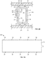
- FIG. 2A is a top view showing a group of near field communication antennas 16 after a first partial stamping by the first stamping press.
- the antennas 18a-e include tie bars 20 and carriers 22 to add stability and support to the partially stamped antennas.
- the copper sheet is cut so that a near field communication antenna biscuit is created having a group of antennas, e.g., five as shown in FIG. 2A .
- the biscuit 16 includes antennas 18a-e connected with carriers 22 and a series of tie bars 20 that extend between the antennas 18a-3 and within each respective antenna 18a-e.
- the biscuit 16 also includes a plurality of pilot holes 24, which will be discussed in greater detail.
- FIG. 2B is a top view of an individual antenna 18a from the near field communication antenna biscuit 16 showing the individual antenna 18a in greater detail.
- the antenna 18a includes an intricate shape of thin traces 26 connected to two paddles 28 or contacts.
- the traces 26 are interconnected by the series of tie bars 20 and connected to the carriers 22.
- the series of tie bars 20 and carriers 22 provide stabilization, support, and strength for the thin traces 26 of the antenna 18a so that the traces 26 can be further processed without risk of breakage.
- the two contacts 28 could be gold plated.
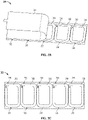
- FIG. 3A is a top view of a PSA pad 30 including a release liner 34.
- FIG. 3B is a perspective view of the PSA pad 30 of FIG. 3A with the release liner 34 partially removed.
- FIG. 3C is a perspective view of the PSA pad 30 with the release liner 34 completely removed. Removal of the release liner 34 exposes a plurality of adhesive areas 36, having the general shape of the antennas.
- the PSA pad 30 includes a release liner 34, adhesive areas 36, and a plurality of die cut holes 38.
- the PSA pad 30 of FIGS. 3A-3C includes five adhesive areas 36 to match the five antenna 18a-e.
- the adhesive areas 36 are located and shaped to match the five antenna 18a-e such that the antenna traces 26 and contacts 28 are bonded with the adhesive areas 36.
- the plurality of die cut holes 38 could be positioned along the perimeter of the PSA pad 30.
- the die cut holes 38 match with any fixture pins 42 on the fixture 32 or jig, as well as the pilot holes 24 of the antenna biscuit 16, and facilitate alignment of the PSA pad 30 on the fixture 32, and alignment of the PSA pad 30 with the antenna biscuit 16.
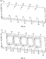
- FIG. 4 is a perspective view of a fixture 32 for receiving the PSA pad 30 and the antenna biscuit 16.
- the fixture 32 includes a body 40 and a plurality of pins 42 for alignment of the PSA pad 30 and the antenna biscuit 16.
- FIG. 5 is a perspective view of the PSA pad 30 on the fixture 32 of FIG. 4 .
- the PSA pad 30 is placed over the fixture 32 so that the plurality of pins 42 are inserted into the die cut holes 38 of the PSA pad 30.
- the release liner 34 of the PSA pad 30 is removed prior to placing the PSA pad 30 onto the fixture 32.
- FIG. 6 is a perspective view of the group of antennas 16 of FIG. 1 on the fixture 32 having a PSA pad 30 already placed thereon.
- the plurality of fixture pins 42 extend through the die cut holes 38 of the PSA pad 30 and facilitate alignment of the PSA pad 30 and the near field communication antenna biscuit 16.
- the near field communication antenna biscuit 16 is placed onto the fixture 32 so that the fixture pins 42 extend through the pilot holes 24.
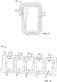
- FIG. 7 is a top view showing the near field communication antenna biscuit 16 and the PSA pad 30 on the fixture 32. As can be seen, the traces 26 of each antenna 18a-e overlap an adhesive portion 36 of the PSA pad 30.
- the previously removed release liner 34 is then placed on top of the near field communication antenna biscuit 16 as shown in FIG. 8 . Placing the release liner 34 over the near field communication antenna biscuit 16 protects the PSA pad 30 during additional stamping processes.
- the fixture 32, PSA pad 30 and antenna biscuit 16 are transferred to a fourth station 44 for bonding the antenna biscuit 16 with the PSA pad 30.
- the fourth station 44 includes rollers that provide pressure for activating the PSA 30 and bonding the antenna biscuit 16 with the PSA pad 30.
- the antenna biscuit 16, now with a PSA layer 30, is advanced to a fifth station 46 that includes a second precision high-speed stamping press for performing a second antenna stamping.
- the second stamping press performs a second stamping operation on the antenna biscuit 16 wherein the tie bars 20 are stamped and removed from each antenna 18a-e.
- the second stamping press stamps through the foil that makes up the tie bars 20, the PSA bonded to the tie bars 20, and the release liner 34.
- FIG. 9 is a top view of the antenna biscuit 16, PSA pad 30, and release liner 34 after the secondary stamping.
- the antenna biscuit 16 and PSA pad 30 cannot be seen because they are covered by the release liner 34.
- the second stamping process can also stamp a plurality of guide holes 48 for future ferrite shield application, which will be discussed in greater detail.
- FIG. 10 is a perspective view showing the release liner 34 removed from the antenna biscuit 16.
- the PSA pad 30 may be cut so that each individual antenna 18a-e is separated from one another.
- FIG. 11 is a top view of an individual antenna 18a after the second stamping and separated from the other individual antennas 18b-e.
- the completed antenna 18a no longer includes a tie bar 20 connecting the traces 26 or the contacts 28.
- the completed antennas 18a-e can then be sent to a sixth station 50 where they are packaged for distribution.
- FIG. 12 is a view of a ferrite shield 54 assembly sheet that may be used.
- the ferrite shield assembly sheet 54 includes a liner 56, a series of ferrite shields 58, and a plurality of pilot holes 60.
- the ferrite shield assembly sheet 54 is generally sized, dimensioned, and arranged so that each individual ferrite shield 58 generally overlaps a respective antenna 18a-e of the antenna biscuit 16.
- FIG. 13 is a perspective view of the antennas 18a-e and PSA pad 30 sub-assembly placed on a fixture, with the antennas 18a-e facing upward and the PSA pad 30 abutting the fixture 62.
- the fixture 62 includes a body 64 and a plurality of guide pins 66 that are aligned with and inserted into the guide holes 48 the PSA pad 30.
- the ferrite shield assembly sheet 54 of FIG. 12 is placed on to the fixture 62 such that the guide pins 66 of the fixture 62 are aligned with and inserted into the pilot holes 60 of the ferrite shield assembly sheet 54.
- the ferrite shield assembly sheet 54 is oriented such that the series of ferrite shields 58 are facing the copper antennas 18a-e.
- the ferrite shields 58 overlap the antennas 18a-e, such that there is one ferrite shield 58 for each individual antenna 18a-e.
- the ferrite shields 58 are then bonded to the respective antenna 18a-e by means that are known in the art, for example, a vacuum adhesive.
- the ferrite shield liner 56 can be removed, leaving a series of five individual antenna 18a-e each having a ferrite shield 58 bonded thereto, as shown in FIG. 15 .
- the antennas 18a-e, held together as a group by the PSA pad 30, can be cut into individual antenna 18a-e and the PSA pad 30 can be removed.
- FIGS. 16-17 show an antenna 18a having a ferrite shield 58.
- FIGS. 18-20 show an alternative embodiment in which a pallet 70 is used in place of the fixture 32.
- the pallet 70 includes a body 72, a handle 74 extending from the body 72, a plurality of pilot holes 76, a plurality of guide pins 78, and a plurality of removed sections 80.
- the plurality of pilot holes 76 are positioned to match guide pins of a stamping machine so that the pallet 70 is properly aligned when engaged with the machine.
- the plurality of guide pins 78 facilitate positioning a PSA pad 30, antenna biscuit 16, and ferrite shield assembly sheet 54 during manufacturing.
- the guide pins 78 ensure that the PSA pad 30 and antenna biscuit 16 are located such that the tie bars 20, carriers 22, and portions that need to be cut by pressing are positioned over the removed sections 80.
- the removed sections 80 allow a die to be pressed through the PSA pad 30 and the antenna biscuit 16, thus facilitating removal of the tie bars 20 and carriers 22.
- FIGS. 21-25 shown another method for applying a ferrite shield layer.
- FIG. 21 is a top view of a ferrite shield assembly sheet 82 placed on a first fixture or pallet 84.
- the ferrite shield assembly 82 includes a liner 86 and a plurality of ferrite shields 88.
- the ferrite shield assembly 82 is placed on the first fixture 84 such that the ferrite shields 88 are face down on the first fixture 84, e.g., adjacent the first fixture 84, and the liner 86 is face up.
- the first fixture 84 can include a vacuum or magnets that hold the ferrite shields 88 in place. Accordingly, the liner 86 can be removed from the ferrite shields 88, and the ferrite shields 88 will be retained in place by the fixture 84.
- FIG. 22A is a top view of the ferrite shields 88 on the first fixture 84.
- FIG. 22B is a top view of the plurality of antennas 18a-e on a second fixture or pallet 90.
- FIG. 22C is a top view of a plurality of adhesive cards 92.
- Each of the plurality of adhesive cards 92 includes a bottom release liner (not shown), a top liner 94, an adhesive area 96, an two alignment holes 98.
- the bottom release liner is a continuous liner that spans one or more of the adhesive cards such as the five adhesive cards 92 shown, and is removed during assembly to expose the adhesive areas 96.
- the top liner 94 is cut into a square/rectangle that extends beyond the edges of the adhesive area 96.
- the two alignment holes 98 facilitate alignment of the adhesive cards 92 with a pick-up pad.
- FIG. 23 is a top view of an adhesive card 92, an antenna 18a, and a ferrite shield 88, showing the order that they are assembled. As shown in FIG. 23 , the adhesive card 92 is first applied to the antenna 18a, and then the ferrite shield 88 is applied over the antenna 18a and onto the adhesive card 92. This application process is discussed in greater detail in connection with FIG. 25 .
- FIG. 24 is an exploded side view of a completed antenna 100 including a ferrite shield 88. The completed antenna 100 includes a plurality of layers that include, from top to bottom, the top liner 94, the adhesive area 96, the antenna 18a, and the ferrite shield 88.
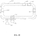
- FIG. 25 is a plan view of a sample manufacturing process for applying the ferrite shield 88.
- the antenna biscuit with PSA layer 30 can be transferred to a loading station 102, where it is loaded onto a conveyor belt or track 104.
- the antenna biscuit is transferred to a second or complete stamping station 106 where the tie-bars are removed and the antennas are singulated by a second stamping process, which is in accordance with the fifth station 46 of FIG. 1 , described above.
- the individual antennas are delivered by the conveyor 104 to a pallet loading station 108 where the antennas are placed on a pallet or plate.
- the pallet could be configured like the pallet 70 shown in FIGS. 18-20 .
- the pallet can hold any number of antennas, such as five antennas, for example.
- the pallet with antennas is then conveyed to an assembly station 110.
- the assembly station 110 could include a robotic device 112, which could have 3-axis movement, an adhesive applicator 114, and a robotic cylinder 116.
- the assembly station 110 receives the antennas and attaches the ferrite shields 88.
- the adhesive applicator 114 removes the bottom liner of the adhesive cards 92, rolls the removed bottom liner onto a scrap roller, and places each adhesive card 92 into a tray of the robotic cylinder 116.
- the robotic cylinder 116 transfers the adhesive cards 92 to the robotic device 112.
- the robot device 112 could be a robotic pick-up pad that could be a vacuum pad attached to the end of an arm of the robotic device 112 to pick up the adhesive cards 92.
- the robotic device 112 includes pilot pins that engage the alignment holes 98 of the adhesive cards 92 and locate/align the adhesive cards 92. Once the adhesive cards 92 are ready for transferring, the robotic device 112 moves the adhesive cards 92 into alignment over the antennas, which are transferred by the pallet 70. The robot 112 then stamps the adhesive cards 92 onto the antennas, such that the adhesive areas 96 engage the antennas, and picks the antennas up. Next, the robotic device 112 moves the adhesive card 92 and antenna sub-assembly over the first fixture 84 containing the ferrite shields 88, and stamps down on the ferrite shields 88 to bond the ferrite shields 88 to the antennas and the adhesive cards 92. The antennas, including adhesive cards 92 and ferrite shields 88, are then transferred along the conveyor belt to a pick-and-pack station 118 where the antennas are removed from the conveyor 104, scrap is removed, and the antennas are packaged.
Landscapes
- Engineering & Computer Science (AREA)
- Computer Hardware Design (AREA)
- Microelectronics & Electronic Packaging (AREA)
- Physics & Mathematics (AREA)
- General Physics & Mathematics (AREA)
- Theoretical Computer Science (AREA)
- Computer Networks & Wireless Communication (AREA)
- Manufacturing & Machinery (AREA)
- Support Of Aerials (AREA)
- Details Of Aerials (AREA)
- Shielding Devices Or Components To Electric Or Magnetic Fields (AREA)
Priority Applications (3)
| Application Number | Priority Date | Filing Date | Title |
|---|---|---|---|
| EP24150890.2A EP4366082A1 (en) | 2013-03-15 | 2014-03-12 | Stamped antenna and method of manufacturing |
| DK22186931.6T DK4131642T3 (da) | 2013-03-15 | 2014-03-12 | Udstanset antenne og fremstillingsfremgangsmåde |
| EP22186931.6A EP4131642B1 (en) | 2013-03-15 | 2014-03-12 | Stamped antenna and method of manufacturing |
Applications Claiming Priority (2)
| Application Number | Priority Date | Filing Date | Title |
|---|---|---|---|
| US13/833,888 US9252478B2 (en) | 2013-03-15 | 2013-03-15 | Method of manufacturing stamped antenna |
| PCT/US2014/023861 WO2014150641A1 (en) | 2013-03-15 | 2014-03-12 | Stamped antenna and method of manufacturing |
Related Child Applications (3)
| Application Number | Title | Priority Date | Filing Date |
|---|---|---|---|
| EP22186931.6A Division-Into EP4131642B1 (en) | 2013-03-15 | 2014-03-12 | Stamped antenna and method of manufacturing |
| EP22186931.6A Division EP4131642B1 (en) | 2013-03-15 | 2014-03-12 | Stamped antenna and method of manufacturing |
| EP24150890.2A Division EP4366082A1 (en) | 2013-03-15 | 2014-03-12 | Stamped antenna and method of manufacturing |
Publications (3)
| Publication Number | Publication Date |
|---|---|
| EP2973852A1 EP2973852A1 (en) | 2016-01-20 |
| EP2973852A4 EP2973852A4 (en) | 2016-11-16 |
| EP2973852B1 true EP2973852B1 (en) | 2022-10-26 |
Family
ID=51520628
Family Applications (3)
| Application Number | Title | Priority Date | Filing Date |
|---|---|---|---|
| EP24150890.2A Pending EP4366082A1 (en) | 2013-03-15 | 2014-03-12 | Stamped antenna and method of manufacturing |
| EP22186931.6A Active EP4131642B1 (en) | 2013-03-15 | 2014-03-12 | Stamped antenna and method of manufacturing |
| EP14769760.1A Active EP2973852B1 (en) | 2013-03-15 | 2014-03-12 | Method of manufacturing a stamped antenna |
Family Applications Before (2)
| Application Number | Title | Priority Date | Filing Date |
|---|---|---|---|
| EP24150890.2A Pending EP4366082A1 (en) | 2013-03-15 | 2014-03-12 | Stamped antenna and method of manufacturing |
| EP22186931.6A Active EP4131642B1 (en) | 2013-03-15 | 2014-03-12 | Stamped antenna and method of manufacturing |
Country Status (12)
| Country | Link |
|---|---|
| US (4) | US9252478B2 (enExample) |
| EP (3) | EP4366082A1 (enExample) |
| JP (1) | JP6453842B2 (enExample) |
| KR (1) | KR102136915B1 (enExample) |
| CN (1) | CN105229854B (enExample) |
| CA (1) | CA2906430C (enExample) |
| DK (2) | DK2973852T3 (enExample) |
| ES (2) | ES2981169T3 (enExample) |
| FI (1) | FI4131642T3 (enExample) |
| PL (2) | PL2973852T3 (enExample) |
| PT (2) | PT2973852T (enExample) |
| WO (1) | WO2014150641A1 (enExample) |
Families Citing this family (3)
| Publication number | Priority date | Publication date | Assignee | Title |
|---|---|---|---|---|
| US9252478B2 (en) * | 2013-03-15 | 2016-02-02 | A.K. Stamping Company, Inc. | Method of manufacturing stamped antenna |
| EP3365942B1 (en) | 2016-10-18 | 2024-02-28 | Telefonaktiebolaget LM Ericsson (PUBL) | System comprising a surface integrated antenna array and a test fixture assembly. |
| US11123871B2 (en) | 2018-04-26 | 2021-09-21 | Walmart Apollo, Llc | Systems and methods autonomously performing instructed operations using a robotic device |
Family Cites Families (23)
| Publication number | Priority date | Publication date | Assignee | Title |
|---|---|---|---|---|
| US5199157A (en) * | 1992-01-21 | 1993-04-06 | Adaptive Technology, Inc. | Continuous manufacture of formed, plated component parts having selected alternate configurations |
| US6250192B1 (en) | 1996-11-12 | 2001-06-26 | Micron Technology, Inc. | Method for sawing wafers employing multiple indexing techniques for multiple die dimensions |
| JP3361489B2 (ja) * | 1998-10-02 | 2003-01-07 | 新光電気工業株式会社 | Icカードの製造方法 |
| JP2000072819A (ja) | 1999-08-12 | 2000-03-07 | Mitsubishi Chemicals Corp | エチレン系重合体 |
| US6326920B1 (en) | 2000-03-09 | 2001-12-04 | Avaya Technology Corp. | Sheet-metal antenna |
| US7159298B2 (en) * | 2001-03-15 | 2007-01-09 | Daniel Lieberman | Method for the formation of RF antennas by demetallizing |
| JP2004342755A (ja) * | 2003-05-14 | 2004-12-02 | Shinko Electric Ind Co Ltd | 平面コイルの製造方法 |
| WO2005089143A2 (en) * | 2004-03-12 | 2005-09-29 | A K Stamping Co. Inc. | Manufacture of rfid tags and intermediate products therefor |
| US7229018B2 (en) | 2004-08-03 | 2007-06-12 | Kurz Arthur A | Manufacture of RFID tags and intermediate products therefor |
| US7500307B2 (en) * | 2004-09-22 | 2009-03-10 | Avery Dennison Corporation | High-speed RFID circuit placement method |
| US7749350B2 (en) * | 2005-04-27 | 2010-07-06 | Avery Dennison Retail Information Services | Webs and methods of making same |
| US20070014462A1 (en) * | 2005-07-13 | 2007-01-18 | Mikael Rousson | Constrained surface evolutions for prostate and bladder segmentation in CT images |
| US7555826B2 (en) | 2005-12-22 | 2009-07-07 | Avery Dennison Corporation | Method of manufacturing RFID devices |
| US7705785B2 (en) * | 2005-12-23 | 2010-04-27 | Advanced Connectek Inc. | Antenna patch arrays integrally formed with a network thereof |
| US7952322B2 (en) | 2006-01-31 | 2011-05-31 | Mojo Mobility, Inc. | Inductive power source and charging system |
| JP4929813B2 (ja) * | 2006-04-21 | 2012-05-09 | 大日本印刷株式会社 | 非接触式データキャリアインレット及び非接触式データキャリア |
| US7637000B2 (en) | 2006-10-25 | 2009-12-29 | Continental Automotive Systems Us, Inc. | Plated antenna from stamped metal coil |
| JP4851982B2 (ja) * | 2007-04-11 | 2012-01-11 | 日精樹脂工業株式会社 | カード形部品の製造方法及び装置 |
| TWI370580B (en) | 2007-12-27 | 2012-08-11 | Wistron Neweb Corp | Patch antenna and method of making same |
| CA2751757A1 (en) | 2009-02-03 | 2010-08-12 | Miller Dowel Company | Beveled block pallet |
| US20100318440A1 (en) | 2010-03-18 | 2010-12-16 | Coveley Michael Ej | Cashierless, Hygienic, Automated, Computerized, Programmed Shopping Store, Storeroom And Supply Pipeline With Administration Cataloguing To Eliminate Retail Fraud; With Innovative Components For Use Therein |
| JPWO2011155401A1 (ja) * | 2010-06-07 | 2013-08-01 | 株式会社フジクラ | フィルムアンテナ及びその製造方法 |
| US9252478B2 (en) * | 2013-03-15 | 2016-02-02 | A.K. Stamping Company, Inc. | Method of manufacturing stamped antenna |
-
2013
- 2013-03-15 US US13/833,888 patent/US9252478B2/en active Active
-
2014
- 2014-03-12 EP EP24150890.2A patent/EP4366082A1/en active Pending
- 2014-03-12 ES ES22186931T patent/ES2981169T3/es active Active
- 2014-03-12 ES ES14769760T patent/ES2931315T3/es active Active
- 2014-03-12 CN CN201480027288.XA patent/CN105229854B/zh active Active
- 2014-03-12 JP JP2016501366A patent/JP6453842B2/ja active Active
- 2014-03-12 PL PL14769760.1T patent/PL2973852T3/pl unknown
- 2014-03-12 EP EP22186931.6A patent/EP4131642B1/en active Active
- 2014-03-12 KR KR1020157029106A patent/KR102136915B1/ko active Active
- 2014-03-12 PT PT147697601T patent/PT2973852T/pt unknown
- 2014-03-12 EP EP14769760.1A patent/EP2973852B1/en active Active
- 2014-03-12 PL PL22186931.6T patent/PL4131642T3/pl unknown
- 2014-03-12 DK DK14769760.1T patent/DK2973852T3/da active
- 2014-03-12 PT PT221869316T patent/PT4131642T/pt unknown
- 2014-03-12 WO PCT/US2014/023861 patent/WO2014150641A1/en not_active Ceased
- 2014-03-12 FI FIEP22186931.6T patent/FI4131642T3/fi active
- 2014-03-12 DK DK22186931.6T patent/DK4131642T3/da active
- 2014-03-12 CA CA2906430A patent/CA2906430C/en active Active
-
2016
- 2016-02-01 US US15/012,051 patent/US10096895B2/en active Active
- 2016-02-01 US US15/012,037 patent/US10186766B2/en active Active
-
2018
- 2018-10-09 US US16/155,339 patent/US10910704B2/en active Active
Also Published As
| Publication number | Publication date |
|---|---|
| KR102136915B1 (ko) | 2020-07-23 |
| PL4131642T3 (pl) | 2024-07-29 |
| JP2016515363A (ja) | 2016-05-26 |
| WO2014150641A1 (en) | 2014-09-25 |
| CN105229854B (zh) | 2018-06-01 |
| EP4131642B1 (en) | 2024-02-28 |
| US10910704B2 (en) | 2021-02-02 |
| DK2973852T3 (da) | 2022-11-14 |
| FI4131642T3 (fi) | 2024-05-29 |
| CN105229854A (zh) | 2016-01-06 |
| HK1218464A1 (en) | 2017-02-17 |
| CA2906430A1 (en) | 2014-09-25 |
| PT4131642T (pt) | 2024-05-23 |
| US20140259638A1 (en) | 2014-09-18 |
| EP4366082A1 (en) | 2024-05-08 |
| US10186766B2 (en) | 2019-01-22 |
| ES2931315T3 (es) | 2022-12-28 |
| EP2973852A4 (en) | 2016-11-16 |
| ES2981169T3 (es) | 2024-10-07 |
| US20160149296A1 (en) | 2016-05-26 |
| EP2973852A1 (en) | 2016-01-20 |
| US20160149295A1 (en) | 2016-05-26 |
| CA2906430C (en) | 2022-04-26 |
| US9252478B2 (en) | 2016-02-02 |
| EP4131642A1 (en) | 2023-02-08 |
| US10096895B2 (en) | 2018-10-09 |
| PT2973852T (pt) | 2022-11-25 |
| DK4131642T3 (da) | 2024-05-27 |
| KR20150132378A (ko) | 2015-11-25 |
| JP6453842B2 (ja) | 2019-01-16 |
| PL2973852T3 (pl) | 2023-01-02 |
| US20190044225A1 (en) | 2019-02-07 |
Similar Documents
| Publication | Publication Date | Title |
|---|---|---|
| US20220164621A1 (en) | Method of assembly of articles and intermediate created thereby | |
| US20080124842A1 (en) | Method and apparatus for linear die transfer | |
| US10910704B2 (en) | Systems for manufacturing an antenna | |
| EP1746636A1 (en) | IC chip mounting method | |
| US10049319B2 (en) | Method of assembly using moving substrates, including creating RFID inlays | |
| WO2018142869A1 (ja) | Rfidタグの製造方法、rfidタグの製造装置、及び転写シートの製造方法 | |
| HK1218464B (en) | Method of manufacturing a stamped antenna | |
| JP6418298B2 (ja) | キャリアテープ及びその製造方法、並びにrfidタグの製造方法 | |
| JP4809648B2 (ja) | 電子装置の製造方法 | |
| JP6206626B1 (ja) | キャリアテープ及びその製造方法、並びにrfidタグの製造方法 | |
| CN210348526U (zh) | 一种四孔定位的复合导磁片的lm5射频标签模块 | |
| EP2573717B1 (en) | A method of incorporating an element in a data carrier |
Legal Events
| Date | Code | Title | Description |
|---|---|---|---|
| PUAI | Public reference made under article 153(3) epc to a published international application that has entered the european phase |
Free format text: ORIGINAL CODE: 0009012 |
|
| 17P | Request for examination filed |
Effective date: 20150915 |
|
| AK | Designated contracting states |
Kind code of ref document: A1 Designated state(s): AL AT BE BG CH CY CZ DE DK EE ES FI FR GB GR HR HU IE IS IT LI LT LU LV MC MK MT NL NO PL PT RO RS SE SI SK SM TR |
|
| AX | Request for extension of the european patent |
Extension state: BA ME |
|
| DAX | Request for extension of the european patent (deleted) | ||
| A4 | Supplementary search report drawn up and despatched |
Effective date: 20161018 |
|
| RIC1 | Information provided on ipc code assigned before grant |
Ipc: H01Q 1/22 20060101ALI20161012BHEP Ipc: G06K 19/077 20060101ALI20161012BHEP Ipc: H01Q 1/38 20060101AFI20161012BHEP |
|
| REG | Reference to a national code |
Ref country code: HK Ref legal event code: DE Ref document number: 1218464 Country of ref document: HK |
|
| STAA | Information on the status of an ep patent application or granted ep patent |
Free format text: STATUS: EXAMINATION IS IN PROGRESS |
|
| 17Q | First examination report despatched |
Effective date: 20201021 |
|
| GRAP | Despatch of communication of intention to grant a patent |
Free format text: ORIGINAL CODE: EPIDOSNIGR1 |
|
| STAA | Information on the status of an ep patent application or granted ep patent |
Free format text: STATUS: GRANT OF PATENT IS INTENDED |
|
| INTG | Intention to grant announced |
Effective date: 20211202 |
|
| GRAJ | Information related to disapproval of communication of intention to grant by the applicant or resumption of examination proceedings by the epo deleted |
Free format text: ORIGINAL CODE: EPIDOSDIGR1 |
|
| STAA | Information on the status of an ep patent application or granted ep patent |
Free format text: STATUS: EXAMINATION IS IN PROGRESS |
|
| GRAP | Despatch of communication of intention to grant a patent |
Free format text: ORIGINAL CODE: EPIDOSNIGR1 |
|
| STAA | Information on the status of an ep patent application or granted ep patent |
Free format text: STATUS: GRANT OF PATENT IS INTENDED |
|
| INTC | Intention to grant announced (deleted) | ||
| INTG | Intention to grant announced |
Effective date: 20220405 |
|
| GRAS | Grant fee paid |
Free format text: ORIGINAL CODE: EPIDOSNIGR3 |
|
| RIN1 | Information on inventor provided before grant (corrected) |
Inventor name: ANDREWS, MARK Inventor name: KURZ, ARTHUR |
|
| GRAA | (expected) grant |
Free format text: ORIGINAL CODE: 0009210 |
|
| STAA | Information on the status of an ep patent application or granted ep patent |
Free format text: STATUS: THE PATENT HAS BEEN GRANTED |
|
| RAP3 | Party data changed (applicant data changed or rights of an application transferred) |
Owner name: A.K. STAMPING COMPANY, INC. |
|
| AK | Designated contracting states |
Kind code of ref document: B1 Designated state(s): AL AT BE BG CH CY CZ DE DK EE ES FI FR GB GR HR HU IE IS IT LI LT LU LV MC MK MT NL NO PL PT RO RS SE SI SK SM TR |
|
| REG | Reference to a national code |
Ref country code: GB Ref legal event code: FG4D |
|
| REG | Reference to a national code |
Ref country code: CH Ref legal event code: EP |
|
| REG | Reference to a national code |
Ref country code: DK Ref legal event code: T3 Effective date: 20221110 |
|
| REG | Reference to a national code |
Ref country code: AT Ref legal event code: REF Ref document number: 1527733 Country of ref document: AT Kind code of ref document: T Effective date: 20221115 |
|
| REG | Reference to a national code |
Ref country code: DE Ref legal event code: R096 Ref document number: 602014085331 Country of ref document: DE |
|
| REG | Reference to a national code |
Ref country code: IE Ref legal event code: FG4D |
|
| REG | Reference to a national code |
Ref country code: PT Ref legal event code: SC4A Ref document number: 2973852 Country of ref document: PT Date of ref document: 20221125 Kind code of ref document: T Free format text: AVAILABILITY OF NATIONAL TRANSLATION Effective date: 20221118 |
|
| REG | Reference to a national code |
Ref country code: SE Ref legal event code: TRGR |
|
| REG | Reference to a national code |
Ref country code: NL Ref legal event code: FP |
|
| REG | Reference to a national code |
Ref country code: ES Ref legal event code: FG2A Ref document number: 2931315 Country of ref document: ES Kind code of ref document: T3 Effective date: 20221228 |
|
| REG | Reference to a national code |
Ref country code: GR Ref legal event code: EP Ref document number: 20220402288 Country of ref document: GR Effective date: 20221212 |
|
| REG | Reference to a national code |
Ref country code: NO Ref legal event code: T2 Effective date: 20221026 |
|
| REG | Reference to a national code |
Ref country code: LT Ref legal event code: MG9D |
|
| PG25 | Lapsed in a contracting state [announced via postgrant information from national office to epo] |
Ref country code: LT Free format text: LAPSE BECAUSE OF FAILURE TO SUBMIT A TRANSLATION OF THE DESCRIPTION OR TO PAY THE FEE WITHIN THE PRESCRIBED TIME-LIMIT Effective date: 20221026 |
|
| PGFP | Annual fee paid to national office [announced via postgrant information from national office to epo] |
Ref country code: NO Payment date: 20230329 Year of fee payment: 10 Ref country code: IE Payment date: 20230327 Year of fee payment: 10 Ref country code: FR Payment date: 20230327 Year of fee payment: 10 Ref country code: FI Payment date: 20230327 Year of fee payment: 10 Ref country code: DK Payment date: 20230329 Year of fee payment: 10 Ref country code: AT Payment date: 20230221 Year of fee payment: 10 |
|
| PG25 | Lapsed in a contracting state [announced via postgrant information from national office to epo] |
Ref country code: RS Free format text: LAPSE BECAUSE OF FAILURE TO SUBMIT A TRANSLATION OF THE DESCRIPTION OR TO PAY THE FEE WITHIN THE PRESCRIBED TIME-LIMIT Effective date: 20221026 Ref country code: LV Free format text: LAPSE BECAUSE OF FAILURE TO SUBMIT A TRANSLATION OF THE DESCRIPTION OR TO PAY THE FEE WITHIN THE PRESCRIBED TIME-LIMIT Effective date: 20221026 Ref country code: IS Free format text: LAPSE BECAUSE OF FAILURE TO SUBMIT A TRANSLATION OF THE DESCRIPTION OR TO PAY THE FEE WITHIN THE PRESCRIBED TIME-LIMIT Effective date: 20230226 Ref country code: HR Free format text: LAPSE BECAUSE OF FAILURE TO SUBMIT A TRANSLATION OF THE DESCRIPTION OR TO PAY THE FEE WITHIN THE PRESCRIBED TIME-LIMIT Effective date: 20221026 |
|
| PGFP | Annual fee paid to national office [announced via postgrant information from national office to epo] |
Ref country code: TR Payment date: 20230224 Year of fee payment: 10 Ref country code: SE Payment date: 20230315 Year of fee payment: 10 Ref country code: PT Payment date: 20230222 Year of fee payment: 10 Ref country code: PL Payment date: 20230306 Year of fee payment: 10 Ref country code: IT Payment date: 20230321 Year of fee payment: 10 Ref country code: GR Payment date: 20230331 Year of fee payment: 10 Ref country code: GB Payment date: 20230327 Year of fee payment: 10 Ref country code: DE Payment date: 20230329 Year of fee payment: 10 Ref country code: BE Payment date: 20230327 Year of fee payment: 10 |
|
| PGFP | Annual fee paid to national office [announced via postgrant information from national office to epo] |
Ref country code: NL Payment date: 20230326 Year of fee payment: 10 |
|
| P01 | Opt-out of the competence of the unified patent court (upc) registered |
Effective date: 20230526 |
|
| REG | Reference to a national code |
Ref country code: DE Ref legal event code: R097 Ref document number: 602014085331 Country of ref document: DE |
|
| PG25 | Lapsed in a contracting state [announced via postgrant information from national office to epo] |
Ref country code: SM Free format text: LAPSE BECAUSE OF FAILURE TO SUBMIT A TRANSLATION OF THE DESCRIPTION OR TO PAY THE FEE WITHIN THE PRESCRIBED TIME-LIMIT Effective date: 20221026 Ref country code: RO Free format text: LAPSE BECAUSE OF FAILURE TO SUBMIT A TRANSLATION OF THE DESCRIPTION OR TO PAY THE FEE WITHIN THE PRESCRIBED TIME-LIMIT Effective date: 20221026 Ref country code: EE Free format text: LAPSE BECAUSE OF FAILURE TO SUBMIT A TRANSLATION OF THE DESCRIPTION OR TO PAY THE FEE WITHIN THE PRESCRIBED TIME-LIMIT Effective date: 20221026 Ref country code: CZ Free format text: LAPSE BECAUSE OF FAILURE TO SUBMIT A TRANSLATION OF THE DESCRIPTION OR TO PAY THE FEE WITHIN THE PRESCRIBED TIME-LIMIT Effective date: 20221026 |
|
| PGFP | Annual fee paid to national office [announced via postgrant information from national office to epo] |
Ref country code: ES Payment date: 20230403 Year of fee payment: 10 Ref country code: CH Payment date: 20230402 Year of fee payment: 10 |
|
| PG25 | Lapsed in a contracting state [announced via postgrant information from national office to epo] |
Ref country code: SK Free format text: LAPSE BECAUSE OF FAILURE TO SUBMIT A TRANSLATION OF THE DESCRIPTION OR TO PAY THE FEE WITHIN THE PRESCRIBED TIME-LIMIT Effective date: 20221026 Ref country code: AL Free format text: LAPSE BECAUSE OF FAILURE TO SUBMIT A TRANSLATION OF THE DESCRIPTION OR TO PAY THE FEE WITHIN THE PRESCRIBED TIME-LIMIT Effective date: 20221026 |
|
| PLBE | No opposition filed within time limit |
Free format text: ORIGINAL CODE: 0009261 |
|
| STAA | Information on the status of an ep patent application or granted ep patent |
Free format text: STATUS: NO OPPOSITION FILED WITHIN TIME LIMIT |
|
| 26N | No opposition filed |
Effective date: 20230727 |
|
| PG25 | Lapsed in a contracting state [announced via postgrant information from national office to epo] |
Ref country code: MC Free format text: LAPSE BECAUSE OF FAILURE TO SUBMIT A TRANSLATION OF THE DESCRIPTION OR TO PAY THE FEE WITHIN THE PRESCRIBED TIME-LIMIT Effective date: 20221026 |
|
| PG25 | Lapsed in a contracting state [announced via postgrant information from national office to epo] |
Ref country code: SI Free format text: LAPSE BECAUSE OF FAILURE TO SUBMIT A TRANSLATION OF THE DESCRIPTION OR TO PAY THE FEE WITHIN THE PRESCRIBED TIME-LIMIT Effective date: 20221026 |
|
| REG | Reference to a national code |
Ref country code: AT Ref legal event code: UEP Ref document number: 1527733 Country of ref document: AT Kind code of ref document: T Effective date: 20221026 |
|
| PG25 | Lapsed in a contracting state [announced via postgrant information from national office to epo] |
Ref country code: LU Free format text: LAPSE BECAUSE OF NON-PAYMENT OF DUE FEES Effective date: 20230312 |
|
| REG | Reference to a national code |
Ref country code: DE Ref legal event code: R119 Ref document number: 602014085331 Country of ref document: DE |
|
| PG25 | Lapsed in a contracting state [announced via postgrant information from national office to epo] |
Ref country code: FI Free format text: LAPSE BECAUSE OF NON-PAYMENT OF DUE FEES Effective date: 20240312 |
|
| PG25 | Lapsed in a contracting state [announced via postgrant information from national office to epo] |
Ref country code: PT Free format text: LAPSE BECAUSE OF NON-PAYMENT OF DUE FEES Effective date: 20240912 |
|
| REG | Reference to a national code |
Ref country code: DK Ref legal event code: EBP Effective date: 20240331 |
|
| REG | Reference to a national code |
Ref country code: SE Ref legal event code: EUG |
|
| PG25 | Lapsed in a contracting state [announced via postgrant information from national office to epo] |
Ref country code: PT Free format text: LAPSE BECAUSE OF NON-PAYMENT OF DUE FEES Effective date: 20240912 Ref country code: FI Free format text: LAPSE BECAUSE OF NON-PAYMENT OF DUE FEES Effective date: 20240312 |
|
| REG | Reference to a national code |
Ref country code: CH Ref legal event code: PL |
|
| REG | Reference to a national code |
Ref country code: NL Ref legal event code: MM Effective date: 20240401 |
|
| PG25 | Lapsed in a contracting state [announced via postgrant information from national office to epo] |
Ref country code: BG Free format text: LAPSE BECAUSE OF FAILURE TO SUBMIT A TRANSLATION OF THE DESCRIPTION OR TO PAY THE FEE WITHIN THE PRESCRIBED TIME-LIMIT Effective date: 20221026 |
|
| REG | Reference to a national code |
Ref country code: AT Ref legal event code: MM01 Ref document number: 1527733 Country of ref document: AT Kind code of ref document: T Effective date: 20240312 |
|
| GBPC | Gb: european patent ceased through non-payment of renewal fee |
Effective date: 20240312 |
|
| PG25 | Lapsed in a contracting state [announced via postgrant information from national office to epo] |
Ref country code: BG Free format text: LAPSE BECAUSE OF FAILURE TO SUBMIT A TRANSLATION OF THE DESCRIPTION OR TO PAY THE FEE WITHIN THE PRESCRIBED TIME-LIMIT Effective date: 20221026 |
|
| PG25 | Lapsed in a contracting state [announced via postgrant information from national office to epo] |
Ref country code: NL Free format text: LAPSE BECAUSE OF NON-PAYMENT OF DUE FEES Effective date: 20240401 |
|
| REG | Reference to a national code |
Ref country code: BE Ref legal event code: MM Effective date: 20240331 |
|
| PG25 | Lapsed in a contracting state [announced via postgrant information from national office to epo] |
Ref country code: NL Free format text: LAPSE BECAUSE OF NON-PAYMENT OF DUE FEES Effective date: 20240401 |
|
| PG25 | Lapsed in a contracting state [announced via postgrant information from national office to epo] |
Ref country code: DE Free format text: LAPSE BECAUSE OF NON-PAYMENT OF DUE FEES Effective date: 20241001 |
|
| PG25 | Lapsed in a contracting state [announced via postgrant information from national office to epo] |
Ref country code: NO Free format text: LAPSE BECAUSE OF NON-PAYMENT OF DUE FEES Effective date: 20240331 |
|
| PG25 | Lapsed in a contracting state [announced via postgrant information from national office to epo] |
Ref country code: BE Free format text: LAPSE BECAUSE OF NON-PAYMENT OF DUE FEES Effective date: 20240331 Ref country code: GR Free format text: LAPSE BECAUSE OF NON-PAYMENT OF DUE FEES Effective date: 20241004 |
|
| PG25 | Lapsed in a contracting state [announced via postgrant information from national office to epo] |
Ref country code: GB Free format text: LAPSE BECAUSE OF NON-PAYMENT OF DUE FEES Effective date: 20240312 |
|
| PG25 | Lapsed in a contracting state [announced via postgrant information from national office to epo] |
Ref country code: FR Free format text: LAPSE BECAUSE OF NON-PAYMENT OF DUE FEES Effective date: 20240331 |
|
| PG25 | Lapsed in a contracting state [announced via postgrant information from national office to epo] |
Ref country code: AT Free format text: LAPSE BECAUSE OF NON-PAYMENT OF DUE FEES Effective date: 20240312 |
|
| PG25 | Lapsed in a contracting state [announced via postgrant information from national office to epo] |
Ref country code: IE Free format text: LAPSE BECAUSE OF NON-PAYMENT OF DUE FEES Effective date: 20240312 |
|
| PG25 | Lapsed in a contracting state [announced via postgrant information from national office to epo] |
Ref country code: NO Free format text: LAPSE BECAUSE OF NON-PAYMENT OF DUE FEES Effective date: 20240331 Ref country code: IE Free format text: LAPSE BECAUSE OF NON-PAYMENT OF DUE FEES Effective date: 20240312 Ref country code: GR Free format text: LAPSE BECAUSE OF NON-PAYMENT OF DUE FEES Effective date: 20241004 Ref country code: GB Free format text: LAPSE BECAUSE OF NON-PAYMENT OF DUE FEES Effective date: 20240312 Ref country code: FR Free format text: LAPSE BECAUSE OF NON-PAYMENT OF DUE FEES Effective date: 20240331 Ref country code: DE Free format text: LAPSE BECAUSE OF NON-PAYMENT OF DUE FEES Effective date: 20241001 Ref country code: BE Free format text: LAPSE BECAUSE OF NON-PAYMENT OF DUE FEES Effective date: 20240331 Ref country code: AT Free format text: LAPSE BECAUSE OF NON-PAYMENT OF DUE FEES Effective date: 20240312 Ref country code: CH Free format text: LAPSE BECAUSE OF NON-PAYMENT OF DUE FEES Effective date: 20240331 |
|
| PG25 | Lapsed in a contracting state [announced via postgrant information from national office to epo] |
Ref country code: DK Free format text: LAPSE BECAUSE OF NON-PAYMENT OF DUE FEES Effective date: 20240331 |
|
| PG25 | Lapsed in a contracting state [announced via postgrant information from national office to epo] |
Ref country code: IT Free format text: LAPSE BECAUSE OF NON-PAYMENT OF DUE FEES Effective date: 20240312 |
|
| REG | Reference to a national code |
Ref country code: ES Ref legal event code: FD2A Effective date: 20250506 |
|
| PG25 | Lapsed in a contracting state [announced via postgrant information from national office to epo] |
Ref country code: ES Free format text: LAPSE BECAUSE OF NON-PAYMENT OF DUE FEES Effective date: 20240313 |
|
| PG25 | Lapsed in a contracting state [announced via postgrant information from national office to epo] |
Ref country code: CY Free format text: LAPSE BECAUSE OF FAILURE TO SUBMIT A TRANSLATION OF THE DESCRIPTION OR TO PAY THE FEE WITHIN THE PRESCRIBED TIME-LIMIT; INVALID AB INITIO Effective date: 20140312 |
|
| PG25 | Lapsed in a contracting state [announced via postgrant information from national office to epo] |
Ref country code: HU Free format text: LAPSE BECAUSE OF FAILURE TO SUBMIT A TRANSLATION OF THE DESCRIPTION OR TO PAY THE FEE WITHIN THE PRESCRIBED TIME-LIMIT; INVALID AB INITIO Effective date: 20140312 |
|
| PG25 | Lapsed in a contracting state [announced via postgrant information from national office to epo] |
Ref country code: SE Free format text: LAPSE BECAUSE OF NON-PAYMENT OF DUE FEES Effective date: 20240313 |
|
| PG25 | Lapsed in a contracting state [announced via postgrant information from national office to epo] |
Ref country code: PL Free format text: LAPSE BECAUSE OF NON-PAYMENT OF DUE FEES Effective date: 20240312 |