EP2972070B1 - Method and system for real-time in-process measurement of coating thickness - Google Patents
Method and system for real-time in-process measurement of coating thickness Download PDFInfo
- Publication number
- EP2972070B1 EP2972070B1 EP14719985.5A EP14719985A EP2972070B1 EP 2972070 B1 EP2972070 B1 EP 2972070B1 EP 14719985 A EP14719985 A EP 14719985A EP 2972070 B1 EP2972070 B1 EP 2972070B1
- Authority
- EP
- European Patent Office
- Prior art keywords
- light
- processor
- wave data
- coating
- light waves
- Prior art date
- Legal status (The legal status is an assumption and is not a legal conclusion. Google has not performed a legal analysis and makes no representation as to the accuracy of the status listed.)
- Active
Links
Images

Classifications
-
- G—PHYSICS
- G01—MEASURING; TESTING
- G01B—MEASURING LENGTH, THICKNESS OR SIMILAR LINEAR DIMENSIONS; MEASURING ANGLES; MEASURING AREAS; MEASURING IRREGULARITIES OF SURFACES OR CONTOURS
- G01B11/00—Measuring arrangements characterised by the use of optical techniques
- G01B11/02—Measuring arrangements characterised by the use of optical techniques for measuring length, width or thickness
- G01B11/06—Measuring arrangements characterised by the use of optical techniques for measuring length, width or thickness for measuring thickness ; e.g. of sheet material
- G01B11/0616—Measuring arrangements characterised by the use of optical techniques for measuring length, width or thickness for measuring thickness ; e.g. of sheet material of coating
- G01B11/0641—Measuring arrangements characterised by the use of optical techniques for measuring length, width or thickness for measuring thickness ; e.g. of sheet material of coating with measurement of polarization
- G01B11/065—Measuring arrangements characterised by the use of optical techniques for measuring length, width or thickness for measuring thickness ; e.g. of sheet material of coating with measurement of polarization using one or more discrete wavelengths
-
- G—PHYSICS
- G01—MEASURING; TESTING
- G01B—MEASURING LENGTH, THICKNESS OR SIMILAR LINEAR DIMENSIONS; MEASURING ANGLES; MEASURING AREAS; MEASURING IRREGULARITIES OF SURFACES OR CONTOURS
- G01B11/00—Measuring arrangements characterised by the use of optical techniques
- G01B11/02—Measuring arrangements characterised by the use of optical techniques for measuring length, width or thickness
- G01B11/06—Measuring arrangements characterised by the use of optical techniques for measuring length, width or thickness for measuring thickness ; e.g. of sheet material
- G01B11/0616—Measuring arrangements characterised by the use of optical techniques for measuring length, width or thickness for measuring thickness ; e.g. of sheet material of coating
- G01B11/0625—Measuring arrangements characterised by the use of optical techniques for measuring length, width or thickness for measuring thickness ; e.g. of sheet material of coating with measurement of absorption or reflection
- G01B11/0633—Measuring arrangements characterised by the use of optical techniques for measuring length, width or thickness for measuring thickness ; e.g. of sheet material of coating with measurement of absorption or reflection using one or more discrete wavelengths
-
- G—PHYSICS
- G01—MEASURING; TESTING
- G01B—MEASURING LENGTH, THICKNESS OR SIMILAR LINEAR DIMENSIONS; MEASURING ANGLES; MEASURING AREAS; MEASURING IRREGULARITIES OF SURFACES OR CONTOURS
- G01B11/00—Measuring arrangements characterised by the use of optical techniques
- G01B11/02—Measuring arrangements characterised by the use of optical techniques for measuring length, width or thickness
- G01B11/06—Measuring arrangements characterised by the use of optical techniques for measuring length, width or thickness for measuring thickness ; e.g. of sheet material
- G01B11/0616—Measuring arrangements characterised by the use of optical techniques for measuring length, width or thickness for measuring thickness ; e.g. of sheet material of coating
- G01B11/0641—Measuring arrangements characterised by the use of optical techniques for measuring length, width or thickness for measuring thickness ; e.g. of sheet material of coating with measurement of polarization
Definitions
- the present disclosure generally relates to methods and systems for measuring the thickness of coatings or thin films on various substrates.
- Embodiments include methods and systems for real-time in-process measurement of coating thickness, and more particularly methods and systems for real-time in-process measurement of a coating thickness on a moving substrate or a coated product.
- the measurement of thin films and coatings is appreciated in manufacturing settings. For example, regulating the application of a thin film or coating to a product within a preferred thickness range allows manufacturers to ensure that a film or coating is applied with sufficient thickness to prevent manufacturing defects while also avoiding wasteful application of film or coating in excess of a required thickness, thereby minimizing materials costs.
- measurement of thin layers of lubricious coatings on metals allows manufacturers to ensure that sufficient coating is applied to prevent substantial damage to expensive manufacturing and processing equipment.
- modeling-based reflectometry techniques for measuring film or coating thicknesses of less than 0.2 microns have typically focused on measurement of coatings and films on semiconductor substrates.
- applications of coatings or films in the semiconductor manufacturing process are performed on static (non-moving) substrates.
- a significant limitation of the currently known modeling-based reflectometry techniques capable of measuring coatings of less than 0.2 microns is that they require a static substrate on which to perform measurements of coatings or materials deposited thereon.
- the present disclosure is directed to methods and systems for real-time in-process measurement of thin films or coatings, including films or coatings of less than 0.2 microns, on a moving substrate, and therefore overcomes the limitations of known methods and systems.
- EP 0 300 508 A2 discloses that circularly polarized light incident on a film surface (9) is converted into three light beams by optical flats (13a, 13b, 13c, 13d) to obtain electrical signals (I1-I3) corresponding to the intensities of the respective light beams. Two ellipsometric parameters ⁇ and ⁇ are calculated from these three electrical signals (I1-I3).
- the disclosed film thickness-measuring apparatus is said to be suitable for measuring an object moving at high speed or a stationary object.
- the present disclosure generally relates to a method according to claim 1 and to a system according to claim 8.
- Embodiments according to this disclosure provide methods and systems for inline real-time measurement of thin film or coating thickness, and more particularly to methods and systems for inline real-time measurement of thin film or coating thicknesses, including films or coatings of less than 0.2 microns, on a moving substrate.
- a manufacturer employs the systems and methods of the present invention to measure the thickness of a lubricious coating applied to thin metal sheeting to ensure a sufficient layer of lubricious coating is present on the thin metal sheeting-used by the manufacturer to create its products-to prevent damage to expensive manufacturing equipment that processes the metal sheeting.
- the manufacturer incorporates a broadband light source that directs light waves through polarizers and wave plates onto the surface of the thin metal sheeting containing the lubricious coating as it is moving through the equipment.
- the manufacturer further incorporates detectors that capture reflected light that passes through rotating analyzers.
- a computer controlling the manufacturing process is in communication with the light sources and the detectors and is programmed to configure the light sources to generate light within a particular spectrum range based on the particular metal and the particular lubricious coating being measured.
- the computer is further programmed to receive light wave data from the detectors.
- the computer quantifies the phase shift and polarization state changes of the reflected light, compared to the light waves generated by the light source, and then uses that information to evaluate and validate thickness of the lubricious coating at various locations on the metal sheeting as it is moving through the equipment.
- rotating analyzers and detectors are coupled to an adjustment mechanism in communication with the computer.
- the computer operates to detect flutters, vibrations, or other disturbances in the movement of the metal sheeting and automatically adjusts the positions of the analyzers and detectors to ensure accuracy of the thickness measurements.
- a preferred thickness range, warning thickness level and a critical thickness threshold are defined and programmed into the computer. If the measured thickness of the lubricious coating is well within the preferred thickness range, the computer allows the manufacturing process to continue. If the computer detects that the lubricious coating is outside of the preferred thickness range, the computer provides feedback to the system controlling the application of the lubricious coating. In response, that system adjusts the application of the lubricious coating to bring it back within the preferred thickness range. In the event that the coating thickness reaches the warning thickness level, the computer alerts the equipment operators of a potential malfunction in the lubricious coating application system. The operators may then choose whether to shut down the manufacturing process to investigate or to continue the process.
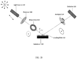
- FIG. 1A is a block diagram of a system for measuring thin film/coating thickness according to one embodiment of the present disclosure.
- FIG. 1A illustrates a configuration comprising components of system 100 according to one embodiment of the present disclosure.
- System 100 may comprise one of a variety of form factors.
- system 100 may be a self-contained system comprising a single housing.
- the system 100 may comprise a portable housing.
- the system 100 may be integrated directly into manufacturing or testing equipment.
- system 100 may comprise a number of components in separate physical locations, but coupled through wired and/or wireless communications and/or networking well known to those having ordinary skill in the art.
- Embodiments of the present disclosure can be implemented in combination with, or may comprise combinations of: digital electronic circuitry, computer hardware, firmware, software, light sources, optical equipment, and/or optical sensors.
- the system 100 shown in FIG. 1 comprises a processor 102.
- the processor 102 receives input signals and generates signals for communication, display, and processing sensor readings to measure thicknesses of thin films/coatings.
- the processor 102 includes or is in communication with one or more computer-readable media, such as memory 104, which may comprise random access memory (RAM).
- RAM random access memory
- the processor 102 executes computer-executable program instructions stored in memory 104, such as executing one or more computer programs for providing a user interface and/or processing sensor readings to measure thicknesses of thin films/coatings.
- Processor 102 may comprise a microprocessor, a digital signal processor (DSP), an application-specific integrated circuit (ASIC), one or more field programmable gate arrays (FPGAs), or state machines.
- the processor may further comprise a programmable electronic device such as a PLC, a programmable interrupt controller (PIC), a programmable logic device (PLD), a programmable read-only memory (PROM), an electronically programmable read-only memory (EPROM or EEPROM), or other similar devices.
- PLC programmable interrupt controller
- PLD programmable logic device
- PROM programmable read-only memory
- EPROM or EEPROM electronically programmable read-only memory
- Memory 104 comprises a computer-readable media that may store instructions, which, when executed by the processor 102, cause it to perform various steps, such as those described herein.
- Embodiments of computer-readable media may comprise, but are not limited to, an electronic, optical, magnetic, or other storage or transmission device capable of providing the processor 102 with computer-readable instructions.
- Other examples of media comprise, but are not limited to, a floppy disk, CD-ROM, magnetic disk, memory chip, ROM, RAM, ASIC, configured processor, all optical media, all magnetic tape or other magnetic media, or any other medium from which a computer processor can read.
- various other devices may include computer-readable media, such as a router, private or public network, or other transmission device.
- the processor 102, and the processing, described may be in one or more structures, and may be dispersed through one or more structures.
- the system 100 also comprises one or more user input devices 108 in communication with the processor 102.
- a user input device 108 may comprise a keyboard, mouse, trackball, touchscreen, touchpad, voice recognition system or any other input device known to one having ordinary skill in the art.
- the system 100 also comprises a display 106.
- Display 106 is in communication with processor 102 and is configured to display output from the processor 102 to the user.
- display 106 is a standard computer monitor such as an LCD display or a cathode ray tube (CRT).
- system 100 may comprise a touch-screen LCD that operates both as a display 106 and a user input device 108. Various sizes of LCD displays may be used.
- the system 100 further comprises a light source 110.
- light source 110 is a broadband light source capable of generating light waves of multiple wavelengths.
- the wavelengths of the illuminated light could be in the ultraviolet (UV), visible, or near infrared (NIR) regions.
- light source 110 is capable of generating light waves having wavelengths in the UV and visible spectrum regions.
- the light source 110 comprises a xenon arc lamp.
- light source 110 is capable of generating light waves having wavelengths in the visible and NIR spectrum regions.
- the light source 110 comprises a tungsten halogen lamp.
- light source 110 is capable of generating light waves having wavelengths in the UV, visible, and NIR spectrum regions.
- the light source 110 comprises a xenon arc lamp and a tungsten halogen lamp.
- light source 110 is coupled to processor 102 to allow the processor 102 to control the output of the light source 110.
- the processor 110 may communicate with the light source 110 to turn the light source 110 on or off, or to specify the type of light waves to be provided.
- the processor communicates with the light source to specify light waves within the UV, visible, and/or NIR spectrum regions, or subsets thereof.
- the processor 102 controls the amount of light generated to ensure the light levels are not saturated.
- the light source 110 may be positioned to directly emit light towards a substrate 120, as shown in FIG. 1B .
- the light guides may be used to direct light emitted from a light source 110 located at another position, such as within a housing comprising the processor 102 and memory 104, towards a substrate 120.
- the system 100 further comprises a polarizer 118.
- Polarizer 118 is an optical device that functions to convert unpolarized light waves passing through it, such as light waves provided by light source 110, into linearly polarized light waves.
- a Glan Taylor polarizer with an extinction coefficient of 10 5 :1 is used to convert the non-polarized light beam into linearly polarized light beam.
- polarizer is positioned such that light waves provided by light source 110 pass through polarizer 118.
- the system 100 further comprises a wave plate 112.
- the wave plate 112 is a quarter-wave plate Wave plate 112 functions to alter the polarization state of light waves passing through it. For example, a quarter-wave plate converts linearly polarized light waves passing through it into circularly polarized light waves.
- the wave plate 112 is positioned to receive light waves from a light source 110 that first passes through a polarizer 118.
- the light waves passing through the wave plate 112 are incident light waves to a substrate 120 comprising a coating or film 122 on the top surface.
- the wave plate 112 is rotatable and comprises a mechanism ( e.g . an electric motor) for rotating the wave plate 112.
- processor 102 communicates with wave plate 112 to control whether and at what speed the wave plate 112 is rotating.
- the system 100 further comprises an analyzer 114.
- analyzer 114 is a rotating analyzer that receives elliptically polarized light reflected by substrate 120 and/or coating or film 122.
- the rotating analyzer 114 functions to reflect light from various angular positions.
- the analyzer 114 is the same component as the polarizer 118 except that it is used to analyze the polarization state of the light wave instead of altering the polarization state of the incident light beam.
- a rotating analyzer 114 comprises a mechanism (e.g . an electric motor) for rotating the analyzer 114.
- processor 102 communicates with the rotating analyzer 114 to control whether and at what speed the analyzer 114 is rotating.
- the system 100 further comprises a detector 116.
- Detector 116 operates to detect the reflected light generated from various angular positions of the rotating analyzer.
- the detector 116 comprises a spectrometer. In some embodiments, different detectors may be used for different wavelength ranges.
- the detector 116 may be positioned to directly receive the reflected light generated from various angular positions of the rotating analyzer 114, as shown in FIG. 1B .
- a probe connected to a light guide may be used to capture and direct the reflected light generated from various angular positions of the rotating analyzer 114 to a detector 116 located at another position, such as within a housing comprising the processor 102 and memory 104.
- the probe comprises a fiber optic probe.
- the detector 116 operates to convert captured light waves into light wave data.
- light wave data may be a voltage signal waveform that corresponds to the captured light wave.
- light wave data comprises a data structure containing information that describes the capture light waves.
- the detector 116 is in communication with the processor 102 and provides the light wave data to the processor 102.
- the processor 102 is programmed to validate and evaluate the light wave data.
- the processor 102 quantifies the phase shift and polarization state changes, compared to the light waves generated by the light source 110, and then uses that information to evaluate and validate thickness of the coating/film 122 on the substrate 120.
- the processor 102 broadly calculates the polarization state change and the phase shift of the incident light waves on the sample to that of the reflected light waves emanating from the analyzer 114.
- theoretical models are developed for the given substrate coating combination and the Levenberg-Marquardt algorithm is used to calculate the best fit to match the light wave data with a theoretical model to determine thickness.
- triangular smoothing techniques are applied to light wave data to optimize the quality of spectral response before it is evaluated.
- techniques for determining signal quality and detecting noise are used to validate light wave data corresponding to individual measurements.
- signal quality of the light wave data is determined by using predetermined coating specific spectral signatures to validate individual measurements.
- the processor 102 determines the strength and quality of the light waves based on the light wave data and dynamically adjusts the light intensity provided by light source 110.
- system 100 may comprise two or more sets of light sources 110, polarizers 118, wave plates 113, analyzers 114 and detectors 116. In one such embodiment, the system 100 may simultaneously measure the thickness of the coating/film 122 at multiple locations on substrate 120.
- a single light source 110 and/or a single detector 116 may be used in conjunction with two or more sets of polarizers 118, wave plates 113, and analyzers 114.
- an optical switch and light guides coupled thereto may be used to provide light from a single light source to multiple locations on substrate 120.
- an optical switch with light guides attached thereto and probes coupled to the light guides may be used to capture the reflected light generated from various angular positions of multiple rotating analyzers 114 and direct the capture light to a single detector 116.
- two or more of light source 110 may reside in a single housing.
- analyzer 114 and detector 116 may reside in a single housing.
- analyzer 114 and detector 116 are coupled to one or more adjustment mechanisms 124 in communication with processor 102 for adjusting the position of the analyzer 114 and detector 116 (or a probe coupled to a detector 116 through a light guide).
- polarizer 118 and analyzer 114 are coupled to one or more adjustment mechanisms 124 in communication with processor 104 for adjusting the position of the polarizer 118 and analyzer 114.
- polarizer 118, analyzer 114, and detector 116 are coupled to one or more adjustment mechanisms 124 in communication with processor 102 for adjusting the position of the polarizer 118 and analyzer 114.
- the one or more adjustment mechanisms 124 may use electric motors, linear actuators, sliding tracks, gimbal mechanisms, or any other components known to one having ordinary skill in the art.
- Contemplated substrates comprise all manner of metals (e.g . aluminum, copper, nickel, titanium, steel, tin plate and other metals employed as components of or in the fabrication of products or processing of materials), a variety of films (e.g . thin stretched films, thin coatings on PET film substrates, Polyethylene Film Substrates, etc.), glass, plastics, rubber, latex, silicon ( e.g . circuit boards, wafers), and solar cells.
- Contemplated coatings comprise all manner of lubricants, waxes, liquids ( e.g .
- coatings may be sprayed onto a substrate.
- Other coatings may be rolled onto the substrate.
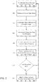
- FIG. 2 shows a flow diagram illustrating the operation of a system according to one embodiment of the present disclosure.
- FIG. 2 shows steps performed by a system to perform inline real-time measurement of thin film thickness on a moving substrate.
- steps performed by a system to perform inline real-time measurement of thin film thickness on a moving substrate are provided in the context of the illustrative diagrams of embodiments of the system shown in FIGS. 1A and 1B .
- embodiments according to the present disclosure may be implemented in alternative embodiments.
- light waves are generated and directed toward a coated substrate 120.
- the processor 102 communicates with the light source 110 to generate light waves within a one or more particular spectrum ranges to be directed at a coated substrate 120.
- a user interface provided by the processor 102 and displayed on display 106 permits a system operator to identify the substrate and/or coating material and the processor 102 then determines the appropriate light waves to select based on materials information stored in memory 104.
- the processor 102 is programmed to take into account the traits of the substrate and/or coating materials specified by a system operator to select the appropriate region of the wavelength spectrum for analysis.
- the user interface permits a system operator to manually configure the wavelength range for analysis to be used for the measurement process.
- the light waves provided by the light source 110 are linearly polarized by passing through a polarizer 118.
- the linearly polarized light waves are converted to circularly polarized light waves by passing through wave plate 112.
- wave plate 112 is a rotating quarter-wave plate.
- the processor 102 communicates with the wave plate 112 to configure the speed of the rotation of the rotating wave plate 112.
- elliptically polarized light waves reflected by the film/coating 122 and/or the substrate 120 are analyzed by an analyzer 114.
- the analyzer 114 is a rotating analyzer.
- the processor 102 communicates with the analyzer 114 to configure the speed of the rotation of the rotating analyzer 114.
- the detector 116 captures light waves reflected by the by the coated substrate 120 and then further reflected from various angular positions by analyzer 114.
- the detector 116 operates to convert the captured light waves into light wave data for communication to processor 102.
- light wave data may be a voltage signal waveform that corresponds to the captured light wave.
- light wave data comprises a data structure containing information that describes the captured light waves. Once the light wave data is generated, it is communicated to the processor 102.
- the light wave data is processed by processor 102 to determine the thickness of the film/coating 122 on the surface of substrate 120.
- processor 102 quantifies the phase shift and polarization state changes, compared to the light waves provided by the light source 110, and then uses that information to evaluate and validate thickness of the coating/film 122 on the substrate 120 using techniques disclosed herein.
- the processor 102 may process the light wave data to determine other optical parameters of the film/coating 122 such as refractive index, surface roughness, and extinction coefficient.
- the system determines whether there are vibrations, fluttering, or other disturbances in the movement of a moving substrate 120 that require adjustment of system components to obtain accurate measurements. If present, disturbances such as vibrations and flutter may impact the plane of incidence and the reflection of the light waves. In another embodiment, the system determines whether the light source 110 is providing too little or too much light. In one embodiment, disturbances and/or light level defects are identified based on the light wave data detected by detector 116 during the performance of previous iterations of the presently-described method. In some embodiments, the quality of the light wave data is validated using one or more techniques disclosed herein.
- step 202 If the light wave data is validated, indicating that there are no vibrations, fluttering, or other disturbances in the movement of substrate 120 and no light level defects that require adjustment then the method proceeds to step 202 to perform another iteration of the method. However, if the validation process determines that the data is not valid, the measurement based on the light wave is discarded and the method proceeds to step 214.
- the orientation and/or position of the optics such as analyzer 114 and polarizer 118 are adjusted in real-time to accommodate for any changes in the plane of incidence.
- the orientation and/or position of the analyzer 114 and detector 116 are adjusted in real-time to accommodate for any changes in the plane of incidence.
- the orientation and/or position of polarizer 118, analyzer 114, and/or detector 116 are adjusted in real-time to accommodate for any changes in the plane of incidence.
- processor 102 communicates commands to one or more adjustment mechanisms 124 to cause adjustment of the polarizer 118, analyzer 114, and/or the detector 116 based on the detected vibrations, fluttering, or other disturbances in the movement of substrate 120.
- the processor 102 communicates with light source 110 to adjust the intensity of the light.
Landscapes
- Physics & Mathematics (AREA)
- General Physics & Mathematics (AREA)
- Length Measuring Devices By Optical Means (AREA)
Priority Applications (1)
| Application Number | Priority Date | Filing Date | Title |
|---|---|---|---|
| PL14719985T PL2972070T3 (pl) | 2013-03-15 | 2014-03-14 | Sposób i system do pomiaru podczas procesu w czasie rzeczywistym grubości powłoki |
Applications Claiming Priority (2)
| Application Number | Priority Date | Filing Date | Title |
|---|---|---|---|
| US201361792689P | 2013-03-15 | 2013-03-15 | |
| PCT/US2014/027980 WO2014143838A1 (en) | 2013-03-15 | 2014-03-14 | Method and system for real-time in-process measurement of coating thickness |
Publications (2)
| Publication Number | Publication Date |
|---|---|
| EP2972070A1 EP2972070A1 (en) | 2016-01-20 |
| EP2972070B1 true EP2972070B1 (en) | 2020-05-27 |
Family
ID=50588890
Family Applications (1)
| Application Number | Title | Priority Date | Filing Date |
|---|---|---|---|
| EP14719985.5A Active EP2972070B1 (en) | 2013-03-15 | 2014-03-14 | Method and system for real-time in-process measurement of coating thickness |
Country Status (6)
| Country | Link |
|---|---|
| US (2) | US9863758B2 (pl) |
| EP (1) | EP2972070B1 (pl) |
| CA (2) | CA3020967A1 (pl) |
| ES (1) | ES2808550T3 (pl) |
| PL (1) | PL2972070T3 (pl) |
| WO (1) | WO2014143838A1 (pl) |
Families Citing this family (4)
| Publication number | Priority date | Publication date | Assignee | Title |
|---|---|---|---|---|
| KR102436759B1 (ko) * | 2017-10-24 | 2022-08-29 | 삼성디스플레이 주식회사 | 탈착층 성막시스템, 탈착층 성막방법, 탈착층을 포함하는 표시장치의 제조시스템 및 탈착층을 포함하는 표시장치의 제조방법 |
| KR102597603B1 (ko) | 2018-12-10 | 2023-11-02 | 삼성전자주식회사 | 검사 장치 및 이를 포함하는 반도체 구조 제조 장치 |
| CN117387546B (zh) * | 2023-12-12 | 2024-02-13 | 南京麦驰钛业有限公司 | 一种钛钢层压板高压设备检测装置 |
| CN117848262B (zh) * | 2023-12-25 | 2025-05-06 | 广东鼎泰高科技术股份有限公司 | 金刚石涂层工件的实时膜厚监控系统及方法 |
Family Cites Families (18)
| Publication number | Priority date | Publication date | Assignee | Title |
|---|---|---|---|---|
| JPS6428509A (en) * | 1987-07-23 | 1989-01-31 | Nippon Kokan Kk | Apparatus for measuring thickness of film |
| NL8802920A (nl) * | 1988-11-28 | 1990-06-18 | Hoogovens Groep Bv | Laagdiktemeter. |
| DE69211247T2 (de) * | 1991-01-30 | 1997-02-13 | Nippon Kokan Kk | Ellipsometer |
| US6278519B1 (en) * | 1998-01-29 | 2001-08-21 | Therma-Wave, Inc. | Apparatus for analyzing multi-layer thin film stacks on semiconductors |
| US6804003B1 (en) * | 1999-02-09 | 2004-10-12 | Kla-Tencor Corporation | System for analyzing surface characteristics with self-calibrating capability |
| US6381009B1 (en) * | 1999-06-29 | 2002-04-30 | Nanometrics Incorporated | Elemental concentration measuring methods and instruments |
| US7746471B1 (en) * | 2000-03-21 | 2010-06-29 | J.A Woollam Co., Inc. | Flying mobile on-board ellipsometer, polarimeter, reflectometer and the like systems |
| US6639673B1 (en) * | 2000-04-14 | 2003-10-28 | Commonwealth Scientific And Industrial Research Organisation | Surface coating measurement instrument and apparatus for determination of coating thickness |
| US6583875B1 (en) * | 2000-05-19 | 2003-06-24 | Therma-Wave, Inc. | Monitoring temperature and sample characteristics using a rotating compensator ellipsometer |
| DE10119909B4 (de) * | 2001-04-23 | 2005-04-21 | Leica Microsystems Semiconductor Gmbh | Inspektionsmikroskop für den sichtbaren und ultravioletten Spektralbereich und Reflexionsminderungsschicht für den sichtbaren und ultravioletten Spektralbereich |
| US7286229B1 (en) * | 2005-09-06 | 2007-10-23 | Kla-Tencor Technologies Corporation | Detecting multi-domain states in perpendicular magnetic media |
| US7564567B2 (en) * | 2006-09-25 | 2009-07-21 | Massachusetts Institute Of Technology | Sensor for measuring a vibrating surface obscured from view |
| CA2668925A1 (en) * | 2006-11-10 | 2008-05-22 | The Regents Of The University Of California | Atmospheric pressure plasma-induced graft polymerization |
| JP2009063314A (ja) * | 2007-09-04 | 2009-03-26 | Dainippon Screen Mfg Co Ltd | 基板位置検出装置、基板位置調整装置、エリプソメータおよび膜厚測定装置 |
| DE212009000032U1 (de) * | 2008-03-05 | 2010-11-04 | Global Solar Energy, Inc., Tuscon | System zum Aufbringen einer Chalcogenid-Pufferschicht auf einen flexiblen Träger |
| US20110206830A1 (en) * | 2010-02-19 | 2011-08-25 | United Solar Ovonic Llc | Reverse interferometric method and apparatus for measuring layer thickness |
| US8334986B2 (en) * | 2010-02-25 | 2012-12-18 | Corning Incorporated | Methods and apparatus for the measurement of film thickness |
| US9793673B2 (en) * | 2011-06-13 | 2017-10-17 | Kla-Tencor Corporation | Semiconductor inspection and metrology system using laser pulse multiplier |
-
2014
- 2014-03-14 ES ES14719985T patent/ES2808550T3/es active Active
- 2014-03-14 US US14/781,457 patent/US9863758B2/en active Active
- 2014-03-14 CA CA3020967A patent/CA3020967A1/en not_active Abandoned
- 2014-03-14 EP EP14719985.5A patent/EP2972070B1/en active Active
- 2014-03-14 PL PL14719985T patent/PL2972070T3/pl unknown
- 2014-03-14 CA CA2908964A patent/CA2908964C/en active Active
- 2014-03-14 WO PCT/US2014/027980 patent/WO2014143838A1/en not_active Ceased
-
2017
- 2017-10-23 US US15/790,181 patent/US20180045507A1/en not_active Abandoned
Non-Patent Citations (1)
| Title |
|---|
| None * |
Also Published As
| Publication number | Publication date |
|---|---|
| CA2908964C (en) | 2018-11-20 |
| WO2014143838A1 (en) | 2014-09-18 |
| CA2908964A1 (en) | 2014-09-18 |
| US20180045507A1 (en) | 2018-02-15 |
| PL2972070T3 (pl) | 2020-11-16 |
| EP2972070A1 (en) | 2016-01-20 |
| US9863758B2 (en) | 2018-01-09 |
| US20160033259A1 (en) | 2016-02-04 |
| ES2808550T3 (es) | 2021-03-01 |
| CA3020967A1 (en) | 2014-09-18 |
Similar Documents
| Publication | Publication Date | Title |
|---|---|---|
| US8553228B2 (en) | Web inspection calibration system and related methods | |
| US11961721B2 (en) | Normal-incidence in-situ process monitor sensor | |
| US20180286643A1 (en) | Advanced optical sensor, system, and methodologies for etch processing monitoring | |
| US7773226B2 (en) | Web inspection calibration system and related methods | |
| JP6336982B2 (ja) | その場測定のための光計測 | |
| US20180045507A1 (en) | Method And System For Real-Time In-Process Measurement Of Coating Thickness | |
| KR20160025865A (ko) | 박막 두께 측정 장치, 이를 포함하는 시스템 및 박막 두께 측정 방법 | |
| GB2380258A (en) | Measurement of thickness and optical characteristics of multi-layer films | |
| JP2011510176A (ja) | 真空コーティング装置及び方法 | |
| CN110431403A (zh) | 涂层测定 | |
| JP5903135B2 (ja) | 研磨終点検出装置、及び研磨終点検出方法 | |
| KR20180076592A (ko) | 반도체 장치의 계측 방법 | |
| US10605712B2 (en) | Assembly for determining the permeation rate of a sample | |
| US20240085345A1 (en) | Method and apparatus for separation of the second harmonic generation components, through variation in the input probing laser polarization | |
| US11143501B2 (en) | Methods and systems for real-time, in-process measurement of coatings on metal substrates of appliances | |
| Kim | Real time thickness measurement of thin film for end-point detector (EPD) of 12-inch spin etcher using the white light interferometry |
Legal Events
| Date | Code | Title | Description |
|---|---|---|---|
| PUAI | Public reference made under article 153(3) epc to a published international application that has entered the european phase |
Free format text: ORIGINAL CODE: 0009012 |
|
| 17P | Request for examination filed |
Effective date: 20151005 |
|
| AK | Designated contracting states |
Kind code of ref document: A1 Designated state(s): AL AT BE BG CH CY CZ DE DK EE ES FI FR GB GR HR HU IE IS IT LI LT LU LV MC MK MT NL NO PL PT RO RS SE SI SK SM TR |
|
| AX | Request for extension of the european patent |
Extension state: BA ME |
|
| DAX | Request for extension of the european patent (deleted) | ||
| GRAP | Despatch of communication of intention to grant a patent |
Free format text: ORIGINAL CODE: EPIDOSNIGR1 |
|
| STAA | Information on the status of an ep patent application or granted ep patent |
Free format text: STATUS: GRANT OF PATENT IS INTENDED |
|
| INTG | Intention to grant announced |
Effective date: 20191210 |
|
| GRAJ | Information related to disapproval of communication of intention to grant by the applicant or resumption of examination proceedings by the epo deleted |
Free format text: ORIGINAL CODE: EPIDOSDIGR1 |
|
| STAA | Information on the status of an ep patent application or granted ep patent |
Free format text: STATUS: REQUEST FOR EXAMINATION WAS MADE |
|
| GRAJ | Information related to disapproval of communication of intention to grant by the applicant or resumption of examination proceedings by the epo deleted |
Free format text: ORIGINAL CODE: EPIDOSDIGR1 |
|
| GRAP | Despatch of communication of intention to grant a patent |
Free format text: ORIGINAL CODE: EPIDOSNIGR1 |
|
| GRAR | Information related to intention to grant a patent recorded |
Free format text: ORIGINAL CODE: EPIDOSNIGR71 |
|
| GRAS | Grant fee paid |
Free format text: ORIGINAL CODE: EPIDOSNIGR3 |
|
| STAA | Information on the status of an ep patent application or granted ep patent |
Free format text: STATUS: GRANT OF PATENT IS INTENDED |
|
| GRAA | (expected) grant |
Free format text: ORIGINAL CODE: 0009210 |
|
| STAA | Information on the status of an ep patent application or granted ep patent |
Free format text: STATUS: THE PATENT HAS BEEN GRANTED |
|
| INTC | Intention to grant announced (deleted) | ||
| AK | Designated contracting states |
Kind code of ref document: B1 Designated state(s): AL AT BE BG CH CY CZ DE DK EE ES FI FR GB GR HR HU IE IS IT LI LT LU LV MC MK MT NL NO PL PT RO RS SE SI SK SM TR |
|
| INTG | Intention to grant announced |
Effective date: 20200417 |
|
| REG | Reference to a national code |
Ref country code: GB Ref legal event code: FG4D |
|
| REG | Reference to a national code |
Ref country code: CH Ref legal event code: EP |
|
| REG | Reference to a national code |
Ref country code: DE Ref legal event code: R096 Ref document number: 602014065887 Country of ref document: DE |
|
| REG | Reference to a national code |
Ref country code: AT Ref legal event code: REF Ref document number: 1274991 Country of ref document: AT Kind code of ref document: T Effective date: 20200615 |
|
| RAP2 | Party data changed (patent owner data changed or rights of a patent transferred) |
Owner name: SENSORY ANALYTICS |
|
| REG | Reference to a national code |
Ref country code: NL Ref legal event code: FP |
|
| REG | Reference to a national code |
Ref country code: LT Ref legal event code: MG4D |
|
| PG25 | Lapsed in a contracting state [announced via postgrant information from national office to epo] |
Ref country code: NO Free format text: LAPSE BECAUSE OF FAILURE TO SUBMIT A TRANSLATION OF THE DESCRIPTION OR TO PAY THE FEE WITHIN THE PRESCRIBED TIME-LIMIT Effective date: 20200827 Ref country code: GR Free format text: LAPSE BECAUSE OF FAILURE TO SUBMIT A TRANSLATION OF THE DESCRIPTION OR TO PAY THE FEE WITHIN THE PRESCRIBED TIME-LIMIT Effective date: 20200828 Ref country code: FI Free format text: LAPSE BECAUSE OF FAILURE TO SUBMIT A TRANSLATION OF THE DESCRIPTION OR TO PAY THE FEE WITHIN THE PRESCRIBED TIME-LIMIT Effective date: 20200527 Ref country code: IS Free format text: LAPSE BECAUSE OF FAILURE TO SUBMIT A TRANSLATION OF THE DESCRIPTION OR TO PAY THE FEE WITHIN THE PRESCRIBED TIME-LIMIT Effective date: 20200927 Ref country code: PT Free format text: LAPSE BECAUSE OF FAILURE TO SUBMIT A TRANSLATION OF THE DESCRIPTION OR TO PAY THE FEE WITHIN THE PRESCRIBED TIME-LIMIT Effective date: 20200928 Ref country code: LT Free format text: LAPSE BECAUSE OF FAILURE TO SUBMIT A TRANSLATION OF THE DESCRIPTION OR TO PAY THE FEE WITHIN THE PRESCRIBED TIME-LIMIT Effective date: 20200527 Ref country code: SE Free format text: LAPSE BECAUSE OF FAILURE TO SUBMIT A TRANSLATION OF THE DESCRIPTION OR TO PAY THE FEE WITHIN THE PRESCRIBED TIME-LIMIT Effective date: 20200527 |
|
| PG25 | Lapsed in a contracting state [announced via postgrant information from national office to epo] |
Ref country code: LV Free format text: LAPSE BECAUSE OF FAILURE TO SUBMIT A TRANSLATION OF THE DESCRIPTION OR TO PAY THE FEE WITHIN THE PRESCRIBED TIME-LIMIT Effective date: 20200527 Ref country code: HR Free format text: LAPSE BECAUSE OF FAILURE TO SUBMIT A TRANSLATION OF THE DESCRIPTION OR TO PAY THE FEE WITHIN THE PRESCRIBED TIME-LIMIT Effective date: 20200527 Ref country code: BG Free format text: LAPSE BECAUSE OF FAILURE TO SUBMIT A TRANSLATION OF THE DESCRIPTION OR TO PAY THE FEE WITHIN THE PRESCRIBED TIME-LIMIT Effective date: 20200827 Ref country code: RS Free format text: LAPSE BECAUSE OF FAILURE TO SUBMIT A TRANSLATION OF THE DESCRIPTION OR TO PAY THE FEE WITHIN THE PRESCRIBED TIME-LIMIT Effective date: 20200527 |
|
| REG | Reference to a national code |
Ref country code: AT Ref legal event code: MK05 Ref document number: 1274991 Country of ref document: AT Kind code of ref document: T Effective date: 20200527 |
|
| PG25 | Lapsed in a contracting state [announced via postgrant information from national office to epo] |
Ref country code: AL Free format text: LAPSE BECAUSE OF FAILURE TO SUBMIT A TRANSLATION OF THE DESCRIPTION OR TO PAY THE FEE WITHIN THE PRESCRIBED TIME-LIMIT Effective date: 20200527 |
|
| PG25 | Lapsed in a contracting state [announced via postgrant information from national office to epo] |
Ref country code: DK Free format text: LAPSE BECAUSE OF FAILURE TO SUBMIT A TRANSLATION OF THE DESCRIPTION OR TO PAY THE FEE WITHIN THE PRESCRIBED TIME-LIMIT Effective date: 20200527 Ref country code: AT Free format text: LAPSE BECAUSE OF FAILURE TO SUBMIT A TRANSLATION OF THE DESCRIPTION OR TO PAY THE FEE WITHIN THE PRESCRIBED TIME-LIMIT Effective date: 20200527 Ref country code: EE Free format text: LAPSE BECAUSE OF FAILURE TO SUBMIT A TRANSLATION OF THE DESCRIPTION OR TO PAY THE FEE WITHIN THE PRESCRIBED TIME-LIMIT Effective date: 20200527 Ref country code: SM Free format text: LAPSE BECAUSE OF FAILURE TO SUBMIT A TRANSLATION OF THE DESCRIPTION OR TO PAY THE FEE WITHIN THE PRESCRIBED TIME-LIMIT Effective date: 20200527 Ref country code: CZ Free format text: LAPSE BECAUSE OF FAILURE TO SUBMIT A TRANSLATION OF THE DESCRIPTION OR TO PAY THE FEE WITHIN THE PRESCRIBED TIME-LIMIT Effective date: 20200527 Ref country code: RO Free format text: LAPSE BECAUSE OF FAILURE TO SUBMIT A TRANSLATION OF THE DESCRIPTION OR TO PAY THE FEE WITHIN THE PRESCRIBED TIME-LIMIT Effective date: 20200527 |
|
| PG25 | Lapsed in a contracting state [announced via postgrant information from national office to epo] |
Ref country code: SK Free format text: LAPSE BECAUSE OF FAILURE TO SUBMIT A TRANSLATION OF THE DESCRIPTION OR TO PAY THE FEE WITHIN THE PRESCRIBED TIME-LIMIT Effective date: 20200527 |
|
| REG | Reference to a national code |
Ref country code: ES Ref legal event code: FG2A Ref document number: 2808550 Country of ref document: ES Kind code of ref document: T3 Effective date: 20210301 |
|
| REG | Reference to a national code |
Ref country code: DE Ref legal event code: R097 Ref document number: 602014065887 Country of ref document: DE |
|
| PLBE | No opposition filed within time limit |
Free format text: ORIGINAL CODE: 0009261 |
|
| STAA | Information on the status of an ep patent application or granted ep patent |
Free format text: STATUS: NO OPPOSITION FILED WITHIN TIME LIMIT |
|
| 26N | No opposition filed |
Effective date: 20210302 |
|
| PG25 | Lapsed in a contracting state [announced via postgrant information from national office to epo] |
Ref country code: SI Free format text: LAPSE BECAUSE OF FAILURE TO SUBMIT A TRANSLATION OF THE DESCRIPTION OR TO PAY THE FEE WITHIN THE PRESCRIBED TIME-LIMIT Effective date: 20200527 |
|
| PG25 | Lapsed in a contracting state [announced via postgrant information from national office to epo] |
Ref country code: MC Free format text: LAPSE BECAUSE OF FAILURE TO SUBMIT A TRANSLATION OF THE DESCRIPTION OR TO PAY THE FEE WITHIN THE PRESCRIBED TIME-LIMIT Effective date: 20200527 |
|
| REG | Reference to a national code |
Ref country code: CH Ref legal event code: PL |
|
| PG25 | Lapsed in a contracting state [announced via postgrant information from national office to epo] |
Ref country code: IE Free format text: LAPSE BECAUSE OF NON-PAYMENT OF DUE FEES Effective date: 20210314 Ref country code: CH Free format text: LAPSE BECAUSE OF NON-PAYMENT OF DUE FEES Effective date: 20210331 Ref country code: LU Free format text: LAPSE BECAUSE OF NON-PAYMENT OF DUE FEES Effective date: 20210314 Ref country code: LI Free format text: LAPSE BECAUSE OF NON-PAYMENT OF DUE FEES Effective date: 20210331 |
|
| PG25 | Lapsed in a contracting state [announced via postgrant information from national office to epo] |
Ref country code: HU Free format text: LAPSE BECAUSE OF FAILURE TO SUBMIT A TRANSLATION OF THE DESCRIPTION OR TO PAY THE FEE WITHIN THE PRESCRIBED TIME-LIMIT; INVALID AB INITIO Effective date: 20140314 |
|
| PG25 | Lapsed in a contracting state [announced via postgrant information from national office to epo] |
Ref country code: CY Free format text: LAPSE BECAUSE OF FAILURE TO SUBMIT A TRANSLATION OF THE DESCRIPTION OR TO PAY THE FEE WITHIN THE PRESCRIBED TIME-LIMIT Effective date: 20200527 |
|
| PG25 | Lapsed in a contracting state [announced via postgrant information from national office to epo] |
Ref country code: MK Free format text: LAPSE BECAUSE OF FAILURE TO SUBMIT A TRANSLATION OF THE DESCRIPTION OR TO PAY THE FEE WITHIN THE PRESCRIBED TIME-LIMIT Effective date: 20200527 |
|
| PG25 | Lapsed in a contracting state [announced via postgrant information from national office to epo] |
Ref country code: TR Free format text: LAPSE BECAUSE OF FAILURE TO SUBMIT A TRANSLATION OF THE DESCRIPTION OR TO PAY THE FEE WITHIN THE PRESCRIBED TIME-LIMIT Effective date: 20200527 |
|
| PG25 | Lapsed in a contracting state [announced via postgrant information from national office to epo] |
Ref country code: MT Free format text: LAPSE BECAUSE OF FAILURE TO SUBMIT A TRANSLATION OF THE DESCRIPTION OR TO PAY THE FEE WITHIN THE PRESCRIBED TIME-LIMIT Effective date: 20200527 |
|
| PGFP | Annual fee paid to national office [announced via postgrant information from national office to epo] |
Ref country code: DE Payment date: 20250327 Year of fee payment: 12 |
|
| PGFP | Annual fee paid to national office [announced via postgrant information from national office to epo] |
Ref country code: NL Payment date: 20250325 Year of fee payment: 12 |
|
| PGFP | Annual fee paid to national office [announced via postgrant information from national office to epo] |
Ref country code: BE Payment date: 20250325 Year of fee payment: 12 |
|
| PGFP | Annual fee paid to national office [announced via postgrant information from national office to epo] |
Ref country code: PL Payment date: 20250219 Year of fee payment: 12 Ref country code: FR Payment date: 20250325 Year of fee payment: 12 |
|
| PGFP | Annual fee paid to national office [announced via postgrant information from national office to epo] |
Ref country code: IT Payment date: 20250318 Year of fee payment: 12 Ref country code: GB Payment date: 20250324 Year of fee payment: 12 |
|
| PGFP | Annual fee paid to national office [announced via postgrant information from national office to epo] |
Ref country code: ES Payment date: 20250404 Year of fee payment: 12 |