EP2968953B1 - Implantierbare medizinische vorrichtung und montage davon - Google Patents
Implantierbare medizinische vorrichtung und montage davon Download PDFInfo
- Publication number
- EP2968953B1 EP2968953B1 EP14706410.9A EP14706410A EP2968953B1 EP 2968953 B1 EP2968953 B1 EP 2968953B1 EP 14706410 A EP14706410 A EP 14706410A EP 2968953 B1 EP2968953 B1 EP 2968953B1
- Authority
- EP
- European Patent Office
- Prior art keywords
- connector block
- circuit board
- printed circuit
- pcb
- implantable
- Prior art date
- Legal status (The legal status is an assumption and is not a legal conclusion. Google has not performed a legal analysis and makes no representation as to the accuracy of the status listed.)
- Active
Links
- 239000003990 capacitor Substances 0.000 claims description 41
- 238000000034 method Methods 0.000 claims description 17
- PCHJSUWPFVWCPO-UHFFFAOYSA-N gold Chemical compound [Au] PCHJSUWPFVWCPO-UHFFFAOYSA-N 0.000 claims description 15
- 239000010931 gold Substances 0.000 claims description 15
- 229910052737 gold Inorganic materials 0.000 claims description 15
- 239000002861 polymer material Substances 0.000 claims description 13
- 238000002560 therapeutic procedure Methods 0.000 claims description 4
- HHXNVASVVVNNDG-UHFFFAOYSA-N 1,2,3,4,5-pentachloro-6-(2,3,6-trichlorophenyl)benzene Chemical compound ClC1=CC=C(Cl)C(C=2C(=C(Cl)C(Cl)=C(Cl)C=2Cl)Cl)=C1Cl HHXNVASVVVNNDG-UHFFFAOYSA-N 0.000 description 43
- 239000000758 substrate Substances 0.000 description 9
- 238000004519 manufacturing process Methods 0.000 description 8
- 238000010586 diagram Methods 0.000 description 6
- 239000000463 material Substances 0.000 description 6
- 239000004020 conductor Substances 0.000 description 5
- 238000007789 sealing Methods 0.000 description 5
- 239000004642 Polyimide Substances 0.000 description 4
- 229920001721 polyimide Polymers 0.000 description 4
- 229920000106 Liquid crystal polymer Polymers 0.000 description 3
- 239000004977 Liquid-crystal polymers (LCPs) Substances 0.000 description 3
- 239000000560 biocompatible material Substances 0.000 description 3
- 238000009825 accumulation Methods 0.000 description 2
- 229910045601 alloy Inorganic materials 0.000 description 2
- 239000000956 alloy Substances 0.000 description 2
- 125000003118 aryl group Chemical group 0.000 description 2
- 230000015572 biosynthetic process Effects 0.000 description 2
- 239000000356 contaminant Substances 0.000 description 2
- 230000000694 effects Effects 0.000 description 2
- 238000005538 encapsulation Methods 0.000 description 2
- 238000002347 injection Methods 0.000 description 2
- 239000007924 injection Substances 0.000 description 2
- 238000001746 injection moulding Methods 0.000 description 2
- 229910052751 metal Inorganic materials 0.000 description 2
- 239000002184 metal Substances 0.000 description 2
- 238000004806 packaging method and process Methods 0.000 description 2
- 229920000052 poly(p-xylylene) Polymers 0.000 description 2
- 229920000728 polyester Polymers 0.000 description 2
- 229920000642 polymer Polymers 0.000 description 2
- 229920001296 polysiloxane Polymers 0.000 description 2
- -1 polytetrafluoroethylene, ethylene tetrafluoroethylene Polymers 0.000 description 2
- 229920002635 polyurethane Polymers 0.000 description 2
- 239000004814 polyurethane Substances 0.000 description 2
- 229910000679 solder Inorganic materials 0.000 description 2
- 210000001519 tissue Anatomy 0.000 description 2
- 230000002792 vascular Effects 0.000 description 2
- 239000004593 Epoxy Substances 0.000 description 1
- CWYNVVGOOAEACU-UHFFFAOYSA-N Fe2+ Chemical compound [Fe+2] CWYNVVGOOAEACU-UHFFFAOYSA-N 0.000 description 1
- 229910001030 Iron–nickel alloy Inorganic materials 0.000 description 1
- WHXSMMKQMYFTQS-UHFFFAOYSA-N Lithium Chemical compound [Li] WHXSMMKQMYFTQS-UHFFFAOYSA-N 0.000 description 1
- RTAQQCXQSZGOHL-UHFFFAOYSA-N Titanium Chemical compound [Ti] RTAQQCXQSZGOHL-UHFFFAOYSA-N 0.000 description 1
- QXZUUHYBWMWJHK-UHFFFAOYSA-N [Co].[Ni] Chemical compound [Co].[Ni] QXZUUHYBWMWJHK-UHFFFAOYSA-N 0.000 description 1
- 210000001015 abdomen Anatomy 0.000 description 1
- 238000013459 approach Methods 0.000 description 1
- 210000001124 body fluid Anatomy 0.000 description 1
- 239000010839 body fluid Substances 0.000 description 1
- 230000000747 cardiac effect Effects 0.000 description 1
- 229940030602 cardiac therapy drug Drugs 0.000 description 1
- 230000001413 cellular effect Effects 0.000 description 1
- 229910010293 ceramic material Inorganic materials 0.000 description 1
- 238000005234 chemical deposition Methods 0.000 description 1
- 230000008878 coupling Effects 0.000 description 1
- 238000010168 coupling process Methods 0.000 description 1
- 238000005859 coupling reaction Methods 0.000 description 1
- 238000005520 cutting process Methods 0.000 description 1
- 230000001419 dependent effect Effects 0.000 description 1
- 239000003989 dielectric material Substances 0.000 description 1
- 238000005530 etching Methods 0.000 description 1
- 239000011094 fiberboard Substances 0.000 description 1
- 239000011521 glass Substances 0.000 description 1
- 239000012212 insulator Substances 0.000 description 1
- 229910000833 kovar Inorganic materials 0.000 description 1
- 239000011244 liquid electrolyte Substances 0.000 description 1
- 229910052744 lithium Inorganic materials 0.000 description 1
- 238000001459 lithography Methods 0.000 description 1
- 230000007383 nerve stimulation Effects 0.000 description 1
- 206010033675 panniculitis Diseases 0.000 description 1
- 230000002093 peripheral effect Effects 0.000 description 1
- 230000033764 rhythmic process Effects 0.000 description 1
- 238000009718 spray deposition Methods 0.000 description 1
- 230000000638 stimulation Effects 0.000 description 1
- 210000001321 subclavian vein Anatomy 0.000 description 1
- 210000004304 subcutaneous tissue Anatomy 0.000 description 1
- 239000010409 thin film Substances 0.000 description 1
- 239000010936 titanium Substances 0.000 description 1
- 229910052719 titanium Inorganic materials 0.000 description 1
- 238000003466 welding Methods 0.000 description 1
Images


Classifications
-
- A—HUMAN NECESSITIES
- A61—MEDICAL OR VETERINARY SCIENCE; HYGIENE
- A61N—ELECTROTHERAPY; MAGNETOTHERAPY; RADIATION THERAPY; ULTRASOUND THERAPY
- A61N1/00—Electrotherapy; Circuits therefor
- A61N1/02—Details
- A61N1/04—Electrodes
- A61N1/05—Electrodes for implantation or insertion into the body, e.g. heart electrode
- A61N1/0587—Epicardial electrode systems; Endocardial electrodes piercing the pericardium
-
- A—HUMAN NECESSITIES
- A61—MEDICAL OR VETERINARY SCIENCE; HYGIENE
- A61N—ELECTROTHERAPY; MAGNETOTHERAPY; RADIATION THERAPY; ULTRASOUND THERAPY
- A61N1/00—Electrotherapy; Circuits therefor
- A61N1/18—Applying electric currents by contact electrodes
- A61N1/32—Applying electric currents by contact electrodes alternating or intermittent currents
- A61N1/36—Applying electric currents by contact electrodes alternating or intermittent currents for stimulation
- A61N1/362—Heart stimulators
- A61N1/365—Heart stimulators controlled by a physiological parameter, e.g. heart potential
-
- A—HUMAN NECESSITIES
- A61—MEDICAL OR VETERINARY SCIENCE; HYGIENE
- A61N—ELECTROTHERAPY; MAGNETOTHERAPY; RADIATION THERAPY; ULTRASOUND THERAPY
- A61N1/00—Electrotherapy; Circuits therefor
- A61N1/18—Applying electric currents by contact electrodes
- A61N1/32—Applying electric currents by contact electrodes alternating or intermittent currents
- A61N1/36—Applying electric currents by contact electrodes alternating or intermittent currents for stimulation
- A61N1/372—Arrangements in connection with the implantation of stimulators
- A61N1/375—Constructional arrangements, e.g. casings
- A61N1/3752—Details of casing-lead connections
-
- H—ELECTRICITY
- H05—ELECTRIC TECHNIQUES NOT OTHERWISE PROVIDED FOR
- H05K—PRINTED CIRCUITS; CASINGS OR CONSTRUCTIONAL DETAILS OF ELECTRIC APPARATUS; MANUFACTURE OF ASSEMBLAGES OF ELECTRICAL COMPONENTS
- H05K1/00—Printed circuits
- H05K1/18—Printed circuits structurally associated with non-printed electric components
- H05K1/182—Printed circuits structurally associated with non-printed electric components associated with components mounted in the printed circuit board, e.g. insert mounted components [IMC]
- H05K1/185—Components encapsulated in the insulating substrate of the printed circuit or incorporated in internal layers of a multilayer circuit
-
- H—ELECTRICITY
- H05—ELECTRIC TECHNIQUES NOT OTHERWISE PROVIDED FOR
- H05K—PRINTED CIRCUITS; CASINGS OR CONSTRUCTIONAL DETAILS OF ELECTRIC APPARATUS; MANUFACTURE OF ASSEMBLAGES OF ELECTRICAL COMPONENTS
- H05K1/00—Printed circuits
- H05K1/02—Details
- H05K1/0213—Electrical arrangements not otherwise provided for
- H05K1/0216—Reduction of cross-talk, noise or electromagnetic interference
- H05K1/023—Reduction of cross-talk, noise or electromagnetic interference using auxiliary mounted passive components or auxiliary substances
- H05K1/0231—Capacitors or dielectric substances
-
- H—ELECTRICITY
- H05—ELECTRIC TECHNIQUES NOT OTHERWISE PROVIDED FOR
- H05K—PRINTED CIRCUITS; CASINGS OR CONSTRUCTIONAL DETAILS OF ELECTRIC APPARATUS; MANUFACTURE OF ASSEMBLAGES OF ELECTRICAL COMPONENTS
- H05K1/00—Printed circuits
- H05K1/18—Printed circuits structurally associated with non-printed electric components
- H05K1/181—Printed circuits structurally associated with non-printed electric components associated with surface mounted components
-
- H—ELECTRICITY
- H05—ELECTRIC TECHNIQUES NOT OTHERWISE PROVIDED FOR
- H05K—PRINTED CIRCUITS; CASINGS OR CONSTRUCTIONAL DETAILS OF ELECTRIC APPARATUS; MANUFACTURE OF ASSEMBLAGES OF ELECTRICAL COMPONENTS
- H05K2201/00—Indexing scheme relating to printed circuits covered by H05K1/00
- H05K2201/10—Details of components or other objects attached to or integrated in a printed circuit board
- H05K2201/10007—Types of components
- H05K2201/10189—Non-printed connector
-
- H—ELECTRICITY
- H05—ELECTRIC TECHNIQUES NOT OTHERWISE PROVIDED FOR
- H05K—PRINTED CIRCUITS; CASINGS OR CONSTRUCTIONAL DETAILS OF ELECTRIC APPARATUS; MANUFACTURE OF ASSEMBLAGES OF ELECTRICAL COMPONENTS
- H05K2203/00—Indexing scheme relating to apparatus or processes for manufacturing printed circuits covered by H05K3/00
- H05K2203/13—Moulding and encapsulation; Deposition techniques; Protective layers
- H05K2203/1305—Moulding and encapsulation
- H05K2203/1316—Moulded encapsulation of mounted components
-
- H—ELECTRICITY
- H05—ELECTRIC TECHNIQUES NOT OTHERWISE PROVIDED FOR
- H05K—PRINTED CIRCUITS; CASINGS OR CONSTRUCTIONAL DETAILS OF ELECTRIC APPARATUS; MANUFACTURE OF ASSEMBLAGES OF ELECTRICAL COMPONENTS
- H05K3/00—Apparatus or processes for manufacturing printed circuits
- H05K3/22—Secondary treatment of printed circuits
- H05K3/28—Applying non-metallic protective coatings
- H05K3/284—Applying non-metallic protective coatings for encapsulating mounted components
-
- H—ELECTRICITY
- H05—ELECTRIC TECHNIQUES NOT OTHERWISE PROVIDED FOR
- H05K—PRINTED CIRCUITS; CASINGS OR CONSTRUCTIONAL DETAILS OF ELECTRIC APPARATUS; MANUFACTURE OF ASSEMBLAGES OF ELECTRICAL COMPONENTS
- H05K3/00—Apparatus or processes for manufacturing printed circuits
- H05K3/46—Manufacturing multilayer circuits
- H05K3/4697—Manufacturing multilayer circuits having cavities, e.g. for mounting components
Definitions
- a pulse generator (implantable medical device or IMD), such as a cardiac rhythm 5 management device, can include a filter capacitor.
- the filter capacitor is attached as a separate electronic component.
- the filter capacitor may be coupled to a feedthrough terminal pin assembly having one or more conductive terminal pins supported by an insulator structure.
- the conductive terminal pins are coupled to a connector block at one end thereof and to a primed circuit board at other end.
- Some of these electronic components, i.e., the printed circuit board and the filter capacitor; along with a power source (battery) are further hermetically sealed within a casing of a metallic biocompatible material.
- a printed circuit board substrate including cavities in which electronic components, such as integrated circuits are mounted and encapsulated is discussed in U.S. Patent No. 5,963,429 entitled PRINTED CIRCUIT SUBSTRATE WITH CAVITIES FOR ENCAPSULATING INTEGRATED CIRCUITS.
- a body implantable medical device includes a first shell and a second shell.
- the outer surfaces of the first and second shells are fabricated from a material compatible with body fluids.
- the implantable medical device further includes a battery enclosure defined by a cover and all or a portion of the first shell of the IMD housing.
- the cover of the battery enclosure is disposed between the inner surfaces of the first and second shells.
- An electrochemical cell such as a flat liquid electrolyte battery, is provided in the battery enclosure.
- Electronic circuitry which may be supported on a flexible wiring substrate, is provided between the inner surface of the second shell and the cover of the battery enclosure.
- a hermetic seal is provided between the cover of the battery enclosure and all or the portion of the first shell.
- the hermetic seal is preferably a weld joint, such as a butt weld or a tumble weld joint.
- the hermetic seal may also be established by a spanked weld joint between the cover and all or a portion of the first shell.
- the battery enclosure cover may include a coined edge and the hermetic seal is established by a weld joint between the coined edge of the cover and all or a portion of the first shell.
- the battery enclosure cover may include a coined edge and the hermetic seal is established by a weld joint between the coined edge of the cover and a peripheral edge along all or the portion of the first shell.
- EP-A-0587379 discloses a coaxial bipolar connector assembly for an implantable medical device;
- WO-A-2004/052457 describes a modular implantable medical device including two or more interconnected modules and an overmold that at least partially encapsulates each of the housings of the modules.
- this document describes saving steps of manufacturing processes by precluding use of conductive terminal pins and a separate filter capacitor. Also, 15 the document describes providing a hermetic sealing for the IMD that can be capable of being used in demanding environments and that can help in saving in expensive component packaging and shielding measures.
- the invention relates to an apparatus as set out in claim 1 and a method as set out in claim 11.
- Other embodiments are described in the dependent claims.
- the embodiments, aspects or examples according to the present description that do not fall within the scope of said claims are provided for illustrative purposes only and do not form part of the present invention.
- FIG. 1 shows an example of an apparatus 100 having an implantable medical device (IMD) 102 and an implantable lead 104.
- the IMD 102 can be an implantable pulse generator adapted to generate electrical signals to be delivered to a target tissue for pacing, and/or sensing electrical activity of the target tissue.
- the IMD 102 shown in FIG. 1 can be a pulse generator adapted to deliver electrical stimulation or sense electrical activity to/from a heart (not shown) and may be implanted subcutaneously within the patient's chest or abdomen.
- the IMD 102 can include a port 110 for providing electrical and mechanical connection between the IMD 102 and the implantable lead 104.
- the IMD 102 can be connected to the implantable lead 104 to convey electrical signals between the IMD 102 and the heart.
- the implantable lead 104 may be implanted through the patient's vascular system (not shown), such as a vascular entry site formed in the wall of the left subclavian vein, and at least a portion of the implantable lead 104 may be secured by suturing to subcutaneous tissue.
- the implantable lead 104 can include a flexible lead body 120 having a proximal end portion 122 and a distal end portion 124.
- the proximal end portion 122 can be configured to have a lead terminal 126 that can facilitate in establishing the electrical and mechanical connection between the IMD 102 and the implantable lead 104.
- the implantable lead 104 can include a plurality of conductor wires (not shown) disposed within a plurality of conductor lumens extending axially within the lead body 120 from the proximal end portion 122 to the distal end portion 124.
- the implantable lead 104 can also include a plurality of electrodes 128 (or defibrillation coils) mechanically coupled to the distal end portion 124 of the lead body 120.
- the electrodes 128 and the lead terminal 126 can be electrically coupled by the conductor wires disposed within the plurality of conductor lumens.
- the apparatus 100 may include one or more implantable leads similar to the implantable lead 104, and accordingly the IMD 102 may include one or more ports for providing electrical and mechanical connection there-between.
- the port 110 can be configured to comply with a voltage standard, such as DF-4 standard (high voltage), IS-4 standard (low voltage), and IS-1 (low voltage) standard.
- the implantable lead 104 can be configured to comply with a corresponding port's voltage, such as DF-4 standard (high voltage), IS-4 standard (low voltage), and IS-1 (low voltage) standard.
- the apparatus 100 can include a connector block 130 disposed within the port 110 of the IMD 102.
- the port 110 can provide an access to the connector block 130 for the lead terminal 126 of the implantable lead 104.
- the lead terminal 126 can be sized to be inserted into and received by the connector block 130 disposed within the port 110.
- the connector block 130 is explained in greater detail in conjunction with later figures.
- FIG. 2 shows an example of a printed circuit board (PCB) 200 for the IMD 102.
- the PCB 200 can be a fiber board, for example.
- the PCB 200 can be made of a substrate material, such as, FR-4 (epoxy E-glass).
- the PCB 200 can include conductor traces applied on the substrate material to form a desired pattern based on a circuit design.
- the conducting traces may be formed on the substrate material by chemical deposition, etching, lithography, spray deposition, cutting, and the like.
- the apparatus 100 can include a filter capacitor 202 located within a body (substrate material) of the PCB 200.
- the filter capacitor 202 can be located within the body of the PCB 200 and beneath the connector block 130.
- the filter capacitor 202 can be inserted into the PCB 200 during PCB manufacturing.
- the filter capacitor 202 can be inserted within the PCB 200 using an encapsulated component placement (ECP) process.
- ECP encapsulated component placement
- the ECP process may be carried out with the help of the PCB 200, having two layers and at least one layer can be configured to have a cavity or a recess adapted to receive the filter capacitor 202 therein.
- the two layers of the PCB 200 can thereafter be thermally and/or mechanically pressed for embedding the filter capacitor 202 therewithin.
- the filter capacitor 202 may be supported onto the PCB 200, and thereafter the filter capacitor 202 may be encapsulated with the substrate material of the PCB 200 by a suitable process, such as injection molding.
- a suitable process such as injection molding.
- the embedding of the filter capacitor 202 within the PCB 200 serves the purpose of protecting the filter capacitor 202 against environmental exposures.
- the filter capacitor 202 can include a plurality of plate layers, such as first and second plate layers 210 and 212, embedded within the body of the PCB 200.
- the first and second plate layers 210, 212 can be metalized ring or polygonal plate, sized and spaced apart from each other by a predetermined distance for defining a specific capacitance value of the filter capacitor 202.
- the filter capacitor 202 can include a dielectric material disposed between the first and second plate layers 210, 212.
- the first plate layers 210 can be in conductive relation with each other, and further collectively in conductive relation with the connector block 130.
- the first plate layers 210 may include a common output terminal in conductive relation with the conducting traces of the PCB 200 using a conductive polyimide fill or solder.
- the conducting traces of the PCB 200 can be further conductively coupled to the connector block 130.
- the second plate layers 212 can be in conductive relation with each other, and further collectively in conductive relation with a ground pin (not shown).
- the second plate layer 212 can include a common output terminal conductively coupled to the ground pin using a conductive polyimide fill or solder.
- the PCB 200 can include a plurality of laminated layers (not shown), with at least one layer located above the filter capacitor 202 and at least one layer located beneath the capacitor. Due to the metalized nature of the first and second plate layers 210, 212, the filter capacitor 202 needs to be surrounded by the laminated layers.
- the laminated layers may be made of an insulative ceramic material.
- the filter capacitor 202 can help in decoupling/attenuating undesired interference signals of typically high frequency, such as EMI from cellular telephones or microwave ovens.
- FIG. 3 shows an example of the PCB 200 having various electronic components either mounted or inserted within the PCB 200.
- the apparatus 100 can include electrically active or passive components adapted to perform signal analysis for providing electric therapy to a body of a patient.
- the IMD 102 having the PCB 200, can be used for providing cardiac therapy to the heart of the patient.
- the IMD 102 can be implanted outside the heart and used for nerve stimulation, for example.
- the PCB 200 can include one or more integrated circuits 300 embedded within the body of the PCB 200. As explained above, in an example, the PCB 200 can include two layers that sandwiches the filter capacitor 202 there-between. Similarly, the integrated circuits 300 can be embedded within the PCB 200. For example, the PCB 200 can include cavities or recesses adapted to receive the integrated circuits 300 therein, and with the thermal and/or mechanical press, the integrated circuits 300 can be embedded within the body of the I)CB 200. In an example, the embedding of the integrated circuits 300 may happen during the manufacturing of the PCB 200. In an example, the integrated circuits 300 can include application specific integrated circuit (ASIC) chips. For example, one of the integrated circuits 300 may be an ASIC chip specifically designed for performing analysis of signals associated with the filter capacitor 202. The integrated circuits 300 may be conductively coupled to the conducting traces of the PCB 200 based on the circuit design.
- ASIC application specific integrated circuit
- the apparatus 100 can include one or more electronic components 302 mounted on the PCB 200.
- the electronic components 302 along with the integrated circuits 300 can be adapted to perform signal analysis for providing electric therapy to the patient's body.
- the electronic components 302 can include one or more diodes, amplifiers, transistors, oscillators, resistors, capacitors, inductors, transformers, RF transmitter/receiver, interconnects, and the like.
- the electronic components 302 can perform the intended one or more operations associated with the IMD 102.
- the electronic components 302 may be conductively coupled to the conducting traces of the PCB 200 based on the circuit design.
- the apparatus 100 can include a power supply 304 coupled to the PCB 200.
- the power supply 304 can be a battery adapted to supply electrical power to the integrated circuits 300 and to the electronic components 302.
- the power supply 304 can be a lithium iodide-type battery.
- the power supply 304 can be conductively coupled to the conducting traces of the PCB 200 for supplying electrical power to the integrated circuits 300 and to the electronic components 302.
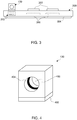
- FIG. 4 shows an example of the connector block 130 adapted to be mounted on the PCB 200 (shown in FIGS. 2-3 ).
- the connector block 130 can include a cuboidal structure having a through opening 400 sized to receive the lead terminal 126 (shown in FIG. 1 ) of the implantable lead 104 therein.
- the connector block 130 can include a rectangular cuboid structure or cylindrical structure having a through opening, such as the opening 400, configured to receive the lead terminal 126 therein.
- the connector block 130 can be made of metal to form a metallic housing.
- the connector block 130 can be mounted directly onto the PCB 200.
- the connector block 130 can include a gold plated plate 402, which may help in mounting the connector block 130 onto the PCB 200.
- the gold plated plate 402 at its one side, can be attached to the connector block 130 and, at the other side, can be attached to the PCB 200.
- one side of the gold plated plate 402 can be spot welded to the metallic housing of the connector block 130 and the other side of the gold plated plate 402 can be soldered or spot welded to the conductive traces of the PCB 200.
- the side of the gold plated plate 402 that is spot welded to the metallic housing of the connector block 130 lacks gold (e.g., the gold can be removed) for better spot welding.
- the other side of the gold plated plate 402 that is soldered or spot welded to the PCB 200 can have gold.
- the substrate plate of the gold plated plate 402 can be a nickel-cobalt ferrous alloy or a Fe-Ni alloy, such as Kovar, for example.
- the connector block 130 can include a contact spring 404 disposed within the metallic housing.
- the connector block 130 can include an intermediate indented portion (not shown) adapted to receive the contact spring 404 therein.
- the contact spring 404 can be an electrically conductive flexible ring configured to contact a conductive portion of the lead terminal 126, when the lead terminal 126 is received within the opening 400 of the connector block 130.
- the contact spring 404 can facilitate in establishing electrical connection between the implantable lead 104 and the IMD 102.
- the contact spring 404 can be diametrically smaller as compared to the lead terminal 126 and due to the flexible nature of the contact spring 404; the contact spring 404 can help in holding the lead terminal 126 in place within the opening 400 and the port 110.
- the lead terminal 126 can include a locking feature (e.g., structural configuration) that can help in mechanically locking the lead terminal 126 with the IMD 102. It may be evident that the apparatus 100 may include one or more such connector blocks similar to the block 130 disposed in the single port 110 for providing electrical and mechanical connection between the IMD 102 and the implantable lead 104.
- a locking feature e.g., structural configuration
- the apparatus 100 may include one or more such connector blocks similar to the block 130 disposed in the single port 110 for providing electrical and mechanical connection between the IMD 102 and the implantable lead 104.
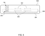
- FIG. 5 shows an example of the IMD 102 having a body 500.
- the body 500 encapsulates the PCB 200, the connector block 130 mounted directly onto the PCB 200, the electronic components 302 mounted on the PCB 200, and the power supply 304 coupled to the PCB 200.
- the body 500 can be formed by an overmolded polymer material that provides hermetic sealing.
- the polymer material can include a biocompatible material, such as parylene, polytetrafluoroethylene, ethylene tetrafluoroethylene, polyimide, polyurethane, silicone, and aromatic polyester polymers, i.e. liquid crystal polymers.
- the polymer material can be injection molded, extruded or co-extruded instead of overmolding to form the encapsulated polymeric body 500 for the IMD 102.
- the body 500 may be configured to have one or more ports, such as the port 110, to provide access to the connector block 130 for the lead terminal 126.
- the body 500 of the present disclosure can replace a typical bio compatible metal casing, such as a titanium casing, that hermetically seals a conventional IMD.
- the body 500 can be capable of providing hermetic sealing to the IMD 102.
- the body 500 can provide capabilities to the IMD 102 to be used in more demanding environments where moisture and other contaminants are prevalent.
- the PCB 200, the connector block 130, the electronic components 302 and the power supply 304 can be coated/sealed with a liquid crystal polymer using an injection molding process or any other process.
- the apparatus 100 may include a moisture sensor for providing information pertaining to moisture accumulation/formation within the IMD 102 so as to take corrective measures against moisture accumulation/formation.
- FIG. 6 is a diagram of a method 600 for assembling an implantable medical device (IMD), such as the IMD 102.
- IMD implantable medical device
- a filter capacitor such as the filter capacitor 202
- the filter capacitor can be inserted within the PCB during the time of PCB manufacture process.
- the filter capacitor 202 may be inserted within the PCB 200 using an ECP process.
- the PCB can include two layers with a cavity or recess adapted to receive the filter capacitor therein. The two layers of the PCB can be thereafter thermally and/or mechanically pressed for embedding the filter capacitor therewithin.
- one or more electronic elements such as integrated circuits 300, may be embedded within the body of the PCB.
- one or more electronic elements such as the electronic components 302, for example, or one or more diodes, amplifiers, transistors, oscillators, resistors, capacitors, inductors, transformers, RF transmitter/receiver, or interconnects, can be directly mounted onto the PCB.
- the electronic components either mounted on or received with the PCB, can perform signal analysis for providing electric therapy to a patient's body.
- the IMD can also include a power supply, such as a battery, adapted to supply electrical power to the electronic components for allowing the electronic component to perform one or more operations associated with the IMD.
- a connector block such as the connector block 130, for a lead terminal, such as the lead terminal 126, of the IMD can be mounted directly to the PCB 200.
- the filter capacitor 202 can be located beneath the connector block 130.
- the connector block can be a metallic cuboidal housing having a through opening, such as the opening 400.
- the opening 400 can be sized to receive therein the lead terminal of an implantable lead, such as the implantable lead 104, for establishing mechanical and electrical connection between the IMD and the implantable lead.
- the connector block can be mounted directly onto the PCB with the help of a gold plated plate, such as the gold plated plate 402.
- the gold plated plate on its one side can be spot welded to the connector block, and on its other side can be soldered or spot welded to the PCB.
- the connector block and the printed circuit board can be encapsulated with an overmolded polymer material.
- the PCB, the connector block and the electronic components mounted on the PCB, and the power supply coupled to the PCB can be encapsulated (e.g., hermetically sealed) within an overmolded polymer material.
- the polymer material may include biocompatible material, such as parylene, polytetrafluoroethylene, ethylene tetrafluoroethylene, polyimide, polyurethane, silicone, and aromatic polyester polymers, i.e. liquid crystal polymers.
- the polymer material may be injection molded, extruded or co-extruded instead of overmolded to form an encapsulated body. It is to be understood that during encapsulation one or more ports, such as the port 110, can be provided for the lead terminal to access the connector block.
- the apparatus 100 and the method 600 described herein can facilitate in reducing manufacturing process steps involved in an assembling process of an IMD. This can reduce the IMD manufacturing cost and time.
- the apparatus 100 and the method 600 can preclude a need for a conventional feed-through terminal pin assembly, since a connector block can be directly mounted on the PCB.
- a filter capacitor can be inserted within the PCB as an integral part of the PCB during manufacturing of the PCB, which can preclude a need for separately coupling a conventional filter capacitor with a conventional feed-through terminal pin assembly.
- fewer electronic components can also be inserted within the PCB giving more available free surface area for additional electronic components to be mounted onto the PCB.
- inserting the electronic components within the PCB provides compact design (miniaturization) for the IMD. This can improve electrical and thermal performance of the electronic components. This can help in saving in expensive component packaging and shielding measures, and can help in reducing PCB complexities.
Claims (11)
- Gerät, umfassend:eine implantierbare medizinische Vorrichtung (102), aufweisend:eine gedruckte Leiterplatte (200), die einen Körper aufweist;einen Anschluss (110) zum Bereitstellen einer elektrischen und medizinischen Verbindung zwischen der implantierbaren mechanischen Vorrichtung (102) und einem implantierbaren Anschlusselement (104), wobei das implantierbare Anschlusselement (104) konfiguriert ist, um elektrische Signale zwischen der implantierbaren medizinischen Vorrichtung (102) und einem Zielgewebe zu transportieren; undeinen Steckverbinderblock (130) der in dem Anschluss (110) angeordnet ist,wobei der Steckverbinderblock (130) so dimensioniert ist, dass eine Anschlusselementklemme (126) des implantierbaren Anschlusselements (104) in den Steckverbinderblock (130) eingefügt werden und von diesem aufgenommen werden kann,wobei der Steckverbinderblock (130) direkt auf die gedruckte Leiterplatte montiert ist,wobei das Gerät außerdem einen Filterkondensator (202) umfasst, der in dem Körper der gedruckten Leiterplatte (200) angebracht ist und unter dem Steckverbinderblock (130) angebracht ist, undwobei der Steckverbinderblock (130) und die gedruckte Leiterplatte (200) in ein überspritztes Polymermaterial eingekapselt sind.
- Gerät nach Anspruch 1, wobei der Filterkondensator (202) eine Vielzahl von Plattenschichten (210, 212) aufweist, die in den Körper der gedruckten Leiterplatte eingebettet (200) sind.
- Gerät nach Anspruch 1 bis 2, wobei die gedruckte Leiterplatte (200) eine Vielzahl von laminierten Schichten aufweist, wobei mindestens eine Schicht über dem Filterkondensator (202) angebracht ist und mindestens eine Schicht unter dem Kondensator (202) angebracht ist.
- Gerät nach einem der Ansprüche 1 bis 3, wobei der Steckverbinderblock (130) eine goldplattierte Platte (402) aufweist, die an einer Seite befestigt ist, die an die gedruckte Leiterplatte (200) gelötet oder punktgeschweißt ist.
- Gerät nach einem der Ansprüche 1 bis 4, wobei die gedruckte Leiterplatte (200) außerdem einen oder mehrere integrierte Schaltkreise (300) aufweist, die in den Körper der gedruckten Leiterplatte eingebettet (200) sind.
- Gerät nach einem der Ansprüche 1 bis 5, das außerdem eine oder mehrere elektronische Komponenten (302) aufweist, die mit der gedruckten Leiterplatte verbunden sind und die konfiguriert sind, um eine Signalanalyse auszuführen, um einem Körper eine Elektrotherapie bereitzustellen, und das außerdem eine Stromversorgung aufweist, die mit der gedruckten Leiterplatte (200) verbunden ist.
- Vorrichtung nach Anspruch 6, wobei der Steckverbinderblock (130), die gedruckte Leiterplatte (200), die eine oder mehreren elektronischen Komponenten (302) und die Stromversorgung in ein überspritztes Polymermaterial eingekapselt sind.
- Gerät nach Anspruch 7, das einen oder mehrere Anschlüsse (110) in dem überspritzten Polymermaterial aufweist, um einen Zugriff auf den Steckverbinderblock (130) für die Anschlusselementklemme (126) bereitzustellen.
- Gerät nach einem der Ansprüche 1 bis 8, wobei der Steckverbinderblock (130) ein metallisches Gehäuse und eine Kontaktfeder (404) in dem Gehäuse aufweist, um die Anschlusselementklemme (126) aufzunehmen.
- Verfahren, umfassend:Verbinden eines Steckverbinderblocks (130) für eine Anschlusselementklemme (126) des implantierbaren Anschlusselements (104) einer implantierbaren medizinischen Vorrichtung direkt mit einer gedruckten Leiterplatte,wobei das implantierbare Anschlusselement (104) konfiguriert ist, um elektrische Signale zwischen der implantierbaren medizinischen Vorrichtung (102) und einem Zielgewebe zu transportieren; undwobei der Steckverbinderblock (130) so dimensioniert ist, dass die Anschlusselementklemme (126) des implantierbaren Anschlusselements (104) in den Steckverbinderblock (130) eingefügt werden und von diesem aufgenommen werden kann;Bereitstellen eines Filterkondensators (202) in einem Körper der gedruckten Leiterplatte (200) und unter dem Steckverbinderblock; undEinkapseln des Steckverbinderblocks (130) und der gedruckten Leiterplatte (200) in ein überspritztes Polymermaterial.
- Verfahren nach Anspruch 10, wobei das Verbinden des Steckverbinderblocks (130) ein Verbinden einer goldplattierten Platte (402) an dem Steckverbinderblock (130) mit einer Leiterbahn der gedruckten Leiterplatte (200) umfasst.
Priority Applications (1)
| Application Number | Priority Date | Filing Date | Title |
|---|---|---|---|
| EP18200104.0A EP3446748B1 (de) | 2013-03-12 | 2014-02-06 | Implantierbare medizinische vorrichtung und montage davon |
Applications Claiming Priority (2)
| Application Number | Priority Date | Filing Date | Title |
|---|---|---|---|
| US201361777473P | 2013-03-12 | 2013-03-12 | |
| PCT/US2014/015107 WO2014143460A1 (en) | 2013-03-12 | 2014-02-06 | Implantable medical device and assembly thereof |
Related Child Applications (1)
| Application Number | Title | Priority Date | Filing Date |
|---|---|---|---|
| EP18200104.0A Division EP3446748B1 (de) | 2013-03-12 | 2014-02-06 | Implantierbare medizinische vorrichtung und montage davon |
Publications (2)
| Publication Number | Publication Date |
|---|---|
| EP2968953A1 EP2968953A1 (de) | 2016-01-20 |
| EP2968953B1 true EP2968953B1 (de) | 2018-10-17 |
Family
ID=50159555
Family Applications (2)
| Application Number | Title | Priority Date | Filing Date |
|---|---|---|---|
| EP18200104.0A Active EP3446748B1 (de) | 2013-03-12 | 2014-02-06 | Implantierbare medizinische vorrichtung und montage davon |
| EP14706410.9A Active EP2968953B1 (de) | 2013-03-12 | 2014-02-06 | Implantierbare medizinische vorrichtung und montage davon |
Family Applications Before (1)
| Application Number | Title | Priority Date | Filing Date |
|---|---|---|---|
| EP18200104.0A Active EP3446748B1 (de) | 2013-03-12 | 2014-02-06 | Implantierbare medizinische vorrichtung und montage davon |
Country Status (6)
| Country | Link |
|---|---|
| US (1) | US10173053B2 (de) |
| EP (2) | EP3446748B1 (de) |
| JP (1) | JP6492049B2 (de) |
| CN (1) | CN105246545B (de) |
| AU (2) | AU2014228643A1 (de) |
| WO (1) | WO2014143460A1 (de) |
Families Citing this family (6)
| Publication number | Priority date | Publication date | Assignee | Title |
|---|---|---|---|---|
| JP6492049B2 (ja) | 2013-03-12 | 2019-03-27 | カーディアック ペースメイカーズ, インコーポレイテッド | 埋め込み型医療装置及びそのアセンブリ |
| US9713717B2 (en) * | 2013-12-09 | 2017-07-25 | Boston Scientific Neuromodulation Corporation | Implantable stimulator device having components embedded in a circuit board |
| US9579511B2 (en) * | 2014-12-15 | 2017-02-28 | Medtronic, Inc. | Medical device with surface mounted lead connector |
| DE102016216997A1 (de) * | 2016-03-29 | 2017-10-05 | Continental Teves Ag & Co. Ohg | Fahrzeugkommunikationsmodul |
| EP4319865A1 (de) * | 2021-04-08 | 2024-02-14 | Medtronic, Inc. | Implantierbare medizinische vorrichtung und system damit |
| WO2023119014A1 (en) * | 2021-12-20 | 2023-06-29 | Medtronic, Inc. | Implantable medical device and method of forming same |
Family Cites Families (15)
| Publication number | Priority date | Publication date | Assignee | Title |
|---|---|---|---|---|
| US4848346A (en) | 1987-12-02 | 1989-07-18 | Siemens-Pacesetter, Inc. | Pacemaker connector system |
| US5324311A (en) * | 1992-09-04 | 1994-06-28 | Siemens Pacesetter, Inc. | Coaxial bipolar connector assembly for implantable medical device |
| JP2867985B2 (ja) | 1996-12-20 | 1999-03-10 | 日本電気株式会社 | プリント回路基板 |
| US5963429A (en) | 1997-08-20 | 1999-10-05 | Sulzer Intermedics Inc. | Printed circuit substrate with cavities for encapsulating integrated circuits |
| US5973906A (en) * | 1998-03-17 | 1999-10-26 | Maxwell Energy Products, Inc. | Chip capacitors and chip capacitor electromagnetic interference filters |
| US6288344B1 (en) | 1999-08-20 | 2001-09-11 | Cardiac Pacemakers, Inc. | Integrated EMI shield utilizing a hybrid edge |
| US6498951B1 (en) | 2000-10-13 | 2002-12-24 | Medtronic, Inc. | Implantable medical device employing integral housing for a formable flat battery |
| WO2004052452A1 (en) | 2002-12-09 | 2004-06-24 | Medtronic, Inc. | Reducing relative intermodule motion in a modular implantable medical device |
| US7322832B2 (en) * | 2004-10-26 | 2008-01-29 | Medtronic, Inc. | Radio frequency antenna flexible circuit interconnect with unique micro connectors |
| US7128801B2 (en) | 2005-02-03 | 2006-10-31 | Harris Corporation | Method and apparatus for sealing flex circuits having heat sensitive circuit elements |
| EP2520331A3 (de) | 2006-04-12 | 2013-02-20 | Proteus Digital Health, Inc. | Lückenfreie implantierbare, hermetisch verschlossene Strukturen |
| CN102037528A (zh) | 2008-03-20 | 2011-04-27 | 格瑞巴奇有限公司 | 屏蔽三端子平通emi/消能滤波器 |
| EP2529790B1 (de) * | 2011-06-03 | 2017-09-20 | Greatbatch Ltd. | Durchführungsdrahtverbinder zur Verwendung in einer medizinischen Vorrichtung |
| US9950180B2 (en) | 2012-04-27 | 2018-04-24 | Medtronic, Inc. | Implantable device with chassis element |
| JP6492049B2 (ja) | 2013-03-12 | 2019-03-27 | カーディアック ペースメイカーズ, インコーポレイテッド | 埋め込み型医療装置及びそのアセンブリ |
-
2014
- 2014-02-06 JP JP2016500210A patent/JP6492049B2/ja active Active
- 2014-02-06 WO PCT/US2014/015107 patent/WO2014143460A1/en active Application Filing
- 2014-02-06 EP EP18200104.0A patent/EP3446748B1/de active Active
- 2014-02-06 CN CN201480014458.0A patent/CN105246545B/zh active Active
- 2014-02-06 EP EP14706410.9A patent/EP2968953B1/de active Active
- 2014-02-06 US US14/174,478 patent/US10173053B2/en active Active
- 2014-02-06 AU AU2014228643A patent/AU2014228643A1/en not_active Abandoned
-
2017
- 2017-04-11 AU AU2017202387A patent/AU2017202387B2/en not_active Ceased
Non-Patent Citations (1)
| Title |
|---|
| None * |
Also Published As
| Publication number | Publication date |
|---|---|
| JP2016510631A (ja) | 2016-04-11 |
| CN105246545A (zh) | 2016-01-13 |
| EP2968953A1 (de) | 2016-01-20 |
| WO2014143460A1 (en) | 2014-09-18 |
| US20140277234A1 (en) | 2014-09-18 |
| CN105246545B (zh) | 2018-01-19 |
| AU2017202387A1 (en) | 2017-04-27 |
| AU2017202387B2 (en) | 2018-10-04 |
| AU2014228643A1 (en) | 2015-10-15 |
| US10173053B2 (en) | 2019-01-08 |
| JP6492049B2 (ja) | 2019-03-27 |
| EP3446748B1 (de) | 2019-10-23 |
| EP3446748A1 (de) | 2019-02-27 |
Similar Documents
| Publication | Publication Date | Title |
|---|---|---|
| AU2017202387B2 (en) | Implantable medical device and assembly thereof | |
| US6721602B2 (en) | Implantable medical device assembly and manufacturing method | |
| US8626310B2 (en) | External RF telemetry module for implantable medical devices | |
| US8676321B2 (en) | Connection housing and manufacture of same | |
| US7035077B2 (en) | Device to protect an active implantable medical device feedthrough capacitor from stray laser weld strikes, and related manufacturing process | |
| CN106029168B (zh) | 用于可植入医疗装置的经滤波的馈通组件 | |
| AU2016243089B2 (en) | Encapsulated filtered feedthrough for implantable medical devices | |
| US8843215B2 (en) | Connecting device | |
| US8706228B2 (en) | Electronic module assembly for filtered feedthroughs | |
| US7214068B2 (en) | Laser ribbon bond pad array connector | |
| US20160271401A1 (en) | Implantable Medical Device and Manufacturing Method Therefor | |
| US10071253B2 (en) | Implantable device with internal lead connector |
Legal Events
| Date | Code | Title | Description |
|---|---|---|---|
| PUAI | Public reference made under article 153(3) epc to a published international application that has entered the european phase |
Free format text: ORIGINAL CODE: 0009012 |
|
| 17P | Request for examination filed |
Effective date: 20150928 |
|
| AK | Designated contracting states |
Kind code of ref document: A1 Designated state(s): AL AT BE BG CH CY CZ DE DK EE ES FI FR GB GR HR HU IE IS IT LI LT LU LV MC MK MT NL NO PL PT RO RS SE SI SK SM TR |
|
| AX | Request for extension of the european patent |
Extension state: BA ME |
|
| DAX | Request for extension of the european patent (deleted) | ||
| GRAP | Despatch of communication of intention to grant a patent |
Free format text: ORIGINAL CODE: EPIDOSNIGR1 |
|
| STAA | Information on the status of an ep patent application or granted ep patent |
Free format text: STATUS: GRANT OF PATENT IS INTENDED |
|
| INTG | Intention to grant announced |
Effective date: 20170301 |
|
| GRAJ | Information related to disapproval of communication of intention to grant by the applicant or resumption of examination proceedings by the epo deleted |
Free format text: ORIGINAL CODE: EPIDOSDIGR1 |
|
| STAA | Information on the status of an ep patent application or granted ep patent |
Free format text: STATUS: REQUEST FOR EXAMINATION WAS MADE |
|
| INTC | Intention to grant announced (deleted) | ||
| STAA | Information on the status of an ep patent application or granted ep patent |
Free format text: STATUS: EXAMINATION IS IN PROGRESS |
|
| 17Q | First examination report despatched |
Effective date: 20170630 |
|
| GRAP | Despatch of communication of intention to grant a patent |
Free format text: ORIGINAL CODE: EPIDOSNIGR1 |
|
| STAA | Information on the status of an ep patent application or granted ep patent |
Free format text: STATUS: GRANT OF PATENT IS INTENDED |
|
| INTG | Intention to grant announced |
Effective date: 20180502 |
|
| GRAS | Grant fee paid |
Free format text: ORIGINAL CODE: EPIDOSNIGR3 |
|
| GRAA | (expected) grant |
Free format text: ORIGINAL CODE: 0009210 |
|
| STAA | Information on the status of an ep patent application or granted ep patent |
Free format text: STATUS: THE PATENT HAS BEEN GRANTED |
|
| AK | Designated contracting states |
Kind code of ref document: B1 Designated state(s): AL AT BE BG CH CY CZ DE DK EE ES FI FR GB GR HR HU IE IS IT LI LT LU LV MC MK MT NL NO PL PT RO RS SE SI SK SM TR |
|
| REG | Reference to a national code |
Ref country code: GB Ref legal event code: FG4D |
|
| REG | Reference to a national code |
Ref country code: CH Ref legal event code: EP |
|
| REG | Reference to a national code |
Ref country code: IE Ref legal event code: FG4D |
|
| REG | Reference to a national code |
Ref country code: DE Ref legal event code: R096 Ref document number: 602014034189 Country of ref document: DE Ref country code: AT Ref legal event code: REF Ref document number: 1053288 Country of ref document: AT Kind code of ref document: T Effective date: 20181115 |
|
| REG | Reference to a national code |
Ref country code: NL Ref legal event code: FP |
|
| REG | Reference to a national code |
Ref country code: LT Ref legal event code: MG4D |
|
| REG | Reference to a national code |
Ref country code: AT Ref legal event code: MK05 Ref document number: 1053288 Country of ref document: AT Kind code of ref document: T Effective date: 20181017 |
|
| PG25 | Lapsed in a contracting state [announced via postgrant information from national office to epo] |
Ref country code: FI Free format text: LAPSE BECAUSE OF FAILURE TO SUBMIT A TRANSLATION OF THE DESCRIPTION OR TO PAY THE FEE WITHIN THE PRESCRIBED TIME-LIMIT Effective date: 20181017 Ref country code: LV Free format text: LAPSE BECAUSE OF FAILURE TO SUBMIT A TRANSLATION OF THE DESCRIPTION OR TO PAY THE FEE WITHIN THE PRESCRIBED TIME-LIMIT Effective date: 20181017 Ref country code: AT Free format text: LAPSE BECAUSE OF FAILURE TO SUBMIT A TRANSLATION OF THE DESCRIPTION OR TO PAY THE FEE WITHIN THE PRESCRIBED TIME-LIMIT Effective date: 20181017 Ref country code: PL Free format text: LAPSE BECAUSE OF FAILURE TO SUBMIT A TRANSLATION OF THE DESCRIPTION OR TO PAY THE FEE WITHIN THE PRESCRIBED TIME-LIMIT Effective date: 20181017 Ref country code: HR Free format text: LAPSE BECAUSE OF FAILURE TO SUBMIT A TRANSLATION OF THE DESCRIPTION OR TO PAY THE FEE WITHIN THE PRESCRIBED TIME-LIMIT Effective date: 20181017 Ref country code: BG Free format text: LAPSE BECAUSE OF FAILURE TO SUBMIT A TRANSLATION OF THE DESCRIPTION OR TO PAY THE FEE WITHIN THE PRESCRIBED TIME-LIMIT Effective date: 20190117 Ref country code: ES Free format text: LAPSE BECAUSE OF FAILURE TO SUBMIT A TRANSLATION OF THE DESCRIPTION OR TO PAY THE FEE WITHIN THE PRESCRIBED TIME-LIMIT Effective date: 20181017 Ref country code: LT Free format text: LAPSE BECAUSE OF FAILURE TO SUBMIT A TRANSLATION OF THE DESCRIPTION OR TO PAY THE FEE WITHIN THE PRESCRIBED TIME-LIMIT Effective date: 20181017 Ref country code: NO Free format text: LAPSE BECAUSE OF FAILURE TO SUBMIT A TRANSLATION OF THE DESCRIPTION OR TO PAY THE FEE WITHIN THE PRESCRIBED TIME-LIMIT Effective date: 20190117 Ref country code: IS Free format text: LAPSE BECAUSE OF FAILURE TO SUBMIT A TRANSLATION OF THE DESCRIPTION OR TO PAY THE FEE WITHIN THE PRESCRIBED TIME-LIMIT Effective date: 20190217 |
|
| PG25 | Lapsed in a contracting state [announced via postgrant information from national office to epo] |
Ref country code: AL Free format text: LAPSE BECAUSE OF FAILURE TO SUBMIT A TRANSLATION OF THE DESCRIPTION OR TO PAY THE FEE WITHIN THE PRESCRIBED TIME-LIMIT Effective date: 20181017 Ref country code: PT Free format text: LAPSE BECAUSE OF FAILURE TO SUBMIT A TRANSLATION OF THE DESCRIPTION OR TO PAY THE FEE WITHIN THE PRESCRIBED TIME-LIMIT Effective date: 20190217 Ref country code: GR Free format text: LAPSE BECAUSE OF FAILURE TO SUBMIT A TRANSLATION OF THE DESCRIPTION OR TO PAY THE FEE WITHIN THE PRESCRIBED TIME-LIMIT Effective date: 20190118 Ref country code: RS Free format text: LAPSE BECAUSE OF FAILURE TO SUBMIT A TRANSLATION OF THE DESCRIPTION OR TO PAY THE FEE WITHIN THE PRESCRIBED TIME-LIMIT Effective date: 20181017 Ref country code: SE Free format text: LAPSE BECAUSE OF FAILURE TO SUBMIT A TRANSLATION OF THE DESCRIPTION OR TO PAY THE FEE WITHIN THE PRESCRIBED TIME-LIMIT Effective date: 20181017 |
|
| REG | Reference to a national code |
Ref country code: DE Ref legal event code: R097 Ref document number: 602014034189 Country of ref document: DE |
|
| PG25 | Lapsed in a contracting state [announced via postgrant information from national office to epo] |
Ref country code: CZ Free format text: LAPSE BECAUSE OF FAILURE TO SUBMIT A TRANSLATION OF THE DESCRIPTION OR TO PAY THE FEE WITHIN THE PRESCRIBED TIME-LIMIT Effective date: 20181017 Ref country code: DK Free format text: LAPSE BECAUSE OF FAILURE TO SUBMIT A TRANSLATION OF THE DESCRIPTION OR TO PAY THE FEE WITHIN THE PRESCRIBED TIME-LIMIT Effective date: 20181017 |
|
| PLBE | No opposition filed within time limit |
Free format text: ORIGINAL CODE: 0009261 |
|
| STAA | Information on the status of an ep patent application or granted ep patent |
Free format text: STATUS: NO OPPOSITION FILED WITHIN TIME LIMIT |
|
| PG25 | Lapsed in a contracting state [announced via postgrant information from national office to epo] |
Ref country code: EE Free format text: LAPSE BECAUSE OF FAILURE TO SUBMIT A TRANSLATION OF THE DESCRIPTION OR TO PAY THE FEE WITHIN THE PRESCRIBED TIME-LIMIT Effective date: 20181017 Ref country code: SM Free format text: LAPSE BECAUSE OF FAILURE TO SUBMIT A TRANSLATION OF THE DESCRIPTION OR TO PAY THE FEE WITHIN THE PRESCRIBED TIME-LIMIT Effective date: 20181017 Ref country code: SK Free format text: LAPSE BECAUSE OF FAILURE TO SUBMIT A TRANSLATION OF THE DESCRIPTION OR TO PAY THE FEE WITHIN THE PRESCRIBED TIME-LIMIT Effective date: 20181017 Ref country code: RO Free format text: LAPSE BECAUSE OF FAILURE TO SUBMIT A TRANSLATION OF THE DESCRIPTION OR TO PAY THE FEE WITHIN THE PRESCRIBED TIME-LIMIT Effective date: 20181017 |
|
| 26N | No opposition filed |
Effective date: 20190718 |
|
| REG | Reference to a national code |
Ref country code: CH Ref legal event code: PL |
|
| PG25 | Lapsed in a contracting state [announced via postgrant information from national office to epo] |
Ref country code: LU Free format text: LAPSE BECAUSE OF NON-PAYMENT OF DUE FEES Effective date: 20190206 Ref country code: SI Free format text: LAPSE BECAUSE OF FAILURE TO SUBMIT A TRANSLATION OF THE DESCRIPTION OR TO PAY THE FEE WITHIN THE PRESCRIBED TIME-LIMIT Effective date: 20181017 Ref country code: MC Free format text: LAPSE BECAUSE OF FAILURE TO SUBMIT A TRANSLATION OF THE DESCRIPTION OR TO PAY THE FEE WITHIN THE PRESCRIBED TIME-LIMIT Effective date: 20181017 |
|
| REG | Reference to a national code |
Ref country code: BE Ref legal event code: MM Effective date: 20190228 |
|
| REG | Reference to a national code |
Ref country code: IE Ref legal event code: MM4A |
|
| PG25 | Lapsed in a contracting state [announced via postgrant information from national office to epo] |
Ref country code: CH Free format text: LAPSE BECAUSE OF NON-PAYMENT OF DUE FEES Effective date: 20190228 Ref country code: LI Free format text: LAPSE BECAUSE OF NON-PAYMENT OF DUE FEES Effective date: 20190228 |
|
| PG25 | Lapsed in a contracting state [announced via postgrant information from national office to epo] |
Ref country code: IE Free format text: LAPSE BECAUSE OF NON-PAYMENT OF DUE FEES Effective date: 20190206 |
|
| PG25 | Lapsed in a contracting state [announced via postgrant information from national office to epo] |
Ref country code: BE Free format text: LAPSE BECAUSE OF NON-PAYMENT OF DUE FEES Effective date: 20190228 |
|
| PG25 | Lapsed in a contracting state [announced via postgrant information from national office to epo] |
Ref country code: TR Free format text: LAPSE BECAUSE OF FAILURE TO SUBMIT A TRANSLATION OF THE DESCRIPTION OR TO PAY THE FEE WITHIN THE PRESCRIBED TIME-LIMIT Effective date: 20181017 |
|
| PGFP | Annual fee paid to national office [announced via postgrant information from national office to epo] |
Ref country code: IT Payment date: 20200128 Year of fee payment: 7 |
|
| PG25 | Lapsed in a contracting state [announced via postgrant information from national office to epo] |
Ref country code: MT Free format text: LAPSE BECAUSE OF NON-PAYMENT OF DUE FEES Effective date: 20190206 |
|
| PG25 | Lapsed in a contracting state [announced via postgrant information from national office to epo] |
Ref country code: CY Free format text: LAPSE BECAUSE OF FAILURE TO SUBMIT A TRANSLATION OF THE DESCRIPTION OR TO PAY THE FEE WITHIN THE PRESCRIBED TIME-LIMIT Effective date: 20181017 |
|
| PG25 | Lapsed in a contracting state [announced via postgrant information from national office to epo] |
Ref country code: HU Free format text: LAPSE BECAUSE OF FAILURE TO SUBMIT A TRANSLATION OF THE DESCRIPTION OR TO PAY THE FEE WITHIN THE PRESCRIBED TIME-LIMIT; INVALID AB INITIO Effective date: 20140206 |
|
| PG25 | Lapsed in a contracting state [announced via postgrant information from national office to epo] |
Ref country code: IT Free format text: LAPSE BECAUSE OF NON-PAYMENT OF DUE FEES Effective date: 20210206 |
|
| PG25 | Lapsed in a contracting state [announced via postgrant information from national office to epo] |
Ref country code: MK Free format text: LAPSE BECAUSE OF FAILURE TO SUBMIT A TRANSLATION OF THE DESCRIPTION OR TO PAY THE FEE WITHIN THE PRESCRIBED TIME-LIMIT Effective date: 20181017 |
|
| PGFP | Annual fee paid to national office [announced via postgrant information from national office to epo] |
Ref country code: FR Payment date: 20230119 Year of fee payment: 10 |
|
| PGFP | Annual fee paid to national office [announced via postgrant information from national office to epo] |
Ref country code: GB Payment date: 20230121 Year of fee payment: 10 Ref country code: DE Payment date: 20230119 Year of fee payment: 10 |
|
| PGFP | Annual fee paid to national office [announced via postgrant information from national office to epo] |
Ref country code: NL Payment date: 20230119 Year of fee payment: 10 |
|
| PGFP | Annual fee paid to national office [announced via postgrant information from national office to epo] |
Ref country code: NL Payment date: 20240123 Year of fee payment: 11 |