EP2966736A1 - Semiconductor laser module and production method for same - Google Patents
Semiconductor laser module and production method for same Download PDFInfo
- Publication number
- EP2966736A1 EP2966736A1 EP14759748.8A EP14759748A EP2966736A1 EP 2966736 A1 EP2966736 A1 EP 2966736A1 EP 14759748 A EP14759748 A EP 14759748A EP 2966736 A1 EP2966736 A1 EP 2966736A1
- Authority
- EP
- European Patent Office
- Prior art keywords
- lens
- semiconductor laser
- along
- fixation
- resin
- Prior art date
- Legal status (The legal status is an assumption and is not a legal conclusion. Google has not performed a legal analysis and makes no representation as to the accuracy of the status listed.)
- Withdrawn
Links
- 239000004065 semiconductor Substances 0.000 title claims abstract description 155
- 238000004519 manufacturing process Methods 0.000 title claims description 17
- 229920005989 resin Polymers 0.000 claims abstract description 165
- 239000011347 resin Substances 0.000 claims abstract description 165
- 239000000758 substrate Substances 0.000 claims abstract description 78
- 230000003287 optical effect Effects 0.000 claims abstract description 10
- 125000006850 spacer group Chemical group 0.000 claims description 21
- 229920001187 thermosetting polymer Polymers 0.000 claims description 8
- 239000013307 optical fiber Substances 0.000 description 11
- 239000011521 glass Substances 0.000 description 6
- 239000003822 epoxy resin Substances 0.000 description 5
- 229920000647 polyepoxide Polymers 0.000 description 5
- 238000005219 brazing Methods 0.000 description 3
- 238000010586 diagram Methods 0.000 description 3
- 238000000034 method Methods 0.000 description 2
- 229910000679 solder Inorganic materials 0.000 description 2
- 230000000694 effects Effects 0.000 description 1
Images




Classifications
-
- H—ELECTRICITY
- H01—ELECTRIC ELEMENTS
- H01S—DEVICES USING THE PROCESS OF LIGHT AMPLIFICATION BY STIMULATED EMISSION OF RADIATION [LASER] TO AMPLIFY OR GENERATE LIGHT; DEVICES USING STIMULATED EMISSION OF ELECTROMAGNETIC RADIATION IN WAVE RANGES OTHER THAN OPTICAL
- H01S5/00—Semiconductor lasers
- H01S5/02—Structural details or components not essential to laser action
- H01S5/022—Mountings; Housings
- H01S5/0225—Out-coupling of light
- H01S5/02253—Out-coupling of light using lenses
-
- H—ELECTRICITY
- H01—ELECTRIC ELEMENTS
- H01S—DEVICES USING THE PROCESS OF LIGHT AMPLIFICATION BY STIMULATED EMISSION OF RADIATION [LASER] TO AMPLIFY OR GENERATE LIGHT; DEVICES USING STIMULATED EMISSION OF ELECTROMAGNETIC RADIATION IN WAVE RANGES OTHER THAN OPTICAL
- H01S5/00—Semiconductor lasers
- H01S5/02—Structural details or components not essential to laser action
- H01S5/022—Mountings; Housings
- H01S5/023—Mount members, e.g. sub-mount members
- H01S5/02325—Mechanically integrated components on mount members or optical micro-benches
- H01S5/02326—Arrangements for relative positioning of laser diodes and optical components, e.g. grooves in the mount to fix optical fibres or lenses
-
- G—PHYSICS
- G02—OPTICS
- G02B—OPTICAL ELEMENTS, SYSTEMS OR APPARATUS
- G02B19/00—Condensers, e.g. light collectors or similar non-imaging optics
- G02B19/0033—Condensers, e.g. light collectors or similar non-imaging optics characterised by the use
- G02B19/0047—Condensers, e.g. light collectors or similar non-imaging optics characterised by the use for use with a light source
- G02B19/0052—Condensers, e.g. light collectors or similar non-imaging optics characterised by the use for use with a light source the light source comprising a laser diode
-
- G—PHYSICS
- G02—OPTICS
- G02B—OPTICAL ELEMENTS, SYSTEMS OR APPARATUS
- G02B27/00—Optical systems or apparatus not provided for by any of the groups G02B1/00 - G02B26/00, G02B30/00
- G02B27/09—Beam shaping, e.g. changing the cross-sectional area, not otherwise provided for
- G02B27/0938—Using specific optical elements
- G02B27/095—Refractive optical elements
- G02B27/0955—Lenses
Definitions
- the present invention relates to a semiconductor laser module and a method of manufacturing the same. More particularly, the present invention relates to a semiconductor laser module including a semiconductor laser device and a collimator lens for collimating a laser beam emitted from the semiconductor laser device and to a method of manufacturing such a semiconductor laser module.
- a direction perpendicular to a p-n junction of a semiconductor laser device is referred to as a fast axis
- a direction in parallel to the p-n junction is referred to as a slow axis.
- a numerical aperture of a semiconductor laser device in a direction along its fast axis is much greater than that in a direction along its slow axis. Therefore, a laser beam emitted from a semiconductor laser device greatly spreads in a direction along its fast axis.
- a collimator lens for collimating fast-axis components of a laser beam emitted from a semiconductor laser device should be arranged near an emitting surface of the semiconductor laser device (see, e.g., Patent Literature 1 and Patent Literature 2).
- the collimator lens In order to arrange a desired optical system using such a collimator lens, it is necessary to fix the collimator lens highly precisely relative to a semiconductor laser device in a direction parallel to an optical axis and a direction parallel to a fast axis and to prevent variations in positional relationship between the semiconductor laser device and the collimator lens. Specifically, the positional relationship between the semiconductor laser device and the collimator lens should be fixed and maintained in the micron order.
- a collimator lens (optical fiber lens 26) is attached so that it can slide along its axis.
- a certain clearance needs to be formed between a cylindrical clamp 52 and the optical fiber lens 26. Therefore, variation in position of the optical fiber lens 26 cannot be reduced in the micron order in both of a direction of an optical axis of a laser beam emitted from a semiconductor laser device bar 10 and a direction along a fast axis.
- the optical fiber lens 26 of Patent Literature 1 is fixed to an attachment member 40 with an epoxy resin 50.
- the optical fiber lens 26 is deviated in the direction of the optical axis of the laser beam by shrinkage of the epoxy resin 50 on curing.
- the optical fiber lens 26 is fixed directly to the attachment member 40 with the epoxy resin 50, the amount of the epoxy resin 50 that is not less than required for alignment needs to be provided between the attachment member 40 and the optical fiber lens 26 in order to conduct alignment of the optical fiber lens 26.
- the optical fiber lens 26 is also deviated in a direction along its fast axis by shrinkage or expansion of the epoxy resin 50 due to a temperature change or a humidity change.
- Patent Literature 2 discloses a semiconductor laser module in which a semiconductor laser device 1 and a collimator lens 6 are fixed to one supplementary member 4 with brazing layers 5 and 8, respectively, to reduce variations in positional relationship between the semiconductor laser device 1 and the collimator lens 6 in cooperation with deflection of the semiconductor laser device 1 and deflection of the collimator lens 6.
- the semiconductor laser device 1 needs to be positioned at a high temperature of, for example, about 400°C in order to braze the brazing layers 5 and 8.
- a laser beam cannot be emitted from the semiconductor laser device 1 at such a high temperature.
- the collimator lens 6 cannot be aligned while a laser beam is emitted from the semiconductor laser device 1 (what is called active alignment cannot be performed).
- the present invention has been made in view of the above drawbacks in the prior art. It is, therefore, a first object of the present invention to provide a semiconductor laser module capable of reducing influence from shrinkage or expansion of a resin for fixing a collimator lens and of holding the collimator lens in a highly precisely aligned state.
- a second object of the present invention is to provide a method of manufacturing a semiconductor laser module that can fix a collimator lens with high precision relative to a semiconductor laser device while active alignment of the collimator lens is performed.
- a semiconductor laser module capable of reducing influence from shrinkage or expansion of a resin for fixing a collimator lens and of holding the collimator lens in a highly precisely aligned state.
- the semiconductor laser module has a substrate, a device-mounting portion provided on the substrate, and a semiconductor laser device mounted on the device-mounting portion.
- the semiconductor laser device emits a laser beam having an optical axis along a first direction.
- the semiconductor laser module has a collimator lens configured to collimate a component of the laser beam emitted from the semiconductor laser device along a second direction perpendicular to the first direction and a lens fixture block having a lens attachment surface perpendicular to a third direction that is perpendicular to the first direction and the second direction and a block fixation surface perpendicular to the third direction. At least one of ends of the collimator lens along the third direction is fixed to the lens attachment surface of the lens fixture block with a lens fixation resin.
- the block fixation surface of the lens fixture block is fixed to a side surface of the device-mounting portion along the third direction with a block fixation resin.
- the lens fixation resin for fixing the collimator lens is provided between the end of the collimator lens along the third direction and the lens attachment surface perpendicular to the third direction. Therefore, shrinkage of the lens fixation resin on curing or shrinkage or expansion of the lens fixation resin due to a temperature change or a humidity change primarily causes the position of the collimator lens to vary only in the third direction. Furthermore, the position of the collimator lens does not need to be adjusted in the third direction. Thus, in terms of optics, the collimator lens may be located at any position in the third direction.
- the thickness of the lens fixation resin between the collimator lens and the lens attachment surface can be reduced so as to reduce the amount of variation of the lens fixation resin per se due to shrinkage or expansion of the lens fixation resin. Accordingly, the collimator lens hardly changes its position in the first direction or the second direction. As a result, influence from shrinkage or expansion of the lens fixation resin for fixing the collimator lens can be reduced. Thus, the collimator lens can be held in a highly precisely aligned state.
- the block fixation resin for fixing the lens fixture block is provided between the block fixation surface of the lens fixture block, which is perpendicular to the third direction, and the side surface of the device-mounting portion along the third direction. Therefore, shrinkage or expansion of the block fixation resin primarily causes the position of the lens fixture block to vary only in the third direction. Furthermore, the position of the collimator lens does not need to be adjusted in the third direction. Thus, in terms of optics, the collimator lens may be located at any position in the third direction. Therefore, the thickness of the block fixation resin between the lens fixture block and the side surface of the device-mounting portion along the third direction can be reduced so as to reduce the amount of variation of the block fixation resin per se due to shrinkage or expansion of the block fixation resin.
- the lens fixture block hardly changes its position in the Y-direction or the Z-direction.
- the collimator lens which is fixed to the lens fixture block, hardly changes its position in the Y-direction or the Z-direction.
- the collimator lens can be held in a highly precisely aligned state.
- the second direction may be a direction along a fast axis of the laser beam emitted from the semiconductor laser device.
- a UV-curable resin or a thermosetting resin may be used as the lens fixation resin.
- a UV-curable resin or a thermosetting resin may be used as the block fixation resin.
- the device-mounting portion may include a mounting substrate on which the semiconductor laser device is mounted and a spacer having a certain thickness.
- the block fixation surface of the lens fixture block may be fixed to a side surface of the spacer of the device-mounting portion along the third direction with the block fixation resin.
- an equal amount of the lens fixation resin is present on opposite sides of the collimator lens along the first direction.
- the lens fixation resin equally shrinks or expands on the opposite sides of the collimator lens along the first direction so that the shrinkage or expansion is cancelled out on the opposite sides of the collimator lens along the first direction. Accordingly, shrinkage or expansion of the lens fixation resin exerts substantially no influence on the collimator lens along the first direction.
- an equal amount of the lens fixation resin is preferably present on opposite sides of the collimator lens along the second direction.
- the lens fixation resin equally shrinks or expands on the opposite sides of the collimator lens along the second direction so that the shrinkage or expansion is cancelled out on the opposite sides of the collimator lens along the second direction. Accordingly, shrinkage or expansion of the lens fixation resin exerts substantially no influence on the collimator lens along the second direction.
- the position of the lens attachment surface of the lens fixture block may be located farther away from the device-mounting portion than the position of the block fixation surface of the lens fixture block along the third direction.
- a groove may be formed between the lens attachment surface and the block fixation surface of the lens fixture block for preventing the lens fixation resin from being brought into contact with the device-mounting portion.
- a method of manufacturing a semiconductor laser module that can fix a collimator lens with high precision relative to a semiconductor laser device while active alignment of the collimator lens is performed.
- This manufacturing method produces a semiconductor laser module having a semiconductor laser device operable to emit a laser beam having an optical axis along a first direction and a collimator lens configured to collimate a component of the laser beam emitted from the semiconductor laser device along a second direction perpendicular to the first direction.
- the semiconductor laser device is mounted to a device-mounting portion, and the device-mounting portion is fixed to a substrate.
- a lens fixation resin is applied to a lens attachment surface formed on a lens fixture block.
- An end of the collimator lens along the third direction is inserted into the lens fixation resin applied to the lens attachment surface in a state in which the lens attachment surface is perpendicular to a third direction that is perpendicular to the first direction and the second direction.
- the lens fixation resin is hardened to fix the collimator lens to the lens fixture block.
- a block fixation resin is applied to a side surface of the device-mounting portion along the third direction.
- the lens fixture block is brought into contact with the block fixation resin.
- the collimator lens is positioned into a desired location while a laser beam is emitted from the semiconductor laser device. When the collimator lens has been positioned, the block fixation resin is hardened to fix the lens fixture block and the collimator lens relative to the device-mounting portion.
- the collimator lens is fixed to the lens fixture block with the lens fixation resin. Therefore, this method does not require to hold an atmosphere at a high temperature, unlike solder jointing disclosed in Patent Literature 2. Accordingly, the collimator lens can be positioned in place while a laser beam is emitted from the semiconductor laser device (active alignment). Additionally, the lens fixation resin is provided between the end of the collimator lens along the third direction and the lens attachment surface parallel to the laser beam (first direction). Therefore, shrinkage of the lens fixation resin on curing or shrinkage or expansion of the lens fixation resin due to a temperature change or a humidity change primarily causes the position of the collimator lens to vary only in the third direction.
- the position of the collimator lens does not need to be adjusted in the third direction.
- the collimator lens may be located at any position in the third direction. Therefore, the thickness of the lens fixation resin between the collimator lens and the lens attachment surface can be reduced so as to reduce the amount of variation of the lens fixation resin per se due to shrinkage or expansion of the lens fixation resin. Accordingly, the collimator lens hardly changes its position in the first direction or the second direction. As a result, the collimator lens can be fixed to the semiconductor laser device with high precision.
- the block fixation resin for fixing the lens fixture block is provided between the block fixation surface of the lens fixture block, which is perpendicular to the third direction, and the side surface of the device-mounting portion along the third direction. Therefore, shrinkage or expansion of the block fixation resin primarily causes the position of the lens fixture block to vary only in the third direction. Furthermore, the position of the collimator lens does not need to be adjusted in the third direction. Thus, in terms of optics, the collimator lens may be located at any position in the third direction. Therefore, the thickness of the block fixation resin between the lens fixture block and the side surface of the device-mounting portion along the third direction can be reduced so as to reduce the amount of variation of the block fixation resin per se due to shrinkage or expansion of the block fixation resin.
- the lens fixture block hardly changes its position in the Y-direction or the Z-direction.
- the collimator lens which is fixed to the lens fixture block, hardly changes its position in the Y-direction or the Z-direction.
- the collimator lens can be held in a highly precisely aligned state.
- the second direction may be a direction along a fast axis of the laser beam emitted from the semiconductor laser device.
- a UV-curable resin or a thermosetting resin may be used as the lens fixation resin.
- a UV-curable resin or a thermosetting resin may be used as the block fixation resin.
- the device-mounting portion may include a mounting substrate and a spacer having a certain thickness.
- the semiconductor laser device may be mounted on the mounting substrate, and the mounting substrate may be fixed to the spacer.
- the block fixation surface of the lens fixture block may be fixed to a side surface of the spacer of the device-mounting portion along the third direction with the block fixation resin.
- the block fixation resin may be applied to a side surface of the spacer along the third direction.
- the lens fixation resin when the end of the collimator lens is inserted into the lens fixation resin, it is preferable to equalize the amounts of the lens fixation resin present on opposite sides of the collimator lens along the first direction.
- the lens fixation resin equally shrinks or expands on the opposite sides of the collimator lens along the first direction so that the shrinkage or expansion is cancelled out on the opposite sides of the collimator lens along the first direction. Accordingly, shrinkage or expansion of the lens fixation resin exerts substantially no influence on the collimator lens along the first direction.
- the lens fixation resin equally shrinks or expands on the opposite sides of the collimator lens along the second direction so that the shrinkage or expansion is cancelled out on the opposite sides of the collimator lens along the second direction. Accordingly, shrinkage or expansion of the lens fixation resin exerts substantially no influence on the collimator lens along the second direction.
- a semiconductor laser module capable of reducing influence from shrinkage or expansion of a resin for fixing a collimator lens and of holding the collimator lens in a highly precisely aligned state. Furthermore, according to the present invention, there can be provided a method of manufacturing a semiconductor laser module that can fix a collimator lens with high precision relative to a semiconductor laser device while active alignment of the collimator lens is performed.
- Embodiments of a semiconductor laser module according to the present invention will be described in detail below with reference to Figs. 1 to 8 .
- the same or corresponding components are denoted by the same reference numerals in Figs. 1 to 8 so as to avoid redundant explanation.
- Fig. 1 is a plan view showing a semiconductor laser module 1 according to a first embodiment of the present invention
- Fig. 2 is a front view thereof
- Fig. 3 is a side view thereof.
- the semiconductor laser module 1 of this embodiment has a first substrate 10, a second substrate 20 (device-mounting portion) fixed onto the first substrate 10, a semiconductor laser device (laser diode) 30 mounted on the second substrate 20, and a collimator lens 40 for collimating a laser beam emitted from the semiconductor laser device 30.
- the semiconductor laser device 30 emits a laser beam L along the Z-direction.
- the Y-direction illustrated in Fig. 2 is parallel to a fast axis of the laser beam L.
- the collimator lens 40 collimates components of the laser beam L emitted from the semiconductor laser device 30 along a direction of the fast axis (Y-direction) to generate parallel rays.
- a surface of the collimator lens 40 into which the laser beam L is incident is in parallel to the Y-axis, and a surface of the collimator lens 40 from which the laser beam is outputted is convex.
- the collimator lens 40 extends along a direction of the slow axis of the laser beam L (X-direction).
- the collimator lens 40 has a length of about 2 mm along the X-direction.
- the collimator lens 40 is aligned to generate desired parallel rays and positioned highly precisely with respect to the Y-direction and the Z-direction.
- the semiconductor laser module 1 of the present embodiment has a lens fixture block 50 that is substantially in the form of a rectangular parallelepiped made of, for example, glass or the like.
- the lens fixture block 50 has a lens attachment surface 50A and a block fixation surface 50B, which are in parallel to an optical axis of the laser beam L.
- the lens attachment surface 50A and the block fixation surface 50B are coplanar with each other.
- the lens attachment surface 50A and the block fixation surface 50B are also configured to be in parallel to the fast axis (Y-direction) of the laser beam L, i.e., to be perpendicular to the X-direction.
- the block fixation surface 50B of the lens fixture block 50 is fixed to a side surface 20A of the second substrate 20 in the X-direction with a block fixation resin 52.
- the lens fixture block 50 is held out of contact with the first substrate 10.
- the lens fixture block 50 is cantilevered by the second substrate 20.
- UV-curable resins or thermosetting resins may be used as the block fixation resin 52.
- the collimator lens 40 has an end 40A along the X-direction that is fixed to the lens attachment surface 50A of the lens fixture block 50 with a lens fixation resin 42.
- the collimator lens 40 is held out of contact with the first substrate 10.
- the collimator lens 40 is cantilevered by the lens fixture block 50.
- UV-curable resins or thermosetting resins may be used as the lens fixation resin 42.
- the lens fixation resin 42 fixes the end 40A of the collimator lens 40 in the X-direction, the Y-direction, and the Z-direction.
- an equal amount of the lens fixation resin 42 is present on opposite sides of the collimator lens 40 along the Z-direction.
- an equal amount of the lens fixation resin 42 is preferably present on opposite sides of the collimator lens 40 along the Y-direction. Moreover, it is preferable to reduce the thickness of the lens fixation resin 42 between the collimator lens 40 and the lens attachment surface 50A.
- the lens fixation resin 42 for fixing the collimator lens 40 is provided between the end 40A of the collimator lens 40 along the X-direction and the lens attachment surface 50A, which is perpendicular to the X-direction. Therefore, shrinkage of the lens fixation resin 42 on curing or shrinkage or expansion of the lens fixation resin 42 due to a temperature change or a humidity change primarily causes the position of the collimator lens 40 to vary only in the X-direction, i.e., the direction of the slow axis. Furthermore, reduction in thickness of the lens fixation resin 42 between the collimator lens 40 and the lens attachment surface 50A can reduce the amount of variation of the lens fixation resin 42 per se due to shrinkage or expansion of the lens fixation resin 42. Therefore, the collimator lens 40 hardly changes its position in the Y-direction or the Z-direction. Accordingly, the collimator lens 40 can be held in a highly precisely aligned state.
- the entire end surface of the end 40A of the collimator lens 40 along the X-direction is fixed to the lens attachment surface 50A with the lens fixation resin 42. Nevertheless, at least part of the end surface of the end 40A of the collimator lens 40 along the X-direction may be fixed to the lens attachment surface 50A with the lens fixation resin 42.
- the lens fixation resin 42 when an equal amount of the lens fixation resin 42 is present on opposite sides of the collimator lens 40 along the Z-direction, the lens fixation resin 42 equally shrinks or expands on the opposite sides of the collimator lens 40 so that the shrinkage or expansion is cancelled out on the opposite sides of the collimator lens 40. Accordingly, shrinkage or expansion of the lens fixation resin 42 exerts substantially no influence on the collimator lens 40 along the Z-direction.
- the lens fixation resin 42 when an equal amount of the lens fixation resin 42 is present on opposite sides of the collimator lens 40 along the Y-direction, the lens fixation resin 42 equally shrinks or expands on the opposite sides of the collimator lens 40 so that the shrinkage or expansion is cancelled out on the opposite sides of the collimator lens 40. Accordingly, shrinkage or expansion of the lens fixation resin 42 exerts substantially no influence on the collimator lens 40 along the Y-direction.
- the block fixation resin 52 for fixing the lens fixture block 50 is provided between the block fixation surface 50B of the lens fixture block 50, which is perpendicular to the X-direction, and the side surface 20A of the second substrate 20 along the X-direction. Therefore, shrinkage or expansion of the block fixation resin 52 primarily causes the position of the lens fixture block 50 to vary only in the X-direction. Furthermore, reduction in thickness of the block fixation resin 52 between the block fixation surface 50B of the lens fixture block 50 and the side surface 20A of the second substrate 20 can reduce the amount of variation of the lens fixation resin 42 per se due to shrinkage or expansion of the lens fixation resin 42. Therefore, the lens fixture block 50 hardly changes its position in the Y-direction or the Z-direction. Accordingly, the collimator lens 40, which is fixed to the lens fixture block 50, hardly changes its position in the Y-direction or the Z-direction. Thus, the collimator lens 40 can be held in a highly precisely aligned state.
- a semiconductor laser device 30 is first mounted onto a second substrate 20 as a device-mounting portion. Then the second substrate 20 having the semiconductor laser device 30 mounted thereon is fixed onto a first substrate 10 ( Fig. 4 ).
- a lens fixation resin 42 is applied to the lens attachment surface 50A of the lens fixture block 50.
- An end 40A of a collimator lens 40 is inserted into the lens fixation resin 42 in a direction perpendicular to the lens attachment surface 50A ( Fig. 5 ).
- the lens fixation resin 42 is hardened to fix the collimator lens 40 to the lens fixture block 50.
- a block fixation resin 52 is applied to a side surface 20A of the second substrate 20. Then the lens fixture block 50 to which the collimator lens 40 has been fixed is brought into contact with a portion of the second substrate 20 to which the block fixation resin 52 has been applied ( Fig. 6 ). At that time, the lens fixture block 50 has a lens attachment surface 50A that is perpendicular to the X-direction.
- a laser beam is emitted from the semiconductor laser device 30.
- the lens fixture block 50 is moved so that the collimator lens 40 is positioned in place (active alignment).
- the block fixation resin 52 is hardened to fix the lens fixture block 50 to the second substrate 20. In this manner, a semiconductor laser module 1 is completed ( Fig. 1 ).
- the collimator lens 40 is fixed to the lens fixture block 50 with the lens fixation resin 42. Therefore, this method does not require to hold an atmosphere at a high temperature, unlike solder jointing disclosed in Patent Literature 2. Accordingly, the collimator lens 40 can be positioned in place while a laser beam is emitted from the semiconductor laser device 30 (active alignment).
- the end 40A of the collimator lens 40 along the X-direction is fixed to the lens attachment surface 50A of the lens fixture block 50, which is perpendicular to the X-direction. Therefore, shrinkage of the lens fixation resin 42 on curing or shrinkage or expansion of the lens fixation resin 42 due to a temperature change or a humidity change hardly causes the collimator lens 40 to change its position in the Y-direction or the Z-direction. Additionally, reduction in thickness of the lens fixation resin 42 between the collimator lens 40 and the lens attachment surface 50A can reduce the amount of variation of the lens fixation resin 42 per se due to shrinkage or expansion of the lens fixation resin 42. Accordingly, the collimator lens 40 can be held in a highly precisely aligned state.
- the block fixation surface 50B of the lens fixture block 50 which is perpendicular to the X-direction, is fixed to the side surface 20A of the second substrate 20 along the X-direction. Therefore, shrinkage of the block fixation resin 52 on curing or shrinkage or expansion of the block fixation resin 52 due to a temperature change or a humidity change hardly causes the lens fixture block 50 to change its position in the Y-direction or the Z-direction. Additionally, reduction in thickness of the block fixation resin 52 between the block fixation surface 50B of the lens fixture block 50 and the side surface 20A of the second substrate 20 can reduce the amount of variation of the block fixation resin 52 per se due to shrinkage or expansion of the block fixation resin 52. Accordingly, the collimator lens 40, which is fixed to the lens fixture block 50, hardly changes its position in the Y-direction or the Z-direction. As a result, the collimator lens 40 can be held in a highly precisely aligned state.
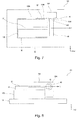
- Fig. 7 is a plan view showing a semiconductor laser module 101 according to a second embodiment of the present invention
- Fig. 8 is a front view of the semiconductor laser module 101
- Fig. 9 is a side view of the semiconductor laser module 101.
- the semiconductor laser module 101 of the present embodiment has a device-mounting portion on which a semiconductor laser device 30 is mounted.
- the device-mounting portion includes a second substrate 20, which is a mounting substrate on which the semiconductor laser device 30 is mounted, and a third substrate 120 as a spacer.
- Such a spacer 120 allows the semiconductor laser device 30 to be located at a desired height.
- the semiconductor laser module 101 of the present embodiment has a lens fixture block 150 that is substantially in the form of a rectangular parallelepiped made of, for example, glass or the like.
- This lens fixture block 150 has a lens attachment surface 150A and a block fixation surface 150B, which are perpendicular to the X-direction and coplanar with each other.
- the collimator lens 40 has an end 40A along the X-direction that is fixed to the lens attachment surface 150A with a lens fixation resin 42.
- the third substrate 120 has a side surface 120A along the X-direction that is fixed to the block fixation surface 150B of the lens fixture block 150 with a block fixation resin 52.
- the lens fixture block 150 is held out of contact with the first substrate 10. In other words, the lens fixture block 150 is cantilevered by the third substrate 120.
- a substrate on which the semiconductor laser device 30 is mounted often has a thickness of less than 0.5 mm along the fast axis direction (Y-direction). Therefore, in the aforementioned first embodiment, the width of the block fixation surface 50B of the lens fixture block 50 along the Y-direction is very small.
- the spacer 120 having an appropriate thickness is provided between the first substrate 10 and the second substrate 20 so that the lens fixture block 150 is fixed to the spacer 120, a sufficient area can be ensured in the block fixation surface 150B.
- the spacer 120 preferably has a thickness of 0.3 mm or more along the Y-direction.
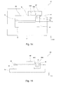
- Fig. 10 is a plan view showing a semiconductor laser module 201 according to a third embodiment of the present invention
- Fig. 11 is a front view of the semiconductor laser module 201.
- the semiconductor laser module 201 of the present embodiment has a lens fixture block 250 that is substantially in the form of a rectangular parallelepiped made of, for example, glass or the like.
- the lens fixture block 250 has a lens attachment surface 250A and a block fixation surface 250B, which are perpendicular to the X-direction.
- the position of the lens attachment surface 250A of the lens fixture block 250 is deviated from the position of the block fixation surface 250B along the X-direction. Therefore, the lens attachment surface 250A and the block fixation surface 250B form a step 250C.
- the collimator lens 40 has an end 40A along the X-direction that is fixed to the lens attachment surface 250A of the lens fixture block 250 with a lens fixation resin 42.
- the second substrate 20 has a side surface 20A along the X-direction that is fixed to the block fixation surface 250B of the lens fixture block 250 with a block fixation resin 52.
- the lens fixture block 250 is held out of contact with the first substrate 10. In other words, the lens fixture block 250 is cantilevered by the second substrate 20.
- the collimator lens 40 Since a laser beam L emitted from the semiconductor laser device 30 spreads in the direction of the fast axis as described above, it is preferable to arrange the collimator lens 40 closer to an emitting surface of the semiconductor laser device 30. However, if the collimator lens 40 is arranged excessively close to the emitting surface of the semiconductor laser device 30 in the aforementioned first embodiment, the lens fixation resin 42 for fixing the collimator lens 40 may be brought into contact with the second substrate 20. If the lens fixation resin 42 is brought into contact with the second substrate 20, the collimator lens 40 is also fixed to an edge of the second substrate 20 along the Z-direction via the lens fixation resin 42.
- shrinkage or expansion of the lens fixation resin 42 causes changes in position of the collimator lens 40 along the Z-direction.
- the lens attachment surface 250A of the lens fixture block 250 is arranged farther away from the second substrate 20 than the block fixation surface 250B along the X-direction so as to form the step 250C.
- the lens fixation resin 42 is prevented from being brought into contact with the second substrate 20 when the lens fixture block 250 is brought closer to the semiconductor laser device 30.
- Fig. 12 is a plan view showing a semiconductor laser module 301 according to a fourth embodiment of the present invention
- Fig. 13 is a front view of the semiconductor laser module 301.
- the fourth embodiment is a combination of the aforementioned second embodiment and third embodiment.
- the semiconductor laser module 301 of the present embodiment has a device-mounting portion on which a semiconductor laser device 30 is mounted.
- the device-mounting portion includes a second substrate 20, which is a mounting substrate on which the semiconductor laser device 30 is mounted, and a third substrate 120 as a spacer.
- Such a spacer 120 allows the semiconductor laser device 30 to be located at a desired height.
- the semiconductor laser module 101 of the present embodiment has a lens fixture block 350 that is substantially in the form of a rectangular parallelepiped made of, for example, glass or the like.
- this lens fixture block 350 has a lens attachment surface 350A and a block fixation surface 350B, which are perpendicular to the X-direction.
- the lens attachment surface 350A of the lens fixture block 350 is arranged farther away from the third substrate 120 than the block fixation surface 350B along the X-direction so as to form a step 350C.
- the lens fixation resin 42 is prevented from being brought into contact with the third substrate 120 when the lens fixture block 350 is brought closer to the semiconductor laser device 30.
- the collimator lens 40 has an end 40A along the X-direction that is fixed to the lens attachment surface 350A of the lens fixture block 350 with a lens fixation resin 42.
- the third substrate 120 has a side surface 20A along the X-direction that is fixed to the block fixation surface 350B of the lens fixture block 350 with a block fixation resin 52.
- the lens fixture block 350 is held out of contact with the first substrate 10. In other words, the lens fixture block 350 is cantilevered by the third substrate 120.
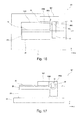
- Fig. 14 is a plan view showing a semiconductor laser module 401 according to a fifth embodiment of the present invention
- Fig. 15 is a front view of the semiconductor laser module 401.
- the semiconductor laser module 401 of the present embodiment has a lens fixture block 450 that is substantially in the form of a rectangular parallelepiped made of, for example, glass or the like.
- this lens fixture block 450 has a lens attachment surface 450A and a block fixation surface 450B, which are perpendicular to the X-direction and coplanar with each other.
- a groove 450C extending along the Y-direction is formed between the lens attachment surface 450A and the block fixation surface 450B of the lens fixture block 450.
- the collimator lens 40 has an end 40A along the X-direction that is fixed to the lens attachment surface 450A of the lens fixture block 450 with a lens fixation resin 42.
- the second substrate 20 has a side surface 20A along the X-direction that is fixed to the block fixation surface 450B of the lens fixture block 450 with a block fixation resin 52.
- the lens fixture block 450 is held out of contact with the first substrate 10. In other words, the lens fixture block 450 is cantilevered by the second substrate 20.
- a lens fixation resin 42 applied to the lens attachment surface 450A of the lens fixture block 450 exceeds a certain amount, an excess lens fixation resin 42 flows into the groove 450C between the lens attachment surface 450A and the block fixation surface 450B. Therefore, the lens fixation resin 42 is prevented from being brought into contact with the second substrate 20 when the lens fixture block 450 is brought closer to the semiconductor laser device 30.
- Fig. 16 is a plan view showing a semiconductor laser module 501 according to a sixth embodiment of the present invention
- Fig. 17 is a front view of the semiconductor laser module 501.
- the sixth embodiment is a combination of the aforementioned second embodiment and fifth embodiment.
- the semiconductor laser module 501 of the present embodiment has a device-mounting portion on which a semiconductor laser device 30 is mounted.
- the device-mounting portion includes a second substrate 20, which is a mounting substrate on which the semiconductor laser device 30 is mounted, and a third substrate 120 as a spacer.
- Such a spacer 120 allows the semiconductor laser device 30 to be located at a desired height.
- the semiconductor laser module 501 of the present embodiment has a lens fixture block 550 that is substantially in the form of a rectangular parallelepiped made of, for example, glass or the like.
- this lens fixture block 550 has a lens attachment surface 550A and a block fixation surface 550B, which are perpendicular to the X-direction and coplanar with each other.
- a groove 550C extending along the Y-direction is formed between the lens attachment surface 550A and the block fixation surface 550B of the lens fixture block 550.
- the collimator lens 40 has an end 40A along the X-direction that is fixed to the lens attachment surface 550A of the lens fixture block 550 with a lens fixation resin 42.
- the third substrate 120 has a side surface 120A along the X-direction that is fixed to the block fixation surface 550B of the lens fixture block 550 with a block fixation resin 52.
- the lens fixture block 550 is held out of contact with the first substrate 10. In other words, the lens fixture block 550 is cantilevered by the third substrate 120.
- the above embodiments describe a configuration of fixing only one of ends of the collimator lens 40 along the X-direction.
- a similar lens fixture block may be provided for another end of the collimator lens 40 so as to fix both of the ends of the collimator lens 40 along the X-direction.
- the collimator lens 40 in the above embodiments collimates components of the laser beam L along the direction of the fast axis (Y-direction).
- the present invention is also applicable to use of a lens for collimating components of the laser beam L along the direction of the slow axis (X-direction).
- the lens attachment surface and the block fixation surface of the lens fixture block is arranged in parallel to the XZ-plane, and an end of the collimator lens along the Y-direction is fixed to the lens attachment surface.
- the present invention is suitable for use in a semiconductor laser module including a semiconductor laser device and a collimator lens for collimating a laser beam emitted from the semiconductor laser device.
Landscapes
- Physics & Mathematics (AREA)
- General Physics & Mathematics (AREA)
- Optics & Photonics (AREA)
- Condensed Matter Physics & Semiconductors (AREA)
- Electromagnetism (AREA)
- Semiconductor Lasers (AREA)
- Optical Couplings Of Light Guides (AREA)
Abstract
Description
- The present invention relates to a semiconductor laser module and a method of manufacturing the same. More particularly, the present invention relates to a semiconductor laser module including a semiconductor laser device and a collimator lens for collimating a laser beam emitted from the semiconductor laser device and to a method of manufacturing such a semiconductor laser module.
- Generally, a direction perpendicular to a p-n junction of a semiconductor laser device is referred to as a fast axis, whereas a direction in parallel to the p-n junction is referred to as a slow axis. A numerical aperture of a semiconductor laser device in a direction along its fast axis is much greater than that in a direction along its slow axis. Therefore, a laser beam emitted from a semiconductor laser device greatly spreads in a direction along its fast axis. Accordingly, a collimator lens for collimating fast-axis components of a laser beam emitted from a semiconductor laser device should be arranged near an emitting surface of the semiconductor laser device (see, e.g.,
Patent Literature 1 and Patent Literature 2). - In order to arrange a desired optical system using such a collimator lens, it is necessary to fix the collimator lens highly precisely relative to a semiconductor laser device in a direction parallel to an optical axis and a direction parallel to a fast axis and to prevent variations in positional relationship between the semiconductor laser device and the collimator lens. Specifically, the positional relationship between the semiconductor laser device and the collimator lens should be fixed and maintained in the micron order.
- For example, in an optical fiber attachment apparatus disclosed in
Fig. 4 ofPatent Literature 1, a collimator lens (optical fiber lens 26) is attached so that it can slide along its axis. In order to attach the optical fiber lens 26 in a slidable manner, a certain clearance needs to be formed between acylindrical clamp 52 and the optical fiber lens 26. Therefore, variation in position of the optical fiber lens 26 cannot be reduced in the micron order in both of a direction of an optical axis of a laser beam emitted from a semiconductorlaser device bar 10 and a direction along a fast axis. - Furthermore, the optical fiber lens 26 of
Patent Literature 1 is fixed to anattachment member 40 with anepoxy resin 50. The optical fiber lens 26 is deviated in the direction of the optical axis of the laser beam by shrinkage of theepoxy resin 50 on curing. Moreover, since the optical fiber lens 26 is fixed directly to theattachment member 40 with theepoxy resin 50, the amount of theepoxy resin 50 that is not less than required for alignment needs to be provided between theattachment member 40 and the optical fiber lens 26 in order to conduct alignment of the optical fiber lens 26. The optical fiber lens 26 is also deviated in a direction along its fast axis by shrinkage or expansion of theepoxy resin 50 due to a temperature change or a humidity change. - Furthermore, Patent Literature 2 discloses a semiconductor laser module in which a
semiconductor laser device 1 and a collimator lens 6 are fixed to one supplementary member 4 with brazing layers 5 and 8, respectively, to reduce variations in positional relationship between thesemiconductor laser device 1 and the collimator lens 6 in cooperation with deflection of thesemiconductor laser device 1 and deflection of the collimator lens 6. When the position of thesemiconductor laser device 1 is adjusted, thesemiconductor laser device 1 needs to be positioned at a high temperature of, for example, about 400°C in order to braze the brazing layers 5 and 8. However, a laser beam cannot be emitted from thesemiconductor laser device 1 at such a high temperature. Thus, there is a problem that the collimator lens 6 cannot be aligned while a laser beam is emitted from the semiconductor laser device 1 (what is called active alignment cannot be performed). - In this case, active alignment can be performed if the
semiconductor laser device 1 and the collimator lens 6 are fixed with a resin or the like instead of the brazing layers 5 and 8. In such a case, however, the position of the supplementary member 4 and the collimator lens 6 greatly varies relative to thesemiconductor laser device 1 due to shrinkage or expansion of the resin. Accordingly, there is a problem that the collimator lens 6 is deviated from the aligned position. -
- Patent Literature 1:
JP 2004-200634 A - Patent Literature 2:
JP 3423723 B - The present invention has been made in view of the above drawbacks in the prior art. It is, therefore, a first object of the present invention to provide a semiconductor laser module capable of reducing influence from shrinkage or expansion of a resin for fixing a collimator lens and of holding the collimator lens in a highly precisely aligned state.
- Furthermore, a second object of the present invention is to provide a method of manufacturing a semiconductor laser module that can fix a collimator lens with high precision relative to a semiconductor laser device while active alignment of the collimator lens is performed.
- According to a first aspect of the present invention, there is provided a semiconductor laser module capable of reducing influence from shrinkage or expansion of a resin for fixing a collimator lens and of holding the collimator lens in a highly precisely aligned state. The semiconductor laser module has a substrate, a device-mounting portion provided on the substrate, and a semiconductor laser device mounted on the device-mounting portion. The semiconductor laser device emits a laser beam having an optical axis along a first direction. The semiconductor laser module has a collimator lens configured to collimate a component of the laser beam emitted from the semiconductor laser device along a second direction perpendicular to the first direction and a lens fixture block having a lens attachment surface perpendicular to a third direction that is perpendicular to the first direction and the second direction and a block fixation surface perpendicular to the third direction. At least one of ends of the collimator lens along the third direction is fixed to the lens attachment surface of the lens fixture block with a lens fixation resin. The block fixation surface of the lens fixture block is fixed to a side surface of the device-mounting portion along the third direction with a block fixation resin.
- Thus, according to the first aspect of the present invention, the lens fixation resin for fixing the collimator lens is provided between the end of the collimator lens along the third direction and the lens attachment surface perpendicular to the third direction. Therefore, shrinkage of the lens fixation resin on curing or shrinkage or expansion of the lens fixation resin due to a temperature change or a humidity change primarily causes the position of the collimator lens to vary only in the third direction. Furthermore, the position of the collimator lens does not need to be adjusted in the third direction. Thus, in terms of optics, the collimator lens may be located at any position in the third direction. Therefore, the thickness of the lens fixation resin between the collimator lens and the lens attachment surface can be reduced so as to reduce the amount of variation of the lens fixation resin per se due to shrinkage or expansion of the lens fixation resin. Accordingly, the collimator lens hardly changes its position in the first direction or the second direction. As a result, influence from shrinkage or expansion of the lens fixation resin for fixing the collimator lens can be reduced. Thus, the collimator lens can be held in a highly precisely aligned state.
- Furthermore, the block fixation resin for fixing the lens fixture block is provided between the block fixation surface of the lens fixture block, which is perpendicular to the third direction, and the side surface of the device-mounting portion along the third direction. Therefore, shrinkage or expansion of the block fixation resin primarily causes the position of the lens fixture block to vary only in the third direction. Furthermore, the position of the collimator lens does not need to be adjusted in the third direction. Thus, in terms of optics, the collimator lens may be located at any position in the third direction. Therefore, the thickness of the block fixation resin between the lens fixture block and the side surface of the device-mounting portion along the third direction can be reduced so as to reduce the amount of variation of the block fixation resin per se due to shrinkage or expansion of the block fixation resin. Accordingly, the lens fixture block hardly changes its position in the Y-direction or the Z-direction. As a result, the collimator lens, which is fixed to the lens fixture block, hardly changes its position in the Y-direction or the Z-direction. Thus, the collimator lens can be held in a highly precisely aligned state.
- The second direction may be a direction along a fast axis of the laser beam emitted from the semiconductor laser device. Furthermore, a UV-curable resin or a thermosetting resin may be used as the lens fixation resin. Moreover, a UV-curable resin or a thermosetting resin may be used as the block fixation resin. The device-mounting portion may include a mounting substrate on which the semiconductor laser device is mounted and a spacer having a certain thickness. The block fixation surface of the lens fixture block may be fixed to a side surface of the spacer of the device-mounting portion along the third direction with the block fixation resin.
- Preferably, an equal amount of the lens fixation resin is present on opposite sides of the collimator lens along the first direction. With this configuration, the lens fixation resin equally shrinks or expands on the opposite sides of the collimator lens along the first direction so that the shrinkage or expansion is cancelled out on the opposite sides of the collimator lens along the first direction. Accordingly, shrinkage or expansion of the lens fixation resin exerts substantially no influence on the collimator lens along the first direction. Similarly, an equal amount of the lens fixation resin is preferably present on opposite sides of the collimator lens along the second direction. With this configuration, the lens fixation resin equally shrinks or expands on the opposite sides of the collimator lens along the second direction so that the shrinkage or expansion is cancelled out on the opposite sides of the collimator lens along the second direction. Accordingly, shrinkage or expansion of the lens fixation resin exerts substantially no influence on the collimator lens along the second direction.
- The position of the lens attachment surface of the lens fixture block may be located farther away from the device-mounting portion than the position of the block fixation surface of the lens fixture block along the third direction. Alternatively, a groove may be formed between the lens attachment surface and the block fixation surface of the lens fixture block for preventing the lens fixation resin from being brought into contact with the device-mounting portion. With those configurations, the lens fixation resin is prevented from being brought into contact with the device-mounting portion when the lens fixture block is brought closer to the device-mounting portion.
- According to a second aspect of the present invention, there is provided a method of manufacturing a semiconductor laser module that can fix a collimator lens with high precision relative to a semiconductor laser device while active alignment of the collimator lens is performed. This manufacturing method produces a semiconductor laser module having a semiconductor laser device operable to emit a laser beam having an optical axis along a first direction and a collimator lens configured to collimate a component of the laser beam emitted from the semiconductor laser device along a second direction perpendicular to the first direction. With this manufacturing method, the semiconductor laser device is mounted to a device-mounting portion, and the device-mounting portion is fixed to a substrate. A lens fixation resin is applied to a lens attachment surface formed on a lens fixture block. An end of the collimator lens along the third direction is inserted into the lens fixation resin applied to the lens attachment surface in a state in which the lens attachment surface is perpendicular to a third direction that is perpendicular to the first direction and the second direction. The lens fixation resin is hardened to fix the collimator lens to the lens fixture block. Furthermore, a block fixation resin is applied to a side surface of the device-mounting portion along the third direction. The lens fixture block is brought into contact with the block fixation resin. The collimator lens is positioned into a desired location while a laser beam is emitted from the semiconductor laser device. When the collimator lens has been positioned, the block fixation resin is hardened to fix the lens fixture block and the collimator lens relative to the device-mounting portion.
- Thus, according to the second aspect of the present invention, the collimator lens is fixed to the lens fixture block with the lens fixation resin. Therefore, this method does not require to hold an atmosphere at a high temperature, unlike solder jointing disclosed in Patent Literature 2. Accordingly, the collimator lens can be positioned in place while a laser beam is emitted from the semiconductor laser device (active alignment). Additionally, the lens fixation resin is provided between the end of the collimator lens along the third direction and the lens attachment surface parallel to the laser beam (first direction). Therefore, shrinkage of the lens fixation resin on curing or shrinkage or expansion of the lens fixation resin due to a temperature change or a humidity change primarily causes the position of the collimator lens to vary only in the third direction. Furthermore, the position of the collimator lens does not need to be adjusted in the third direction. Thus, in terms of optics, the collimator lens may be located at any position in the third direction. Therefore, the thickness of the lens fixation resin between the collimator lens and the lens attachment surface can be reduced so as to reduce the amount of variation of the lens fixation resin per se due to shrinkage or expansion of the lens fixation resin. Accordingly, the collimator lens hardly changes its position in the first direction or the second direction. As a result, the collimator lens can be fixed to the semiconductor laser device with high precision.
- Furthermore, the block fixation resin for fixing the lens fixture block is provided between the block fixation surface of the lens fixture block, which is perpendicular to the third direction, and the side surface of the device-mounting portion along the third direction. Therefore, shrinkage or expansion of the block fixation resin primarily causes the position of the lens fixture block to vary only in the third direction. Furthermore, the position of the collimator lens does not need to be adjusted in the third direction. Thus, in terms of optics, the collimator lens may be located at any position in the third direction. Therefore, the thickness of the block fixation resin between the lens fixture block and the side surface of the device-mounting portion along the third direction can be reduced so as to reduce the amount of variation of the block fixation resin per se due to shrinkage or expansion of the block fixation resin. Accordingly, the lens fixture block hardly changes its position in the Y-direction or the Z-direction. As a result, the collimator lens, which is fixed to the lens fixture block, hardly changes its position in the Y-direction or the Z-direction. Thus, the collimator lens can be held in a highly precisely aligned state.
- The second direction may be a direction along a fast axis of the laser beam emitted from the semiconductor laser device. Furthermore, a UV-curable resin or a thermosetting resin may be used as the lens fixation resin. Moreover, a UV-curable resin or a thermosetting resin may be used as the block fixation resin. The device-mounting portion may include a mounting substrate and a spacer having a certain thickness. The semiconductor laser device may be mounted on the mounting substrate, and the mounting substrate may be fixed to the spacer. The block fixation surface of the lens fixture block may be fixed to a side surface of the spacer of the device-mounting portion along the third direction with the block fixation resin. The block fixation resin may be applied to a side surface of the spacer along the third direction.
- Furthermore, when the end of the collimator lens is inserted into the lens fixation resin, it is preferable to equalize the amounts of the lens fixation resin present on opposite sides of the collimator lens along the first direction. With this configuration, the lens fixation resin equally shrinks or expands on the opposite sides of the collimator lens along the first direction so that the shrinkage or expansion is cancelled out on the opposite sides of the collimator lens along the first direction. Accordingly, shrinkage or expansion of the lens fixation resin exerts substantially no influence on the collimator lens along the first direction. Similarly, it is preferable to equalize the amounts of the lens fixation resin present on opposite side of the collimator lens along the second direction. With this configuration, the lens fixation resin equally shrinks or expands on the opposite sides of the collimator lens along the second direction so that the shrinkage or expansion is cancelled out on the opposite sides of the collimator lens along the second direction. Accordingly, shrinkage or expansion of the lens fixation resin exerts substantially no influence on the collimator lens along the second direction.
- According to the present invention, there can be provided a semiconductor laser module capable of reducing influence from shrinkage or expansion of a resin for fixing a collimator lens and of holding the collimator lens in a highly precisely aligned state. Furthermore, according to the present invention, there can be provided a method of manufacturing a semiconductor laser module that can fix a collimator lens with high precision relative to a semiconductor laser device while active alignment of the collimator lens is performed.
-
- [
Fig. 1] Fig. 1 is a plan view showing a semiconductor laser module according to a first embodiment of the present invention. - [
Fig. 2] Fig. 2 is a front view of the semiconductor laser module shown inFig. 1 . - [
Fig. 3] Fig. 3 is a side view of the semiconductor laser module shown inFig. 1 . - [
Fig. 4] Fig. 4 is a diagram explanatory of a method of manufacturing the semiconductor laser module shown inFig. 1 . - [
Fig. 5] Fig. 5 is a diagram explanatory of a method of manufacturing the semiconductor laser module shown inFig. 1 . - [
Fig. 6] Fig. 6 is a diagram explanatory of a method of manufacturing the semiconductor laser module shown inFig. 1 . - [
Fig. 7] Fig. 7 is a plan view showing a semiconductor laser module according to a second embodiment of the present invention. - [
Fig. 8] Fig. 8 is a front view of the semiconductor laser module shown inFig. 7 . - [
Fig. 9] Fig. 9 is a side view of the semiconductor laser module shown inFig. 7 . - [
Fig. 10] Fig. 10 is a plan view showing a semiconductor laser module according to a third embodiment of the present invention. - [
Fig. 11] Fig. 11 is a front view of the semiconductor laser module shown inFig. 10 . - [
Fig. 12] Fig. 12 is a plan view showing a semiconductor laser module according to a fourth embodiment of the present invention. - [
Fig. 13] Fig. 13 is a front view of the semiconductor laser module shown inFig. 12 . - [
Fig. 14] Fig. 14 is a plan view showing a semiconductor laser module according to a fifth embodiment of the present invention. - [
Fig. 15] Fig. 15 is a front view of the semiconductor laser module shown inFig. 14 . - [
Fig. 16] Fig. 16 is a plan view showing a semiconductor laser module according to a sixth embodiment of the present invention. - [
Fig. 17] Fig. 17 is a front view of the semiconductor laser module shown inFig. 16 . - Embodiments of a semiconductor laser module according to the present invention will be described in detail below with reference to
Figs. 1 to 8 . The same or corresponding components are denoted by the same reference numerals inFigs. 1 to 8 so as to avoid redundant explanation. -
Fig. 1 is a plan view showing asemiconductor laser module 1 according to a first embodiment of the present invention,Fig. 2 is a front view thereof, andFig. 3 is a side view thereof. As shown inFigs. 1 to 3 , thesemiconductor laser module 1 of this embodiment has afirst substrate 10, a second substrate 20 (device-mounting portion) fixed onto thefirst substrate 10, a semiconductor laser device (laser diode) 30 mounted on thesecond substrate 20, and acollimator lens 40 for collimating a laser beam emitted from thesemiconductor laser device 30. InFig. 1 , thesemiconductor laser device 30 emits a laser beam L along the Z-direction. The following description assumes that the Y-direction illustrated inFig. 2 is parallel to a fast axis of the laser beam L. - The
collimator lens 40 collimates components of the laser beam L emitted from thesemiconductor laser device 30 along a direction of the fast axis (Y-direction) to generate parallel rays. In the present embodiment, as shown in a cross-section of thecollimator lens 40 on the YZ-plane inFig. 2 , a surface of thecollimator lens 40 into which the laser beam L is incident is in parallel to the Y-axis, and a surface of thecollimator lens 40 from which the laser beam is outputted is convex. With such a cross-section, thecollimator lens 40 extends along a direction of the slow axis of the laser beam L (X-direction). For example, thecollimator lens 40 has a length of about 2 mm along the X-direction. Thecollimator lens 40 is aligned to generate desired parallel rays and positioned highly precisely with respect to the Y-direction and the Z-direction. - As shown in
Figs. 1 to 3 , thesemiconductor laser module 1 of the present embodiment has alens fixture block 50 that is substantially in the form of a rectangular parallelepiped made of, for example, glass or the like. Thelens fixture block 50 has alens attachment surface 50A and ablock fixation surface 50B, which are in parallel to an optical axis of the laser beam L. In the present embodiment, thelens attachment surface 50A and theblock fixation surface 50B are coplanar with each other. Thelens attachment surface 50A and theblock fixation surface 50B are also configured to be in parallel to the fast axis (Y-direction) of the laser beam L, i.e., to be perpendicular to the X-direction. - As shown in
Figs. 1 and3 , theblock fixation surface 50B of thelens fixture block 50 is fixed to aside surface 20A of thesecond substrate 20 in the X-direction with ablock fixation resin 52. Thelens fixture block 50 is held out of contact with thefirst substrate 10. In other words, thelens fixture block 50 is cantilevered by thesecond substrate 20. For example, UV-curable resins or thermosetting resins may be used as theblock fixation resin 52. Here, it is preferable to reduce the thickness of theblock fixation resin 52 between theblock fixation surface 50B of thelens fixture block 50 and theside surface 20A of thesecond substrate 20. - The
collimator lens 40 has anend 40A along the X-direction that is fixed to thelens attachment surface 50A of thelens fixture block 50 with alens fixation resin 42. Thecollimator lens 40 is held out of contact with thefirst substrate 10. In other words, thecollimator lens 40 is cantilevered by thelens fixture block 50. For example, UV-curable resins or thermosetting resins may be used as thelens fixation resin 42. Thelens fixation resin 42 fixes theend 40A of thecollimator lens 40 in the X-direction, the Y-direction, and the Z-direction. Preferably, an equal amount of thelens fixation resin 42 is present on opposite sides of thecollimator lens 40 along the Z-direction. Furthermore, an equal amount of thelens fixation resin 42 is preferably present on opposite sides of thecollimator lens 40 along the Y-direction. Moreover, it is preferable to reduce the thickness of thelens fixation resin 42 between thecollimator lens 40 and thelens attachment surface 50A. - The
lens fixation resin 42 for fixing thecollimator lens 40 is provided between theend 40A of thecollimator lens 40 along the X-direction and thelens attachment surface 50A, which is perpendicular to the X-direction. Therefore, shrinkage of thelens fixation resin 42 on curing or shrinkage or expansion of thelens fixation resin 42 due to a temperature change or a humidity change primarily causes the position of thecollimator lens 40 to vary only in the X-direction, i.e., the direction of the slow axis. Furthermore, reduction in thickness of thelens fixation resin 42 between thecollimator lens 40 and thelens attachment surface 50A can reduce the amount of variation of thelens fixation resin 42 per se due to shrinkage or expansion of thelens fixation resin 42. Therefore, thecollimator lens 40 hardly changes its position in the Y-direction or the Z-direction. Accordingly, thecollimator lens 40 can be held in a highly precisely aligned state. - In the example shown in
Figs. 1 to 3 , the entire end surface of theend 40A of thecollimator lens 40 along the X-direction is fixed to thelens attachment surface 50A with thelens fixation resin 42. Nevertheless, at least part of the end surface of theend 40A of thecollimator lens 40 along the X-direction may be fixed to thelens attachment surface 50A with thelens fixation resin 42. - Furthermore, when an equal amount of the
lens fixation resin 42 is present on opposite sides of thecollimator lens 40 along the Z-direction, thelens fixation resin 42 equally shrinks or expands on the opposite sides of thecollimator lens 40 so that the shrinkage or expansion is cancelled out on the opposite sides of thecollimator lens 40. Accordingly, shrinkage or expansion of thelens fixation resin 42 exerts substantially no influence on thecollimator lens 40 along the Z-direction. Moreover, when an equal amount of thelens fixation resin 42 is present on opposite sides of thecollimator lens 40 along the Y-direction, thelens fixation resin 42 equally shrinks or expands on the opposite sides of thecollimator lens 40 so that the shrinkage or expansion is cancelled out on the opposite sides of thecollimator lens 40. Accordingly, shrinkage or expansion of thelens fixation resin 42 exerts substantially no influence on thecollimator lens 40 along the Y-direction. - Furthermore, the
block fixation resin 52 for fixing thelens fixture block 50 is provided between theblock fixation surface 50B of thelens fixture block 50, which is perpendicular to the X-direction, and theside surface 20A of thesecond substrate 20 along the X-direction. Therefore, shrinkage or expansion of theblock fixation resin 52 primarily causes the position of thelens fixture block 50 to vary only in the X-direction. Furthermore, reduction in thickness of theblock fixation resin 52 between theblock fixation surface 50B of thelens fixture block 50 and theside surface 20A of thesecond substrate 20 can reduce the amount of variation of thelens fixation resin 42 per se due to shrinkage or expansion of thelens fixation resin 42. Therefore, thelens fixture block 50 hardly changes its position in the Y-direction or the Z-direction. Accordingly, thecollimator lens 40, which is fixed to thelens fixture block 50, hardly changes its position in the Y-direction or the Z-direction. Thus, thecollimator lens 40 can be held in a highly precisely aligned state. - Now a method of manufacturing a
semiconductor laser module 1 according to the present invention will be described. When asemiconductor laser module 1 is to be manufactured, asemiconductor laser device 30 is first mounted onto asecond substrate 20 as a device-mounting portion. Then thesecond substrate 20 having thesemiconductor laser device 30 mounted thereon is fixed onto a first substrate 10 (Fig. 4 ). - Furthermore, a
lens fixation resin 42 is applied to thelens attachment surface 50A of thelens fixture block 50. Anend 40A of acollimator lens 40 is inserted into thelens fixation resin 42 in a direction perpendicular to thelens attachment surface 50A (Fig. 5 ). Then thelens fixation resin 42 is hardened to fix thecollimator lens 40 to thelens fixture block 50. At that time, it is preferable to minimize the thickness of thelens fixation resin 42 between thecollimator lens 40 and thelens attachment surface 50A. - Next, a
block fixation resin 52 is applied to aside surface 20A of thesecond substrate 20. Then thelens fixture block 50 to which thecollimator lens 40 has been fixed is brought into contact with a portion of thesecond substrate 20 to which theblock fixation resin 52 has been applied (Fig. 6 ). At that time, thelens fixture block 50 has alens attachment surface 50A that is perpendicular to the X-direction. - Subsequently, a laser beam is emitted from the
semiconductor laser device 30. In that state, thelens fixture block 50 is moved so that thecollimator lens 40 is positioned in place (active alignment). At that time, it is preferable to minimize the thickness of theblock fixation resin 52 between theblock fixation surface 50B of thelens fixture block 50 and theside surface 20A of thesecond substrate 20. While thecollimator lens 40 has been positioned in place with high precision, theblock fixation resin 52 is hardened to fix thelens fixture block 50 to thesecond substrate 20. In this manner, asemiconductor laser module 1 is completed (Fig. 1 ). - As described above, according to a method of manufacturing a
semiconductor laser module 1 in the present embodiment, thecollimator lens 40 is fixed to thelens fixture block 50 with thelens fixation resin 42. Therefore, this method does not require to hold an atmosphere at a high temperature, unlike solder jointing disclosed in Patent Literature 2. Accordingly, thecollimator lens 40 can be positioned in place while a laser beam is emitted from the semiconductor laser device 30 (active alignment). - Furthermore, the
end 40A of thecollimator lens 40 along the X-direction is fixed to thelens attachment surface 50A of thelens fixture block 50, which is perpendicular to the X-direction. Therefore, shrinkage of thelens fixation resin 42 on curing or shrinkage or expansion of thelens fixation resin 42 due to a temperature change or a humidity change hardly causes thecollimator lens 40 to change its position in the Y-direction or the Z-direction. Additionally, reduction in thickness of thelens fixation resin 42 between thecollimator lens 40 and thelens attachment surface 50A can reduce the amount of variation of thelens fixation resin 42 per se due to shrinkage or expansion of thelens fixation resin 42. Accordingly, thecollimator lens 40 can be held in a highly precisely aligned state. - Furthermore, the
block fixation surface 50B of thelens fixture block 50, which is perpendicular to the X-direction, is fixed to theside surface 20A of thesecond substrate 20 along the X-direction. Therefore, shrinkage of theblock fixation resin 52 on curing or shrinkage or expansion of theblock fixation resin 52 due to a temperature change or a humidity change hardly causes thelens fixture block 50 to change its position in the Y-direction or the Z-direction. Additionally, reduction in thickness of theblock fixation resin 52 between theblock fixation surface 50B of thelens fixture block 50 and theside surface 20A of thesecond substrate 20 can reduce the amount of variation of theblock fixation resin 52 per se due to shrinkage or expansion of theblock fixation resin 52. Accordingly, thecollimator lens 40, which is fixed to thelens fixture block 50, hardly changes its position in the Y-direction or the Z-direction. As a result, thecollimator lens 40 can be held in a highly precisely aligned state. -
Fig. 7 is a plan view showing asemiconductor laser module 101 according to a second embodiment of the present invention,Fig. 8 is a front view of thesemiconductor laser module 101, andFig. 9 is a side view of thesemiconductor laser module 101. As shown inFigs. 7 to 9 , thesemiconductor laser module 101 of the present embodiment has a device-mounting portion on which asemiconductor laser device 30 is mounted. The device-mounting portion includes asecond substrate 20, which is a mounting substrate on which thesemiconductor laser device 30 is mounted, and athird substrate 120 as a spacer. Such aspacer 120 allows thesemiconductor laser device 30 to be located at a desired height. - Furthermore, the
semiconductor laser module 101 of the present embodiment has alens fixture block 150 that is substantially in the form of a rectangular parallelepiped made of, for example, glass or the like. Thislens fixture block 150 has alens attachment surface 150A and ablock fixation surface 150B, which are perpendicular to the X-direction and coplanar with each other. Thecollimator lens 40 has anend 40A along the X-direction that is fixed to thelens attachment surface 150A with alens fixation resin 42. - As shown in
Figs. 7 and9 , thethird substrate 120 has aside surface 120A along the X-direction that is fixed to theblock fixation surface 150B of thelens fixture block 150 with ablock fixation resin 52. Thelens fixture block 150 is held out of contact with thefirst substrate 10. In other words, thelens fixture block 150 is cantilevered by thethird substrate 120. - Generally, a substrate on which the
semiconductor laser device 30 is mounted often has a thickness of less than 0.5 mm along the fast axis direction (Y-direction). Therefore, in the aforementioned first embodiment, the width of theblock fixation surface 50B of thelens fixture block 50 along the Y-direction is very small. In the present embodiment, since thespacer 120 having an appropriate thickness is provided between thefirst substrate 10 and thesecond substrate 20 so that thelens fixture block 150 is fixed to thespacer 120, a sufficient area can be ensured in theblock fixation surface 150B. Thus, thespacer 120 preferably has a thickness of 0.3 mm or more along the Y-direction. -
Fig. 10 is a plan view showing asemiconductor laser module 201 according to a third embodiment of the present invention, andFig. 11 is a front view of thesemiconductor laser module 201. As shown inFigs. 10 and 11 , thesemiconductor laser module 201 of the present embodiment has alens fixture block 250 that is substantially in the form of a rectangular parallelepiped made of, for example, glass or the like. As with the first embodiment, thelens fixture block 250 has alens attachment surface 250A and ablock fixation surface 250B, which are perpendicular to the X-direction. As shown inFig. 10 , however, the position of thelens attachment surface 250A of thelens fixture block 250 is deviated from the position of theblock fixation surface 250B along the X-direction. Therefore, thelens attachment surface 250A and theblock fixation surface 250B form astep 250C. - The
collimator lens 40 has anend 40A along the X-direction that is fixed to thelens attachment surface 250A of thelens fixture block 250 with alens fixation resin 42. Thesecond substrate 20 has aside surface 20A along the X-direction that is fixed to theblock fixation surface 250B of thelens fixture block 250 with ablock fixation resin 52. Thelens fixture block 250 is held out of contact with thefirst substrate 10. In other words, thelens fixture block 250 is cantilevered by thesecond substrate 20. - Since a laser beam L emitted from the
semiconductor laser device 30 spreads in the direction of the fast axis as described above, it is preferable to arrange thecollimator lens 40 closer to an emitting surface of thesemiconductor laser device 30. However, if thecollimator lens 40 is arranged excessively close to the emitting surface of thesemiconductor laser device 30 in the aforementioned first embodiment, thelens fixation resin 42 for fixing thecollimator lens 40 may be brought into contact with thesecond substrate 20. If thelens fixation resin 42 is brought into contact with thesecond substrate 20, thecollimator lens 40 is also fixed to an edge of thesecond substrate 20 along the Z-direction via thelens fixation resin 42. Therefore, shrinkage or expansion of thelens fixation resin 42 causes changes in position of thecollimator lens 40 along the Z-direction. In the present embodiment, thelens attachment surface 250A of thelens fixture block 250 is arranged farther away from thesecond substrate 20 than theblock fixation surface 250B along the X-direction so as to form thestep 250C. Thus, thelens fixation resin 42 is prevented from being brought into contact with thesecond substrate 20 when thelens fixture block 250 is brought closer to thesemiconductor laser device 30. -
Fig. 12 is a plan view showing asemiconductor laser module 301 according to a fourth embodiment of the present invention, andFig. 13 is a front view of thesemiconductor laser module 301. The fourth embodiment is a combination of the aforementioned second embodiment and third embodiment. Specifically, as shown inFigs. 12 and 13 , thesemiconductor laser module 301 of the present embodiment has a device-mounting portion on which asemiconductor laser device 30 is mounted. The device-mounting portion includes asecond substrate 20, which is a mounting substrate on which thesemiconductor laser device 30 is mounted, and athird substrate 120 as a spacer. Such aspacer 120 allows thesemiconductor laser device 30 to be located at a desired height. - Furthermore, the
semiconductor laser module 101 of the present embodiment has alens fixture block 350 that is substantially in the form of a rectangular parallelepiped made of, for example, glass or the like. As with the second embodiment, thislens fixture block 350 has alens attachment surface 350A and ablock fixation surface 350B, which are perpendicular to the X-direction. As shown inFig. 12 , however, thelens attachment surface 350A of thelens fixture block 350 is arranged farther away from thethird substrate 120 than theblock fixation surface 350B along the X-direction so as to form astep 350C. With this configuration, thelens fixation resin 42 is prevented from being brought into contact with thethird substrate 120 when thelens fixture block 350 is brought closer to thesemiconductor laser device 30. - The
collimator lens 40 has anend 40A along the X-direction that is fixed to thelens attachment surface 350A of thelens fixture block 350 with alens fixation resin 42. Thethird substrate 120 has aside surface 20A along the X-direction that is fixed to theblock fixation surface 350B of thelens fixture block 350 with ablock fixation resin 52. Thelens fixture block 350 is held out of contact with thefirst substrate 10. In other words, thelens fixture block 350 is cantilevered by thethird substrate 120. -
Fig. 14 is a plan view showing asemiconductor laser module 401 according to a fifth embodiment of the present invention, andFig. 15 is a front view of thesemiconductor laser module 401. As shown inFigs. 14 and 15 , thesemiconductor laser module 401 of the present embodiment has alens fixture block 450 that is substantially in the form of a rectangular parallelepiped made of, for example, glass or the like. As with the first embodiment, thislens fixture block 450 has alens attachment surface 450A and ablock fixation surface 450B, which are perpendicular to the X-direction and coplanar with each other. As shown inFig. 14 , however, agroove 450C extending along the Y-direction is formed between thelens attachment surface 450A and theblock fixation surface 450B of thelens fixture block 450. - The
collimator lens 40 has anend 40A along the X-direction that is fixed to thelens attachment surface 450A of thelens fixture block 450 with alens fixation resin 42. Thesecond substrate 20 has aside surface 20A along the X-direction that is fixed to theblock fixation surface 450B of thelens fixture block 450 with ablock fixation resin 52. Thelens fixture block 450 is held out of contact with thefirst substrate 10. In other words, thelens fixture block 450 is cantilevered by thesecond substrate 20. - In the present embodiment, if a
lens fixation resin 42 applied to thelens attachment surface 450A of thelens fixture block 450 exceeds a certain amount, an excesslens fixation resin 42 flows into thegroove 450C between thelens attachment surface 450A and theblock fixation surface 450B. Therefore, thelens fixation resin 42 is prevented from being brought into contact with thesecond substrate 20 when thelens fixture block 450 is brought closer to thesemiconductor laser device 30. -
Fig. 16 is a plan view showing asemiconductor laser module 501 according to a sixth embodiment of the present invention, andFig. 17 is a front view of thesemiconductor laser module 501. The sixth embodiment is a combination of the aforementioned second embodiment and fifth embodiment. Specifically, as shown inFigs. 16 and 17 , thesemiconductor laser module 501 of the present embodiment has a device-mounting portion on which asemiconductor laser device 30 is mounted. The device-mounting portion includes asecond substrate 20, which is a mounting substrate on which thesemiconductor laser device 30 is mounted, and athird substrate 120 as a spacer. Such aspacer 120 allows thesemiconductor laser device 30 to be located at a desired height. - Furthermore, the
semiconductor laser module 501 of the present embodiment has alens fixture block 550 that is substantially in the form of a rectangular parallelepiped made of, for example, glass or the like. As with the first embodiment, thislens fixture block 550 has alens attachment surface 550A and ablock fixation surface 550B, which are perpendicular to the X-direction and coplanar with each other. As shown inFig. 16 , however, a groove 550C extending along the Y-direction is formed between thelens attachment surface 550A and theblock fixation surface 550B of thelens fixture block 550. With this configuration, thelens fixation resin 42 is prevented from being brought into contact with thethird substrate 120 when thelens fixture block 550 is brought closer to thesemiconductor laser device 30. - The
collimator lens 40 has anend 40A along the X-direction that is fixed to thelens attachment surface 550A of thelens fixture block 550 with alens fixation resin 42. Thethird substrate 120 has aside surface 120A along the X-direction that is fixed to theblock fixation surface 550B of thelens fixture block 550 with ablock fixation resin 52. Thelens fixture block 550 is held out of contact with thefirst substrate 10. In other words, thelens fixture block 550 is cantilevered by thethird substrate 120. - The above embodiments describe a configuration of fixing only one of ends of the
collimator lens 40 along the X-direction. However, a similar lens fixture block may be provided for another end of thecollimator lens 40 so as to fix both of the ends of thecollimator lens 40 along the X-direction. - Moreover, the
collimator lens 40 in the above embodiments collimates components of the laser beam L along the direction of the fast axis (Y-direction). The present invention is also applicable to use of a lens for collimating components of the laser beam L along the direction of the slow axis (X-direction). In such a case, the lens attachment surface and the block fixation surface of the lens fixture block is arranged in parallel to the XZ-plane, and an end of the collimator lens along the Y-direction is fixed to the lens attachment surface. - Although some preferred embodiments of the present invention have been described, the present invention is not limited to the aforementioned embodiments. It should be understood that various different forms may be applied to the present invention within the technical idea thereof.
- The present invention is suitable for use in a semiconductor laser module including a semiconductor laser device and a collimator lens for collimating a laser beam emitted from the semiconductor laser device.
-
- L
- laser beam
- 1
- semiconductor laser module
- 10
- first substrate
- 20
- second substrate (mounting substrate)
- 20A
- side surface
- 30
- semiconductor laser device
- 40
- collimator lens
- 40A
- end
- 42
- lens fixation resin
- 50
- lens fixture block
- 50A
- lens attachment surface
- 50B
- block fixation surface
- 52
- block fixation resin
- 101
- semiconductor laser module
- 120
- third substrate (spacer)
- 120A
- side surface
- 150A
- lens attachment surface
- 150B
- block fixation surface
- 201
- semiconductor laser module
- 250A
- lens attachment surface
- 250B
- block fixation surface
- 250C
- step
- 301
- semiconductor laser module
- 350A
- lens attachment surface
- 350B
- block fixation surface
- 350C
- step
- 401
- semiconductor laser module
- 450A
- lens attachment surface
- 450B
- block fixation surface
- 450C
- groove
- 501
- semiconductor laser module
- 550A
- lens attachment surface
- 550B
- block fixation surface
- 550C
- groove
Claims (12)
- A semiconductor laser module characterized by comprising:a substrate;a device-mounting portion provided on the substrate;a semiconductor laser device mounted on the device-mounting portion, the semiconductor laser device emitting a laser beam having an optical axis along a first direction;a collimator lens configured to collimate a component of the laser beam emitted from the semiconductor laser device along a second direction perpendicular to the first direction; anda lens fixture block having a lens attachment surface perpendicular to a third direction that is perpendicular to the first direction and the second direction and a block fixation surface perpendicular to the third direction,wherein at least one of ends of the collimator lens along the third direction is fixed to the lens attachment surface of the lens fixture block with a lens fixation resin, andthe block fixation surface of the lens fixture block is fixed to a side surface of the device-mounting portion along the third direction with a block fixation resin.
- The semiconductor laser module as recited in claim 1, characterized in that the second direction is a direction along a fast axis of the laser beam emitted from the semiconductor laser device.
- The semiconductor laser module as recited in claim 1 or 2, characterized in that a position of the lens attachment surface of the lens fixture block is located farther away from the device-mounting portion than a position of the block fixation surface of the lens fixture block along the third direction.
- The semiconductor laser module as recited in claim 1 or 2, characterized in that a groove is formed between the lens attachment surface and the block fixation surface of the lens fixture block for preventing the lens fixation resin from being brought into contact with the device-mounting portion.
- The semiconductor laser module as recited in any one of claims 1 to 4, characterized in that the device-mounting portion includes a mounting substrate on which the semiconductor laser device is mounted and a spacer having a certain thickness,
wherein the block fixation surface of the lens fixture block is fixed to a side surface of the spacer of the device-mounting portion along the third direction with the block fixation resin. - The semiconductor laser module as recited in any one of claims 1 to 5, characterized in that the lens fixation resin is a UV-curable resin or a thermosetting resin.
- The semiconductor laser module as recited in any one of claims 1 to 6, characterized in that the block fixation resin is a UV-curable resin or a thermosetting resin.
- The semiconductor laser module as recited in any one of claims I to 7, characterized in that an equal amount of the lens fixation resin is present on opposite sides of the collimator lens along the first direction, and
an equal amount of lens fixation resin is present on opposite side of the collimator lens along the second direction. - A method of manufacturing a semiconductor laser module having a semiconductor laser device operable to emit a laser beam having an optical axis along a first direction and a collimator lens configured to collimate a component of the laser beam emitted from the semiconductor laser device along a second direction perpendicular to the first direction, characterized by:mounting the semiconductor laser device to a device-mounting portion;fixing the device-mounting portion to a substrate;applying a lens fixation resin to a lens attachment surface formed on a lens fixture block;inserting an end of the collimator lens along the third direction into the lens fixation resin applied to the lens attachment surface in a state in which the lens attachment surface is perpendicular to a third direction that is perpendicular to the first direction and the second direction;hardening the lens fixation resin to fix the collimator lens to the lens fixture block;applying a block fixation resin to a side surface of the device-mounting portion along the third direction;bringing the lens fixture block into contact with the block fixation resin;positioning the collimator lens into a desired location while emitting a laser beam from the semiconductor laser device; andwhen the collimator lens has been positioned, hardening the block fixation resin to fix the lens fixture block and the collimator lens relative to the device-mounting portion.
- The method of manufacturing a semiconductor laser module as recited in claim 9, characterized in that the second direction is a direction along a fast axis of the laser beam emitted from the semiconductor laser device.
- The method of manufacturing a semiconductor laser module as recited in claim 9 or 10, characterized in that the inserting the end of the collimator lens into the lens fixation resin comprises equalizing amounts of the lens fixation resin present on opposite sides of the collimator lens along the first direction and equalizing amounts of the lens fixation resin present on opposite side of the collimator lens along the second direction.
- The method of manufacturing a semiconductor laser module as recited in any one of claims 9 to 11, characterized in that the device-mounting portion includes a mounting substrate and a spacer having a certain thickness,
wherein the mounting the semiconductor laser device to the device-mounting portion comprises:mounting the semiconductor laser device to the mounting substrate, andfixing the mounting substrate to the spacer,wherein the applying the block fixation resin to the side surface of the device-mounting portion along the third direction comprises applying the block fixation resin to a side surface of the spacer along the third direction.
Applications Claiming Priority (2)
| Application Number | Priority Date | Filing Date | Title |
|---|---|---|---|
| JP2013043015A JP5616471B2 (en) | 2013-03-05 | 2013-03-05 | Semiconductor laser module and manufacturing method thereof |
| PCT/JP2014/055239 WO2014136709A1 (en) | 2013-03-05 | 2014-03-03 | Semiconductor laser module and production method for same |
Publications (2)
| Publication Number | Publication Date |
|---|---|
| EP2966736A1 true EP2966736A1 (en) | 2016-01-13 |
| EP2966736A4 EP2966736A4 (en) | 2016-11-02 |
Family
ID=51491227
Family Applications (1)
| Application Number | Title | Priority Date | Filing Date |
|---|---|---|---|
| EP14759748.8A Withdrawn EP2966736A4 (en) | 2013-03-05 | 2014-03-03 | Semiconductor laser module and production method for same |
Country Status (5)
| Country | Link |
|---|---|
| US (1) | US9647421B2 (en) |
| EP (1) | EP2966736A4 (en) |
| JP (1) | JP5616471B2 (en) |
| CN (1) | CN105027368A (en) |
| WO (1) | WO2014136709A1 (en) |
Families Citing this family (15)
| Publication number | Priority date | Publication date | Assignee | Title |
|---|---|---|---|---|
| CN106797102B (en) * | 2014-10-22 | 2020-04-21 | 松下知识产权经营株式会社 | Laser module |
| JP6140670B2 (en) * | 2014-11-17 | 2017-05-31 | 株式会社フジクラ | Semiconductor laser device and manufacturing method thereof |
| JP6209650B1 (en) * | 2016-06-13 | 2017-10-04 | Nttエレクトロニクス株式会社 | Optical module |
| US10073227B1 (en) * | 2017-06-05 | 2018-09-11 | Mellanox Technologies, Ltd. | System and method for characterizing the location of optical components in an optical module |
| DE102017123798B4 (en) * | 2017-10-12 | 2022-03-03 | OSRAM Opto Semiconductors Gesellschaft mit beschränkter Haftung | Semiconductor lasers and manufacturing processes for optoelectronic semiconductor components |
| CN107749561B (en) * | 2017-11-27 | 2024-04-02 | 苏州矩阵光电有限公司 | Semiconductor laser packaging structure and preparation method thereof |
| WO2019193706A1 (en) * | 2018-04-05 | 2019-10-10 | 三菱電機株式会社 | Optical module |
| US10931080B2 (en) | 2018-09-17 | 2021-02-23 | Waymo Llc | Laser package with high precision lens |
| CN109613655B (en) * | 2019-01-17 | 2020-12-15 | 苏州旭创科技有限公司 | An optical component and its manufacturing method |
| CN210605074U (en) * | 2019-11-27 | 2020-05-22 | 苏州旭创科技有限公司 | an optical component |
| JP7407602B2 (en) * | 2020-01-16 | 2024-01-04 | 古河電気工業株式会社 | Light emitting device, light source unit, light source device, and optical fiber laser |
| JP7656188B2 (en) | 2021-06-23 | 2025-04-03 | 日亜化学工業株式会社 | Semiconductor laser device |
| JP7659183B2 (en) * | 2021-06-25 | 2025-04-09 | 日亜化学工業株式会社 | Laser Light Source |
| CN116794789A (en) * | 2022-03-18 | 2023-09-22 | 腾讯科技(深圳)有限公司 | Optical component and preparation method thereof |
| WO2024177048A1 (en) | 2023-02-20 | 2024-08-29 | ヌヴォトンテクノロジージャパン株式会社 | Light source module |
Family Cites Families (21)
| Publication number | Priority date | Publication date | Assignee | Title |
|---|---|---|---|---|
| JPH04131810A (en) * | 1990-09-25 | 1992-05-06 | Fujitsu Ltd | Manufacture of photosemiconductor device |
| US5579422A (en) | 1990-11-16 | 1996-11-26 | Spectra-Physics Lasers, Inc. | Apparatus for coupling a multiple emitter laser diode to a multimode optical fiber |
| JP2944062B2 (en) * | 1992-07-10 | 1999-08-30 | 富士通株式会社 | Laser diode module |
| EP0578499B1 (en) | 1992-07-10 | 1999-12-01 | Fujitsu Limited | Laser diode module |
| US5793792A (en) * | 1996-05-08 | 1998-08-11 | Polaroid Corporation | Laser assembly with integral beam-shaping lens |
| JPH11109188A (en) * | 1997-10-03 | 1999-04-23 | Hitachi Ltd | Substrate for mounting semiconductor elements and optical fibers |
| JP4567213B2 (en) * | 2001-01-31 | 2010-10-20 | 浜松ホトニクス株式会社 | Semiconductor laser device and lens position fixing method of semiconductor laser device |
| JP2002314188A (en) | 2001-04-13 | 2002-10-25 | Hamamatsu Photonics Kk | Semiconductor laser device |
| JP2003347649A (en) * | 2002-05-28 | 2003-12-05 | Matsushita Electric Ind Co Ltd | Light emitting device and its producing process |
| DE10258745A1 (en) | 2002-12-13 | 2004-07-08 | Hentze-Lissotschenko Patentverwaltungs Gmbh & Co.Kg | Semiconductor laser device, semiconductor laser module for such a semiconductor laser device and a method for producing such a semiconductor laser device |
| JP4219677B2 (en) | 2002-12-26 | 2009-02-04 | 株式会社リコー | Manufacturing method of optical device |
| JP2004273545A (en) * | 2003-03-05 | 2004-09-30 | Toshiba Corp | Semiconductor laser device, semiconductor laser system, and method of manufacturing semiconductor laser device |
| JP2005037642A (en) * | 2003-07-14 | 2005-02-10 | Nippon Telegr & Teleph Corp <Ntt> | Multi-channel optical module |
| JP2005166735A (en) * | 2003-11-28 | 2005-06-23 | Toshiba Corp | Laser light source device |
| JP2005189378A (en) * | 2003-12-25 | 2005-07-14 | Hitachi Ltd | Optical device mounting board |
| JP2005243659A (en) * | 2003-12-26 | 2005-09-08 | Toshiba Corp | Semiconductor laser device |
| JP4557133B2 (en) | 2004-02-05 | 2010-10-06 | 日亜化学工業株式会社 | Semiconductor optical device |
| JP2006284851A (en) * | 2005-03-31 | 2006-10-19 | Fuji Photo Film Co Ltd | Lens holder and laser array unit using the same |
| JP2007219337A (en) * | 2006-02-20 | 2007-08-30 | Sony Corp | Optical component adhesive fixing method and laser light source device |
| JP2010232370A (en) * | 2009-03-26 | 2010-10-14 | Furukawa Electric Co Ltd:The | Lens, semiconductor laser module, and optical device manufacturing method |
| DE102009055225B4 (en) * | 2009-12-23 | 2013-09-19 | Osram Gmbh | Method for producing a laser device |
-
2013
- 2013-03-05 JP JP2013043015A patent/JP5616471B2/en not_active Expired - Fee Related
-
2014
- 2014-03-03 WO PCT/JP2014/055239 patent/WO2014136709A1/en not_active Ceased
- 2014-03-03 CN CN201480012360.1A patent/CN105027368A/en active Pending
- 2014-03-03 EP EP14759748.8A patent/EP2966736A4/en not_active Withdrawn
-
2015
- 2015-09-02 US US14/843,408 patent/US9647421B2/en not_active Expired - Fee Related
Also Published As
| Publication number | Publication date |
|---|---|
| WO2014136709A1 (en) | 2014-09-12 |
| EP2966736A4 (en) | 2016-11-02 |
| JP2014170888A (en) | 2014-09-18 |
| JP5616471B2 (en) | 2014-10-29 |
| CN105027368A (en) | 2015-11-04 |
| US9647421B2 (en) | 2017-05-09 |
| US20150380896A1 (en) | 2015-12-31 |
Similar Documents
| Publication | Publication Date | Title |
|---|---|---|
| US9647421B2 (en) | Semiconductor laser module and method of manufacturing the same | |
| US9859679B2 (en) | Semiconductor laser module and method of manufacturing the same | |
| US7830945B2 (en) | Laser apparatus in which laser diodes and corresponding collimator lenses are fixed to block, and fiber module in which laser apparatus is coupled to optical fiber | |
| EP3029502B1 (en) | Laser diode based module | |
| US9252885B2 (en) | Method for manufacturing wavelength division multiplexing transmission apparatus and wavelength division multiplexing transmission apparatus | |
| US8985870B2 (en) | Semiconductor laser module and method for manufacturing same | |
| US20120099816A1 (en) | Photonics module and method of manufacturing | |
| US7686224B2 (en) | Lensed dual diode-laser bar package | |
| US9488785B2 (en) | Optical subassembly, optical system and method | |
| JP6129066B2 (en) | Semiconductor laser module and manufacturing method thereof | |
| US20170017051A1 (en) | Lens holding structure, lens holder, optical module and lens holding method | |
| CA2813726A1 (en) | Photonics module and method of manufacturing | |
| JP2017208483A (en) | Semiconductor laser device | |
| US20060182390A1 (en) | Configurations and methods for manufacturing optical devices using an athermal platform | |
| US20050105870A1 (en) | Optical coupling devices | |
| JP2006064885A (en) | Optical module and manufacturing method thereof | |
| JP2006301597A (en) | Laser apparatus and method for assembling the same | |
| KR101512402B1 (en) | Apparatus and Method for aligning optical fiber of optical source | |
| JP2015128193A (en) | Semiconductor laser module | |
| JP2007115933A (en) | Optical semiconductor module and assembly method thereof | |
| US8652287B2 (en) | Apparatus and method for positioning an optical device | |
| JP7202874B2 (en) | Ball lens height adjustment method and optical communication module manufacturing method | |
| US10386587B2 (en) | Optical fiber fixation structure, semiconductor laser module, and method of manufacturing semiconductor laser module | |
| CN106663914B (en) | Semiconductor laser device and method of manufacturing the same |
Legal Events
| Date | Code | Title | Description |
|---|---|---|---|
| PUAI | Public reference made under article 153(3) epc to a published international application that has entered the european phase |
Free format text: ORIGINAL CODE: 0009012 |
|
| 17P | Request for examination filed |
Effective date: 20150826 |
|
| AK | Designated contracting states |
Kind code of ref document: A1 Designated state(s): AL AT BE BG CH CY CZ DE DK EE ES FI FR GB GR HR HU IE IS IT LI LT LU LV MC MK MT NL NO PL PT RO RS SE SI SK SM TR |
|
| AX | Request for extension of the european patent |
Extension state: BA ME |
|
| DAX | Request for extension of the european patent (deleted) | ||
| A4 | Supplementary search report drawn up and despatched |
Effective date: 20161005 |
|
| RIC1 | Information provided on ipc code assigned before grant |
Ipc: H01S 5/00 20060101ALN20160928BHEP Ipc: H01S 5/022 20060101AFI20160928BHEP |
|
| 17Q | First examination report despatched |
Effective date: 20180108 |
|
| GRAP | Despatch of communication of intention to grant a patent |
Free format text: ORIGINAL CODE: EPIDOSNIGR1 |
|
| RIC1 | Information provided on ipc code assigned before grant |
Ipc: H01S 5/00 20060101ALN20201109BHEP Ipc: G02B 27/09 20060101ALI20201109BHEP Ipc: G02B 19/00 20060101ALI20201109BHEP Ipc: H01S 5/022 20060101AFI20201109BHEP |
|
| INTG | Intention to grant announced |
Effective date: 20201127 |
|
| STAA | Information on the status of an ep patent application or granted ep patent |
Free format text: STATUS: THE APPLICATION HAS BEEN WITHDRAWN |
|
| 18W | Application withdrawn |
Effective date: 20210113 |