EP2966680B1 - Gestapelte anordnung und verfahren zur herstellung davon - Google Patents
Gestapelte anordnung und verfahren zur herstellung davon Download PDFInfo
- Publication number
- EP2966680B1 EP2966680B1 EP13877188.6A EP13877188A EP2966680B1 EP 2966680 B1 EP2966680 B1 EP 2966680B1 EP 13877188 A EP13877188 A EP 13877188A EP 2966680 B1 EP2966680 B1 EP 2966680B1
- Authority
- EP
- European Patent Office
- Prior art keywords
- wall
- wiring
- bumps
- cone
- block patterns
- Prior art date
- Legal status (The legal status is an assumption and is not a legal conclusion. Google has not performed a legal analysis and makes no representation as to the accuracy of the status listed.)
- Active
Links
Images








Classifications
-
- H—ELECTRICITY
- H10—SEMICONDUCTOR DEVICES; ELECTRIC SOLID-STATE DEVICES NOT OTHERWISE PROVIDED FOR
- H10W—GENERIC PACKAGES, INTERCONNECTIONS, CONNECTORS OR OTHER CONSTRUCTIONAL DETAILS OF DEVICES COVERED BY CLASS H10
- H10W46/00—Marks applied to devices, e.g. for alignment or identification
-
- H—ELECTRICITY
- H10—SEMICONDUCTOR DEVICES; ELECTRIC SOLID-STATE DEVICES NOT OTHERWISE PROVIDED FOR
- H10W—GENERIC PACKAGES, INTERCONNECTIONS, CONNECTORS OR OTHER CONSTRUCTIONAL DETAILS OF DEVICES COVERED BY CLASS H10
- H10W70/00—Package substrates; Interposers; Redistribution layers [RDL]
- H10W70/60—Insulating or insulated package substrates; Interposers; Redistribution layers
- H10W70/62—Insulating or insulated package substrates; Interposers; Redistribution layers characterised by their interconnections
- H10W70/63—Vias, e.g. via plugs
- H10W70/635—Through-vias
-
- H—ELECTRICITY
- H10—SEMICONDUCTOR DEVICES; ELECTRIC SOLID-STATE DEVICES NOT OTHERWISE PROVIDED FOR
- H10W—GENERIC PACKAGES, INTERCONNECTIONS, CONNECTORS OR OTHER CONSTRUCTIONAL DETAILS OF DEVICES COVERED BY CLASS H10
- H10W70/00—Package substrates; Interposers; Redistribution layers [RDL]
- H10W70/60—Insulating or insulated package substrates; Interposers; Redistribution layers
- H10W70/67—Insulating or insulated package substrates; Interposers; Redistribution layers characterised by their insulating layers or insulating parts
- H10W70/69—Insulating materials thereof
- H10W70/698—Semiconductor materials that are electrically insulating, e.g. undoped silicon
-
- H—ELECTRICITY
- H10—SEMICONDUCTOR DEVICES; ELECTRIC SOLID-STATE DEVICES NOT OTHERWISE PROVIDED FOR
- H10W—GENERIC PACKAGES, INTERCONNECTIONS, CONNECTORS OR OTHER CONSTRUCTIONAL DETAILS OF DEVICES COVERED BY CLASS H10
- H10W90/00—Package configurations
-
- H—ELECTRICITY
- H10—SEMICONDUCTOR DEVICES; ELECTRIC SOLID-STATE DEVICES NOT OTHERWISE PROVIDED FOR
- H10W—GENERIC PACKAGES, INTERCONNECTIONS, CONNECTORS OR OTHER CONSTRUCTIONAL DETAILS OF DEVICES COVERED BY CLASS H10
- H10W90/00—Package configurations
- H10W90/701—Package configurations characterised by the relative positions of pads or connectors relative to package parts
-
- H—ELECTRICITY
- H10—SEMICONDUCTOR DEVICES; ELECTRIC SOLID-STATE DEVICES NOT OTHERWISE PROVIDED FOR
- H10W—GENERIC PACKAGES, INTERCONNECTIONS, CONNECTORS OR OTHER CONSTRUCTIONAL DETAILS OF DEVICES COVERED BY CLASS H10
- H10W46/00—Marks applied to devices, e.g. for alignment or identification
- H10W46/101—Marks applied to devices, e.g. for alignment or identification characterised by the type of information, e.g. logos or symbols
-
- H—ELECTRICITY
- H10—SEMICONDUCTOR DEVICES; ELECTRIC SOLID-STATE DEVICES NOT OTHERWISE PROVIDED FOR
- H10W—GENERIC PACKAGES, INTERCONNECTIONS, CONNECTORS OR OTHER CONSTRUCTIONAL DETAILS OF DEVICES COVERED BY CLASS H10
- H10W46/00—Marks applied to devices, e.g. for alignment or identification
- H10W46/301—Marks applied to devices, e.g. for alignment or identification for alignment
-
- H—ELECTRICITY
- H10—SEMICONDUCTOR DEVICES; ELECTRIC SOLID-STATE DEVICES NOT OTHERWISE PROVIDED FOR
- H10W—GENERIC PACKAGES, INTERCONNECTIONS, CONNECTORS OR OTHER CONSTRUCTIONAL DETAILS OF DEVICES COVERED BY CLASS H10
- H10W46/00—Marks applied to devices, e.g. for alignment or identification
- H10W46/601—Marks applied to devices, e.g. for alignment or identification for use after dicing
-
- H—ELECTRICITY
- H10—SEMICONDUCTOR DEVICES; ELECTRIC SOLID-STATE DEVICES NOT OTHERWISE PROVIDED FOR
- H10W—GENERIC PACKAGES, INTERCONNECTIONS, CONNECTORS OR OTHER CONSTRUCTIONAL DETAILS OF DEVICES COVERED BY CLASS H10
- H10W46/00—Marks applied to devices, e.g. for alignment or identification
- H10W46/601—Marks applied to devices, e.g. for alignment or identification for use after dicing
- H10W46/607—Located on parts of packages, e.g. on encapsulations or on package substrates
-
- H—ELECTRICITY
- H10—SEMICONDUCTOR DEVICES; ELECTRIC SOLID-STATE DEVICES NOT OTHERWISE PROVIDED FOR
- H10W—GENERIC PACKAGES, INTERCONNECTIONS, CONNECTORS OR OTHER CONSTRUCTIONAL DETAILS OF DEVICES COVERED BY CLASS H10
- H10W70/00—Package substrates; Interposers; Redistribution layers [RDL]
- H10W70/60—Insulating or insulated package substrates; Interposers; Redistribution layers
- H10W70/62—Insulating or insulated package substrates; Interposers; Redistribution layers characterised by their interconnections
- H10W70/63—Vias, e.g. via plugs
-
- H—ELECTRICITY
- H10—SEMICONDUCTOR DEVICES; ELECTRIC SOLID-STATE DEVICES NOT OTHERWISE PROVIDED FOR
- H10W—GENERIC PACKAGES, INTERCONNECTIONS, CONNECTORS OR OTHER CONSTRUCTIONAL DETAILS OF DEVICES COVERED BY CLASS H10
- H10W72/00—Interconnections or connectors in packages
- H10W72/01—Manufacture or treatment
- H10W72/012—Manufacture or treatment of bump connectors, dummy bumps or thermal bumps
- H10W72/01221—Manufacture or treatment of bump connectors, dummy bumps or thermal bumps using local deposition
- H10W72/01225—Manufacture or treatment of bump connectors, dummy bumps or thermal bumps using local deposition in solid form, e.g. by using a powder or by stud bumping
-
- H—ELECTRICITY
- H10—SEMICONDUCTOR DEVICES; ELECTRIC SOLID-STATE DEVICES NOT OTHERWISE PROVIDED FOR
- H10W—GENERIC PACKAGES, INTERCONNECTIONS, CONNECTORS OR OTHER CONSTRUCTIONAL DETAILS OF DEVICES COVERED BY CLASS H10
- H10W72/00—Interconnections or connectors in packages
- H10W72/01—Manufacture or treatment
- H10W72/012—Manufacture or treatment of bump connectors, dummy bumps or thermal bumps
- H10W72/01231—Manufacture or treatment of bump connectors, dummy bumps or thermal bumps using blanket deposition
- H10W72/01238—Manufacture or treatment of bump connectors, dummy bumps or thermal bumps using blanket deposition in gaseous form, e.g. by CVD or PVD
-
- H—ELECTRICITY
- H10—SEMICONDUCTOR DEVICES; ELECTRIC SOLID-STATE DEVICES NOT OTHERWISE PROVIDED FOR
- H10W—GENERIC PACKAGES, INTERCONNECTIONS, CONNECTORS OR OTHER CONSTRUCTIONAL DETAILS OF DEVICES COVERED BY CLASS H10
- H10W72/00—Interconnections or connectors in packages
- H10W72/01—Manufacture or treatment
- H10W72/012—Manufacture or treatment of bump connectors, dummy bumps or thermal bumps
- H10W72/01251—Changing the shapes of bumps
- H10W72/01255—Changing the shapes of bumps by using masks
-
- H—ELECTRICITY
- H10—SEMICONDUCTOR DEVICES; ELECTRIC SOLID-STATE DEVICES NOT OTHERWISE PROVIDED FOR
- H10W—GENERIC PACKAGES, INTERCONNECTIONS, CONNECTORS OR OTHER CONSTRUCTIONAL DETAILS OF DEVICES COVERED BY CLASS H10
- H10W72/00—Interconnections or connectors in packages
- H10W72/01—Manufacture or treatment
- H10W72/016—Manufacture or treatment of strap connectors
-
- H—ELECTRICITY
- H10—SEMICONDUCTOR DEVICES; ELECTRIC SOLID-STATE DEVICES NOT OTHERWISE PROVIDED FOR
- H10W—GENERIC PACKAGES, INTERCONNECTIONS, CONNECTORS OR OTHER CONSTRUCTIONAL DETAILS OF DEVICES COVERED BY CLASS H10
- H10W72/00—Interconnections or connectors in packages
- H10W72/01—Manufacture or treatment
- H10W72/019—Manufacture or treatment of bond pads
- H10W72/01931—Manufacture or treatment of bond pads using blanket deposition
- H10W72/01933—Manufacture or treatment of bond pads using blanket deposition in liquid form, e.g. spin coating, spray coating or immersion coating
- H10W72/01935—Manufacture or treatment of bond pads using blanket deposition in liquid form, e.g. spin coating, spray coating or immersion coating by plating, e.g. electroless plating or electroplating
-
- H—ELECTRICITY
- H10—SEMICONDUCTOR DEVICES; ELECTRIC SOLID-STATE DEVICES NOT OTHERWISE PROVIDED FOR
- H10W—GENERIC PACKAGES, INTERCONNECTIONS, CONNECTORS OR OTHER CONSTRUCTIONAL DETAILS OF DEVICES COVERED BY CLASS H10
- H10W72/00—Interconnections or connectors in packages
- H10W72/01—Manufacture or treatment
- H10W72/019—Manufacture or treatment of bond pads
- H10W72/01951—Changing the shapes of bond pads
- H10W72/01955—Changing the shapes of bond pads by using masks
-
- H—ELECTRICITY
- H10—SEMICONDUCTOR DEVICES; ELECTRIC SOLID-STATE DEVICES NOT OTHERWISE PROVIDED FOR
- H10W—GENERIC PACKAGES, INTERCONNECTIONS, CONNECTORS OR OTHER CONSTRUCTIONAL DETAILS OF DEVICES COVERED BY CLASS H10
- H10W72/00—Interconnections or connectors in packages
- H10W72/01—Manufacture or treatment
- H10W72/0198—Manufacture or treatment batch processes
-
- H—ELECTRICITY
- H10—SEMICONDUCTOR DEVICES; ELECTRIC SOLID-STATE DEVICES NOT OTHERWISE PROVIDED FOR
- H10W—GENERIC PACKAGES, INTERCONNECTIONS, CONNECTORS OR OTHER CONSTRUCTIONAL DETAILS OF DEVICES COVERED BY CLASS H10
- H10W72/00—Interconnections or connectors in packages
- H10W72/071—Connecting or disconnecting
- H10W72/072—Connecting or disconnecting of bump connectors
-
- H—ELECTRICITY
- H10—SEMICONDUCTOR DEVICES; ELECTRIC SOLID-STATE DEVICES NOT OTHERWISE PROVIDED FOR
- H10W—GENERIC PACKAGES, INTERCONNECTIONS, CONNECTORS OR OTHER CONSTRUCTIONAL DETAILS OF DEVICES COVERED BY CLASS H10
- H10W72/00—Interconnections or connectors in packages
- H10W72/071—Connecting or disconnecting
- H10W72/072—Connecting or disconnecting of bump connectors
- H10W72/07202—Connecting or disconnecting of bump connectors using auxiliary members
-
- H—ELECTRICITY
- H10—SEMICONDUCTOR DEVICES; ELECTRIC SOLID-STATE DEVICES NOT OTHERWISE PROVIDED FOR
- H10W—GENERIC PACKAGES, INTERCONNECTIONS, CONNECTORS OR OTHER CONSTRUCTIONAL DETAILS OF DEVICES COVERED BY CLASS H10
- H10W72/00—Interconnections or connectors in packages
- H10W72/071—Connecting or disconnecting
- H10W72/072—Connecting or disconnecting of bump connectors
- H10W72/07202—Connecting or disconnecting of bump connectors using auxiliary members
- H10W72/07204—Connecting or disconnecting of bump connectors using auxiliary members using temporary auxiliary members, e.g. sacrificial coatings
-
- H—ELECTRICITY
- H10—SEMICONDUCTOR DEVICES; ELECTRIC SOLID-STATE DEVICES NOT OTHERWISE PROVIDED FOR
- H10W—GENERIC PACKAGES, INTERCONNECTIONS, CONNECTORS OR OTHER CONSTRUCTIONAL DETAILS OF DEVICES COVERED BY CLASS H10
- H10W72/00—Interconnections or connectors in packages
- H10W72/071—Connecting or disconnecting
- H10W72/072—Connecting or disconnecting of bump connectors
- H10W72/07221—Aligning
-
- H—ELECTRICITY
- H10—SEMICONDUCTOR DEVICES; ELECTRIC SOLID-STATE DEVICES NOT OTHERWISE PROVIDED FOR
- H10W—GENERIC PACKAGES, INTERCONNECTIONS, CONNECTORS OR OTHER CONSTRUCTIONAL DETAILS OF DEVICES COVERED BY CLASS H10
- H10W72/00—Interconnections or connectors in packages
- H10W72/071—Connecting or disconnecting
- H10W72/072—Connecting or disconnecting of bump connectors
- H10W72/07221—Aligning
- H10W72/07227—Aligning involving guiding structures, e.g. spacers or supporting members
-
- H—ELECTRICITY
- H10—SEMICONDUCTOR DEVICES; ELECTRIC SOLID-STATE DEVICES NOT OTHERWISE PROVIDED FOR
- H10W—GENERIC PACKAGES, INTERCONNECTIONS, CONNECTORS OR OTHER CONSTRUCTIONAL DETAILS OF DEVICES COVERED BY CLASS H10
- H10W72/00—Interconnections or connectors in packages
- H10W72/071—Connecting or disconnecting
- H10W72/072—Connecting or disconnecting of bump connectors
- H10W72/07231—Techniques
- H10W72/07232—Compression bonding, e.g. thermocompression bonding
-
- H—ELECTRICITY
- H10—SEMICONDUCTOR DEVICES; ELECTRIC SOLID-STATE DEVICES NOT OTHERWISE PROVIDED FOR
- H10W—GENERIC PACKAGES, INTERCONNECTIONS, CONNECTORS OR OTHER CONSTRUCTIONAL DETAILS OF DEVICES COVERED BY CLASS H10
- H10W72/00—Interconnections or connectors in packages
- H10W72/071—Connecting or disconnecting
- H10W72/072—Connecting or disconnecting of bump connectors
- H10W72/07251—Connecting or disconnecting of bump connectors characterised by changes in properties of the bump connectors during connecting
- H10W72/07253—Connecting or disconnecting of bump connectors characterised by changes in properties of the bump connectors during connecting changes in shapes
-
- H—ELECTRICITY
- H10—SEMICONDUCTOR DEVICES; ELECTRIC SOLID-STATE DEVICES NOT OTHERWISE PROVIDED FOR
- H10W—GENERIC PACKAGES, INTERCONNECTIONS, CONNECTORS OR OTHER CONSTRUCTIONAL DETAILS OF DEVICES COVERED BY CLASS H10
- H10W72/00—Interconnections or connectors in packages
- H10W72/20—Bump connectors, e.g. solder bumps or copper pillars; Dummy bumps; Thermal bumps
- H10W72/221—Structures or relative sizes
- H10W72/227—Multiple bumps having different sizes
-
- H—ELECTRICITY
- H10—SEMICONDUCTOR DEVICES; ELECTRIC SOLID-STATE DEVICES NOT OTHERWISE PROVIDED FOR
- H10W—GENERIC PACKAGES, INTERCONNECTIONS, CONNECTORS OR OTHER CONSTRUCTIONAL DETAILS OF DEVICES COVERED BY CLASS H10
- H10W72/00—Interconnections or connectors in packages
- H10W72/20—Bump connectors, e.g. solder bumps or copper pillars; Dummy bumps; Thermal bumps
- H10W72/231—Shapes
- H10W72/232—Plan-view shape, i.e. in top view
-
- H—ELECTRICITY
- H10—SEMICONDUCTOR DEVICES; ELECTRIC SOLID-STATE DEVICES NOT OTHERWISE PROVIDED FOR
- H10W—GENERIC PACKAGES, INTERCONNECTIONS, CONNECTORS OR OTHER CONSTRUCTIONAL DETAILS OF DEVICES COVERED BY CLASS H10
- H10W72/00—Interconnections or connectors in packages
- H10W72/20—Bump connectors, e.g. solder bumps or copper pillars; Dummy bumps; Thermal bumps
- H10W72/231—Shapes
- H10W72/234—Cross-sectional shape, i.e. in side view
-
- H—ELECTRICITY
- H10—SEMICONDUCTOR DEVICES; ELECTRIC SOLID-STATE DEVICES NOT OTHERWISE PROVIDED FOR
- H10W—GENERIC PACKAGES, INTERCONNECTIONS, CONNECTORS OR OTHER CONSTRUCTIONAL DETAILS OF DEVICES COVERED BY CLASS H10
- H10W72/00—Interconnections or connectors in packages
- H10W72/20—Bump connectors, e.g. solder bumps or copper pillars; Dummy bumps; Thermal bumps
- H10W72/231—Shapes
- H10W72/237—Multiple bump connectors having different shapes
-
- H—ELECTRICITY
- H10—SEMICONDUCTOR DEVICES; ELECTRIC SOLID-STATE DEVICES NOT OTHERWISE PROVIDED FOR
- H10W—GENERIC PACKAGES, INTERCONNECTIONS, CONNECTORS OR OTHER CONSTRUCTIONAL DETAILS OF DEVICES COVERED BY CLASS H10
- H10W72/00—Interconnections or connectors in packages
- H10W72/20—Bump connectors, e.g. solder bumps or copper pillars; Dummy bumps; Thermal bumps
- H10W72/241—Dispositions, e.g. layouts
-
- H—ELECTRICITY
- H10—SEMICONDUCTOR DEVICES; ELECTRIC SOLID-STATE DEVICES NOT OTHERWISE PROVIDED FOR
- H10W—GENERIC PACKAGES, INTERCONNECTIONS, CONNECTORS OR OTHER CONSTRUCTIONAL DETAILS OF DEVICES COVERED BY CLASS H10
- H10W72/00—Interconnections or connectors in packages
- H10W72/20—Bump connectors, e.g. solder bumps or copper pillars; Dummy bumps; Thermal bumps
- H10W72/241—Dispositions, e.g. layouts
- H10W72/242—Dispositions, e.g. layouts relative to the surface, e.g. recessed, protruding
-
- H—ELECTRICITY
- H10—SEMICONDUCTOR DEVICES; ELECTRIC SOLID-STATE DEVICES NOT OTHERWISE PROVIDED FOR
- H10W—GENERIC PACKAGES, INTERCONNECTIONS, CONNECTORS OR OTHER CONSTRUCTIONAL DETAILS OF DEVICES COVERED BY CLASS H10
- H10W72/00—Interconnections or connectors in packages
- H10W72/20—Bump connectors, e.g. solder bumps or copper pillars; Dummy bumps; Thermal bumps
- H10W72/251—Materials
- H10W72/252—Materials comprising solid metals or solid metalloids, e.g. PbSn, Ag or Cu
-
- H—ELECTRICITY
- H10—SEMICONDUCTOR DEVICES; ELECTRIC SOLID-STATE DEVICES NOT OTHERWISE PROVIDED FOR
- H10W—GENERIC PACKAGES, INTERCONNECTIONS, CONNECTORS OR OTHER CONSTRUCTIONAL DETAILS OF DEVICES COVERED BY CLASS H10
- H10W72/00—Interconnections or connectors in packages
- H10W72/20—Bump connectors, e.g. solder bumps or copper pillars; Dummy bumps; Thermal bumps
- H10W72/261—Functions other than electrical connecting
- H10W72/263—Providing mechanical bonding or support, e.g. dummy bumps
-
- H—ELECTRICITY
- H10—SEMICONDUCTOR DEVICES; ELECTRIC SOLID-STATE DEVICES NOT OTHERWISE PROVIDED FOR
- H10W—GENERIC PACKAGES, INTERCONNECTIONS, CONNECTORS OR OTHER CONSTRUCTIONAL DETAILS OF DEVICES COVERED BY CLASS H10
- H10W72/00—Interconnections or connectors in packages
- H10W72/20—Bump connectors, e.g. solder bumps or copper pillars; Dummy bumps; Thermal bumps
- H10W72/261—Functions other than electrical connecting
- H10W72/267—Multiple bump connectors having different functions
-
- H—ELECTRICITY
- H10—SEMICONDUCTOR DEVICES; ELECTRIC SOLID-STATE DEVICES NOT OTHERWISE PROVIDED FOR
- H10W—GENERIC PACKAGES, INTERCONNECTIONS, CONNECTORS OR OTHER CONSTRUCTIONAL DETAILS OF DEVICES COVERED BY CLASS H10
- H10W72/00—Interconnections or connectors in packages
- H10W72/20—Bump connectors, e.g. solder bumps or copper pillars; Dummy bumps; Thermal bumps
- H10W72/281—Auxiliary members
- H10W72/285—Alignment aids, e.g. alignment marks
-
- H—ELECTRICITY
- H10—SEMICONDUCTOR DEVICES; ELECTRIC SOLID-STATE DEVICES NOT OTHERWISE PROVIDED FOR
- H10W—GENERIC PACKAGES, INTERCONNECTIONS, CONNECTORS OR OTHER CONSTRUCTIONAL DETAILS OF DEVICES COVERED BY CLASS H10
- H10W72/00—Interconnections or connectors in packages
- H10W72/20—Bump connectors, e.g. solder bumps or copper pillars; Dummy bumps; Thermal bumps
- H10W72/29—Bond pads specially adapted therefor
-
- H—ELECTRICITY
- H10—SEMICONDUCTOR DEVICES; ELECTRIC SOLID-STATE DEVICES NOT OTHERWISE PROVIDED FOR
- H10W—GENERIC PACKAGES, INTERCONNECTIONS, CONNECTORS OR OTHER CONSTRUCTIONAL DETAILS OF DEVICES COVERED BY CLASS H10
- H10W72/00—Interconnections or connectors in packages
- H10W72/90—Bond pads, in general
- H10W72/921—Structures or relative sizes of bond pads
- H10W72/923—Bond pads having multiple stacked layers
-
- H—ELECTRICITY
- H10—SEMICONDUCTOR DEVICES; ELECTRIC SOLID-STATE DEVICES NOT OTHERWISE PROVIDED FOR
- H10W—GENERIC PACKAGES, INTERCONNECTIONS, CONNECTORS OR OTHER CONSTRUCTIONAL DETAILS OF DEVICES COVERED BY CLASS H10
- H10W72/00—Interconnections or connectors in packages
- H10W72/90—Bond pads, in general
- H10W72/921—Structures or relative sizes of bond pads
- H10W72/926—Multiple bond pads having different sizes
-
- H—ELECTRICITY
- H10—SEMICONDUCTOR DEVICES; ELECTRIC SOLID-STATE DEVICES NOT OTHERWISE PROVIDED FOR
- H10W—GENERIC PACKAGES, INTERCONNECTIONS, CONNECTORS OR OTHER CONSTRUCTIONAL DETAILS OF DEVICES COVERED BY CLASS H10
- H10W72/00—Interconnections or connectors in packages
- H10W72/90—Bond pads, in general
- H10W72/931—Shapes of bond pads
- H10W72/936—Multiple bond pads having different shapes
-
- H—ELECTRICITY
- H10—SEMICONDUCTOR DEVICES; ELECTRIC SOLID-STATE DEVICES NOT OTHERWISE PROVIDED FOR
- H10W—GENERIC PACKAGES, INTERCONNECTIONS, CONNECTORS OR OTHER CONSTRUCTIONAL DETAILS OF DEVICES COVERED BY CLASS H10
- H10W72/00—Interconnections or connectors in packages
- H10W72/90—Bond pads, in general
- H10W72/941—Dispositions of bond pads
- H10W72/9415—Dispositions of bond pads relative to the surface, e.g. recessed, protruding
-
- H—ELECTRICITY
- H10—SEMICONDUCTOR DEVICES; ELECTRIC SOLID-STATE DEVICES NOT OTHERWISE PROVIDED FOR
- H10W—GENERIC PACKAGES, INTERCONNECTIONS, CONNECTORS OR OTHER CONSTRUCTIONAL DETAILS OF DEVICES COVERED BY CLASS H10
- H10W72/00—Interconnections or connectors in packages
- H10W72/90—Bond pads, in general
- H10W72/951—Materials of bond pads
- H10W72/952—Materials of bond pads comprising metals or metalloids, e.g. PbSn, Ag or Cu
-
- H—ELECTRICITY
- H10—SEMICONDUCTOR DEVICES; ELECTRIC SOLID-STATE DEVICES NOT OTHERWISE PROVIDED FOR
- H10W—GENERIC PACKAGES, INTERCONNECTIONS, CONNECTORS OR OTHER CONSTRUCTIONAL DETAILS OF DEVICES COVERED BY CLASS H10
- H10W72/00—Interconnections or connectors in packages
- H10W72/90—Bond pads, in general
- H10W72/981—Auxiliary members, e.g. spacers
-
- H—ELECTRICITY
- H10—SEMICONDUCTOR DEVICES; ELECTRIC SOLID-STATE DEVICES NOT OTHERWISE PROVIDED FOR
- H10W—GENERIC PACKAGES, INTERCONNECTIONS, CONNECTORS OR OTHER CONSTRUCTIONAL DETAILS OF DEVICES COVERED BY CLASS H10
- H10W72/00—Interconnections or connectors in packages
- H10W72/90—Bond pads, in general
- H10W72/981—Auxiliary members, e.g. spacers
- H10W72/983—Reinforcing structures, e.g. collars
-
- H—ELECTRICITY
- H10—SEMICONDUCTOR DEVICES; ELECTRIC SOLID-STATE DEVICES NOT OTHERWISE PROVIDED FOR
- H10W—GENERIC PACKAGES, INTERCONNECTIONS, CONNECTORS OR OTHER CONSTRUCTIONAL DETAILS OF DEVICES COVERED BY CLASS H10
- H10W74/00—Encapsulations, e.g. protective coatings
- H10W74/10—Encapsulations, e.g. protective coatings characterised by their shape or disposition
- H10W74/15—Encapsulations, e.g. protective coatings characterised by their shape or disposition on active surfaces of flip-chip devices, e.g. underfills
-
- H—ELECTRICITY
- H10—SEMICONDUCTOR DEVICES; ELECTRIC SOLID-STATE DEVICES NOT OTHERWISE PROVIDED FOR
- H10W—GENERIC PACKAGES, INTERCONNECTIONS, CONNECTORS OR OTHER CONSTRUCTIONAL DETAILS OF DEVICES COVERED BY CLASS H10
- H10W90/00—Package configurations
- H10W90/701—Package configurations characterised by the relative positions of pads or connectors relative to package parts
- H10W90/721—Package configurations characterised by the relative positions of pads or connectors relative to package parts of bump connectors
- H10W90/722—Package configurations characterised by the relative positions of pads or connectors relative to package parts of bump connectors between stacked chips
-
- H—ELECTRICITY
- H10—SEMICONDUCTOR DEVICES; ELECTRIC SOLID-STATE DEVICES NOT OTHERWISE PROVIDED FOR
- H10W—GENERIC PACKAGES, INTERCONNECTIONS, CONNECTORS OR OTHER CONSTRUCTIONAL DETAILS OF DEVICES COVERED BY CLASS H10
- H10W90/00—Package configurations
- H10W90/701—Package configurations characterised by the relative positions of pads or connectors relative to package parts
- H10W90/721—Package configurations characterised by the relative positions of pads or connectors relative to package parts of bump connectors
- H10W90/724—Package configurations characterised by the relative positions of pads or connectors relative to package parts of bump connectors between a chip and a stacked insulating package substrate, interposer or RDL
-
- H—ELECTRICITY
- H10—SEMICONDUCTOR DEVICES; ELECTRIC SOLID-STATE DEVICES NOT OTHERWISE PROVIDED FOR
- H10W—GENERIC PACKAGES, INTERCONNECTIONS, CONNECTORS OR OTHER CONSTRUCTIONAL DETAILS OF DEVICES COVERED BY CLASS H10
- H10W90/00—Package configurations
- H10W90/701—Package configurations characterised by the relative positions of pads or connectors relative to package parts
- H10W90/731—Package configurations characterised by the relative positions of pads or connectors relative to package parts of die-attach connectors
- H10W90/734—Package configurations characterised by the relative positions of pads or connectors relative to package parts of die-attach connectors between a chip and a stacked insulating package substrate, interposer or RDL
Definitions
- the present invention pertains to stacked devices of semiconductor integrated circuits (ICs), and more particularly relates to stacked devices such as three-dimensional (3D) integrated circuits in which semiconductor chips are stacked and the like, and a method of manufacturing the stacked devices.
- ICs semiconductor integrated circuits
- 3D three-dimensional
- the proposed method includes a step of coating liquid on a plurality of temporally to-be-jointed areas, which are defined in a transfer-substrate respectively, so as to form a plurality of droplets of the liquid; a step of floating a plurality of IC chips on the plurality of droplets, which are separated for each of temporally to-be-jointed areas, and using the surface tension of the liquid, position-aligning each of the chips in each of the temporally to-be-jointed areas; and a step of vaporizing the droplets of the liquid, which are inserted between each of the IC chips and the temporally to-be-jointed areas, respectively, and temporally jointing each of the IC chips to the temporally to-be-jointed areas (please see JP 2010-225803A ).
- the above self-aligning method based on the surface tension of the liquid only which is described in JP 2010-225803A , has a limit in the accuracy of alignment.
- the self-aligning method has a problem such that a jointing process, after the upper level IC chip is stacked on the lower level IC chip, is complex and difficult.
- an object of the present invention is to provide a stacked device in which it is possible to easily achieve a high precision position-alignment with 0.2 micrometer accuracy or less, which extremely exceeds a precision of the self-alignment based on the surface tension of the liquid only, and it is simple to carry out the jointing process after the stacking process of the chips, and a method of manufacturing the stacked devices.
- a first aspect of the present invention inheres in a stacked device encompassing (a) a lower chip and (b) an upper chip, as defined in claim 1.
- a second aspect of the present invention inheres in a stacked device encompassing (a) an interposer and (b) an IC chip, as defined in claim 7.
- a third aspect of the present invention inheres in a method of manufacturing a stacked device as defined in claim 13.
- the present invention it is possible to provide a stacked device in which it is possible to easily achieve a high precision position-alignment with 0.2 micrometer accuracy or less, which extremely exceeds a precision of the self-alignment based on the surface tension of the liquid only, and it is simple to carry out the jointing process after the stacking process of the chips, and a method of manufacturing the stacked devices.
- a stacked device pertaining to a first embodiment of the present invention on a lower chip LC that is a semiconductor integrated circuit (IC), an upper chip UC, which has the similar configuration of the lower chip LC, is mounted.
- the lower chip LC has a plurality of wiring lands (electrical wiring lands) 55a, 55b, 55c and 55d and a plurality of wall-block patterns 53a, 53b which are arranged at positions outside the array of the plurality of wiring lands 55a, 55b, 55c and 55d, respectively.
- each of the wiring lands 53a, 53b has inclined planes, respectively.
- the upper chip UC has a plurality of wiring bumps (electrical wiring bumps) 35a, 35b, 35c and 35d which are assigned correspondingly to the positions of the wiring lands 55a, 55b, 55c and 55d, respectively, and a plurality of cone bumps 33a, 33b which are assigned correspondingly to the positions of the plurality of wall-block patterns 53a, 53b, respectively.
- Each tip of the cone bumps 33a, 33b is thinner than each of the chip side of the cone bumps 33a, 33b.
- a height of the cone bumps 33a, 33b measured from a reference plane of the upper chip UC is higher than a height of the wiring bumps 35a, 35b, 35c and 35d, measured from the same reference plane.
- FIG. 1 exemplifies the case in which the wall-block patterns 53a, 53b are arranged at the positions outside the array of the wiring lands 55a, 55b, 55c and 55d, respectively.
- the arrangement of the wall-block patterns 53a, 53b is not limited to the configuration illustrated in FIG. 1 .
- at least one of the wall-block patterns 53a, 53b may exist in the inside of the array of the wiring lands 55a, 55b, 55c and 55d. That is, the wall-block patterns 53a, 53b may be arranged at the positions, respectively, except the locations at which the wiring lands 55a, 55b, 55c and 55d are arrayed.
- an inter-layer insulating film 52 is deposited on a semiconductor chip 51, as shown FIG. 1 .
- lower level interconnections 58a, 58b, 58c and 58d made of metallic layer such as aluminum (Al), aluminum - copper alloy (Al-Cu alloy), or copper (Cu) damascene or the like, intermediate level interconnections 57a, 57b, 57c and 57d electrically connected through the inter-layer insulating film 52 on the lower level interconnections 58a, 58b, 58c and 58d, and upper level interconnections 56a, 56b, 56c and 56d electrically connected through the inter-layer insulating film 52 on those intermediate level interconnections 57a, 57b, 57c and 57d are buried.
- inter-layer insulating film 52 is represented as if it was a single layer film in a rough outlined simple representation illustrated in FIG. 1 , the inter-layer insulating film 52 is actually the multilevel insulating layer implemented by triple or quadruple-level insulating layers.
- the inter-layer insulating film 52 of the multilevel structure for example, it is possible to use the inorganic-based insulating layer such as silicon dioxide film (SiO 2 film), silicon nitride film (Si 3 N 4 film), phosphorous silicate glass film (PSG film), fluorine doped oxide film (SiOF film), carbon doped oxide film (SiOC film) and the like, and further, the organic-based insulating film such as hydrogenated silicon oxy-carbide (SiCOH), siloxane-based hydrogen silsesquioxane (HSQ), porous methyl silsesquioxane film, polyallylene and the like. Also, it is possible to combine and laminate those various insulating films and implement the inter-layer insulating film 52 of various multilevel interconnection structures.
- the inorganic-based insulating layer such as silicon dioxide film (SiO 2 film), silicon nitride film (Si 3 N 4 film), phosphorous silicate glass film (PSG film), flu
- FIG. 1 exemplifies the triple-level wiring layer for simplicity.
- the multilevel interconnection layer implemented by quadruple levels to twelve levels or thirteen levels or more is employed on the basis of a design-based requirement.
- the lower level interconnections 58a, 58b, 58c and 58d, the intermediate level interconnections 57a, 57b, 57c and 57d, and the upper level interconnections 56a, 56b, 56c and 56d may not be implemented by a single-layer wiring made of the metals such as Al - Cu alloy and the like as mentioned above, and may be implemented by the laminated structure in which a barrier layer made of metals, such as titanium (Ti), tantalum (Ta), manganese (Mn), ruthenium (Ru) and the like, are formed in upper and lower levels.
- a barrier layer made of metals such as titanium (Ti), tantalum (Ta), manganese (Mn), ruthenium (Ru) and the like, are formed in upper and
- the barrier layer made of TiN/Ti is formed in the upper and lower levels, and a quintuple-level laminated structure made of TiN / Ti / Al-Cu alloy / TiN / Ti and the like can be employed as the structure of the specific wiring layer in each of the lower level interconnections 58a, 58b, 58c and 58d, the intermediate level interconnections 57a, 57b, 57c and 57d and the upper level interconnections 56a, 56b, 56c and 56d.
- each of the lower level interconnections 58a, 58b, 58c and 58d serving as the wiring layers of the first-level layer and an impurity-diffused regions formed in the inside (surface portion) of the semiconductor chip 51 are connected to each other through a via-plug (whose illustration is omitted) penetrating partially through a part of the inter-layer insulating film 52.
- the lower level interconnections 58a, 58b, 58c and 58d may be composite-structure implemented by an impurity-doped polycrystalline-silicon layer and a silicide film of the polycrystalline-silicon layer with refractory metal such as tantalum (Ta), titanium (Ti), tungsten (W) or vanadium (V) or the like.
- refractory metal such as tantalum (Ta), titanium (Ti), tungsten (W) or vanadium (V) or the like.
- the via-plug (contact plug) may be made of refractory metals such as Ta, Ti, W, V and the like.
- the barrier layer made of TiN/Ti and the like may be formed on the side wall of the via-hole (contact hole) in which the via-plug is formed and the surface of the impurity-diffused regions of the semiconductor chip 51.
- each of the intermediate level interconnections 57a, 57b, 57c and 57d and each of the corresponding lower level interconnections 58a, 58b, 58c and 58d are connected to each other through the via-plug (whose illustration is omitted).
- each of the upper level interconnections 56a, 56b, 56c and 56d and each of the corresponding intermediate level interconnections 57a, 57b, 57c and 57d are connected to each other through the via-plug (whose illustration is omitted).
- Cu may be used for the via-plugs for connecting the intermediate level interconnections 57a, 57b, 57c and 57d and the lower level interconnections 58a, 58b, 58c and 58d, respectively, and the via-plugs for connecting the upper level interconnections 56a, 56b, 56c and 56d and the intermediate level interconnections 57a, 57b, 57c and 57d, respectively.
- the upper level interconnections 56a, 56b, 56c and 56d are illustrated as the electrode layers on the most upper-level layer of the lower chip LC. However, the wiring lands 55a, 55b, 55c and 55d are metallurgically connected to the upper level interconnections 56a, 56b, 56c and 56d, respectively.
- Each of the wiring lands 55a, 55b, 55c and 55d can be made of gold (Au) or gold-alloy such as Au - silicon (Si), Au - germanium (Ge), Au - antimony (Sb) or Au - tin (Sn), each containing 80% or more of Au weight percent based on total alloy weight, and may have the multilevel structure in which a metal layer made of nickel (Ni) and the like is used as a base layer.
- a metal layer made of nickel (Ni) and the like is used as a base layer.
- Ni nickel
- the alloy phase diagram of Au - Ge although a composition at which Ge is contained of approximately 12.5 wt% is close to eutectic composition, if melting point or hardness is considered, a composition that comes off from the eutectic composition may be used.
- the wall-block patterns 53a, 53b are disposed so as to sandwich the array of the wiring lands 55a, 55b, 55c and 55d of the lower chip LC.
- a pattern of hydrophobic film 54 is delineated in the periphery of the upper surface of the lower chips LC, so that the pattern of hydrophobic films 54 is located on the further outside of the wall-block patterns 53a, 53b.
- the wall-block patterns 53a, 53b are electrically connected to any of the wiring layers buried in the inter-layer insulating film 52 such as the upper level interconnection and the like, and the wall-block patterns 53a, 53b may be used as the electric wirings for the lower chip LC.
- the wall-block patterns 53a, 53b can be also made of Au or the alloy that contains 80% or more of Au weight percent based on total alloy weight.
- the wall-block patterns 53a, 53b are formed by thermal imprint molding technique, using epoxy-based resin and the like, the micro processing can be easily carried out.
- the epoxy-based resin and the like so as to form the wall-block patterns 53a, 53b by the thermal imprint molding technique
- additional wiring layers made of metallic thin films and the like may be formed on the surfaces of the wall-block patterns 53a, 53b.
- an inter-layer insulating film 32 is deposited under a semiconductor chip 31 illustrated in FIG. 1 .
- lower level interconnections 38a, 38b, 38c and 38d each made of the metallic layer, such as Al, Al - Cu alloy or Cu damascene, and intermediate level interconnections 37a, 37b, 37c and 37d electrically connected through the inter-layer insulating film 32 under these lower level interconnections 38a, 38b, 38c and 38d, and upper level interconnections 36a, 36b, 36c and 36d electrically connected through the inter-layer insulating film 32 under the intermediate level interconnections 37a, 37b, 37c and 37d are buried.
- FIG. 1 the orientation in which the upper level interconnections 36a, 36b, 36c and 36d are arranged under the intermediate level interconnections 37a, 37b, 37c and 37d, and the intermediate level interconnections 37a, 37b, 37c and 37d are arranged under the lower level interconnections 38a, 38b, 38c and 38d is explained as a matter of practical convenience, because in the illustrated multilevel interconnection structure, since the portion closer to the semiconductor chip 31 is assigned as the lower layer, and the upper and lower orientation as mentioned above is reversely defined against normal nomenclature.
- the inter-layer insulating film 32 is represented as if it was a single layer film in a rough outlined simple representation illustrated in FIG. 1 , the inter-layer insulating film 32 is actually the multilevel insulating layer implemented by the triple or quadruple-level insulating layers.
- the inter-layer insulating film 32 of the multilevel structure for example, it is possible to use the inorganic-based insulating layer such as the SiO 2 film, the Si 3 N 4 film, the PSG film, the SiOF film, the SiOC film and the like, and further, the organic-based insulating film such as the SiCOH, the HSQ, the porous methyl silsesquioxane film, the polyallylene and the like. Also, it is possible to combine and laminate those various insulating films and implement the inter-layer insulating film 32 of the various multilevel interconnection structures. Also, although FIG.
- the multilevel interconnection layer implemented by quadruple levels to twelve levels or thirteen levels or more is employed on the basis of the design-based requirement.
- the lower level interconnections 38a, 38b, 38c and 38d, the intermediate level interconnections 37a, 37b, 37c and 37d, and the upper level interconnections 36a, 36b, 36c and 36d may not be implemented by the single-layer wirings made of the metals such as the Al - Cu alloy and the like as mentioned above, and may be implemented by the laminated structure in which the barrier layer made of the metals, such as Ti, Ta, Mn, Ru and the like, are formed in the upper and lower levels.
- each of the lower level interconnections 38a, 38b, 38c and 38d serving as the wiring layers of the first-level layer and the impurity-diffused regions formed in the inside (surface portion) of the semiconductor chip 31 are connected to each other through the via-plug (whose illustration is omitted) penetrating partially through a part of the inter-layer insulating film 32.
- the lower level interconnections 38a, 38b, 38c and 38d may be composite-structure implemented by a impurity-doped polycrystalline-silicon layer and a silicide film of the polycrystalline-silicon layer with refractory metal such as Ta, Ti, W or V or the like.
- the via-plug (contact plug) may be also made of refractory metals such as Ta, Ti, W, V and the like.
- the barrier layer made of TiN/Ti and the like may be formed on the side wall of the via-hole (contact hole) in which the via-plug is formed and the surface of the impurity-diffused regions of the semiconductor chip 31.
- each of the intermediate level interconnections 37a, 37b, 37c and 37d and each of the corresponding lower level interconnections 38a, 38b, 38c and 38d are connected to each other through the via-plug (whose illustration is omitted).
- each of the upper level interconnections 36a, 36b, 36c and 36d and each of the corresponding intermediate level interconnections 37a, 37b, 37c and 37d are connected to each other through the via-plug (whose illustration is omitted).
- Cu may be used for the via-plugs for connecting the intermediate level interconnections 37a, 37b, 37c and 37d and the lower level interconnections 38a, 38b, 38c and 38d, respectively, and the via-plugs for connecting the upper level interconnections 36a, 36b, 36c and 36d and the intermediate level interconnections 37a, 37b, 37c and 37d, respectively.
- the upper level interconnections 36a, 36b, 36c and 36d are illustrated as the electrode layers of the most upper-level layer of the upper chip UC.
- the wiring bumps 35a, 35b, 35c and 35d are metallurgically connected to the upper level interconnections 36a, 36b, 36c and 36d, respectively.
- the cone bumps 33a, 33b are arranged so as to sandwich the array of the wiring bumps 35a, 35b, 35c and 35d of the upper chip UC.
- the wiring bumps 35a, 35b, 35c and 35d and the cone bumps 33a, 33b are preferable with respect to hardness and contact resistance, when they are made of gold or gold-alloy such as Au - Su or Au - Sn, each of alloy containing 80% or more of Au weight percent based on total alloy weight.
- a pattern of hydrophobic film 34 is delineated in the periphery on the lower surfaces of the upper chip UC, the hydrophobic film 34 is located on the further outside of the cone bumps 33a, 33b.
- Each of the cone bumps 33a, 33b is pyramidal, such as a cone bump 33pi illustrated in FIG. 14 and a cone bump 33 q 1 illustrated in FIG.
- each tip of the cone bumps 33a, 33b implements a convex (a male type) thinner than the chip side.
- a physical contact between the cone bump 33a and the wall-block pattern 53a or a physical contact between the cone bump 33b and the wall-block pattern 53b can be used for electrical contact so that the cone bumps 33a, 33b can be electrically connect to the upper level interconnections of the upper chip UC, respectively.
- each of the wall-block patterns 53a, 53b has the shape of a pyramidal frustum (truncated pyramid) that has a concave on its center as illustrated in FIG. 13 .
- a wall-block pattern 53p illustrated in FIG. 13 concaves corresponding to the convex shapes of each of the cone bumps 33p 1 , 33p 2 are formed.
- the shape of its concave is not designed as the perfectly opposite pattern (inversion pattern) to the shape of each of the cone bumps 33p 1 , 33p 2 .
- each of the side walls of the cone bumps 33p 1 , 33p 2 is shaped not to be perfectly contacted to the side wall of the wall-block pattern 53p. Consequently, while gap is provided in a part between each of the side walls of the cone bumps 33pi, 33p 2 and the side wall of the wall-block pattern 53p, they are engaged and interlocked with each other.
- the pyramidal concave of an apex angle ⁇ 1 that is defined in the cross-section viewed from the XIII-XIII direction in FIG. 13 is formed on the center of the wall-block pattern 53p illustrated in FIG. 13 .
- a value of the apex angle ⁇ 1 is determined to be greater than an apex angle ⁇ 2 ( ⁇ 1 ⁇ ⁇ 2 ) that is defined in the cross-section viewed from the XIV-XIV direction in FIG. 14 , with regard to the pyramidal cone bump 33pi illustrated in FIG. 14 .
- the cone bump 33p 1 and the wall-block pattern 53p are engaged and interlocked with each other, and the apex of the cone bump 33p 1 arrives at the apex of the concave pyramid that serves as the bottom of the concave, which is cut in the center of the pyramidal wall-block pattern 53p.
- a high accuracy position-alignment in which a point and a point are coincident with each other is achieved.
- the side wall of the concave of the wall-block pattern 53p is not in contact with the side wall of the cone bump 33p 1 .
- the side wall of the concave of the wall-block pattern 53p is used as a guide, the apex of the cone bump 33p 1 is guided to the apex of the wall-block pattern 53p. Hence, it is possible to easily carry out the self-alignment at the accuracy of 0.2 micrometer or less.
- a value of an apex angle ⁇ 1 of the wall-block pattern 53p is determined to be greater than an apex angle ⁇ 2 ( ⁇ 1 ⁇ ⁇ 2 ) that is defined in the cross-section viewed from the XV-XV direction in FIG. 15 , with regard to the conical cone bump 33p 2 illustrated in FIG. 15 .
- the apex of the cone bump 33p 2 finally arrives at the apex of the concave pyramid that serves as the bottom of the concave, which is cut in the center of the wall-block pattern 53p.
- a height B 1 of the cone bump 33b (33a) measured from the reference plane of the upper chip UC is higher than a height A 1 of the wiring bumps 35a, 35b, 35c and 35d measured from the reference plane.
- the height A 1 is defined such that the height A 1 includes the thicknesses of the upper level interconnections 36a, 36b, 36c and 36d, on which the wiring bumps 35a, 35b, 35c and 35d are provided.
- the height A 1 is measured from the lower plane (surface) of the inter-layer insulating film 32.
- a height B 2 of the wall-block pattern 53b (53a) measured from the reference plane of the lower chip LC is higher than a height A 2 of the wiring lands 55a, 55b, 55c and 55d measured from the reference plane of the lower chip LC.
- the stacked device pertaining to the first embodiment is schemed so as to satisfy the following Eq. (1): A 1 + A 2 ⁇ B 1 + B 2
- a step in which the apex of the cone bump 33b (33a) is made coincident with the apex of the concave of the wall-block pattern 53b (53a) by the self-alignment is made easy. That is, since it is set to satisfy the relation of Eq. (1), the apex of the pyramidal cone bump 33p 1 illustrated in FIG. 14 or the apex of the conical cone bump 33p 2 illustrated in FIG. 15 arrives at the apex of the concave pyramid cut in the center of the wall-block pattern 53p illustrated in FIG. 13 , and the position-alignment in which the point and the point are made coincident with each other is achieved by the self-alignment, and the position-aligning of a high accuracy of 0.2 micrometer or less is achieved.
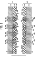
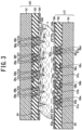
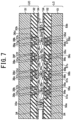
- FIGs. 2 to 7 a method of manufacturing (the method of assembling) the stacked device pertaining to the first embodiment of the present invention will be explained, referring to FIGs. 2 to 7 .
- the method of manufacturing an upper chip UC and a lower chip LC adapted for the stacked device will be described later by using FIGs. 2 to 12 .
- the method of manufacturing the stacked device will be explained as one of the examples, the method of manufacturing the stacked device can be naturally achieved by various manufacturing methods other than the following explanation, including various variation examples, within the scope of the claims.
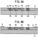
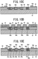
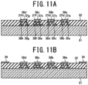
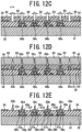
- FIGs. 9A to 12E One example of the method of manufacturing the upper chip UC and the lower chip LC used in the above explanation will be described below referring to FIGs. 9A to 12E .
- the method of manufacturing the stacked device pertaining to the first embodiment of the present invention it is possible to achieve the stacked device in which at the position-aligning accuracy of 0.2 micrometer or less, the upper chip UC is positioned at and stacked on the lower chip LC, and each of the wiring lands 55a, 55b, 55c and 55d in the lower chip LC and each of the tips of the corresponding wiring bumps 35a, 35b, 35c and 35d in the upper chip UC are electrically connected to each other automatically and firmly by the thermal compressive jointing, and the upper chip UC is bonded onto the lower chip LC, in the simple working content.
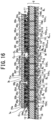
- the interposer 2 includes a silicon substrate 12, a top-insulating film 11 that is formed on a top surface of this silicon substrate 12 and made of silicon oxide film and the like, and a bottom-insulating film 13 that is formed on a bottom surface of the silicon substrate 12 and made of silicon oxide film and the like.
- a plurality of wiring lands 71a to 71o are grouped and arrayed by considering the size of the IC chip.
- Ridged patterns 75a, 75b are arranged at positions outside the array of the wiring lands 71a, 71b, 71c and 71d of a first group.
- Ridged patterns 75c, 75d are arranged at positions outside the array of wiring lands 71e, 71f, 71g and 71h of a second group.
- Ridged patterns 75e, 75f are arranged at positions outside the array of wiring lands 71i, 71j, 71k, ---, 71o of a k-th group.
- Each of the wall-block patterns 75a, 75b; 75c, 75d; 75e, 75f has the inclined planes similar to the wall-block patterns 53a, 53b pertaining to the first embodiment. Similarly to the configuration illustrated in FIG. 8 , even in the stacked device pertaining to the second embodiment, a height of the wall-block patterns 75a, 75b; 75c, 75d; 75e, 75f measured from the reference plane of the interposer 2 is higher than a thickness of the wiring lands 71a to 71o measured from the same reference plane of the interposer 2.
- FIG. 16 exemplifies a configuration in which the wall-block patterns 75a, 75b are arranged at the positions outside the array of the wiring lands 71a, 71b, 71c and 71d of the first group, and the wall-block patterns 75c, 75d are arranged at the positions outside the array of the wiring lands 71e, 71f, 71g and 71h of the second group, and ---, and the wall-block patterns 75e, 75f are arranged at the positions outside the array of the :wiring lands 71i, 71j, 71k, ---, 71o of the k-th group.
- the stacked device pertaining to the second embodiment may be fabricated such that at least one of the wall-block patterns 75a, 75b exists in the inside of the array of the wiring lands 71a, 71b, 71c and 71d of the first group, and at least one of the wall-block patterns 75c, 75d exists in the inside of the array of the wiring lands 71e, 71f, 71g and 71h of the second group, and ---, and at least one of the wall-block patterns 75e, 75f exists in the inside of the array of the wiring lands 71i, 71j, 71k, ---, 71o of the k-th group. That is, the wall-block patterns 75a, 75b; 75c, 75d; 75e, 75f may be arranged at the positions, respectively, except the locations at which the wiring lands 71a to 71o are arrayed.
- the wiring lands 71a to 71o are made of the Au or Au-alloy that contains 80% or more of Au weight percent based on total alloy weight, the behavior of the wiring lands 71a to 71o are preferable with regard to the hardness and the contact resistance.
- a pattern of a hydrophobic film 15a that has the shape of a lens rim adapted for a pair of glasses is delineated selectively in areas.
- an rectangular area in which wiring lands 71a, 71b, 71c and 71d and the wall-block patterns 75a, 75b of the first group are arranged is assigned as one of the rectangular lens-portions
- a rectangular area in which the wiring lands 71e, 71f, 71g and 71h and the wall-block patterns 75c, 75d of the second group are arranged is assigned as the other one of the rectangular lens-portions.
- FIG. 16 shows a pattern in which the pattern of the hydrophobic film 15a and the pattern of the hydrophobic film 15b are independent of each other, for convenience. Actually, a ladder-shaped pattern may be used in which the pattern of the hydrophobic film 15a and the pattern of the hydrophobic film 15b are continuous.
- bottom surface wirings 72a, 72b, ---, 72g are formed, and the bottom surface wiring 72a is electrically connected to an wiring land 71a on the top surface side of the interposer 2 through a through-silicon via TSV 1 that penetrates the top-insulating film 11, the silicon substrate 12 and the bottom-insulating film 13.
- the bottom surface wiring 72b is electrically connected to an wiring land 71d on the top surface side of the interposer 2 through a through-silicon via TSV 2 that penetrates the top-insulating film 11, the silicon substrate 12 and the bottom-insulating film 13, and the bottom surface wiring 72c is electrically connected to an wiring land 71e on the top surface side of the interposer 2 through a through-silicon via TSV 3 that penetrates the top-insulating film 11, the silicon substrate 12 and the bottom-insulating film 13, and the bottom surface wiring 72d is electrically connected to an wiring land 71h on the top surface side of the interposer 2 through a through-silicon via TSV 4 that penetrates the top-insulating film 11, the silicon substrate 12 and the bottom-insulating film 13.
- the bottom surface wiring 72e is electrically connected to an wiring land 71i on the top surface side of the interposer 2 through a through-silicon via TSV (m-2) that penetrates the top-insulating film 11, the silicon substrate 12 and the bottom-insulating film 13, and the bottom surface wiring 72f is electrically connected to the wiring land 71i on the top surface side of the interposer 2 through a through-silicon via TSV (m-1) that penetrates the top-insulating film 11, the silicon substrate 12 and the bottom-insulating film 13, and the bottom surface wiring 72g is electrically connected to an wiring land 71o on the top surface side of the interposer 2 through a through-silicon via TSV m that penetrates the top-insulating film 11, the silicon substrate 12 and the bottom-insulating film 13.
- solder resist 14 is formed so as to bury a part of the bottom surface wirings 72a, 72b, ---, 72g.
- windows are opened to expose the parts of the lower planes of the bottom surface wirings 72a, 72b, ---, 72g, respectively.
- solder bumps B 1 , B 2 , ---, B n are formed to electrically connect with the bottom surface wirings 72a, 72b, ---, 72g, respectively.
- the first IC chip C 1 has wiring bumps 35a, 35b, 35c and 35d assigned correspondingly to the positions of the wiring lands 71a, 71b, 71c and 71d, respectively and the cone bumps 33a, 33b assigned correspondingly to the positions of the wall-block patterns 75a, 75b, respectively.
- each of the tips of the cone bumps 33a, 33b is thinner than the chip side, and a height of the cone bumps 33a, 33b measured from the reference plane of the first IC chip C 1 is higher than a height of the wiring bumps 35a, 35b, 35c and 35d, measured from the reference plane of the first IC chip C 1 .
- a rectangular area, in which the wiring bumps 35a, 35b, 35c and 35d and the cone bumps 33a, 33b are arranged, is surrounded by a rectangular frame-shaped pattern of a hydrophobic film 34a that is formed outside the rectangular area.
- the second IC chip C 2 has wiring bumps 35e, 35f, 35g and 35h assigned correspondingly to the positions of the wiring lands 71e, 71f, 71g and 71h, respectively, and cone bumps 33c, 33d which are assigned correspondingly to the positions of the wall-block patterns 75c, 75d, respectively.
- each of the tips of the cone bumps 33c, 33d is thinner than the chip side of the cone bumps 33c, 33d, and a height of the cone bumps 33c, 33d measured from the reference plane of the chip is higher than a height of the wiring bumps 35e, 35f, 35g and 35h, measured from the reference plane of the second IC chip C 2 .
- a rectangular area in which the wiring bumps 35e, 35f, 35g and 35h and the cone bumps 33c, 33d are arranged is surrounded by a rectangular frame-shaped pattern of a hydrophobic film 34b that is formed outside the rectangular area.
- the k-th IC chip C k has wiring bumps 35i, 35j, 35k, ---, 35o assigned correspondingly to the positions of the wiring lands 71i, 71j, 71k, ---, 71o, respectively, and cone bumps 33e, 33f which are assigned correspondingly to the positions of the wall-block patterns 75e, 75f, respectively.
- each of the tips of the cone bumps 33e, 33f is thinner than the chip side of the cone bumps 33e, 33f, and a height of the cone bumps 33e, 33f measured from the reference plane of the k-th IC chip C k is higher than a height of the wiring bumps 35i, 35j, 35k, ---, 35o, measured from the reference plane of the k-th IC chip C k .
- a rectangular area in which the wiring bumps 35i, 35j, 35k, ---, 35o and the cone bumps 33e, 33f are arranged is surrounded by the rectangular frame-shaped pattern of the hydrophobic film 34a that is formed outside the rectangular area.
- the wiring bumps 35a to 35o and the cone bumps 33a, 33b; 33c, 33d; 33e, 33f are made of the gold or gold-alloy that contains 80% or more of Au weight percent based on total alloy weight, the behavior of the wiring bumps 35a to 35o and the cone bumps 33a, 33b; 33c, 33d; 33e, 33f are preferable with regard to the hardness and the contact resistance.
- the wiring bumps 35a, 35b, 35c and 35d of the first IC chip C 1 are precisely aligned at the positions of the wiring lands 71a, 71b, 71c and 71d of the interposer 2, respectively, and the cone bumps 33a, 33b are precisely aligned at the positions of the wall-block patterns 75a, 75b of the interposer 2, respectively.
- the wiring bumps 35e, 35f, 35g and 35h of the second IC chip C 2 are precisely aligned at the positions of the wiring lands 71e, 71f, 71g and 71h of the interposer 2, respectively, and the cone bumps 33c, 33d are precisely aligned at the positions of the wall-block patterns 75c, 75d of the interposer 2, respectively, and the wiring bumps 35i, 35j, 35k, ---, 35o of the k-th IC chip C k are precisely aligned at the positions of the wiring lands 71i, 71j, 71k, ---, 71o of the interposer 2, respectively, and the cone bumps 33e, 33f are precisely aligned at the positions of the wall-block patterns 75e, 75f of the interposer 2, respectively.
- the wiring bumps 35a, 35b, 35c and 35d of the first IC chip C 1 are thermo-compression bonded to the wiring lands 71a, 71b, 71c and 71d of the interposer 2, respectively, and the wiring bumps 35e, 35f, 35g and 35h of the second IC chip C 2 are thermo-compression bonded to the wiring lands 71e, 71f, 71g and 71h of the interposer 2, respectively, ---, and the wiring bumps 35i, 35j, 35k, ---, 35o of the k-th IC chip C k are thermo-compression bonded to the wiring lands 71i, 71j, 71k, ---, 71o of the interposer 2, respectively.
- the first IC chip C 1 , the second IC chip C 2 , ---, the k-th IC chip C k can be easily bonded to the interposer 2.
- the wall-block patterns 75a, 75b; 75c, 75d; 75e, 75f of the interposer 2 are electrically connected to the electric wiring layers and the like formed on the top-insulating film 11 of the interposer 2, and the cone bumps 33a, 33b are electrically connected to any of the electrical wiring layers of the first IC chip C 1 , and the cone bumps 33c, 33d are electrically connected to any of the electrical wiring layers of the second IC chip C 2 , and the cone bumps 33e, 33f are electrically connected to any of the electrical wiring layers of the k-th IC chip C k .
- any of the cone bumps 33a, 33b; 33c, 33d; 33e, 33f and the corresponding wall-block patterns 75a, 75b; 75c, 75d; 75e, 75f can be used for the electrical connection.
- the whole of the wall-block patterns 75a, 75b; 75c, 75d; 75e, 75f may be made of electrically conductive materials, or the electrical wiring layer may be formed on the surface.
- the interposer 3 may be formed of a flexible resin substrate 16 as a base.
- lower-level inner wirings II 2 , II (j-2) and II (j+1) and upper-level inner wirings II 1 , II 3 , II 4 , II 5 , II (j-1) and II j electrically connected through the resin substrate 16 on the lower-level inner wirings II 2 , II (j-2) and II (j+1) are buried as illustrated in FIG. 17 .
- the resin substrate 16 is represented as if it was a single layer substrate in a rough outlined simple representation illustrated in FIG. 17 , the resin substrate 16 is actually the multilevel structure implemented by triple or quadruple-level insulating layers.
- FIG. 17 exemplifies the inner wiring structure implemented by double layers for simplification, a multilevel inner wiring structure, implemented by triple layers or more, may be employed on the basis of the design-based requirement of the interposer 3.
- Wall-block patterns 76a, 76b are arranged at positions outside the array of the wiring lands 73a, 73b, 73c and 73d of a first group, and wall-block patterns 76c, 76d are arranged at positions outside the array of wiring lands 73e, 73f, 73g and 73h of a second group, and ---, wall-block patterns 76e, 76f are arranged at positions outside the array of wiring lands 73i, 73j, 73k, ---, 73n of a p-th group.
- Each of the wall-block patterns 76a, 76b; 76c, 76d; 76e, 76f has the inclined planes similar to the wall-block patterns 53a, 53b of the stacked device pertaining to the first embodiment.
- at least one of the wall-block patterns 76a, 76b may exist in the inside of the array of the wiring lands 73a, 73b, 73c and 73d of the first group, and at least one of the wall-block patterns 76c, 76d may exist in the inside of the array of the wiring lands 73e, 73f, 73g and 73h of the second group, and ---, at least one of the wall-block patterns 76e, 76f may exist in the inside of the array of the wiring lands 73i, 73j, 73k and 73n of the p-th group. That is, the wall-block patterns 76a, 76b; 76c, 76d; 76
- a height of the wall-block patterns 76a, 76b; 76c, 76d; 76e, 76f measured from the reference plane of the interposer 3 is higher than a thickness of the wiring lands 73a to 73n, measured from the reference plane of the interposer 3.
- Each of the upper-level inner wirings II 1 , II 3 , II 4 , II 5 , II (j-1) and II j and each of the corresponding lower-level inner wirings II 2 , II (j-2) and II (j+1) are connected to each other through via-plugs V 2 , V 3 , V 6 , V (q-2) and V (q+1) , respectively.
- the wiring land 73a formed on the top surface of the interposer 3 and the upper-level inner wiring II 3 are electrically connected to each other through the via-plug V 4 .
- the wiring land 73d and the upper-level inner wiring II 4 are electrically connected to each other through the via-plug V 5
- the wiring land 73e and the upper-level inner wiring II 4 are electrically connected to each other through the via-plug V 7
- the wiring land 73h and the upper-level inner wiring II 5 are electrically connected to each other through the via-plug V 8 .
- the wiring land 73i and the upper-level inner wiring II (j-1) are electrically connected to each other through the via-plug V (q-2)
- the wiring land 73l and the upper-level inner wiring II (j-1) are electrically connected to each other through the via-plug V (q-1)
- the wiring land 73n and the upper-level inner wiring II j are electrically connected to each other through the via-plug V q .
- a pattern of a hydrophobic film 17a that has a shape of a lens rim of a pair of glasses is delineated.
- a rectangular area, where the wiring lands 73a, 73b, 73c and 73d and the wall-block patterns 76a, 76b of the first group are arranged, is assigned as one rectangular lens-portion of the pair of glasses
- a rectangular area, where the wiring lands 73e, 73f, 73g and 73h and the wall-block patterns 76c, 76d of the second group are arranged, is assigned as the other rectangular lens-portion of the pair of glasses.
- the periphery of the rectangular areas is surrounded by the pattern of a hydrophobic film 17a in a double rectangular shape so as to implement the topology of the lens rim of the pair of glasses.
- FIG. 17 shows a pattern in which the pattern of the hydrophobic film 17a and the pattern of the hydrophobic film 17b are independent of each other, for convenience, a ladder-shaped pattern may be used in which the pattern of the hydrophobic film 17a and the pattern of the hydrophobic film 17b are continuous.
- the first IC chip C 1 has wiring bumps 35a, 35b, 35c and 35d assigned correspondingly to the positions of the wiring lands 73a, 73b, 73c and 73d, respectively, and cone bumps 33a, 33b which are assigned correspondingly to the positions of the wall-block patterns 76a, 76b, respectively.
- each of the tips of the cone bumps 33a, 33b is thinner than the chip side of the cone bumps 33a, 33b, and the height of the cone bumps 33a, 33b measured from the reference plane of the first IC chip C 1 is higher than the height of the wiring bumps 35a, 35b, 35c and 35d measured from the reference plane of the first IC chip C 1 .
- a rectangular area in which the wiring bumps 35a, 35b, 35c and 35d and the cone bumps 33a, 33b are arranged is surrounded by the rectangular frame-shaped pattern of the hydrophobic film 34a that is formed outside the rectangular area.
- the second IC chip C 2 has wiring bumps 35e, 35f, 35g and 35h assigned correspondingly to the positions of the wiring lands 73e, 73f, 73g and 73h, respectively, and cone bumps 33c, 33d which are assigned correspondingly to the positions of the wall-block patterns 76c, 76d, respectively.
- each of the tips of the cone bumps 33c, 33d is thinner than the chip side of the cone bumps 33c, 33d, and the height of the cone bumps 33c, 33d measured from the reference plane of the second IC chip C 2 is higher than the height of the wiring bumps 35e, 35f, 35g and 35h, measured from the reference plane of the second IC chip C 2
- a rectangular area in which the wiring bumps 35e, 35f, 35g and 35h and the cone bumps 33c, 33d are arranged is surrounded by the rectangular frame-shaped pattern of the hydrophobic film 34b that is formed outside the rectangular area.
- the p-th IC chip C k has wiring bumps 35i, 35j, 35k, ---, 35n assigned correspondingly to the positions of the wiring lands 73i, 73j, 73k, ---, 73n, respectively, and cone bumps 33e, 33f which are assigned correspondingly to the positions of the wall-block patterns 76e, 76f, respectively.
- each of the tips of the cone bumps 33e, 33f is thinner than the chip side of the cone bumps 33e, 33f, and the height of the cone bumps 33e, 33f measured from the reference plane of the p-th IC chip C p is higher than the height of the wiring bumps 35i, 35j, 35k, ---, 35n, measured from the reference plane of the p-th IC chip C p .
- a rectangular area in which the wiring bumps 35i, 35j, 35k, ---, 35n and the cone bumps 33e, 33f are arranged is surrounded by the rectangular frame-shaped pattern of the hydrophobic film 34a that is formed outside the rectangular area.
- the cone bumps 33a, 33b; 33c, 33d; 33e, 33f and the wiring lands 73a to 73n are made of the gold or gold-alloy that contains 80% or more of Au weight percent based on total alloy weight, the behavior the wiring bumps 35a to 35n, the cone bumps 33a, 33b; 33c, 33d; 33e, 33f and the wiring lands 73a to 73n are preferable with regard to the hardness and the contact resistance.
- the wiring bumps 35a, 35b, 35c and 35d of the first IC chip C 1 are precisely aligned at the positions of the wiring lands 73a, 73b, 73c and 73d of the interposer 3, respectively, and the cone bumps 33a, 33b are precisely aligned at the positions of the wall-block patterns 76a, 76b of the interposer 3, respectively.
- the wiring bumps 35e, 35f, 35g and 35h of the second IC chip C 2 are precisely aligned at the positions of the wiring lands 73e, 73f, 73g and 73h of the interposer 3, respectively, and the cone bumps 33c, 33d are precisely aligned at the positions of the wall-block patterns 76c, 76d of the interposer 3, respectively, and the wiring bumps 35i, 35j, 35k, ---, 35n of the p-th IC chip C k are precisely aligned at the positions of the wiring lands 73i, 73j, 73k, ---, 73n of the interposer 3, respectively, and the cone bumps 33e, 33f are precisely aligned at the positions of the wall-block patterns 76e, 76f of the interposer 3, respectively.
- the wiring bumps 35a, 35b, 35c and 35d of the first IC chip C 1 are thermo-compression bonded to the wiring lands 73a, 73b, 73c and 73d of the interposer 3, respectively, and the wiring bumps 35e, 35f, 35g and 35h of the second IC chip C 2 are thermo-compression bonded to the wiring lands 73e, 73f, 73g and 73h of the interposer 3, respectively, ---, and the wiring bumps 35i, 35j, 35k, ---, 35n of the p-th IC chip C k are thermo-compression bonded to the wiring lands 73i, 73j, 73k, ---, 73n of the interposer 3, respectively.
- the first IC chip C 1 , the second IC chip C 2 , ---, the p-th IC chip C k can be easily bonded to the interposer 3.
- the wall-block patterns 76a, 76b; 76c, 76d; 76e, 76f of the interposer 3 are electrically connected to the upper electric wiring or lower inner wiring and the like of the interposer 3, and the cone bumps 33a, 33b are electrically connected to any of the electrical wiring layers of the first IC chip C 1 , and the cone bumps 33c, 33d are electrically connected to any of the electrical wiring layers of the second IC chip C 2 , and the cone bumps 33e, 33f are electrically connected to any of the electrical wiring layers of the k-th IC chip C k .
- the first to third embodiments describe the engagement between the cone bump and the wall-block pattern, for the case in which as illustrated in FIGs. 13A and 13B , on the center of the wall-block pattern 53p having the shape of the truncated pyramid (the shape of the pyramidal frustum), the pyramidal concave of the apex angle ⁇ 1 defined in the cross-section viewed from the XIII-XIII direction in FIG. 13A is formed, and the value of the apex angle ⁇ 1 is set greater than the apex angle ⁇ 2 ( ⁇ 1 ⁇ ⁇ 2 ) defined in the cross-section viewed from the XIV-XIV direction in FIG.
- FIGs. 18A and 18B a truncated pyramidal wall-block pattern 53q is formed, and on the center of the wall-block pattern 53q, a truncated pyramidal concave of a slant angle ⁇ 1 /2 of a side wall with respect to a perpendicular direction defined in the cross-section viewed from the XVI-XVI direction in FIG.
- the apex of the cone bump 33qi does not arrive at the bottom of the truncated pyramid that implements the concave, which is cut in the center of the wall-block pattern 53q.
- four inclined planes of the cone bump 33qi are engaged with four sides serving as the inner edges of the opening in the top base of t the wall-block pattern 53q, respectively, while they are in contact with each other at the same time.
- the self-alignment is carried out such that the center of the cone bump 33q 1 and the center of the wall-block pattern 53q are aligned. Then, this self-alignment enables the precise alignment of the accuracy of 0.2 micrometer or less.
- the apex angle ⁇ 2 ( ⁇ 1 ⁇ ⁇ 2 ) defined in the cross-section viewed from the XIII-XIII direction in FIG. 20A since the value of the slant angle ⁇ 1 /2 of the side wall of the wall-block pattern 53q illustrated in FIGs. 18A and 18B is set smaller than the apex angle ⁇ 2 ( ⁇ 1 ⁇ ⁇ 2 ) defined in the cross-section viewed from the XIII-XIII direction in FIG. 20A , with regard to a conical cone bump 33q 2 illustrated in FIG. 20B , the apex of the cone bump 33q 2 dose not arrive at the bottom of the truncated pyramid that implements the concave, which is cut in the center of the wall-block pattern 53q.
- the L-shaped wall-block patterns are arranged at four or more locations in a non-hydrophobic area, such as four corners of the area inside the rectangular frame-shaped pattern of the hydrophobic film, and the like, respectively, and an alignment accuracy of the accuracy of 0.2 micrometer or less can be achieved.
- the self-alignment can be carried out such that a part of a inclined plane of a pyramidal or conical cone bump 33s is in contact with a side, defined at the top end of the wall-block pattern 53s.
- the truncated pyramidal wall-block patterns 53r having the linear top base in the plan view, are arranged at the four or more locations, respectively, in the non-hydrophobic area, which is defined in the inside of the rectangular frame-shaped pattern of the hydrophobic film. Consequently, because at least one inclined plane of the pyramidal cone bump 33s or at least one point on circle circumference of the conical cone bump 33s can be brought into contact with the L-shaped wall-block pattern 53r, by providing simultaneous contact at four or more locations, a precise alignment can be achieved by the self-alignment. That is, even in the case of the truncated pyramidal wall-block pattern 53s as illustrated in FIG. 22 , an alignment accuracy of the accuracy of 0.2 micrometer or less can be achieved.
- the L-shaped wall-block pattern 53r illustrated in FIGs. 21A and 21B is conceptually extended and generalized, it is allowable to use truncated pyramidal wall-block patterns 53ti, 53t 2 that exhibit a couple of linear patterns, each of the longitudinal directions of the linear patterns is orthogonal to each other in a plan view, as illustrated in FIG. 23 .
- the two wall-block patterns 53t 1 , 53t 2 are allocated as a plurality of pairs.
- Each of the linear patterns 53t 1 , 53t 2 in each of the pairs is disposed at a distance shorter than the dimension of the thick portion on the chip side of a cone bump 33t, so that the linear patterns 53t 1 , 53t 2 are arranged close to each other in each of the pairs.
- two inclined planes of each of the pyramidal cone bumps 33t or two points on the circular circumference of each of the conical cone bumps 33t are brought into contact simultaneously, the two contact points are defined at four or more locations, respectively, so that a precise alignment can be carried out by the self-alignment. That is, even in the case of the topology implemented by a pair of truncated pyramidal wall-block patterns 53t 1 , 53t 2 illustrated in FIG.
- each of the wall-block patterns 53t 1 , 53t 2 is arranged close to each other in each of the pairs, by disposing a plurality of pairs at four or more locations, respectively, an alignment accuracy of the accuracy of 0.2 micrometer or less can be achieved.
- the two truncated conical wall-block patterns 53u 1 , 53u 2 that are arranged close to each other at a distance shorter than the dimension of the thick portion on the chip side of the cone bump 33u are allocated as a pair, and a plurality of pairs are arranged at the four or more locations, respectively, in the non-hydrophobic area, which is defined in the inside of the pattern of the hydrophobic film.
- the precise alignment can be achieved by the self-alignment, because two inclined planes or two points on the circular circumference of the cone bump 33 are brought into contact simultaneously, the two contact points are defined at four or more locations, respectively.
Landscapes
- Internal Circuitry In Semiconductor Integrated Circuit Devices (AREA)
- Engineering & Computer Science (AREA)
- Manufacturing & Machinery (AREA)
- Wire Bonding (AREA)
Claims (13)
- Gestapelte Vorrichtung, umfassend:einen unteren Chip (LC), der eine Vielzahl von Verdrahtungsfeldern (55a, 55b, 55c, 55d) und eine Vielzahl von Wand-Block-Mustern (53a, 53b) einschließt, wobei jedes der Wand-Block-Muster einer Position mit Ausnahme von Stellen zugewiesen ist, an denen die Verdrahtungsfelder angeordnet sind, wobei jedes der Wand-Block-Muster eine geneigte Ebene aufweist, wobei eine Höhe jedes der Wand-Block-Muster, gemessen von einer Referenzebene eines Arrays der Vielzahl von Verdrahtungsfeldern, höher ist als die Verdrahtungsfelder; undeinen oberen Chip (UC), der eine Vielzahl von Verdrahtungserhebungen (35a, 35b, 35c, 35d), die jeweils entsprechend den Positionen der Verdrahtungsfelder zugeordnet sind, und eine Vielzahl von pyramidenförmigen oder konischen Kegelerhebungen (33a, 33b), die jeweils entsprechend den Positionen der Wand-Block-Muster zugeordnet sind, einschließt;wobei die gestapelte Vorrichtung dadurch gekennzeichnet ist, dassein erster hydrophober Film (54) in einer Peripherie des unteren Chips abgegrenzt ist, der konfiguriert ist, um das Array der Verdrahtungsfelder und der Wand-Block-Muster zu umgeben, und ein zweiter hydrophober Film (34) in einer Peripherie des oberen Chips abgegrenzt ist, der konfiguriert ist, um ein Array der Vielzahl der Verdrahtungserhebungen und der Vielzahl der Kegelerhebungen zu umgeben; und dadurch, dassein Wand-Block-Muster (53p) eine pyramidenförmige Konkavität mit einem Querschnittsscheitelwinkel α1 aufweist, der größer ist als ein Querschnittsscheitelwinkel α2 einer Kegelerhebung (33p1, 33p2), die der Position dieses Wand-Block-Musters (53p) zugeordnet ist;oderein Wand-Block-Muster (53q) eine trunkierte pyramidenförmige Konkavität mit einem Querschnittsneigungswinkel der Seitenwand β1/2 aufweist und eine Kegelerhebung (33q1, 33q2), die der Position dieses Wand-Block-Musters (53q) zugeordnet ist, einen Querschnittsscheitelwinkel β2 aufweist und β1 ≤ β2.
- Gestapelte Vorrichtung nach Anspruch 1, wobei die Vielzahl von Wand-Block-Mustern jeweils an Positionen außerhalb des Arrays der Verdrahtungsfelder eingerichtet ist.
- Gestapelte Vorrichtung nach Anspruch 1, wobei mindestens eines der Wand-Block-Muster jeweils an Positionen innerhalb des Arrays der Verdrahtungsfelder eingerichtet ist.
- Gestapelte Vorrichtung nach Anspruch 1, wobei die Vielzahl von Wand-Block-Mustern und die Vielzahl von Kegelerhebungen jeweils in Kontakt miteinander sind und der Kontakt als eine elektrische Verbindung verwendet wird.
- Gestapelte Vorrichtung nach Anspruch 1, wobei jede der geneigten Ebenen der Wand-Block-Muster jeweils eine der Seitenwände von Konkavitäten implementiert, die in einem Zentrum in jedem der Wand-Block-Muster ausgebildet sind.
- Gestapelte Vorrichtung nach Anspruch 1, wobei die Verdrahtungsfelder, die Verdrahtungserhebungen und die Kegelerhebungen aus Gold oder einer Goldlegierung hergestellt sind, die 80 Gewichtsprozent Gold basierend auf dem Gesamtgewicht der Legierung oder mehr enthält.
- Gestapelte Vorrichtung, umfassendeinen Interposer (2), der eine Vielzahl von Verdrahtungsfeldern (71a bis 71o) und eine Vielzahl von Wand-Block-Mustern einschließt, wobei jedes der Wand-Block-Muster (75a, 75b) einer Position mit Ausnahme von Stellen zugewiesen ist, an denen die Verdrahtungsfelder angeordnet sind, wobei jedes der Wand-Block-Muster eine geneigte Ebene aufweist, wobei eine Höhe jedes der Wand-Block-Muster, gemessen von einer Referenzebene eines Arrays der Vielzahl von Verdrahtungsfeldern, höher ist als die Verdrahtungsfelder; undeinen IC-Chip (C1), der eine Vielzahl von Verdrahtungserhebungen (35a, 35b, 35c, 35d), die jeweils entsprechend den Positionen der Verdrahtungsfelder zugeordnet sind, und eine Vielzahl von pyramidenförmigen oder konischen Kegelerhebungen (33a, 33b), die jeweils entsprechend den Positionen der Wand-Block-Muster zugeordnet sind, einschließt;wobei die gestapelte Vorrichtung dadurch gekennzeichnet ist, dassein erster hydrophober Film (15a) in einer Peripherie des Interposers abgegrenzt ist, der konfiguriert ist, um das Array der Verdrahtungsfelder und der Wand-Block-Muster zu umgeben, denen die Verdrahtungserhebungen und die Kegelerhebungen des IC-Chips zugeordnet sind,und ein zweiter hydrophober Film (15b) in einer Peripherie des oberen Chips abgegrenzt ist, der konfiguriert ist, um ein Array von der Vielzahl der Verdrahtungserhebungen und der Vielzahl von Kegelerhebungen zu umgeben; und dadurch, dassein Wand-Block-Muster (53p) eine pyramidenförmige Konkavität mit einem Querschnittsscheitelwinkel α1 aufweist, der größer ist als ein Querschnittsscheitelwinkel α2 einer Kegelerhebung (33p1, 33p2), die der Position dieses Wand-Block-Musters (53p) zugeordnet ist;oderein Wand-Block-Muster (53q) eine trunkierte pyramidenförmige Konkavität mit einem Querschnittsneigungswinkel β1/2 der Seitenwand aufweist und eine Kegelerhebung (33q1, 33q2), die der Position dieses Wand-Block-Musters (53q) zugeordnet ist, einen Querschnittsscheitelwinkel β2 aufweist und β1 ≤ β2.
- Gestapelte Vorrichtung nach Anspruch 7, wobei die Vielzahl von Wand-Block-Mustern jeweils an Positionen außerhalb des Arrays der Verdrahtungsfelder eingerichtet ist.
- Gestapelte Vorrichtung nach Anspruch 7, wobei die Vielzahl von Wand-Block-Mustern und die Vielzahl von Kegelerhebungen jeweils in Kontakt miteinander sind und der Kontakt als eine elektrische Verbindung verwendet wird.
- Gestapelte Vorrichtung nach Anspruch 7, wobei jede der geneigten Ebenen der Wand-Block-Muster jeweils eine der Seitenwände von Konkavitäten implementiert, die in einem Zentrum in jedem der Wand-Block-Muster ausgebildet sind.
- Gestapelte Vorrichtung nach Anspruch 7, wobei die Verdrahtungsfelder, die Verdrahtungserhebungen und die Kegelerhebungen aus Gold oder einer Goldlegierung hergestellt sind, die 80 Gewichtsprozent Gold basierend auf dem Gesamtgewicht der Legierung oder mehr enthält.
- Gestapelte Vorrichtung nach Anspruch 7, wobei ein von den Verdrahtungsfeldern und den Wand-Block-Mustern ausgebildetes Array eines aus einer Vielzahl von Arrays von Verdrahtungsfeldern und Wand-Block-Mustern ist, die in dem Interposer eingeschlossen und in Gruppen gruppiert sind, wobei der IC-Chip einer aus einer Vielzahl von oberen Chips ist, die auf dem Interposer montiert sind, wobei jeder weitere obere Chip ein Array von Verdrahtungserhebungen und Kegelerhebungen einschließt, die einer der Gruppen von Verdrahtungsfeldern und Wand-Block-Mustern zugeordnet sind; und wobei ein weiterer erster hydrophober Film selektiv in einem Teil einer Oberfläche des Interposers abgegrenzt ist, der konfiguriert ist, um jede der Gruppen von Verdrahtungsfeldern und Wand-Block-Mustern zu umgeben,
wobei ein weiterer zweiter hydrophober Film jeweils in jedem oberen Chip ausgebildet ist und konfiguriert ist, um jedes der Arrays von Verdrahtungserhebungen und Kegelerhebungen jeweils zu umgeben. - Verfahren zur Herstellung einer gestapelten Vorrichtung, das Folgendes einschließt:selektives Auftragen einer Flüssigkeit auf einen unteren Chip (LC), der eine Vielzahl von Verdrahtungsfeldern (55a, 55b, 55c, 55d) und eine Vielzahl von Wand-Block-Mustern (53a, 53b) aufweist, die jeweils an Positionen mit Ausnahme von Stellen, an denen die Verdrahtungsfelder angeordnet sind, eingerichtet sind, und wobei jedes der Wand-Block-Muster jeweils eine geneigte Ebene aufweist und einen ersten hydrophoben Film (54) aufweist, der in einer Peripherie des unteren Chips abgegrenzt ist, der konfiguriert ist, um ein Array der Verdrahtungsfelder und der Wand-Block-Muster zu umgeben;Zusammenfügen eines oberen Chips (UC), der eine Vielzahl von Verdrahtungserhebungen (35a, 35b, 35c, 35d) aufweist, die jeweils entsprechend den Positionen der Verdrahtungsfelder zugeordnet sind, mit einer Vielzahl von pyramidenförmigen oder konischen Kegelerhebungen (33a, 33b), die jeweils entsprechend den Positionen der Vielzahl von Wand-Block-Mustern zugeordnet sind, und einen zweiten hydrophoben Film (34) aufweisen, der in einer Peripherie des oberen Chips abgegrenzt ist, der konfiguriert ist, um ein Array der Vielzahl von Verdrahtungserhebungen und der Vielzahl von Kegelerhebungen zu umgeben,wobei ein Wand-Block-Muster (53p) eine pyramidenförmige Konkavität mit einem Querschnittsscheitelwinkel α1 aufweist, der größer ist als ein Querschnittsscheitelwinkel α2 einer Kegelerhebung (33p1, 33p2), die der Position dieses Wand-Block-Musters (53p) zugeordnet ist, oder ein Wand-Block-Muster (53q) eine trunkierte pyramidenförmige Konkavität mit einem Querschnittsneigungswinkel der Seitenwand β1/2 aufweist und eine Kegelerhebung (33q1, 33q2), die der Position dieses Wand-Block-Musters (53q) zugeordnet ist, einen Querschnittsscheitelwinkel β2 aufweist und β1 ≤ β2;sodass jede der Verdrahtungserhebungen der Vielzahl von Verdrahtungsfeldern jeweils durch einen Tropfen der aufgetragenen Flüssigkeit zugewandt ist;jeweils Selbstausrichten der Position der Vielzahl von Verdrahtungserhebungen zu den Positionen der Verdrahtungsfelder und jeweils Selbstausrichten der Position der Vielzahl von Kegelerhebungen zu den Positionen der Wand-Block-Muster durch die Oberflächenspannung der Flüssigkeit;Ausüben eines Drucks, sodass der obere Chip gegen den unteren Chip gedrückt wird und die Spitzen der Vielzahl von Verdrahtungserhebungen jeweils in Kontakt mit den Verdrahtungsfeldern in dem selbstausgerichteten Zustand gebracht werden und die Vielzahl von Kegelerhebungen jeweils in Kontakt mit den geneigten Ebenen der Vielzahl von Wand-Block-Mustern gebracht werden; undVerdampfen der Flüssigkeit.
Applications Claiming Priority (1)
| Application Number | Priority Date | Filing Date | Title |
|---|---|---|---|
| PCT/JP2013/056330 WO2014136241A1 (ja) | 2013-03-07 | 2013-03-07 | 積層体及びその製造方法 |
Publications (3)
| Publication Number | Publication Date |
|---|---|
| EP2966680A1 EP2966680A1 (de) | 2016-01-13 |
| EP2966680A4 EP2966680A4 (de) | 2016-11-30 |
| EP2966680B1 true EP2966680B1 (de) | 2024-08-28 |
Family
ID=51486854
Family Applications (1)
| Application Number | Title | Priority Date | Filing Date |
|---|---|---|---|
| EP13877188.6A Active EP2966680B1 (de) | 2013-03-07 | 2013-03-07 | Gestapelte anordnung und verfahren zur herstellung davon |
Country Status (4)
| Country | Link |
|---|---|
| US (1) | US9219047B2 (de) |
| EP (1) | EP2966680B1 (de) |
| JP (1) | JP6306568B2 (de) |
| WO (1) | WO2014136241A1 (de) |
Families Citing this family (29)
| Publication number | Priority date | Publication date | Assignee | Title |
|---|---|---|---|---|
| US9557370B2 (en) * | 2012-02-10 | 2017-01-31 | Taiwan Semiconductor Manufacturing Company, Ltd. | Methods of improving bump allocation for semiconductor devices and semiconductor devices with improved bump allocation |
| US9773724B2 (en) * | 2013-01-29 | 2017-09-26 | Taiwan Semiconductor Manufacturing Company, Ltd. | Semiconductor devices, methods of manufacture thereof, and semiconductor device packages |
| US10011478B2 (en) * | 2015-05-18 | 2018-07-03 | Innovative Micro Technology | Thermocompression bonding with raised feature |
| US10468363B2 (en) * | 2015-08-10 | 2019-11-05 | X-Celeprint Limited | Chiplets with connection posts |
| US10103069B2 (en) | 2016-04-01 | 2018-10-16 | X-Celeprint Limited | Pressure-activated electrical interconnection by micro-transfer printing |
| US10222698B2 (en) * | 2016-07-28 | 2019-03-05 | X-Celeprint Limited | Chiplets with wicking posts |
| US11064609B2 (en) | 2016-08-04 | 2021-07-13 | X Display Company Technology Limited | Printable 3D electronic structure |
| US10748864B2 (en) * | 2016-10-05 | 2020-08-18 | Semiconductor Components Industries, Llc | Bonded semiconductor package and related methods |
| US10490493B2 (en) | 2016-12-30 | 2019-11-26 | Innolux Corporation | Package structure and manufacturing method thereof |
| CN108538812A (zh) * | 2017-03-06 | 2018-09-14 | 群创光电股份有限公司 | 封装结构 |
| US20180254257A1 (en) * | 2017-03-06 | 2018-09-06 | Innolux Corporation | Package structure and method of manufacturing package structure |
| JP6858939B2 (ja) | 2017-04-28 | 2021-04-14 | 東北マイクロテック株式会社 | 外部接続機構、半導体装置及び積層パッケージ |
| KR20200112851A (ko) * | 2017-12-22 | 2020-10-05 | 보드 오브 리전츠, 더 유니버시티 오브 텍사스 시스템 | 나노스케일 정렬된 삼차원 적층 집적 회로 |
| CN111615745A (zh) * | 2018-02-23 | 2020-09-01 | 富士胶片株式会社 | 接合体的制造方法、临时固定部件及层叠体 |
| JP7174443B2 (ja) * | 2018-06-13 | 2022-11-17 | 国立研究開発法人産業技術総合研究所 | 電子回路の接続方法及び電子回路 |
| US10796971B2 (en) | 2018-08-13 | 2020-10-06 | X Display Company Technology Limited | Pressure-activated electrical interconnection with additive repair |
| US10573544B1 (en) | 2018-10-17 | 2020-02-25 | X-Celeprint Limited | Micro-transfer printing with selective component removal |
| US10796938B2 (en) * | 2018-10-17 | 2020-10-06 | X Display Company Technology Limited | Micro-transfer printing with selective component removal |
| JP7232502B2 (ja) * | 2018-10-29 | 2023-03-03 | 国立研究開発法人産業技術総合研究所 | 微細金属バンプの形成方法及び微細金属バンプ |
| EP3796367A4 (de) * | 2018-11-21 | 2022-03-23 | Tohoku-Microtec Co., Ltd | Gestapelte halbleitervorrichtung und mehrere darin verwendete chips |
| EP3671812B1 (de) * | 2018-12-19 | 2022-02-09 | IMEC vzw | Verfahren zum bonden und verbinden von halbleiterchips |
| CN111584378B (zh) * | 2019-02-19 | 2022-07-12 | 昆山微电子技术研究院 | 一种插入式热压键合方法 |
| JP2020149992A (ja) * | 2019-03-11 | 2020-09-17 | 浜松ホトニクス株式会社 | 半導体装置及び半導体装置の製造方法 |
| US11495562B2 (en) * | 2019-12-27 | 2022-11-08 | Attollo Engineering, LLC | Alignment features for hybridized image sensor |
| US11495561B2 (en) | 2020-05-11 | 2022-11-08 | X Display Company Technology Limited | Multilayer electrical conductors for transfer printing |
| CN113658880B (zh) * | 2020-05-12 | 2025-06-17 | 联华电子股份有限公司 | 芯片键合应力的测量方法及芯片键合辅助结构 |
| CN113594119B (zh) * | 2021-06-25 | 2024-05-14 | 苏州汉天下电子有限公司 | 半导体封装及其制造方法 |
| JP7717631B2 (ja) * | 2022-01-25 | 2025-08-04 | 株式会社東芝 | 電子装置及びその製造方法 |
| DE102022102367A1 (de) * | 2022-02-01 | 2023-08-03 | OSRAM Opto Semiconductors Gesellschaft mit beschränkter Haftung | Zielträger, halbleiteranordnung und verfahren zum transferieren eines halbleiterbauelements und haltestruktur |
Family Cites Families (20)
| Publication number | Priority date | Publication date | Assignee | Title |
|---|---|---|---|---|
| JPS6197932A (ja) * | 1984-10-19 | 1986-05-16 | Hitachi Ltd | 圧着型半導体パツケ−ジ |
| JP2000252413A (ja) * | 1999-02-26 | 2000-09-14 | Rohm Co Ltd | 半導体装置 |
| US6917219B2 (en) * | 2003-03-12 | 2005-07-12 | Xilinx, Inc. | Multi-chip programmable logic device having configurable logic circuitry and configuration data storage on different dice |
| JP2005340738A (ja) * | 2004-05-31 | 2005-12-08 | Matsushita Electric Ind Co Ltd | 半導体装置及びその製造方法 |
| WO2006077739A1 (ja) * | 2004-12-28 | 2006-07-27 | Mitsumasa Koyanagi | 自己組織化機能を用いた集積回路装置の製造方法及び製造装置 |
| US7332423B2 (en) * | 2005-06-29 | 2008-02-19 | Intel Corporation | Soldering a die to a substrate |
| JP5187714B2 (ja) * | 2006-07-11 | 2013-04-24 | 独立行政法人産業技術総合研究所 | 半導体チップの電極接続構造 |
| US7871865B2 (en) * | 2007-01-24 | 2011-01-18 | Analog Devices, Inc. | Stress free package and laminate-based isolator package |
| JP2010040884A (ja) * | 2008-08-07 | 2010-02-18 | Shinkawa Ltd | 半導体装置及び半導体チップのボンディング方法 |
| KR101481577B1 (ko) * | 2008-09-29 | 2015-01-13 | 삼성전자주식회사 | 잉크 젯 방식의 댐을 구비하는 반도체 패키지 및 그 제조방법 |
| JP5417850B2 (ja) * | 2009-01-05 | 2014-02-19 | 住友電気工業株式会社 | 検出装置およびその製造方法 |
| JP5389490B2 (ja) | 2009-03-23 | 2014-01-15 | 東京エレクトロン株式会社 | 三次元集積回路の製造方法及び装置 |
| US20100248424A1 (en) * | 2009-03-27 | 2010-09-30 | Intellectual Business Machines Corporation | Self-Aligned Chip Stacking |
| US8460794B2 (en) * | 2009-07-10 | 2013-06-11 | Seagate Technology Llc | Self-aligned wafer bonding |
| JP5307669B2 (ja) * | 2009-09-09 | 2013-10-02 | 東京エレクトロン株式会社 | 半導体装置の製造方法及び電気的接続を得る方法 |
| KR101624973B1 (ko) * | 2009-09-23 | 2016-05-30 | 삼성전자주식회사 | 패키지 온 패키지 타입의 반도체 패키지 및 그 제조방법 |
| US8115319B2 (en) * | 2010-03-04 | 2012-02-14 | Powertech Technology Inc. | Flip chip package maintaining alignment during soldering |
| JP2011192663A (ja) * | 2010-03-11 | 2011-09-29 | Tokyo Electron Ltd | 実装方法及び実装装置 |
| US20120020040A1 (en) * | 2010-07-26 | 2012-01-26 | Lin Paul T | Package-to-package stacking by using interposer with traces, and or standoffs and solder balls |
| US8338945B2 (en) * | 2010-10-26 | 2012-12-25 | Taiwan Semiconductor Manufacturing Company, Ltd. | Molded chip interposer structure and methods |
-
2013
- 2013-03-07 JP JP2015504070A patent/JP6306568B2/ja active Active
- 2013-03-07 WO PCT/JP2013/056330 patent/WO2014136241A1/ja not_active Ceased
- 2013-03-07 EP EP13877188.6A patent/EP2966680B1/de active Active
-
2014
- 2014-01-30 US US14/168,897 patent/US9219047B2/en active Active
Also Published As
| Publication number | Publication date |
|---|---|
| US20140252604A1 (en) | 2014-09-11 |
| EP2966680A1 (de) | 2016-01-13 |
| WO2014136241A1 (ja) | 2014-09-12 |
| JP6306568B2 (ja) | 2018-04-04 |
| JPWO2014136241A1 (ja) | 2017-02-09 |
| EP2966680A4 (de) | 2016-11-30 |
| US9219047B2 (en) | 2015-12-22 |
Similar Documents
| Publication | Publication Date | Title |
|---|---|---|
| EP2966680B1 (de) | Gestapelte anordnung und verfahren zur herstellung davon | |
| US10453819B2 (en) | Method for fabricating glass substrate package | |
| KR101562705B1 (ko) | 금속 범프 및 그 제조 방법 | |
| CN102456650B (zh) | 半导体基板的导电结构以及其制造方法 | |
| CN102332434B (zh) | 半导体结构及形成元件的方法 | |
| JP7570410B2 (ja) | はんだ接合部間の架橋の防止 | |
| JP7617906B2 (ja) | 基板への側面接続を含む相互接続 | |
| US12021051B2 (en) | Semiconductor package and method of forming the same | |
| JP5568357B2 (ja) | 半導体装置及びその製造方法 | |
| TWI414047B (zh) | 電子元件封裝結構及其製造方法 | |
| US9622347B2 (en) | Wiring substrate, semiconductor device, method of manufacturing wiring substrate, and method of manufacturing semiconductor device | |
| US20140144690A1 (en) | Method for producing a structure for microelectronic device assembly | |
| US20030173678A1 (en) | Semiconductor device and method for fabricating the same | |
| KR20230006531A (ko) | 무범프 초전도체 디바이스 | |
| US9263376B2 (en) | Chip interposer, semiconductor device, and method for manufacturing a semiconductor device | |
| US11574817B2 (en) | Fabricating an interconnection using a sacrificial layer | |
| CN203277371U (zh) | 半导体器件和半导体组件 | |
| CN113725192A (zh) | 半导体封装装置 | |
| JP2012129376A (ja) | 半導体装置 |
Legal Events
| Date | Code | Title | Description |
|---|---|---|---|
| PUAI | Public reference made under article 153(3) epc to a published international application that has entered the european phase |
Free format text: ORIGINAL CODE: 0009012 |
|
| 17P | Request for examination filed |
Effective date: 20151005 |
|
| AK | Designated contracting states |
Kind code of ref document: A1 Designated state(s): AL AT BE BG CH CY CZ DE DK EE ES FI FR GB GR HR HU IE IS IT LI LT LU LV MC MK MT NL NO PL PT RO RS SE SI SK SM TR |
|
| AX | Request for extension of the european patent |
Extension state: BA ME |
|
| DAX | Request for extension of the european patent (deleted) | ||
| A4 | Supplementary search report drawn up and despatched |
Effective date: 20161103 |
|
| RIC1 | Information provided on ipc code assigned before grant |
Ipc: H01L 25/18 20060101ALI20161027BHEP Ipc: H01L 25/07 20060101ALI20161027BHEP Ipc: H01L 25/065 20060101AFI20161027BHEP Ipc: H01L 21/60 20060101ALI20161027BHEP |
|
| STAA | Information on the status of an ep patent application or granted ep patent |
Free format text: STATUS: EXAMINATION IS IN PROGRESS |
|
| 17Q | First examination report despatched |
Effective date: 20191203 |
|
| GRAP | Despatch of communication of intention to grant a patent |
Free format text: ORIGINAL CODE: EPIDOSNIGR1 |
|
| STAA | Information on the status of an ep patent application or granted ep patent |
Free format text: STATUS: GRANT OF PATENT IS INTENDED |
|
| RIC1 | Information provided on ipc code assigned before grant |
Ipc: H01L 21/98 20060101ALI20231218BHEP Ipc: H01L 21/60 20060101ALI20231218BHEP Ipc: H01L 23/544 20060101ALI20231218BHEP Ipc: H01L 23/14 20060101ALI20231218BHEP Ipc: H01L 23/498 20060101ALI20231218BHEP Ipc: H01L 25/065 20060101AFI20231218BHEP |
|
| INTG | Intention to grant announced |
Effective date: 20240115 |
|
| GRAJ | Information related to disapproval of communication of intention to grant by the applicant or resumption of examination proceedings by the epo deleted |
Free format text: ORIGINAL CODE: EPIDOSDIGR1 |
|
| STAA | Information on the status of an ep patent application or granted ep patent |
Free format text: STATUS: EXAMINATION IS IN PROGRESS |
|
| GRAP | Despatch of communication of intention to grant a patent |
Free format text: ORIGINAL CODE: EPIDOSNIGR1 |
|
| STAA | Information on the status of an ep patent application or granted ep patent |
Free format text: STATUS: GRANT OF PATENT IS INTENDED |
|
| INTC | Intention to grant announced (deleted) | ||
| INTG | Intention to grant announced |
Effective date: 20240411 |
|
| GRAS | Grant fee paid |
Free format text: ORIGINAL CODE: EPIDOSNIGR3 |
|
| GRAA | (expected) grant |
Free format text: ORIGINAL CODE: 0009210 |
|
| STAA | Information on the status of an ep patent application or granted ep patent |
Free format text: STATUS: THE PATENT HAS BEEN GRANTED |
|
| AK | Designated contracting states |
Kind code of ref document: B1 Designated state(s): AL AT BE BG CH CY CZ DE DK EE ES FI FR GB GR HR HU IE IS IT LI LT LU LV MC MK MT NL NO PL PT RO RS SE SI SK SM TR |
|
| REG | Reference to a national code |
Ref country code: GB Ref legal event code: FG4D |
|
| REG | Reference to a national code |
Ref country code: CH Ref legal event code: EP |
|
| REG | Reference to a national code |
Ref country code: DE Ref legal event code: R096 Ref document number: 602013086034 Country of ref document: DE |
|
| REG | Reference to a national code |
Ref country code: IE Ref legal event code: FG4D |
|
| REG | Reference to a national code |
Ref country code: DE Ref legal event code: R079 Ref document number: 602013086034 Country of ref document: DE Free format text: PREVIOUS MAIN CLASS: H01L0025065000 Ipc: H10D0080300000 |
|
| REG | Reference to a national code |
Ref country code: LT Ref legal event code: MG9D |
|
| PG25 | Lapsed in a contracting state [announced via postgrant information from national office to epo] |
Ref country code: NO Free format text: LAPSE BECAUSE OF FAILURE TO SUBMIT A TRANSLATION OF THE DESCRIPTION OR TO PAY THE FEE WITHIN THE PRESCRIBED TIME-LIMIT Effective date: 20241128 |
|
| REG | Reference to a national code |
Ref country code: AT Ref legal event code: MK05 Ref document number: 1718969 Country of ref document: AT Kind code of ref document: T Effective date: 20240828 |
|
| PG25 | Lapsed in a contracting state [announced via postgrant information from national office to epo] |
Ref country code: NL Free format text: LAPSE BECAUSE OF FAILURE TO SUBMIT A TRANSLATION OF THE DESCRIPTION OR TO PAY THE FEE WITHIN THE PRESCRIBED TIME-LIMIT Effective date: 20240828 Ref country code: GR Free format text: LAPSE BECAUSE OF FAILURE TO SUBMIT A TRANSLATION OF THE DESCRIPTION OR TO PAY THE FEE WITHIN THE PRESCRIBED TIME-LIMIT Effective date: 20241129 Ref country code: PT Free format text: LAPSE BECAUSE OF FAILURE TO SUBMIT A TRANSLATION OF THE DESCRIPTION OR TO PAY THE FEE WITHIN THE PRESCRIBED TIME-LIMIT Effective date: 20241230 Ref country code: FI Free format text: LAPSE BECAUSE OF FAILURE TO SUBMIT A TRANSLATION OF THE DESCRIPTION OR TO PAY THE FEE WITHIN THE PRESCRIBED TIME-LIMIT Effective date: 20240828 Ref country code: PL Free format text: LAPSE BECAUSE OF FAILURE TO SUBMIT A TRANSLATION OF THE DESCRIPTION OR TO PAY THE FEE WITHIN THE PRESCRIBED TIME-LIMIT Effective date: 20240828 |
|
| PG25 | Lapsed in a contracting state [announced via postgrant information from national office to epo] |
Ref country code: BG Free format text: LAPSE BECAUSE OF FAILURE TO SUBMIT A TRANSLATION OF THE DESCRIPTION OR TO PAY THE FEE WITHIN THE PRESCRIBED TIME-LIMIT Effective date: 20240828 |
|
| PG25 | Lapsed in a contracting state [announced via postgrant information from national office to epo] |
Ref country code: LV Free format text: LAPSE BECAUSE OF FAILURE TO SUBMIT A TRANSLATION OF THE DESCRIPTION OR TO PAY THE FEE WITHIN THE PRESCRIBED TIME-LIMIT Effective date: 20240828 |
|
| REG | Reference to a national code |
Ref country code: NL Ref legal event code: MP Effective date: 20240828 |
|
| PG25 | Lapsed in a contracting state [announced via postgrant information from national office to epo] |
Ref country code: AT Free format text: LAPSE BECAUSE OF FAILURE TO SUBMIT A TRANSLATION OF THE DESCRIPTION OR TO PAY THE FEE WITHIN THE PRESCRIBED TIME-LIMIT Effective date: 20240828 Ref country code: IS Free format text: LAPSE BECAUSE OF FAILURE TO SUBMIT A TRANSLATION OF THE DESCRIPTION OR TO PAY THE FEE WITHIN THE PRESCRIBED TIME-LIMIT Effective date: 20241228 |
|
| PG25 | Lapsed in a contracting state [announced via postgrant information from national office to epo] |
Ref country code: HR Free format text: LAPSE BECAUSE OF FAILURE TO SUBMIT A TRANSLATION OF THE DESCRIPTION OR TO PAY THE FEE WITHIN THE PRESCRIBED TIME-LIMIT Effective date: 20240828 |
|
| PG25 | Lapsed in a contracting state [announced via postgrant information from national office to epo] |
Ref country code: ES Free format text: LAPSE BECAUSE OF FAILURE TO SUBMIT A TRANSLATION OF THE DESCRIPTION OR TO PAY THE FEE WITHIN THE PRESCRIBED TIME-LIMIT Effective date: 20240828 Ref country code: RS Free format text: LAPSE BECAUSE OF FAILURE TO SUBMIT A TRANSLATION OF THE DESCRIPTION OR TO PAY THE FEE WITHIN THE PRESCRIBED TIME-LIMIT Effective date: 20241128 |
|
| PG25 | Lapsed in a contracting state [announced via postgrant information from national office to epo] |
Ref country code: RS Free format text: LAPSE BECAUSE OF FAILURE TO SUBMIT A TRANSLATION OF THE DESCRIPTION OR TO PAY THE FEE WITHIN THE PRESCRIBED TIME-LIMIT Effective date: 20241128 Ref country code: PT Free format text: LAPSE BECAUSE OF FAILURE TO SUBMIT A TRANSLATION OF THE DESCRIPTION OR TO PAY THE FEE WITHIN THE PRESCRIBED TIME-LIMIT Effective date: 20241230 Ref country code: PL Free format text: LAPSE BECAUSE OF FAILURE TO SUBMIT A TRANSLATION OF THE DESCRIPTION OR TO PAY THE FEE WITHIN THE PRESCRIBED TIME-LIMIT Effective date: 20240828 Ref country code: NO Free format text: LAPSE BECAUSE OF FAILURE TO SUBMIT A TRANSLATION OF THE DESCRIPTION OR TO PAY THE FEE WITHIN THE PRESCRIBED TIME-LIMIT Effective date: 20241128 Ref country code: NL Free format text: LAPSE BECAUSE OF FAILURE TO SUBMIT A TRANSLATION OF THE DESCRIPTION OR TO PAY THE FEE WITHIN THE PRESCRIBED TIME-LIMIT Effective date: 20240828 Ref country code: LV Free format text: LAPSE BECAUSE OF FAILURE TO SUBMIT A TRANSLATION OF THE DESCRIPTION OR TO PAY THE FEE WITHIN THE PRESCRIBED TIME-LIMIT Effective date: 20240828 Ref country code: IS Free format text: LAPSE BECAUSE OF FAILURE TO SUBMIT A TRANSLATION OF THE DESCRIPTION OR TO PAY THE FEE WITHIN THE PRESCRIBED TIME-LIMIT Effective date: 20241228 Ref country code: HR Free format text: LAPSE BECAUSE OF FAILURE TO SUBMIT A TRANSLATION OF THE DESCRIPTION OR TO PAY THE FEE WITHIN THE PRESCRIBED TIME-LIMIT Effective date: 20240828 Ref country code: GR Free format text: LAPSE BECAUSE OF FAILURE TO SUBMIT A TRANSLATION OF THE DESCRIPTION OR TO PAY THE FEE WITHIN THE PRESCRIBED TIME-LIMIT Effective date: 20241129 Ref country code: FI Free format text: LAPSE BECAUSE OF FAILURE TO SUBMIT A TRANSLATION OF THE DESCRIPTION OR TO PAY THE FEE WITHIN THE PRESCRIBED TIME-LIMIT Effective date: 20240828 Ref country code: ES Free format text: LAPSE BECAUSE OF FAILURE TO SUBMIT A TRANSLATION OF THE DESCRIPTION OR TO PAY THE FEE WITHIN THE PRESCRIBED TIME-LIMIT Effective date: 20240828 Ref country code: BG Free format text: LAPSE BECAUSE OF FAILURE TO SUBMIT A TRANSLATION OF THE DESCRIPTION OR TO PAY THE FEE WITHIN THE PRESCRIBED TIME-LIMIT Effective date: 20240828 Ref country code: AT Free format text: LAPSE BECAUSE OF FAILURE TO SUBMIT A TRANSLATION OF THE DESCRIPTION OR TO PAY THE FEE WITHIN THE PRESCRIBED TIME-LIMIT Effective date: 20240828 |
|
| PG25 | Lapsed in a contracting state [announced via postgrant information from national office to epo] |
Ref country code: RO Free format text: LAPSE BECAUSE OF FAILURE TO SUBMIT A TRANSLATION OF THE DESCRIPTION OR TO PAY THE FEE WITHIN THE PRESCRIBED TIME-LIMIT Effective date: 20240828 Ref country code: DK Free format text: LAPSE BECAUSE OF FAILURE TO SUBMIT A TRANSLATION OF THE DESCRIPTION OR TO PAY THE FEE WITHIN THE PRESCRIBED TIME-LIMIT Effective date: 20240828 Ref country code: SM Free format text: LAPSE BECAUSE OF FAILURE TO SUBMIT A TRANSLATION OF THE DESCRIPTION OR TO PAY THE FEE WITHIN THE PRESCRIBED TIME-LIMIT Effective date: 20240828 |
|
| PG25 | Lapsed in a contracting state [announced via postgrant information from national office to epo] |
Ref country code: EE Free format text: LAPSE BECAUSE OF FAILURE TO SUBMIT A TRANSLATION OF THE DESCRIPTION OR TO PAY THE FEE WITHIN THE PRESCRIBED TIME-LIMIT Effective date: 20240828 |
|
| PG25 | Lapsed in a contracting state [announced via postgrant information from national office to epo] |
Ref country code: CZ Free format text: LAPSE BECAUSE OF FAILURE TO SUBMIT A TRANSLATION OF THE DESCRIPTION OR TO PAY THE FEE WITHIN THE PRESCRIBED TIME-LIMIT Effective date: 20240828 |
|
| PG25 | Lapsed in a contracting state [announced via postgrant information from national office to epo] |
Ref country code: SK Free format text: LAPSE BECAUSE OF FAILURE TO SUBMIT A TRANSLATION OF THE DESCRIPTION OR TO PAY THE FEE WITHIN THE PRESCRIBED TIME-LIMIT Effective date: 20240828 |
|
| REG | Reference to a national code |
Ref country code: DE Ref legal event code: R097 Ref document number: 602013086034 Country of ref document: DE |
|
| PLBE | No opposition filed within time limit |
Free format text: ORIGINAL CODE: 0009261 |
|
| STAA | Information on the status of an ep patent application or granted ep patent |
Free format text: STATUS: NO OPPOSITION FILED WITHIN TIME LIMIT |
|
| 26N | No opposition filed |
Effective date: 20250530 |
|
| PG25 | Lapsed in a contracting state [announced via postgrant information from national office to epo] |
Ref country code: SE Free format text: LAPSE BECAUSE OF FAILURE TO SUBMIT A TRANSLATION OF THE DESCRIPTION OR TO PAY THE FEE WITHIN THE PRESCRIBED TIME-LIMIT Effective date: 20240828 |
|
| PG25 | Lapsed in a contracting state [announced via postgrant information from national office to epo] |
Ref country code: MC Free format text: LAPSE BECAUSE OF FAILURE TO SUBMIT A TRANSLATION OF THE DESCRIPTION OR TO PAY THE FEE WITHIN THE PRESCRIBED TIME-LIMIT Effective date: 20240828 |
|
| REG | Reference to a national code |
Ref country code: CH Ref legal event code: H13 Free format text: ST27 STATUS EVENT CODE: U-0-0-H10-H13 (AS PROVIDED BY THE NATIONAL OFFICE) Effective date: 20251023 |
|
| PG25 | Lapsed in a contracting state [announced via postgrant information from national office to epo] |
Ref country code: LU Free format text: LAPSE BECAUSE OF NON-PAYMENT OF DUE FEES Effective date: 20250307 |
|
| PG25 | Lapsed in a contracting state [announced via postgrant information from national office to epo] |
Ref country code: CH Free format text: LAPSE BECAUSE OF NON-PAYMENT OF DUE FEES Effective date: 20250331 |
|
| PG25 | Lapsed in a contracting state [announced via postgrant information from national office to epo] |
Ref country code: IE Free format text: LAPSE BECAUSE OF NON-PAYMENT OF DUE FEES Effective date: 20250307 |
|
| PGFP | Annual fee paid to national office [announced via postgrant information from national office to epo] |
Ref country code: GB Payment date: 20260323 Year of fee payment: 14 |
|
| PGFP | Annual fee paid to national office [announced via postgrant information from national office to epo] |
Ref country code: DE Payment date: 20260323 Year of fee payment: 14 |
|
| PGFP | Annual fee paid to national office [announced via postgrant information from national office to epo] |
Ref country code: BE Payment date: 20260323 Year of fee payment: 14 Ref country code: IT Payment date: 20260320 Year of fee payment: 14 |
|
| PGFP | Annual fee paid to national office [announced via postgrant information from national office to epo] |
Ref country code: FR Payment date: 20260323 Year of fee payment: 14 |