EP2966346A1 - Verbesserungen an oder im Zusammenhang mit Linsenanordnungen - Google Patents
Verbesserungen an oder im Zusammenhang mit Linsenanordnungen Download PDFInfo
- Publication number
- EP2966346A1 EP2966346A1 EP15152505.2A EP15152505A EP2966346A1 EP 2966346 A1 EP2966346 A1 EP 2966346A1 EP 15152505 A EP15152505 A EP 15152505A EP 2966346 A1 EP2966346 A1 EP 2966346A1
- Authority
- EP
- European Patent Office
- Prior art keywords
- lens array
- lens
- circuit board
- printed circuit
- array
- Prior art date
- Legal status (The legal status is an assumption and is not a legal conclusion. Google has not performed a legal analysis and makes no representation as to the accuracy of the status listed.)
- Granted
Links
- 238000003491 array Methods 0.000 title abstract description 12
- 229920001296 polysiloxane Polymers 0.000 claims abstract description 17
- 238000000034 method Methods 0.000 claims abstract description 12
- 239000000463 material Substances 0.000 claims description 26
- 230000003287 optical effect Effects 0.000 claims description 16
- 230000000717 retained effect Effects 0.000 abstract description 3
- ARXHIJMGSIYYRZ-UHFFFAOYSA-N 1,2,4-trichloro-3-(3,4-dichlorophenyl)benzene Chemical compound C1=C(Cl)C(Cl)=CC=C1C1=C(Cl)C=CC(Cl)=C1Cl ARXHIJMGSIYYRZ-UHFFFAOYSA-N 0.000 description 28
- 229920003229 poly(methyl methacrylate) Polymers 0.000 description 5
- 239000004417 polycarbonate Substances 0.000 description 5
- 229920000515 polycarbonate Polymers 0.000 description 5
- 239000004926 polymethyl methacrylate Substances 0.000 description 5
- -1 for example Substances 0.000 description 4
- 230000017525 heat dissipation Effects 0.000 description 4
- 230000015556 catabolic process Effects 0.000 description 3
- 238000006731 degradation reaction Methods 0.000 description 3
- 239000004952 Polyamide Substances 0.000 description 2
- 230000008901 benefit Effects 0.000 description 2
- 230000004907 flux Effects 0.000 description 2
- 238000005286 illumination Methods 0.000 description 2
- 239000007937 lozenge Substances 0.000 description 2
- 229910052751 metal Inorganic materials 0.000 description 2
- 239000002184 metal Substances 0.000 description 2
- 229920002647 polyamide Polymers 0.000 description 2
- 229920001707 polybutylene terephthalate Polymers 0.000 description 2
- 229920002730 Poly(butyl cyanoacrylate) Polymers 0.000 description 1
- 229920000265 Polyparaphenylene Polymers 0.000 description 1
- UCKMPCXJQFINFW-UHFFFAOYSA-N Sulphide Chemical compound [S-2] UCKMPCXJQFINFW-UHFFFAOYSA-N 0.000 description 1
- 239000000853 adhesive Substances 0.000 description 1
- 230000001070 adhesive effect Effects 0.000 description 1
- 230000002411 adverse Effects 0.000 description 1
- 239000004411 aluminium Substances 0.000 description 1
- 229910052782 aluminium Inorganic materials 0.000 description 1
- XAGFODPZIPBFFR-UHFFFAOYSA-N aluminium Chemical compound [Al] XAGFODPZIPBFFR-UHFFFAOYSA-N 0.000 description 1
- 239000011248 coating agent Substances 0.000 description 1
- 238000000576 coating method Methods 0.000 description 1
- 230000006866 deterioration Effects 0.000 description 1
- 230000000694 effects Effects 0.000 description 1
- 238000001746 injection moulding Methods 0.000 description 1
- 230000031700 light absorption Effects 0.000 description 1
- 230000007774 longterm Effects 0.000 description 1
- 238000004519 manufacturing process Methods 0.000 description 1
- 230000007246 mechanism Effects 0.000 description 1
- 238000000465 moulding Methods 0.000 description 1
- 238000007254 oxidation reaction Methods 0.000 description 1
- 239000004033 plastic Substances 0.000 description 1
- 229920003023 plastic Polymers 0.000 description 1
- 230000008569 process Effects 0.000 description 1
- 239000007779 soft material Substances 0.000 description 1
- 238000005382 thermal cycling Methods 0.000 description 1
- 239000012815 thermoplastic material Substances 0.000 description 1
Images


Classifications
-
- F—MECHANICAL ENGINEERING; LIGHTING; HEATING; WEAPONS; BLASTING
- F21—LIGHTING
- F21V—FUNCTIONAL FEATURES OR DETAILS OF LIGHTING DEVICES OR SYSTEMS THEREOF; STRUCTURAL COMBINATIONS OF LIGHTING DEVICES WITH OTHER ARTICLES, NOT OTHERWISE PROVIDED FOR
- F21V5/00—Refractors for light sources
- F21V5/007—Array of lenses or refractors for a cluster of light sources, e.g. for arrangement of multiple light sources in one plane
-
- F—MECHANICAL ENGINEERING; LIGHTING; HEATING; WEAPONS; BLASTING
- F21—LIGHTING
- F21V—FUNCTIONAL FEATURES OR DETAILS OF LIGHTING DEVICES OR SYSTEMS THEREOF; STRUCTURAL COMBINATIONS OF LIGHTING DEVICES WITH OTHER ARTICLES, NOT OTHERWISE PROVIDED FOR
- F21V5/00—Refractors for light sources
- F21V5/04—Refractors for light sources of lens shape
-
- F—MECHANICAL ENGINEERING; LIGHTING; HEATING; WEAPONS; BLASTING
- F21—LIGHTING
- F21V—FUNCTIONAL FEATURES OR DETAILS OF LIGHTING DEVICES OR SYSTEMS THEREOF; STRUCTURAL COMBINATIONS OF LIGHTING DEVICES WITH OTHER ARTICLES, NOT OTHERWISE PROVIDED FOR
- F21V17/00—Fastening of component parts of lighting devices, e.g. shades, globes, refractors, reflectors, filters, screens, grids or protective cages
- F21V17/005—Fastening of component parts of lighting devices, e.g. shades, globes, refractors, reflectors, filters, screens, grids or protective cages with keying means, i.e. for enabling the assembling of component parts in distinctive positions, e.g. for preventing wrong mounting
-
- F—MECHANICAL ENGINEERING; LIGHTING; HEATING; WEAPONS; BLASTING
- F21—LIGHTING
- F21V—FUNCTIONAL FEATURES OR DETAILS OF LIGHTING DEVICES OR SYSTEMS THEREOF; STRUCTURAL COMBINATIONS OF LIGHTING DEVICES WITH OTHER ARTICLES, NOT OTHERWISE PROVIDED FOR
- F21V17/00—Fastening of component parts of lighting devices, e.g. shades, globes, refractors, reflectors, filters, screens, grids or protective cages
- F21V17/06—Fastening of component parts of lighting devices, e.g. shades, globes, refractors, reflectors, filters, screens, grids or protective cages the fastening being onto or by the lampholder
-
- F—MECHANICAL ENGINEERING; LIGHTING; HEATING; WEAPONS; BLASTING
- F21—LIGHTING
- F21V—FUNCTIONAL FEATURES OR DETAILS OF LIGHTING DEVICES OR SYSTEMS THEREOF; STRUCTURAL COMBINATIONS OF LIGHTING DEVICES WITH OTHER ARTICLES, NOT OTHERWISE PROVIDED FOR
- F21V19/00—Fastening of light sources or lamp holders
- F21V19/001—Fastening of light sources or lamp holders the light sources being semiconductors devices, e.g. LEDs
- F21V19/003—Fastening of light source holders, e.g. of circuit boards or substrates holding light sources
-
- F—MECHANICAL ENGINEERING; LIGHTING; HEATING; WEAPONS; BLASTING
- F21—LIGHTING
- F21V—FUNCTIONAL FEATURES OR DETAILS OF LIGHTING DEVICES OR SYSTEMS THEREOF; STRUCTURAL COMBINATIONS OF LIGHTING DEVICES WITH OTHER ARTICLES, NOT OTHERWISE PROVIDED FOR
- F21V29/00—Protecting lighting devices from thermal damage; Cooling or heating arrangements specially adapted for lighting devices or systems
- F21V29/85—Protecting lighting devices from thermal damage; Cooling or heating arrangements specially adapted for lighting devices or systems characterised by the material
- F21V29/87—Organic material, e.g. filled polymer composites; Thermo-conductive additives or coatings therefor
-
- G—PHYSICS
- G02—OPTICS
- G02B—OPTICAL ELEMENTS, SYSTEMS OR APPARATUS
- G02B19/00—Condensers, e.g. light collectors or similar non-imaging optics
- G02B19/0033—Condensers, e.g. light collectors or similar non-imaging optics characterised by the use
- G02B19/0047—Condensers, e.g. light collectors or similar non-imaging optics characterised by the use for use with a light source
- G02B19/0061—Condensers, e.g. light collectors or similar non-imaging optics characterised by the use for use with a light source the light source comprising a LED
- G02B19/0066—Condensers, e.g. light collectors or similar non-imaging optics characterised by the use for use with a light source the light source comprising a LED in the form of an LED array
-
- G—PHYSICS
- G02—OPTICS
- G02B—OPTICAL ELEMENTS, SYSTEMS OR APPARATUS
- G02B3/00—Simple or compound lenses
- G02B3/0006—Arrays
- G02B3/0037—Arrays characterized by the distribution or form of lenses
- G02B3/0056—Arrays characterized by the distribution or form of lenses arranged along two different directions in a plane, e.g. honeycomb arrangement of lenses
-
- G—PHYSICS
- G02—OPTICS
- G02B—OPTICAL ELEMENTS, SYSTEMS OR APPARATUS
- G02B3/00—Simple or compound lenses
- G02B3/0006—Arrays
- G02B3/0075—Arrays characterized by non-optical structures, e.g. having integrated holding or alignment means
-
- F—MECHANICAL ENGINEERING; LIGHTING; HEATING; WEAPONS; BLASTING
- F21—LIGHTING
- F21K—NON-ELECTRIC LIGHT SOURCES USING LUMINESCENCE; LIGHT SOURCES USING ELECTROCHEMILUMINESCENCE; LIGHT SOURCES USING CHARGES OF COMBUSTIBLE MATERIAL; LIGHT SOURCES USING SEMICONDUCTOR DEVICES AS LIGHT-GENERATING ELEMENTS; LIGHT SOURCES NOT OTHERWISE PROVIDED FOR
- F21K9/00—Light sources using semiconductor devices as light-generating elements, e.g. using light-emitting diodes [LED] or lasers
- F21K9/20—Light sources comprising attachment means
-
- F—MECHANICAL ENGINEERING; LIGHTING; HEATING; WEAPONS; BLASTING
- F21—LIGHTING
- F21K—NON-ELECTRIC LIGHT SOURCES USING LUMINESCENCE; LIGHT SOURCES USING ELECTROCHEMILUMINESCENCE; LIGHT SOURCES USING CHARGES OF COMBUSTIBLE MATERIAL; LIGHT SOURCES USING SEMICONDUCTOR DEVICES AS LIGHT-GENERATING ELEMENTS; LIGHT SOURCES NOT OTHERWISE PROVIDED FOR
- F21K9/00—Light sources using semiconductor devices as light-generating elements, e.g. using light-emitting diodes [LED] or lasers
- F21K9/60—Optical arrangements integrated in the light source, e.g. for improving the colour rendering index or the light extraction
- F21K9/69—Details of refractors forming part of the light source
-
- F—MECHANICAL ENGINEERING; LIGHTING; HEATING; WEAPONS; BLASTING
- F21—LIGHTING
- F21V—FUNCTIONAL FEATURES OR DETAILS OF LIGHTING DEVICES OR SYSTEMS THEREOF; STRUCTURAL COMBINATIONS OF LIGHTING DEVICES WITH OTHER ARTICLES, NOT OTHERWISE PROVIDED FOR
- F21V7/00—Reflectors for light sources
- F21V7/0091—Reflectors for light sources using total internal reflection
-
- F—MECHANICAL ENGINEERING; LIGHTING; HEATING; WEAPONS; BLASTING
- F21—LIGHTING
- F21W—INDEXING SCHEME ASSOCIATED WITH SUBCLASSES F21K, F21L, F21S and F21V, RELATING TO USES OR APPLICATIONS OF LIGHTING DEVICES OR SYSTEMS
- F21W2131/00—Use or application of lighting devices or systems not provided for in codes F21W2102/00-F21W2121/00
- F21W2131/10—Outdoor lighting
- F21W2131/103—Outdoor lighting of streets or roads
-
- F—MECHANICAL ENGINEERING; LIGHTING; HEATING; WEAPONS; BLASTING
- F21—LIGHTING
- F21Y—INDEXING SCHEME ASSOCIATED WITH SUBCLASSES F21K, F21L, F21S and F21V, RELATING TO THE FORM OR THE KIND OF THE LIGHT SOURCES OR OF THE COLOUR OF THE LIGHT EMITTED
- F21Y2105/00—Planar light sources
- F21Y2105/10—Planar light sources comprising a two-dimensional array of point-like light-generating elements
-
- F—MECHANICAL ENGINEERING; LIGHTING; HEATING; WEAPONS; BLASTING
- F21—LIGHTING
- F21Y—INDEXING SCHEME ASSOCIATED WITH SUBCLASSES F21K, F21L, F21S and F21V, RELATING TO THE FORM OR THE KIND OF THE LIGHT SOURCES OR OF THE COLOUR OF THE LIGHT EMITTED
- F21Y2115/00—Light-generating elements of semiconductor light sources
- F21Y2115/10—Light-emitting diodes [LED]
Definitions
- the present invention relates to improvements in or relating to lens arrays, and is more particularly concerned with the mounting of such lens arrays with respect to light-emitting diode elements mounted on a printed circuit board.
- LED based luminaires often comprise modules including printed circuit boards (PCBs) on which the LEDs are mounted.
- PCBs printed circuit boards
- the LEDs are typically arranged in an array or pattern and mounted on the PCB, often termed PCB assembly (PCBA), which is appropriate for the luminaire in which they are to be used.
- PCBA PCB assembly
- each LED comprises a light source with a primary optical element or lens
- secondary optical elements are often required to direct the light produced by these light sources in directions appropriate to the particular implementation in a luminaire.
- Lenses are typically used as the secondary optical elements for directing the light.
- PMMA or polycarbonate lenses tends to limit the operating temperature of the PCBA.
- Conventional plastic materials such as PMMA and polycarbonate cannot be exposed to temperatures exceeding 85°C without long term deterioration, for example, due to thermo-oxidation.
- the LEDs and PCBAs particularly when they comprise metal core PCBs (MCPCBs), are more resistant to higher temperatures, and, the material from which the secondary lenses are most often made limits the maximum operable temperature of the assembly. This limitation in temperature necessitates the provision of good dissipation techniques on the luminaire to keep the temperatures under this limit.
- Silicone is now being implemented in more and more applications as secondary lenses for use with PBCAs as it can operate at higher temperatures than PMMA and polycarbonate without significant degradation of the material, whilst providing optical properties that remain consistent over extended periods of time. Silicone is a proven material for use in encapsulated LED primary lenses due to its ability to operate at higher temperatures.
- silicone when implementing silicone as a single moulded lens array, it becomes difficult to mount the array precisely on the PCBA and to maintain precise alignment between the secondary lenses and the LEDs. This is due to silicone itself being a soft material and the moulded lens array is flexible. More particularly, due to the relative softness and flexibility of the material, it is no longer possible to use conventional mounting techniques, for example, using screws, rivets, etc.
- a light-emitting diode module comprising:-
- the locating means of the printed circuit board comprises at least one aperture formed therethrough and the locating means of the lens holder comprises at least one clip formed on a surface thereof, each clip being operable for engaging an associated aperture when the module is assembled.
- the secondary lens array comprises a free form lens array having a first surface and a second surface located on opposite sides thereof, the secondary lens elements being formed as a convex surface in the first surface and as a concave surface in the second surface respectively of the free form lens array.
- the lens holder may comprise a frame operable to secure the free form lens array to the printed circuit board, the frame having a first surface and a second surface which are located on opposite sides thereof with apertures formed therethrough for receiving respective ones of the secondary lens elements.
- the frame may preferably include at least one hole for receiving at least one pin formed in the first surface of the free form lens array, the first surface of the free form lens array being aligned with a second surface of the lens holder so that each pin extends through an associated hole.
- the secondary lens array is positioned between the first surface of the printed circuit board and the second surface of the lens holder.
- the second surface of the free form lens array may further comprise at least one positioning pin for engaging a corresponding recess formed in the printed circuit board. In one embodiment, there are two positioning pins, each one having a different cross-section.
- the lens holder may further comprise an element for each secondary lens element of the secondary lens array formed in the first surface of the lens array in the proximity of an associated aperture to prevent backlighting.
- the secondary lens array comprises a collimator lens array including a plurality of collimator lens elements.
- the lens holder may comprise a frame operable to mount the collimator lens array to the printed circuit board, the frame having a first surface and a second surface which are located on opposite sides thereof, the first surface having a plurality for recesses defined therein, each recess corresponding to a light-emitting diode of the light-emitting diode array and being operable to receive an associated collimator lens element.
- the lens holder includes at least one positioning pin located on its second surface for engaging a corresponding aperture formed at least in the first surface of the printed circuit board.
- the lens holder includes two positioning pins each having a cross-section and the first surface of the printed circuit board has two apertures each being shaped to receive a corresponding positioning pin.
- the lens holder may further comprise at least one clip formed in an edge portion of each recess, each clip being operable to retain a collimator lens element in the associated recess.
- each secondary lens array preferably comprises an optical grade silicone material and the secondary lens array is moulded as a single component.
- a luminaire having a light-emitting diode module as described above.
- a method of assembling a light-emitting diode module comprising a printed circuit board having a first surface and a second surface, a light-emitting diode array mounted on first surface of the printed circuit board, a secondary lens array, and a lens holder having a first surface and a second surface, the method comprising:-
- higher temperatures refers to temperatures in excess of 85°C, and can refer to temperatures as high as 150°C.
- silicone material refers to an optical grade silicone material having a Shore 00 hardness value in the range of between 60 and 100. As will readily be understood, these values range from soft to medium hard and will affect the pliability, flexibility and durability of lens arrays made from such materials.
- LED module refers to an assembly of a PCB on which are mounted an array of LED elements, a secondary lens array and a lens holder for mounting the secondary lens array on the PCB. It is essential that each element of the secondary lens array is correctly aligned with an associated LED element in the LED array formed on the PCB.
- free form lens array refers to a lens array which the lens elements are designed as light beam shapers to create a predetermined light distribution and which are positioned over associated LED elements of an LED array. Free form lens arrays are typically used as secondary lenses in luminaires for street lighting applications. In accordance with the present invention, the free form lens array is moulded as a single component from an optical grade silicone material.
- collimator lens array refers to a lens array in which the lens elements comprise beam collimators. Collimator lens arrays are used to deliver focussed beams of light and may be used as secondary lenses in luminaires for specialised projectors in illumination or sport lighting applications or other more specific lighting applications.
- the collimator lens array is moulded as a single component from an optical grade silicone material.
- lens array refers to an arrangement or pattern of at least one lens element.
- each lens array comprises eight lens elements which are integrally formed as a single component. It will, however, be appreciated a lens array may comprise any number of lens elements which may either be integrally formed as described below, or separately formed and arranged to form the lens array.
- Silicone lenses used as secondary lenses may have different sizes and structures depending on their optical properties, and enable operation of lighting devices incorporating such lenses at higher temperature ranges. This means that it is possible to either increase the operating temperature range whilst using conventional heat sinks for heat dissipation or to reduce the amount of heat sinks required for heat dissipation without adversely affecting the operation of the luminaire. Naturally, by reducing the amount of material needed for heat dissipation, cost benefits can be provided.
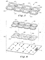
- Figures 1A and 1B illustrate two examples of secondary lenses integrally formed as one component using injection moulding techniques.
- FIG. 1A illustrates an exploded view of a free form lens array assembly 100.
- the assembly 100 comprises a PCB 110 on which are mounted sixteen LED elements 120 arranged as two groups 120A, 120B of eight elements.
- the PCB 110 also includes mounting holes 150, 160 to which a free form lens array 210 is mounted as will be described in more detail below.
- Mounting holes 170 are also provided in the PCB 110 for mounting the assembly 100 to a luminaire housing (not shown), and positioning apertures or holes 180, 190 are provided for the correct alignment of a lens array assembly as will be described in more detail below.
- the assembly 100 also comprises a free form lens array 210 is which can be mounted over either group 120A or group 120B of LED elements 120.
- the free form lens array 210 comprises eight secondary lens elements 220, arranged in a two-by-four configuration, joined together by a skirt portion 230 which surrounds each of the secondary lens elements 220.
- Each secondary lens element 220 comprises a convex portion 220A (shown more clearly in Figure 2 ) formed as part of a first surface and a concave portion 220B (shown in Figure 3 ) formed as part of a second surface respectively of the free form lens array 210.
- a second free form lens array (not shown) may be provided for the other group of LED elements 120.
- the free form lens array 210 is not limited to eight secondary lens elements 220 and may comprise any suitable number of secondary lens elements in accordance with the particular lighting application in which the free form lens array 210 is to be used.
- the alignment and/or orientation of the secondary lens elements 220 within the free form lens array 210 is not limited to the alignment and orientation shown in Figure 1A and described herein and may be any other suitable alignment and/or orientation in accordance with the particular lighting application.
- An alignment pin 240 is formed in the skirt portion 230 of the free form lens array 210 which aligns with a corresponding aperture or hole in a lens holder as will be described in more detail below.
- Other markings may be present on the skirt portion 230 which are intended to provide correct alignment with respect to the PCB 110 and the LED elements 120 of an LED array formed thereon.
- FIG. 1B illustrates an exploded view of a collimator lens array assembly 300.
- the collimator lens assembly comprises PCB 110, described above with reference to Figure 1A , and one collimator lens array 310 which can be mounted over either group 120A or group 120B.
- the collimator lens array 310 comprises eight secondary lens elements 320, arranged in a two-by-four configuration, joined together by an elongate strip 250 extending down the centre of the collimator lens array 310.
- a second collimator lens array (not shown) may be provided over the other group of LED elements 120.
- the collimator lens array 310 is not limited to eight secondary lens elements 320 and may comprise any suitable number of lens elements in accordance with the particular lighting application in which the collimator lens array 310 is to be used.
- the alignment of the secondary lens elements 320 within the collimator lens array 310 is not limited to the alignment shown in Figure 1B and described herein and may be any other suitable alignment in accordance with the particular lighting application.
- the assembly of the secondary lenses on the PCBs needs to be easy and straightforward in an industrial environment.
- a lens holder for mounting the secondary lens array with respect to the PCB.
- the lens holder comprises a simple frame to surround and retain the secondary lens elements, and, in another embodiment, the lens holder comprises a shaped structure to support the secondary lens array as will be described in more detail below.
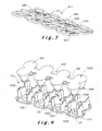
- the lens array assembly 400 comprises the free form lens array 210 shown in Figure 1A and a lens holder 410.
- the lens holder 410 comprises a frame having eight apertures 420 shaped to receive a respective one of the secondary lens elements 220 when assembled.
- the lens holder 410 has a first surface and a second surface, the second surface being in contact with the first surface of the free form lens array 210 when assembled, that is, the lens holder 410 is positioned over the free form lens array 210 and is not in contact with the PCB 110.
- the second surface of the free form lens array 210 is in contact with the PCB 110 when an LED module (as shown in Figure 6 ) is assembled.
- the concave portion 220B of each secondary lens element 220 is placed nearer to the LED element which it is associated than the convex portion 220A.
- the frame includes an aperture or hole 440 with which the alignment pin 240 of the skirt portion 230 of the free form lens array 210 engages when assembled. This ensures correct alignment of the free form lens array 210 with the lens holder 410 so that the secondary lens elements 220 are located within apertures 420 of the lens holder 410, with their convex portions 220A above the frame, when the lens holder 410 is assembled with the free form lens array 210.
- Clips 450, 460 are provided as part of the lens holder 410 for aligning with corresponding apertures or holes 250, 260 formed in the skirt portion 230 of the free form lens array 210 as shown.
- the apertures or holes 250, 260 may comprise elongate slots, but the apertures or holes 250, 260 are not limited to such a configuration.
- the clips 450, 460 extend through the apertures or holes 250, 260 when the frame 410 is assembled with the free form lens array 210 as will be described in more detail below.
- the clips 450, 460 are moulded from the same material as the frame and are integrally formed therewith.
- the clips 450, 460 extend through into corresponding holes 150, 160 formed in the PCB 110.
- Markings 470, 475 on the first surface of the frame 410 are aligned with corresponding markings 270, 275 provided on the first surface of the free form lens array 210, and in particular, on the skirt portion 230 thereof.
- Figure 3 illustrates the lens array assembly 400 from underneath, that is, from the second surface of the free form lens array 210. As shown, the first surface of the free form lens array 210 is in contact with the second surface of the lens holder array 410. Positioning pins 280, 290 are provided on the second surface of the free form lens array 210 which engage with corresponding apertures or holes 180, 190 provided in the PCB 110 (as described above with reference to Figure 1A ).
- the positioning pins 280, 290 are shaped to allow for thermal expansion of an assembled LED module (not shown) without creating any deformation in the free form lens array 210.
- one pin 290 has a circular cross-section and the other pin 280 has a rhomboid (lozenge) cross-section.
- rhomboid lassid
- other cross-sections are possible for the positioning pins 280, 290 as long as they can accommodate dimensional changes due to thermal expansion.
- the positioning pins 280, 290 provide correct referencing of the free form lens array 210 with respect to the PCB 110 when inserted into corresponding apertures 180, 190 in the PCB 110. This reference is maintained between the free form lens array 210 and the PCB 110 with the lens holder 410 being prevented from putting any mechanical constraint on this positioning. In effect, the lens holder 410 is only used to maintain the second surface of the free form lens array 210 in contact with the first surface of the PCB 110.
- the lens holder 410 incorporates clips 450, 460 which provide a simple and rigid mounting of the lens holder 410 to both the free form lens array 210 and the PCB 110.
- the positioning of these clips 450, 460 and their flexibility is crucial to maintain the lens holder 410 properly aligned with respect to the free form lens array 210 and to the PCB 110 whilst adjusting for thermal expansion.
- Figure 4 illustrates a perspective view of the lens holder 410 from underneath so that the location of the clips 450, 460 and the aperture or hole 440 can clearly be seen.
- the clips 450, 460 are flexible and are designed to have sufficient flexibility to adjust with differences in thermal expansion between the material from which the PCB 110 is made and the material from which the lens holder 410 is made.
- materials from which the lens holder 410 may be made include thermoplastic materials, for example, polycarbonate (PC), polyphenylene sulphide (PPS), polybutylene terephthalate (PBT) and polyamide (PA).
- Figure 5 illustrates a top perspective view of the lens array assembly 400.
- the markings 470, 475 and the aperture or hole 440 formed on or in the lens holder 410 are used to ensure that there is correct orientation with the free form lens array 210.
- markings 470, 475 are matched to corresponding markings 270, 275 on the free form lens array 210 as shown in Figure 2 .
- the aperture or hole 440 is sized to accommodate the positioning pin 240 formed on the skirt portion 230 of the free form lens array 210, and is used as a "foolproof" mounting mechanism.
- the provision of the markings 270, 275 and pin 240 on the free form lens array 210 and the markings 470, 475 and aperture or hole 440 on the lens holder 410 ensures that lens holder 410 is correctly oriented with the free form lens array 210 when being assembled. It will readily be appreciated that other methods of ensuring that the free form lens array 210 is correctly oriented with respect to the lens holder 410 are possible, for example, shaped protrusions may be formed on the lens holder which engage corresponding depressions or apertures formed in the skirt portion 230 of the free form lens array 210.
- the clips 450, 460 integrally formed with the frame of the lens holder 410 extend through correspond holes 250, 260 formed in the free form lens array 210 (shown in Figure 2 ), and, when mounted on the PCB 110, the clips 450, 460 extend through corresponding holes 150, 160 (shown in Figure 1A ) to complete a first embodiment of an LED module.
- Figure 6 illustrates an exploded view of such an LED module 500 comprising the PCB 110 and the lens array assembly 400 which comprises the free form lens array 210 and the lens holder 410 as described above.
- the apertures or holes 250, 260 formed in the free form lens array 210 may comprise elongate slots to allow for differences in tolerances when the free form lens array 210 is moulded. These elongate slots also provide compensation for any tolerances in the moulding of the lens holder 410.
- the LED module 500 may include a second lens array assembly which is located alongside the lens array assembly 400 so that both groups 120A, 120B of eight LED elements 120 ( Figures 1A and 1B ) on the PCB 110 are associated with secondary lens elements.
- the lens array assembly may comprise twice the size of the lens array assembly 400 and is capable of being mounted over all of the sixteen secondary lens elements 120.
- the lens holder may comprise four clips instead of two to provide the desired mounting.
- the lens array assembly may comprise one free form lens array having the requisite number of secondary lens elements and two lens holders 410 may be employed to mount the single free form lens array.
- two free form lens arrays may be mounted using a single lens holder.
- the LED module 500 can easily be assembled in seconds without the need for any tools, the clips 450, 460 providing the engagement necessary to retain the components of the LED module together.
- Lens holder 610 comprises a frame having eight apertures 620 shaped to receive a respective one of the lens elements 220 of the free form lens array 210 shown in Figure 2 when assembled.
- the lens holder 610 has a first surface and a second surface, the second surface being in contact with a first surface of the free form lens array 210 when assembled in an identical way to that of the lens holder 410 described above with reference to Figures 2 to 6 .
- the frame includes an aperture or hole (not shown) with which the alignment pin 240 of the skirt portion 230 of the free form lens array 210 engages when assembled. This ensures correct orientation of the free form lens array 210 with the lens holder 610 so that the lens elements 220 are located within apertures 620 of the lens holder 610 when the lens holder 610 is assembled with the free form lens array 210.
- Clips 650, 660 are provided for engaging corresponding holes 250, 260 formed in the skirt portion 230 of the free form lens array 210 as described above.
- the clips 650, 660 extend through the holes 650, 660 when the frame 610 is assembled with the free form lens array 610.
- Markings 670, 675 on the first surface of the frame 610 are aligned with corresponding markings 270, 275 provided on the first surface of the free form lens array 210, and in particular, on the skirt portion 230 thereof.
- secondary lens elements 220 of the free form lens array 210 extend through apertures 620 in the frame so that the convex portion 220A of each secondary lens element is above the frame of the lens holder 610.
- the lens holder 610 further comprises eight louvre elements 695 which are used to prevent backlighting from a luminaire in which an LED module including such a lens holder 610 is mounted. This is advantageous to prevent unwanted illumination of house façades in a residential environment.
- the material of the lens holder 610 may be made from a light absorptive or reflective material depending on the particular properties required for the louvre elements 695.
- the lens holder 610 may be made from the same materials as the lens holder 410 but with a suitable coating to modify the light absorption or reflective properties thereof.
- only one surface of a louvre element may be coated, that is, the surface which is nearer to the secondary lens element 220.
- the lens holder 610 may be of any suitable size in accordance with the particular application of the LED module (not shown) in which it is implemented.
- each secondary lens element has its own positioning pins which engage with corresponding positioning pins on the PCB 110. Whilst it is possible to mount the secondary lens elements separately, this requires more work during assembly to ensure that there is correct alignment with respect to associated LED elements.
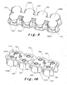
- the lens array assembly 700 comprises a collimator lens array 310 as described with reference to Figure 1B and a lens holder 710.
- the lens holder 710 is positioned between the collimator lens array 310 and the PCB 110 when an LED module (not shown) including such a collimator lens array is assembled.
- the lens holder 710 comprises a frame having first and second surfaces as described above with reference to lens holder 410 ( Figures 2 to 6 ) and lens holder 610 ( Figure 7 ).
- each wall element 725 comprises two concave portions 725A, 725B, and, pairs of wall elements 725 are arranged to oppose one another with pairs of concave portions in defining the recesses 720.
- Each concave portion 725A, 725B includes a clip 725C which cooperates with a clip of an opposed concave portion to engage a secondary lens element 320 of the collimator lens array 310 as will be described in more detail below.
- Each recess 720 has a proximal end 720A and a distal end 720B, the proximal end 720A being located adjacent the frame and the distal end 720B being spaced from the frame.
- the distance between the proximal end 720A and the distal end 720B of a recess is substantially the same as the height of each secondary lens element 320 of the collimator lens array 310.
- a circular aperture 720C is provided in the frame so that the frame can be positioned on the PCB 110 ( Figure 1B ) with the LED elements 120 mounted on the PCB 110 being aligned with the circular apertures 720C.
- each secondary lens element 320 of the collimator lens array 310 is substantially conical with a proximal end 320A and a distal end 320B, the distal end 320B having a larger cross section than the proximal end 320A.
- the proximal end 320A and the distal end 320B of each secondary lens element 320 is respectively aligned with the proximal end 720A and the distal end 720B of each recess 720.
- each secondary lens element 320 is centred within the recess 720 with respect to the circular aperture 720C associated therewith, and, the distal end 320C is retained in position within the recess 720 by clips 725C of the opposing concave portions of the two wall elements 725 defining the recess 720. This will be described in more detail below with reference to Figures 9 and 10 .
- FIG. 9 illustrates a perspective view of the lens array assembly 700. As shown, each secondary lens element 320 is retained within one recess 720 with the proximal portion 320A being located in the circular aperture 720C and the clips 725C of the wall elements 725 surrounding a portion of the distal end 320B of the secondary lens element 320.
- clips 750, 760 are provided which correspond to the clips 450, 460 of the lens holder 410 and the clips 650, 660 of the lens holder 610.
- the clips 750, 760 do not extend through the collimator lens array 310 when the collimator lens array 310 is assembled in the lens holder 710.
- Alignment pins 780, 790 are provided for engaging respective apertures or holes 180, 190 in the PCB 110.
- the alignment pins 780, 790 take the place of the positioning pins 280, 290 of the free form lens array 210 ( Figure 3 ) to ensure that there is alignment of the lens holder 710 with respect to the LED elements 120 on the PCB 110.
- the positioning pins 780, 790 located on the lens holder 710.
- the positioning pins may have the same or different cross-sections to allow for changes due to thermal expansion of an assembled LED module (not shown) without creating deformation in the collimator lens array 310 or the lens holder 710.
- positioning pin 780 has a rhomboid (lozenge) cross section
- positioning pin 790 has a circular cross-section.
- any cross-section combination is possible as long as the positioning pin can accommodate thermal expansion.
- the collimator lens array 310 may comprise secondary lens elements 320 which are arranged in a different format within the array and connected together in a different manner.
- the free form lens array and the collimator lens array are moulded in a single process so that the secondary lens elements are connected to one another to provide easy of handling during assembly of the lens arrays and then the final LED module.
- the luminaires can be operated at higher currents to provide more luminous flux in the same luminaire housing (as is the case for existing designs), or, for a given luminous flux, the required heat dissipation capacity can be reduced with an accompanying material cost saving (as would be the case for new designs).
Priority Applications (19)
| Application Number | Priority Date | Filing Date | Title |
|---|---|---|---|
| HUE15152505A HUE034537T2 (en) | 2015-01-26 | 2015-01-26 | Innovations within or around lens blocks |
| EP15152505.2A EP2966346B1 (de) | 2015-01-26 | 2015-01-26 | Verbesserungen an oder im Zusammenhang mit Linsenanordnungen |
| PT151525052T PT2966346T (pt) | 2015-01-26 | 2015-01-26 | Melhorias em arranjos matriciais de lentes ou relacionadas com arranjos matriciais de lentes |
| DK15152505.2T DK2966346T3 (en) | 2015-01-26 | 2015-01-26 | Improvements in or related to lens devices |
| TR2017/08742T TR201708742T4 (tr) | 2015-01-26 | 2015-01-26 | Mercek dizilerinde veya mercek dizileriyle ilgili iyileştirmeler. |
| PL15152505T PL2966346T3 (pl) | 2015-01-26 | 2015-01-26 | Ulepszenia w lub odnoszące się do soczewkowych układów |
| ES15152505.2T ES2628866T3 (es) | 2015-01-26 | 2015-01-26 | Mejoras en, o relacionadas con, agrupaciones de lentes |
| RS20170585A RS56061B1 (sr) | 2015-01-26 | 2015-01-26 | Poboljšanja u ili koja se odnose na nizove sočiva |
| SG10201509775SA SG10201509775SA (en) | 2015-01-26 | 2015-11-27 | Improvements in or relating to lens arrays |
| CA2913679A CA2913679C (en) | 2015-01-26 | 2015-11-30 | Improvements in or relating to lens arrays |
| AU2015264865A AU2015264865B2 (en) | 2015-01-26 | 2015-12-03 | Improvements in or relating to lens arrays |
| PE2015002592A PE20160929A1 (es) | 2015-01-26 | 2015-12-10 | Mejoras en o relacionadas con conjuntos de lentes |
| CL2015003607A CL2015003607A1 (es) | 2015-01-26 | 2015-12-11 | Mejoras en o relacionadas con conjuntos de lentes |
| ZA2015/09159A ZA201509159B (en) | 2015-01-26 | 2015-12-15 | Improvements in or relating to lens arrays |
| BR102015031513A BR102015031513A2 (pt) | 2015-01-26 | 2015-12-16 | aprimoramentos em/ou relacionados a arranjos de lente |
| CN201510958582.9A CN105823007B (zh) | 2015-01-26 | 2015-12-18 | 透镜阵列中的或者与透镜阵列相关的改进 |
| US14/975,069 US9939125B2 (en) | 2015-01-26 | 2015-12-18 | Lens arrays and mountings |
| KR1020150181568A KR20160091812A (ko) | 2015-01-26 | 2015-12-18 | 렌즈 어레이 |
| US15/907,145 US10197242B2 (en) | 2015-01-26 | 2018-02-27 | Lens arrays and mountings |
Applications Claiming Priority (1)
| Application Number | Priority Date | Filing Date | Title |
|---|---|---|---|
| EP15152505.2A EP2966346B1 (de) | 2015-01-26 | 2015-01-26 | Verbesserungen an oder im Zusammenhang mit Linsenanordnungen |
Publications (2)
| Publication Number | Publication Date |
|---|---|
| EP2966346A1 true EP2966346A1 (de) | 2016-01-13 |
| EP2966346B1 EP2966346B1 (de) | 2017-04-19 |
Family
ID=52462134
Family Applications (1)
| Application Number | Title | Priority Date | Filing Date |
|---|---|---|---|
| EP15152505.2A Active EP2966346B1 (de) | 2015-01-26 | 2015-01-26 | Verbesserungen an oder im Zusammenhang mit Linsenanordnungen |
Country Status (18)
| Country | Link |
|---|---|
| US (2) | US9939125B2 (de) |
| EP (1) | EP2966346B1 (de) |
| KR (1) | KR20160091812A (de) |
| CN (1) | CN105823007B (de) |
| AU (1) | AU2015264865B2 (de) |
| BR (1) | BR102015031513A2 (de) |
| CA (1) | CA2913679C (de) |
| CL (1) | CL2015003607A1 (de) |
| DK (1) | DK2966346T3 (de) |
| ES (1) | ES2628866T3 (de) |
| HU (1) | HUE034537T2 (de) |
| PE (1) | PE20160929A1 (de) |
| PL (1) | PL2966346T3 (de) |
| PT (1) | PT2966346T (de) |
| RS (1) | RS56061B1 (de) |
| SG (1) | SG10201509775SA (de) |
| TR (1) | TR201708742T4 (de) |
| ZA (1) | ZA201509159B (de) |
Cited By (9)
| Publication number | Priority date | Publication date | Assignee | Title |
|---|---|---|---|---|
| DE202017105600U1 (de) | 2017-09-15 | 2018-12-18 | Rp-Technik Gmbh | Linsenhalter, insbesondere für eine Kombinationslinse einer Beleuchtungsoptik, sowie Leuchte mit einem entsprechenden Linsenhalter |
| WO2019134875A1 (en) | 2018-01-05 | 2019-07-11 | Schreder Sa | Moveable lens luminaire |
| US10655822B2 (en) | 2016-08-09 | 2020-05-19 | Signify Holding B.V. | Configurable optical module and LED assembly |
| WO2020249684A1 (en) * | 2019-06-12 | 2020-12-17 | Schreder S.A. | Light emitting device with adaptable glare class |
| WO2021224370A1 (en) * | 2020-05-08 | 2021-11-11 | Signify Holding B.V. | A lighting unit and a luminaire |
| WO2022194568A1 (en) * | 2021-03-18 | 2022-09-22 | Signify Holding B.V. | Optical component for a luminaire |
| EP4215954A1 (de) * | 2022-01-21 | 2023-07-26 | Leuze electronic GmbH + Co. KG | Optischer sensor |
| EP4050668A4 (de) * | 2019-10-25 | 2024-01-10 | Seoul Semiconductor Shenzhen Co Ltd | Linsenmodul |
| WO2024013397A1 (en) | 2022-07-15 | 2024-01-18 | Schreder S.A. | Modular luminaire head |
Families Citing this family (29)
| Publication number | Priority date | Publication date | Assignee | Title |
|---|---|---|---|---|
| US10292784B2 (en) * | 2010-12-10 | 2019-05-21 | Illumix Surgical Canada Inc. | Illuminating surgical device |
| CN112483911B (zh) | 2015-05-20 | 2023-02-21 | 日亚化学工业株式会社 | 发光装置 |
| US10816165B2 (en) * | 2015-11-19 | 2020-10-27 | Lsi Industries, Inc. | LED luminaire assembly |
| CN108779905B (zh) * | 2016-01-26 | 2021-08-20 | 新加坡恒立私人有限公司 | 多模式照明模块和相关方法 |
| US10184639B2 (en) * | 2016-07-05 | 2019-01-22 | JST Performance, LLC | Method and apparatus for subtending light |
| KR102623546B1 (ko) * | 2016-09-23 | 2024-01-10 | 삼성전자주식회사 | 조명용 렌즈, 조명용 렌즈 어레이 및 이를 포함하는 조명 장치 |
| FR3056699B1 (fr) | 2016-09-26 | 2019-06-28 | Valeo Vision | Module lumineux et dispositif lumineux pour vehicule auto-mobile comportant un tel module lumineux |
| US20180286295A1 (en) * | 2017-03-28 | 2018-10-04 | GE Lighting Solutions, LLC | Light emitting diode assembly |
| KR101942315B1 (ko) * | 2017-04-06 | 2019-01-31 | 주식회사 나스필코리아 | 엘이디모듈을 구성하는 엘이디칩의 광확산렌즈용 홀더 |
| WO2018202280A1 (en) * | 2017-05-02 | 2018-11-08 | Osram Opto Semiconductors Gmbh | Production of a chip module |
| KR20200010348A (ko) | 2017-05-18 | 2020-01-30 | 루미리즈 홀딩 비.브이. | 높은 방사조도를 갖는 조명 어셈블리 |
| US10378732B2 (en) * | 2017-06-06 | 2019-08-13 | Musco Corporation | Apparatus, method, and system for precise LED lighting |
| USD859731S1 (en) * | 2017-08-22 | 2019-09-10 | Opple Lighting Co., Ltd. | Light |
| CN107450149A (zh) * | 2017-08-31 | 2017-12-08 | 赣州光联电子科技有限公司 | 一种透镜安装固定装置及安装固定方法 |
| CN108563074B (zh) * | 2018-06-04 | 2022-04-05 | 东莞广辰光电科技有限公司 | 一种具方向性的薄型液晶显示器背光照明系统 |
| US10895364B2 (en) * | 2018-11-13 | 2021-01-19 | Abl Ip Holding Llc | Energy reduction optics |
| CN209012945U (zh) * | 2018-12-17 | 2019-06-21 | 欧普照明股份有限公司 | 照明灯具 |
| JP6803415B2 (ja) * | 2019-01-30 | 2020-12-23 | Hoya株式会社 | 回路基板固定構造、及びこれを備える光照射装置 |
| CN114270092A (zh) | 2019-05-10 | 2022-04-01 | 合保照明公司 | 用于led照明器具的透镜组件 |
| EP3738889A1 (de) * | 2019-05-17 | 2020-11-18 | Goodrich Lighting Systems GmbH | Beleuchtungsvorrichtung, flugzeug mit einer derartigen beleuchtungsvorrichtung und verfahren zur herstellung einer beleuchtungsvorrichtung |
| EP3805833A1 (de) * | 2019-10-09 | 2021-04-14 | Lumileds Holding B.V. | Beleuchtungsvorrichtung und verfahren zur herstellung einer beleuchtungsvorrichtung |
| CN210717380U (zh) * | 2019-11-08 | 2020-06-09 | 欧普照明股份有限公司 | 透镜及光源模组 |
| WO2021249979A1 (en) * | 2020-06-11 | 2021-12-16 | Signify Holding B.V. | Lens plate |
| GB2599354A (en) | 2020-09-08 | 2022-04-06 | Iq Structures Sro | Optical cells for modular luminaires |
| GB2599076A (en) | 2020-09-08 | 2022-03-30 | Iq Structures Sro | Modular luminaires |
| DE102021106644B4 (de) | 2021-03-18 | 2023-11-16 | Bjb Gmbh & Co. Kg | Abdeckung für ein Leuchtmittel sowie Leuchte mit Abdeckung |
| US11499689B1 (en) * | 2021-06-28 | 2022-11-15 | Valeo North America, Inc. | Light system including a plurality of printed circuit boards having multiple functions |
| KR102546988B1 (ko) * | 2021-06-30 | 2023-06-22 | 엘지전자 주식회사 | 디스플레이 디바이스 |
| NL2029021B1 (en) | 2021-08-23 | 2023-03-03 | Schreder Sa | Optical plate with integrated connection |
Citations (8)
| Publication number | Priority date | Publication date | Assignee | Title |
|---|---|---|---|---|
| US20080043466A1 (en) * | 2006-08-16 | 2008-02-21 | Chakmakjian Stephen H | Illumination devices |
| US20110103051A1 (en) * | 2009-10-30 | 2011-05-05 | Ruud Lighting, Inc. | Led apparatus and method for accurate lens alignment |
| US20110280014A1 (en) * | 2009-07-23 | 2011-11-17 | Fraen Corporation | Devices and methods for area lighting |
| DE202012003680U1 (de) * | 2012-04-13 | 2012-05-18 | Gratz Luminance GmbH | LED-Leuchte |
| US20120268930A1 (en) * | 2011-04-25 | 2012-10-25 | Cree, Inc. | Optical arrangement for a solid-state lamp |
| US20130058088A1 (en) * | 2011-09-06 | 2013-03-07 | Asia Vital Components Co., Ltd. | Led lighting structure |
| WO2013142437A1 (en) * | 2012-03-18 | 2013-09-26 | Robe Lighting, Inc. | Improved collimation system for an led luminaire |
| US20140268761A1 (en) * | 2009-10-30 | 2014-09-18 | Cree, Inc. | One-Piece Multi-Lens Optical Member and Method of Manufacture |
Family Cites Families (11)
| Publication number | Priority date | Publication date | Assignee | Title |
|---|---|---|---|---|
| US20050083696A1 (en) * | 2003-10-20 | 2005-04-21 | Po-Liang Chiang | Structure of LED illuminating apparatus |
| US20060279626A1 (en) * | 2005-06-10 | 2006-12-14 | Tu Shun L | Optics lens structure of LED printer head |
| US8405015B1 (en) * | 2009-03-30 | 2013-03-26 | Eric Klein | Multi-image led projector for sequentially projecting a series of transparency images onto a screen |
| US20100284089A1 (en) * | 2009-05-07 | 2010-11-11 | San-Woei Shyu | Stacked optical glass lens array, stacked lens module and manufacturing method thereof |
| US20120300456A1 (en) * | 2011-05-26 | 2012-11-29 | Phillips Iii William E | Reflectors optimized for led lighting fixture |
| JP5789499B2 (ja) * | 2011-11-25 | 2015-10-07 | 株式会社沖データ | レンズアレイ、レンズユニット、ledヘッド、露光装置、画像形成装置及び読取装置 |
| CN202956522U (zh) * | 2012-04-28 | 2013-05-29 | 欧司朗股份有限公司 | 透镜单元及具有该透镜单元的照明装置 |
| US8974077B2 (en) * | 2012-07-30 | 2015-03-10 | Ultravision Technologies, Llc | Heat sink for LED light source |
| US9464778B2 (en) * | 2014-01-21 | 2016-10-11 | Cree, Inc. | Lighting device utilizing a double fresnel lens |
| US9625119B2 (en) * | 2014-07-31 | 2017-04-18 | Excelitas Canada, Inc. | Non-uniform lens array for illumination profile modification |
| KR20160019601A (ko) * | 2014-08-11 | 2016-02-22 | 삼성디스플레이 주식회사 | 백라이트 유닛 및 이를 포함하는 표시 장치 |
-
2015
- 2015-01-26 EP EP15152505.2A patent/EP2966346B1/de active Active
- 2015-01-26 ES ES15152505.2T patent/ES2628866T3/es active Active
- 2015-01-26 RS RS20170585A patent/RS56061B1/sr unknown
- 2015-01-26 DK DK15152505.2T patent/DK2966346T3/en active
- 2015-01-26 PT PT151525052T patent/PT2966346T/pt unknown
- 2015-01-26 HU HUE15152505A patent/HUE034537T2/en unknown
- 2015-01-26 PL PL15152505T patent/PL2966346T3/pl unknown
- 2015-01-26 TR TR2017/08742T patent/TR201708742T4/tr unknown
- 2015-11-27 SG SG10201509775SA patent/SG10201509775SA/en unknown
- 2015-11-30 CA CA2913679A patent/CA2913679C/en active Active
- 2015-12-03 AU AU2015264865A patent/AU2015264865B2/en active Active
- 2015-12-10 PE PE2015002592A patent/PE20160929A1/es not_active Application Discontinuation
- 2015-12-11 CL CL2015003607A patent/CL2015003607A1/es unknown
- 2015-12-15 ZA ZA2015/09159A patent/ZA201509159B/en unknown
- 2015-12-16 BR BR102015031513A patent/BR102015031513A2/pt not_active Application Discontinuation
- 2015-12-18 CN CN201510958582.9A patent/CN105823007B/zh not_active Expired - Fee Related
- 2015-12-18 KR KR1020150181568A patent/KR20160091812A/ko unknown
- 2015-12-18 US US14/975,069 patent/US9939125B2/en active Active
-
2018
- 2018-02-27 US US15/907,145 patent/US10197242B2/en active Active
Patent Citations (8)
| Publication number | Priority date | Publication date | Assignee | Title |
|---|---|---|---|---|
| US20080043466A1 (en) * | 2006-08-16 | 2008-02-21 | Chakmakjian Stephen H | Illumination devices |
| US20110280014A1 (en) * | 2009-07-23 | 2011-11-17 | Fraen Corporation | Devices and methods for area lighting |
| US20110103051A1 (en) * | 2009-10-30 | 2011-05-05 | Ruud Lighting, Inc. | Led apparatus and method for accurate lens alignment |
| US20140268761A1 (en) * | 2009-10-30 | 2014-09-18 | Cree, Inc. | One-Piece Multi-Lens Optical Member and Method of Manufacture |
| US20120268930A1 (en) * | 2011-04-25 | 2012-10-25 | Cree, Inc. | Optical arrangement for a solid-state lamp |
| US20130058088A1 (en) * | 2011-09-06 | 2013-03-07 | Asia Vital Components Co., Ltd. | Led lighting structure |
| WO2013142437A1 (en) * | 2012-03-18 | 2013-09-26 | Robe Lighting, Inc. | Improved collimation system for an led luminaire |
| DE202012003680U1 (de) * | 2012-04-13 | 2012-05-18 | Gratz Luminance GmbH | LED-Leuchte |
Cited By (12)
| Publication number | Priority date | Publication date | Assignee | Title |
|---|---|---|---|---|
| US10655822B2 (en) | 2016-08-09 | 2020-05-19 | Signify Holding B.V. | Configurable optical module and LED assembly |
| DE202017105600U1 (de) | 2017-09-15 | 2018-12-18 | Rp-Technik Gmbh | Linsenhalter, insbesondere für eine Kombinationslinse einer Beleuchtungsoptik, sowie Leuchte mit einem entsprechenden Linsenhalter |
| WO2019134875A1 (en) | 2018-01-05 | 2019-07-11 | Schreder Sa | Moveable lens luminaire |
| WO2020249684A1 (en) * | 2019-06-12 | 2020-12-17 | Schreder S.A. | Light emitting device with adaptable glare class |
| NL2023295B1 (en) * | 2019-06-12 | 2021-01-21 | Schreder Sa | Light emitting device with adaptable glare class |
| EP4050668A4 (de) * | 2019-10-25 | 2024-01-10 | Seoul Semiconductor Shenzhen Co Ltd | Linsenmodul |
| WO2021224370A1 (en) * | 2020-05-08 | 2021-11-11 | Signify Holding B.V. | A lighting unit and a luminaire |
| US11781730B2 (en) | 2020-05-08 | 2023-10-10 | Signify Holding, B.V. | Lighting unit and luminaire |
| WO2022194568A1 (en) * | 2021-03-18 | 2022-09-22 | Signify Holding B.V. | Optical component for a luminaire |
| EP4215954A1 (de) * | 2022-01-21 | 2023-07-26 | Leuze electronic GmbH + Co. KG | Optischer sensor |
| WO2024013397A1 (en) | 2022-07-15 | 2024-01-18 | Schreder S.A. | Modular luminaire head |
| NL2032515B1 (en) | 2022-07-15 | 2024-01-25 | Schreder Sa | Modular luminaire head |
Also Published As
| Publication number | Publication date |
|---|---|
| KR20160091812A (ko) | 2016-08-03 |
| ZA201509159B (en) | 2016-11-30 |
| BR102015031513A2 (pt) | 2017-02-21 |
| DK2966346T3 (en) | 2017-07-03 |
| CN105823007A (zh) | 2016-08-03 |
| TR201708742T4 (tr) | 2018-11-21 |
| ES2628866T3 (es) | 2017-08-04 |
| AU2015264865A1 (en) | 2016-08-11 |
| AU2015264865B2 (en) | 2021-05-27 |
| US20180187862A1 (en) | 2018-07-05 |
| CA2913679C (en) | 2023-10-31 |
| US20160215955A1 (en) | 2016-07-28 |
| HUE034537T2 (en) | 2018-02-28 |
| PL2966346T3 (pl) | 2017-09-29 |
| CA2913679A1 (en) | 2016-07-26 |
| SG10201509775SA (en) | 2016-08-30 |
| US10197242B2 (en) | 2019-02-05 |
| CL2015003607A1 (es) | 2016-08-05 |
| CN105823007B (zh) | 2020-01-14 |
| PT2966346T (pt) | 2017-06-29 |
| US9939125B2 (en) | 2018-04-10 |
| EP2966346B1 (de) | 2017-04-19 |
| RS56061B1 (sr) | 2017-10-31 |
| PE20160929A1 (es) | 2016-09-14 |
Similar Documents
| Publication | Publication Date | Title |
|---|---|---|
| US10197242B2 (en) | Lens arrays and mountings | |
| EP2494266B1 (de) | Led-vorrichtung und verfahren für genaue linsenausrichtung | |
| US9028097B2 (en) | LED apparatus and method for accurate lens alignment | |
| US8919991B2 (en) | Tube-type LED illumination lamp | |
| JP6450891B1 (ja) | 照明装置の熱感度の低減 | |
| WO2013028965A2 (en) | Circuit board mount for led light | |
| US20120069568A1 (en) | Lighting module and corresponding method | |
| US10502370B2 (en) | Semiconductor lamp | |
| MX2015002314A (es) | Modulo de iluminacion para un vehiculo motorizado. | |
| CN109790970B (zh) | 可配置的光学模块和led组件 | |
| US9797565B2 (en) | LED engine for emergency lighting | |
| US10663135B2 (en) | Light module for a vehicle headlight | |
| EP2587133B1 (de) | Beleuchtungskomponente mit led-reflektorstreifen | |
| CN112867892A (zh) | 照明系统 | |
| BE1023833B1 (fr) | Ameliorations de reseaux de lentilles ou en relation avec ceux-ci | |
| AU2013205063B2 (en) | LED apparatus and method for accurate lens alignment | |
| JP2014235854A (ja) | 直管形ledランプ及び照明装置 |
Legal Events
| Date | Code | Title | Description |
|---|---|---|---|
| PUAI | Public reference made under article 153(3) epc to a published international application that has entered the european phase |
Free format text: ORIGINAL CODE: 0009012 |
|
| 17P | Request for examination filed |
Effective date: 20151125 |
|
| AK | Designated contracting states |
Kind code of ref document: A1 Designated state(s): AL AT BE BG CH CY CZ DE DK EE ES FI FR GB GR HR HU IE IS IT LI LT LU LV MC MK MT NL NO PL PT RO RS SE SI SK SM TR |
|
| AX | Request for extension of the european patent |
Extension state: BA ME |
|
| 17Q | First examination report despatched |
Effective date: 20160408 |
|
| RIC1 | Information provided on ipc code assigned before grant |
Ipc: F21W 131/103 20060101ALN20160728BHEP Ipc: F21V 17/00 20060101ALI20160728BHEP Ipc: G02B 19/00 20060101ALI20160728BHEP Ipc: F21Y 115/10 20160101ALN20160728BHEP Ipc: F21Y 105/10 20160101ALN20160728BHEP Ipc: F21V 5/00 20150101AFI20160728BHEP Ipc: G02B 3/00 20060101ALI20160728BHEP Ipc: F21V 5/04 20060101ALI20160728BHEP |
|
| GRAP | Despatch of communication of intention to grant a patent |
Free format text: ORIGINAL CODE: EPIDOSNIGR1 |
|
| STAA | Information on the status of an ep patent application or granted ep patent |
Free format text: STATUS: GRANT OF PATENT IS INTENDED |
|
| RIC1 | Information provided on ipc code assigned before grant |
Ipc: F21W 131/103 20060101ALN20161107BHEP Ipc: F21V 5/00 20150101AFI20161107BHEP Ipc: F21Y 115/10 20160101ALN20161107BHEP Ipc: F21V 17/00 20060101ALI20161107BHEP Ipc: G02B 3/00 20060101ALI20161107BHEP Ipc: G02B 19/00 20060101ALI20161107BHEP Ipc: F21V 5/04 20060101ALI20161107BHEP Ipc: F21Y 105/10 20160101ALN20161107BHEP |
|
| INTG | Intention to grant announced |
Effective date: 20161121 |
|
| GRAS | Grant fee paid |
Free format text: ORIGINAL CODE: EPIDOSNIGR3 |
|
| GRAA | (expected) grant |
Free format text: ORIGINAL CODE: 0009210 |
|
| STAA | Information on the status of an ep patent application or granted ep patent |
Free format text: STATUS: THE PATENT HAS BEEN GRANTED |
|
| AK | Designated contracting states |
Kind code of ref document: B1 Designated state(s): AL AT BE BG CH CY CZ DE DK EE ES FI FR GB GR HR HU IE IS IT LI LT LU LV MC MK MT NL NO PL PT RO RS SE SI SK SM TR |
|
| REG | Reference to a national code |
Ref country code: GB Ref legal event code: FG4D |
|
| REG | Reference to a national code |
Ref country code: CH Ref legal event code: EP |
|
| REG | Reference to a national code |
Ref country code: AT Ref legal event code: REF Ref document number: 886334 Country of ref document: AT Kind code of ref document: T Effective date: 20170515 |
|
| REG | Reference to a national code |
Ref country code: IE Ref legal event code: FG4D |
|
| REG | Reference to a national code |
Ref country code: DE Ref legal event code: R096 Ref document number: 602015002268 Country of ref document: DE |
|
| REG | Reference to a national code |
Ref country code: CH Ref legal event code: NV Representative=s name: GEVERS SA, CH |
|
| REG | Reference to a national code |
Ref country code: SE Ref legal event code: TRGR |
|
| REG | Reference to a national code |
Ref country code: NL Ref legal event code: FP |
|
| REG | Reference to a national code |
Ref country code: PT Ref legal event code: SC4A Ref document number: 2966346 Country of ref document: PT Date of ref document: 20170629 Kind code of ref document: T Free format text: AVAILABILITY OF NATIONAL TRANSLATION Effective date: 20170619 |
|
| REG | Reference to a national code |
Ref country code: DK Ref legal event code: T3 Effective date: 20170702 |
|
| REG | Reference to a national code |
Ref country code: ES Ref legal event code: FG2A Ref document number: 2628866 Country of ref document: ES Kind code of ref document: T3 Effective date: 20170804 |
|
| REG | Reference to a national code |
Ref country code: NO Ref legal event code: T2 Effective date: 20170419 |
|
| REG | Reference to a national code |
Ref country code: LT Ref legal event code: MG4D |
|
| PG25 | Lapsed in a contracting state [announced via postgrant information from national office to epo] |
Ref country code: GR Free format text: LAPSE BECAUSE OF FAILURE TO SUBMIT A TRANSLATION OF THE DESCRIPTION OR TO PAY THE FEE WITHIN THE PRESCRIBED TIME-LIMIT Effective date: 20170720 Ref country code: LT Free format text: LAPSE BECAUSE OF FAILURE TO SUBMIT A TRANSLATION OF THE DESCRIPTION OR TO PAY THE FEE WITHIN THE PRESCRIBED TIME-LIMIT Effective date: 20170419 Ref country code: HR Free format text: LAPSE BECAUSE OF FAILURE TO SUBMIT A TRANSLATION OF THE DESCRIPTION OR TO PAY THE FEE WITHIN THE PRESCRIBED TIME-LIMIT Effective date: 20170419 |
|
| PG25 | Lapsed in a contracting state [announced via postgrant information from national office to epo] |
Ref country code: LV Free format text: LAPSE BECAUSE OF FAILURE TO SUBMIT A TRANSLATION OF THE DESCRIPTION OR TO PAY THE FEE WITHIN THE PRESCRIBED TIME-LIMIT Effective date: 20170419 Ref country code: BG Free format text: LAPSE BECAUSE OF FAILURE TO SUBMIT A TRANSLATION OF THE DESCRIPTION OR TO PAY THE FEE WITHIN THE PRESCRIBED TIME-LIMIT Effective date: 20170719 Ref country code: IS Free format text: LAPSE BECAUSE OF FAILURE TO SUBMIT A TRANSLATION OF THE DESCRIPTION OR TO PAY THE FEE WITHIN THE PRESCRIBED TIME-LIMIT Effective date: 20170819 |
|
| REG | Reference to a national code |
Ref country code: FR Ref legal event code: PLFP Year of fee payment: 4 |
|
| REG | Reference to a national code |
Ref country code: DE Ref legal event code: R097 Ref document number: 602015002268 Country of ref document: DE |
|
| PG25 | Lapsed in a contracting state [announced via postgrant information from national office to epo] |
Ref country code: RO Free format text: LAPSE BECAUSE OF FAILURE TO SUBMIT A TRANSLATION OF THE DESCRIPTION OR TO PAY THE FEE WITHIN THE PRESCRIBED TIME-LIMIT Effective date: 20170419 Ref country code: SK Free format text: LAPSE BECAUSE OF FAILURE TO SUBMIT A TRANSLATION OF THE DESCRIPTION OR TO PAY THE FEE WITHIN THE PRESCRIBED TIME-LIMIT Effective date: 20170419 Ref country code: CZ Free format text: LAPSE BECAUSE OF FAILURE TO SUBMIT A TRANSLATION OF THE DESCRIPTION OR TO PAY THE FEE WITHIN THE PRESCRIBED TIME-LIMIT Effective date: 20170419 Ref country code: EE Free format text: LAPSE BECAUSE OF FAILURE TO SUBMIT A TRANSLATION OF THE DESCRIPTION OR TO PAY THE FEE WITHIN THE PRESCRIBED TIME-LIMIT Effective date: 20170419 |
|
| PLBE | No opposition filed within time limit |
Free format text: ORIGINAL CODE: 0009261 |
|
| STAA | Information on the status of an ep patent application or granted ep patent |
Free format text: STATUS: NO OPPOSITION FILED WITHIN TIME LIMIT |
|
| PG25 | Lapsed in a contracting state [announced via postgrant information from national office to epo] |
Ref country code: SM Free format text: LAPSE BECAUSE OF FAILURE TO SUBMIT A TRANSLATION OF THE DESCRIPTION OR TO PAY THE FEE WITHIN THE PRESCRIBED TIME-LIMIT Effective date: 20170419 |
|
| REG | Reference to a national code |
Ref country code: HU Ref legal event code: AG4A Ref document number: E034537 Country of ref document: HU |
|
| 26N | No opposition filed |
Effective date: 20180122 |
|
| PG25 | Lapsed in a contracting state [announced via postgrant information from national office to epo] |
Ref country code: SI Free format text: LAPSE BECAUSE OF FAILURE TO SUBMIT A TRANSLATION OF THE DESCRIPTION OR TO PAY THE FEE WITHIN THE PRESCRIBED TIME-LIMIT Effective date: 20170419 |
|
| REG | Reference to a national code |
Ref country code: IE Ref legal event code: MM4A |
|
| PG25 | Lapsed in a contracting state [announced via postgrant information from national office to epo] |
Ref country code: IE Free format text: LAPSE BECAUSE OF NON-PAYMENT OF DUE FEES Effective date: 20180126 |
|
| REG | Reference to a national code |
Ref country code: CH Ref legal event code: NV Representative=s name: BOVARD SA NEUCHATEL CONSEILS EN PROPRIETE INTE, CH |
|
| PG25 | Lapsed in a contracting state [announced via postgrant information from national office to epo] |
Ref country code: MC Free format text: LAPSE BECAUSE OF FAILURE TO SUBMIT A TRANSLATION OF THE DESCRIPTION OR TO PAY THE FEE WITHIN THE PRESCRIBED TIME-LIMIT Effective date: 20170419 |
|
| PG25 | Lapsed in a contracting state [announced via postgrant information from national office to epo] |
Ref country code: MT Free format text: LAPSE BECAUSE OF NON-PAYMENT OF DUE FEES Effective date: 20180126 |
|
| PGFP | Annual fee paid to national office [announced via postgrant information from national office to epo] |
Ref country code: SE Payment date: 20200128 Year of fee payment: 6 Ref country code: AT Payment date: 20200123 Year of fee payment: 6 Ref country code: HU Payment date: 20200120 Year of fee payment: 6 Ref country code: NO Payment date: 20200123 Year of fee payment: 6 Ref country code: FI Payment date: 20200121 Year of fee payment: 6 Ref country code: DK Payment date: 20200127 Year of fee payment: 6 |
|
| PGFP | Annual fee paid to national office [announced via postgrant information from national office to epo] |
Ref country code: LU Payment date: 20200128 Year of fee payment: 6 Ref country code: RS Payment date: 20200106 Year of fee payment: 6 Ref country code: CH Payment date: 20200127 Year of fee payment: 6 |
|
| PG25 | Lapsed in a contracting state [announced via postgrant information from national office to epo] |
Ref country code: MK Free format text: LAPSE BECAUSE OF NON-PAYMENT OF DUE FEES Effective date: 20170419 Ref country code: CY Free format text: LAPSE BECAUSE OF FAILURE TO SUBMIT A TRANSLATION OF THE DESCRIPTION OR TO PAY THE FEE WITHIN THE PRESCRIBED TIME-LIMIT Effective date: 20170419 |
|
| PGFP | Annual fee paid to national office [announced via postgrant information from national office to epo] |
Ref country code: TR Payment date: 20200122 Year of fee payment: 6 |
|
| PG25 | Lapsed in a contracting state [announced via postgrant information from national office to epo] |
Ref country code: AL Free format text: LAPSE BECAUSE OF FAILURE TO SUBMIT A TRANSLATION OF THE DESCRIPTION OR TO PAY THE FEE WITHIN THE PRESCRIBED TIME-LIMIT Effective date: 20170419 |
|
| REG | Reference to a national code |
Ref country code: FI Ref legal event code: MAE |
|
| REG | Reference to a national code |
Ref country code: DK Ref legal event code: EBP Effective date: 20210131 |
|
| REG | Reference to a national code |
Ref country code: NO Ref legal event code: MMEP |
|
| REG | Reference to a national code |
Ref country code: CH Ref legal event code: PL Ref country code: SE Ref legal event code: EUG |
|
| REG | Reference to a national code |
Ref country code: AT Ref legal event code: MM01 Ref document number: 886334 Country of ref document: AT Kind code of ref document: T Effective date: 20210126 |
|
| PG25 | Lapsed in a contracting state [announced via postgrant information from national office to epo] |
Ref country code: LU Free format text: LAPSE BECAUSE OF NON-PAYMENT OF DUE FEES Effective date: 20210126 |
|
| PG25 | Lapsed in a contracting state [announced via postgrant information from national office to epo] |
Ref country code: AT Free format text: LAPSE BECAUSE OF NON-PAYMENT OF DUE FEES Effective date: 20210126 Ref country code: FI Free format text: LAPSE BECAUSE OF NON-PAYMENT OF DUE FEES Effective date: 20210126 Ref country code: HU Free format text: LAPSE BECAUSE OF NON-PAYMENT OF DUE FEES Effective date: 20210127 |
|
| PG25 | Lapsed in a contracting state [announced via postgrant information from national office to epo] |
Ref country code: LI Free format text: LAPSE BECAUSE OF NON-PAYMENT OF DUE FEES Effective date: 20210131 Ref country code: RS Free format text: LAPSE BECAUSE OF NON-PAYMENT OF DUE FEES Effective date: 20210126 Ref country code: SE Free format text: LAPSE BECAUSE OF NON-PAYMENT OF DUE FEES Effective date: 20210127 Ref country code: NO Free format text: LAPSE BECAUSE OF NON-PAYMENT OF DUE FEES Effective date: 20210131 Ref country code: CH Free format text: LAPSE BECAUSE OF NON-PAYMENT OF DUE FEES Effective date: 20210131 |
|
| PG25 | Lapsed in a contracting state [announced via postgrant information from national office to epo] |
Ref country code: DK Free format text: LAPSE BECAUSE OF NON-PAYMENT OF DUE FEES Effective date: 20210131 |
|
| PGFP | Annual fee paid to national office [announced via postgrant information from national office to epo] |
Ref country code: PL Payment date: 20221222 Year of fee payment: 9 Ref country code: BE Payment date: 20221220 Year of fee payment: 9 |
|
| PGFP | Annual fee paid to national office [announced via postgrant information from national office to epo] |
Ref country code: ES Payment date: 20230201 Year of fee payment: 9 |
|
| PGFP | Annual fee paid to national office [announced via postgrant information from national office to epo] |
Ref country code: IT Payment date: 20230103 Year of fee payment: 9 Ref country code: DE Payment date: 20221220 Year of fee payment: 9 |
|
| P01 | Opt-out of the competence of the unified patent court (upc) registered |
Effective date: 20230516 |
|
| PGFP | Annual fee paid to national office [announced via postgrant information from national office to epo] |
Ref country code: GB Payment date: 20231219 Year of fee payment: 10 |
|
| PGFP | Annual fee paid to national office [announced via postgrant information from national office to epo] |
Ref country code: PT Payment date: 20231219 Year of fee payment: 10 Ref country code: NL Payment date: 20231219 Year of fee payment: 10 Ref country code: FR Payment date: 20231219 Year of fee payment: 10 |
|
| PGFP | Annual fee paid to national office [announced via postgrant information from national office to epo] |
Ref country code: PL Payment date: 20231221 Year of fee payment: 10 Ref country code: BE Payment date: 20231219 Year of fee payment: 10 |
|
| PGFP | Annual fee paid to national office [announced via postgrant information from national office to epo] |
Ref country code: ES Payment date: 20240202 Year of fee payment: 10 |