EP2963655A1 - Electroconductive microparticles, anisotropic electroconductive material, and electroconductive connection structure - Google Patents
Electroconductive microparticles, anisotropic electroconductive material, and electroconductive connection structure Download PDFInfo
- Publication number
- EP2963655A1 EP2963655A1 EP14756789.5A EP14756789A EP2963655A1 EP 2963655 A1 EP2963655 A1 EP 2963655A1 EP 14756789 A EP14756789 A EP 14756789A EP 2963655 A1 EP2963655 A1 EP 2963655A1
- Authority
- EP
- European Patent Office
- Prior art keywords
- electroconductive
- layer
- copper
- solder layer
- microparticles
- Prior art date
- Legal status (The legal status is an assumption and is not a legal conclusion. Google has not performed a legal analysis and makes no representation as to the accuracy of the status listed.)
- Granted
Links
Images
Classifications
-
- C—CHEMISTRY; METALLURGY
- C25—ELECTROLYTIC OR ELECTROPHORETIC PROCESSES; APPARATUS THEREFOR
- C25D—PROCESSES FOR THE ELECTROLYTIC OR ELECTROPHORETIC PRODUCTION OF COATINGS; ELECTROFORMING; APPARATUS THEREFOR
- C25D5/00—Electroplating characterised by the process; Pretreatment or after-treatment of workpieces
- C25D5/60—Electroplating characterised by the structure or texture of the layers
- C25D5/615—Microstructure of the layers, e.g. mixed structure
- C25D5/619—Amorphous layers
-
- B—PERFORMING OPERATIONS; TRANSPORTING
- B22—CASTING; POWDER METALLURGY
- B22F—WORKING METALLIC POWDER; MANUFACTURE OF ARTICLES FROM METALLIC POWDER; MAKING METALLIC POWDER; APPARATUS OR DEVICES SPECIALLY ADAPTED FOR METALLIC POWDER
- B22F1/00—Metallic powder; Treatment of metallic powder, e.g. to facilitate working or to improve properties
- B22F1/17—Metallic particles coated with metal
-
- B—PERFORMING OPERATIONS; TRANSPORTING
- B22—CASTING; POWDER METALLURGY
- B22F—WORKING METALLIC POWDER; MANUFACTURE OF ARTICLES FROM METALLIC POWDER; MAKING METALLIC POWDER; APPARATUS OR DEVICES SPECIALLY ADAPTED FOR METALLIC POWDER
- B22F1/00—Metallic powder; Treatment of metallic powder, e.g. to facilitate working or to improve properties
- B22F1/18—Non-metallic particles coated with metal
-
- B—PERFORMING OPERATIONS; TRANSPORTING
- B23—MACHINE TOOLS; METAL-WORKING NOT OTHERWISE PROVIDED FOR
- B23K—SOLDERING OR UNSOLDERING; WELDING; CLADDING OR PLATING BY SOLDERING OR WELDING; CUTTING BY APPLYING HEAT LOCALLY, e.g. FLAME CUTTING; WORKING BY LASER BEAM
- B23K35/00—Rods, electrodes, materials, or media, for use in soldering, welding, or cutting
- B23K35/02—Rods, electrodes, materials, or media, for use in soldering, welding, or cutting characterised by mechanical features, e.g. shape
- B23K35/0222—Rods, electrodes, materials, or media, for use in soldering, welding, or cutting characterised by mechanical features, e.g. shape for use in soldering, brazing
- B23K35/0244—Powders, particles or spheres; Preforms made therefrom
-
- B—PERFORMING OPERATIONS; TRANSPORTING
- B23—MACHINE TOOLS; METAL-WORKING NOT OTHERWISE PROVIDED FOR
- B23K—SOLDERING OR UNSOLDERING; WELDING; CLADDING OR PLATING BY SOLDERING OR WELDING; CUTTING BY APPLYING HEAT LOCALLY, e.g. FLAME CUTTING; WORKING BY LASER BEAM
- B23K35/00—Rods, electrodes, materials, or media, for use in soldering, welding, or cutting
- B23K35/22—Rods, electrodes, materials, or media, for use in soldering, welding, or cutting characterised by the composition or nature of the material
- B23K35/24—Selection of soldering or welding materials proper
- B23K35/26—Selection of soldering or welding materials proper with the principal constituent melting at less than 400 degrees C
- B23K35/262—Sn as the principal constituent
-
- C—CHEMISTRY; METALLURGY
- C22—METALLURGY; FERROUS OR NON-FERROUS ALLOYS; TREATMENT OF ALLOYS OR NON-FERROUS METALS
- C22C—ALLOYS
- C22C13/00—Alloys based on tin
-
- C—CHEMISTRY; METALLURGY
- C23—COATING METALLIC MATERIAL; COATING MATERIAL WITH METALLIC MATERIAL; CHEMICAL SURFACE TREATMENT; DIFFUSION TREATMENT OF METALLIC MATERIAL; COATING BY VACUUM EVAPORATION, BY SPUTTERING, BY ION IMPLANTATION OR BY CHEMICAL VAPOUR DEPOSITION, IN GENERAL; INHIBITING CORROSION OF METALLIC MATERIAL OR INCRUSTATION IN GENERAL
- C23C—COATING METALLIC MATERIAL; COATING MATERIAL WITH METALLIC MATERIAL; SURFACE TREATMENT OF METALLIC MATERIAL BY DIFFUSION INTO THE SURFACE, BY CHEMICAL CONVERSION OR SUBSTITUTION; COATING BY VACUUM EVAPORATION, BY SPUTTERING, BY ION IMPLANTATION OR BY CHEMICAL VAPOUR DEPOSITION, IN GENERAL
- C23C18/00—Chemical coating by decomposition of either liquid compounds or solutions of the coating forming compounds, without leaving reaction products of surface material in the coating; Contact plating
- C23C18/16—Chemical coating by decomposition of either liquid compounds or solutions of the coating forming compounds, without leaving reaction products of surface material in the coating; Contact plating by reduction or substitution, e.g. electroless plating
- C23C18/1601—Process or apparatus
- C23C18/1633—Process of electroless plating
- C23C18/1635—Composition of the substrate
-
- C—CHEMISTRY; METALLURGY
- C23—COATING METALLIC MATERIAL; COATING MATERIAL WITH METALLIC MATERIAL; CHEMICAL SURFACE TREATMENT; DIFFUSION TREATMENT OF METALLIC MATERIAL; COATING BY VACUUM EVAPORATION, BY SPUTTERING, BY ION IMPLANTATION OR BY CHEMICAL VAPOUR DEPOSITION, IN GENERAL; INHIBITING CORROSION OF METALLIC MATERIAL OR INCRUSTATION IN GENERAL
- C23C—COATING METALLIC MATERIAL; COATING MATERIAL WITH METALLIC MATERIAL; SURFACE TREATMENT OF METALLIC MATERIAL BY DIFFUSION INTO THE SURFACE, BY CHEMICAL CONVERSION OR SUBSTITUTION; COATING BY VACUUM EVAPORATION, BY SPUTTERING, BY ION IMPLANTATION OR BY CHEMICAL VAPOUR DEPOSITION, IN GENERAL
- C23C18/00—Chemical coating by decomposition of either liquid compounds or solutions of the coating forming compounds, without leaving reaction products of surface material in the coating; Contact plating
- C23C18/16—Chemical coating by decomposition of either liquid compounds or solutions of the coating forming compounds, without leaving reaction products of surface material in the coating; Contact plating by reduction or substitution, e.g. electroless plating
- C23C18/1601—Process or apparatus
- C23C18/1633—Process of electroless plating
- C23C18/1646—Characteristics of the product obtained
- C23C18/165—Multilayered product
- C23C18/1651—Two or more layers only obtained by electroless plating
-
- C—CHEMISTRY; METALLURGY
- C23—COATING METALLIC MATERIAL; COATING MATERIAL WITH METALLIC MATERIAL; CHEMICAL SURFACE TREATMENT; DIFFUSION TREATMENT OF METALLIC MATERIAL; COATING BY VACUUM EVAPORATION, BY SPUTTERING, BY ION IMPLANTATION OR BY CHEMICAL VAPOUR DEPOSITION, IN GENERAL; INHIBITING CORROSION OF METALLIC MATERIAL OR INCRUSTATION IN GENERAL
- C23C—COATING METALLIC MATERIAL; COATING MATERIAL WITH METALLIC MATERIAL; SURFACE TREATMENT OF METALLIC MATERIAL BY DIFFUSION INTO THE SURFACE, BY CHEMICAL CONVERSION OR SUBSTITUTION; COATING BY VACUUM EVAPORATION, BY SPUTTERING, BY ION IMPLANTATION OR BY CHEMICAL VAPOUR DEPOSITION, IN GENERAL
- C23C18/00—Chemical coating by decomposition of either liquid compounds or solutions of the coating forming compounds, without leaving reaction products of surface material in the coating; Contact plating
- C23C18/16—Chemical coating by decomposition of either liquid compounds or solutions of the coating forming compounds, without leaving reaction products of surface material in the coating; Contact plating by reduction or substitution, e.g. electroless plating
- C23C18/1601—Process or apparatus
- C23C18/1633—Process of electroless plating
- C23C18/1646—Characteristics of the product obtained
- C23C18/165—Multilayered product
- C23C18/1653—Two or more layers with at least one layer obtained by electroless plating and one layer obtained by electroplating
-
- C—CHEMISTRY; METALLURGY
- C25—ELECTROLYTIC OR ELECTROPHORETIC PROCESSES; APPARATUS THEREFOR
- C25D—PROCESSES FOR THE ELECTROLYTIC OR ELECTROPHORETIC PRODUCTION OF COATINGS; ELECTROFORMING; APPARATUS THEREFOR
- C25D5/00—Electroplating characterised by the process; Pretreatment or after-treatment of workpieces
- C25D5/10—Electroplating with more than one layer of the same or of different metals
- C25D5/12—Electroplating with more than one layer of the same or of different metals at least one layer being of nickel or chromium
-
- H—ELECTRICITY
- H01—ELECTRIC ELEMENTS
- H01B—CABLES; CONDUCTORS; INSULATORS; SELECTION OF MATERIALS FOR THEIR CONDUCTIVE, INSULATING OR DIELECTRIC PROPERTIES
- H01B1/00—Conductors or conductive bodies characterised by the conductive materials; Selection of materials as conductors
- H01B1/02—Conductors or conductive bodies characterised by the conductive materials; Selection of materials as conductors mainly consisting of metals or alloys
-
- H—ELECTRICITY
- H01—ELECTRIC ELEMENTS
- H01B—CABLES; CONDUCTORS; INSULATORS; SELECTION OF MATERIALS FOR THEIR CONDUCTIVE, INSULATING OR DIELECTRIC PROPERTIES
- H01B1/00—Conductors or conductive bodies characterised by the conductive materials; Selection of materials as conductors
- H01B1/20—Conductive material dispersed in non-conductive organic material
- H01B1/22—Conductive material dispersed in non-conductive organic material the conductive material comprising metals or alloys
-
- H—ELECTRICITY
- H01—ELECTRIC ELEMENTS
- H01L—SEMICONDUCTOR DEVICES NOT COVERED BY CLASS H10
- H01L24/00—Arrangements for connecting or disconnecting semiconductor or solid-state bodies; Methods or apparatus related thereto
- H01L24/01—Means for bonding being attached to, or being formed on, the surface to be connected, e.g. chip-to-package, die-attach, "first-level" interconnects; Manufacturing methods related thereto
- H01L24/26—Layer connectors, e.g. plate connectors, solder or adhesive layers; Manufacturing methods related thereto
- H01L24/28—Structure, shape, material or disposition of the layer connectors prior to the connecting process
- H01L24/29—Structure, shape, material or disposition of the layer connectors prior to the connecting process of an individual layer connector
-
- H—ELECTRICITY
- H01—ELECTRIC ELEMENTS
- H01L—SEMICONDUCTOR DEVICES NOT COVERED BY CLASS H10
- H01L24/00—Arrangements for connecting or disconnecting semiconductor or solid-state bodies; Methods or apparatus related thereto
- H01L24/80—Methods for connecting semiconductor or other solid state bodies using means for bonding being attached to, or being formed on, the surface to be connected
- H01L24/83—Methods for connecting semiconductor or other solid state bodies using means for bonding being attached to, or being formed on, the surface to be connected using a layer connector
-
- H—ELECTRICITY
- H05—ELECTRIC TECHNIQUES NOT OTHERWISE PROVIDED FOR
- H05K—PRINTED CIRCUITS; CASINGS OR CONSTRUCTIONAL DETAILS OF ELECTRIC APPARATUS; MANUFACTURE OF ASSEMBLAGES OF ELECTRICAL COMPONENTS
- H05K3/00—Apparatus or processes for manufacturing printed circuits
- H05K3/30—Assembling printed circuits with electric components, e.g. with resistor
- H05K3/32—Assembling printed circuits with electric components, e.g. with resistor electrically connecting electric components or wires to printed circuits
- H05K3/321—Assembling printed circuits with electric components, e.g. with resistor electrically connecting electric components or wires to printed circuits by conductive adhesives
- H05K3/323—Assembling printed circuits with electric components, e.g. with resistor electrically connecting electric components or wires to printed circuits by conductive adhesives by applying an anisotropic conductive adhesive layer over an array of pads
-
- H—ELECTRICITY
- H01—ELECTRIC ELEMENTS
- H01L—SEMICONDUCTOR DEVICES NOT COVERED BY CLASS H10
- H01L2224/00—Indexing scheme for arrangements for connecting or disconnecting semiconductor or solid-state bodies and methods related thereto as covered by H01L24/00
- H01L2224/01—Means for bonding being attached to, or being formed on, the surface to be connected, e.g. chip-to-package, die-attach, "first-level" interconnects; Manufacturing methods related thereto
- H01L2224/26—Layer connectors, e.g. plate connectors, solder or adhesive layers; Manufacturing methods related thereto
- H01L2224/27—Manufacturing methods
- H01L2224/27001—Involving a temporary auxiliary member not forming part of the manufacturing apparatus, e.g. removable or sacrificial coating, film or substrate
- H01L2224/27003—Involving a temporary auxiliary member not forming part of the manufacturing apparatus, e.g. removable or sacrificial coating, film or substrate for holding or transferring the layer preform
-
- H—ELECTRICITY
- H01—ELECTRIC ELEMENTS
- H01L—SEMICONDUCTOR DEVICES NOT COVERED BY CLASS H10
- H01L2224/00—Indexing scheme for arrangements for connecting or disconnecting semiconductor or solid-state bodies and methods related thereto as covered by H01L24/00
- H01L2224/01—Means for bonding being attached to, or being formed on, the surface to be connected, e.g. chip-to-package, die-attach, "first-level" interconnects; Manufacturing methods related thereto
- H01L2224/26—Layer connectors, e.g. plate connectors, solder or adhesive layers; Manufacturing methods related thereto
- H01L2224/27—Manufacturing methods
- H01L2224/271—Manufacture and pre-treatment of the layer connector preform
-
- H—ELECTRICITY
- H01—ELECTRIC ELEMENTS
- H01L—SEMICONDUCTOR DEVICES NOT COVERED BY CLASS H10
- H01L2224/00—Indexing scheme for arrangements for connecting or disconnecting semiconductor or solid-state bodies and methods related thereto as covered by H01L24/00
- H01L2224/01—Means for bonding being attached to, or being formed on, the surface to be connected, e.g. chip-to-package, die-attach, "first-level" interconnects; Manufacturing methods related thereto
- H01L2224/26—Layer connectors, e.g. plate connectors, solder or adhesive layers; Manufacturing methods related thereto
- H01L2224/27—Manufacturing methods
- H01L2224/273—Manufacturing methods by local deposition of the material of the layer connector
- H01L2224/2731—Manufacturing methods by local deposition of the material of the layer connector in liquid form
- H01L2224/27312—Continuous flow, e.g. using a microsyringe, a pump, a nozzle or extrusion
-
- H—ELECTRICITY
- H01—ELECTRIC ELEMENTS
- H01L—SEMICONDUCTOR DEVICES NOT COVERED BY CLASS H10
- H01L2224/00—Indexing scheme for arrangements for connecting or disconnecting semiconductor or solid-state bodies and methods related thereto as covered by H01L24/00
- H01L2224/01—Means for bonding being attached to, or being formed on, the surface to be connected, e.g. chip-to-package, die-attach, "first-level" interconnects; Manufacturing methods related thereto
- H01L2224/26—Layer connectors, e.g. plate connectors, solder or adhesive layers; Manufacturing methods related thereto
- H01L2224/27—Manufacturing methods
- H01L2224/273—Manufacturing methods by local deposition of the material of the layer connector
- H01L2224/2731—Manufacturing methods by local deposition of the material of the layer connector in liquid form
- H01L2224/2732—Screen printing, i.e. using a stencil
-
- H—ELECTRICITY
- H01—ELECTRIC ELEMENTS
- H01L—SEMICONDUCTOR DEVICES NOT COVERED BY CLASS H10
- H01L2224/00—Indexing scheme for arrangements for connecting or disconnecting semiconductor or solid-state bodies and methods related thereto as covered by H01L24/00
- H01L2224/01—Means for bonding being attached to, or being formed on, the surface to be connected, e.g. chip-to-package, die-attach, "first-level" interconnects; Manufacturing methods related thereto
- H01L2224/26—Layer connectors, e.g. plate connectors, solder or adhesive layers; Manufacturing methods related thereto
- H01L2224/27—Manufacturing methods
- H01L2224/273—Manufacturing methods by local deposition of the material of the layer connector
- H01L2224/2733—Manufacturing methods by local deposition of the material of the layer connector in solid form
- H01L2224/27334—Manufacturing methods by local deposition of the material of the layer connector in solid form using preformed layer
-
- H—ELECTRICITY
- H01—ELECTRIC ELEMENTS
- H01L—SEMICONDUCTOR DEVICES NOT COVERED BY CLASS H10
- H01L2224/00—Indexing scheme for arrangements for connecting or disconnecting semiconductor or solid-state bodies and methods related thereto as covered by H01L24/00
- H01L2224/01—Means for bonding being attached to, or being formed on, the surface to be connected, e.g. chip-to-package, die-attach, "first-level" interconnects; Manufacturing methods related thereto
- H01L2224/26—Layer connectors, e.g. plate connectors, solder or adhesive layers; Manufacturing methods related thereto
- H01L2224/28—Structure, shape, material or disposition of the layer connectors prior to the connecting process
- H01L2224/29—Structure, shape, material or disposition of the layer connectors prior to the connecting process of an individual layer connector
- H01L2224/29001—Core members of the layer connector
- H01L2224/29099—Material
- H01L2224/29198—Material with a principal constituent of the material being a combination of two or more materials in the form of a matrix with a filler, i.e. being a hybrid material, e.g. segmented structures, foams
- H01L2224/29199—Material of the matrix
- H01L2224/2929—Material of the matrix with a principal constituent of the material being a polymer, e.g. polyester, phenolic based polymer, epoxy
-
- H—ELECTRICITY
- H01—ELECTRIC ELEMENTS
- H01L—SEMICONDUCTOR DEVICES NOT COVERED BY CLASS H10
- H01L2224/00—Indexing scheme for arrangements for connecting or disconnecting semiconductor or solid-state bodies and methods related thereto as covered by H01L24/00
- H01L2224/01—Means for bonding being attached to, or being formed on, the surface to be connected, e.g. chip-to-package, die-attach, "first-level" interconnects; Manufacturing methods related thereto
- H01L2224/26—Layer connectors, e.g. plate connectors, solder or adhesive layers; Manufacturing methods related thereto
- H01L2224/28—Structure, shape, material or disposition of the layer connectors prior to the connecting process
- H01L2224/29—Structure, shape, material or disposition of the layer connectors prior to the connecting process of an individual layer connector
- H01L2224/29001—Core members of the layer connector
- H01L2224/29099—Material
- H01L2224/29198—Material with a principal constituent of the material being a combination of two or more materials in the form of a matrix with a filler, i.e. being a hybrid material, e.g. segmented structures, foams
- H01L2224/29298—Fillers
- H01L2224/29299—Base material
- H01L2224/293—Base material with a principal constituent of the material being a metal or a metalloid, e.g. boron [B], silicon [Si], germanium [Ge], arsenic [As], antimony [Sb], tellurium [Te] and polonium [Po], and alloys thereof
- H01L2224/29338—Base material with a principal constituent of the material being a metal or a metalloid, e.g. boron [B], silicon [Si], germanium [Ge], arsenic [As], antimony [Sb], tellurium [Te] and polonium [Po], and alloys thereof the principal constituent melting at a temperature of greater than or equal to 950°C and less than 1550°C
- H01L2224/29339—Silver [Ag] as principal constituent
-
- H—ELECTRICITY
- H01—ELECTRIC ELEMENTS
- H01L—SEMICONDUCTOR DEVICES NOT COVERED BY CLASS H10
- H01L2224/00—Indexing scheme for arrangements for connecting or disconnecting semiconductor or solid-state bodies and methods related thereto as covered by H01L24/00
- H01L2224/01—Means for bonding being attached to, or being formed on, the surface to be connected, e.g. chip-to-package, die-attach, "first-level" interconnects; Manufacturing methods related thereto
- H01L2224/26—Layer connectors, e.g. plate connectors, solder or adhesive layers; Manufacturing methods related thereto
- H01L2224/28—Structure, shape, material or disposition of the layer connectors prior to the connecting process
- H01L2224/29—Structure, shape, material or disposition of the layer connectors prior to the connecting process of an individual layer connector
- H01L2224/29001—Core members of the layer connector
- H01L2224/29099—Material
- H01L2224/29198—Material with a principal constituent of the material being a combination of two or more materials in the form of a matrix with a filler, i.e. being a hybrid material, e.g. segmented structures, foams
- H01L2224/29298—Fillers
- H01L2224/29299—Base material
- H01L2224/293—Base material with a principal constituent of the material being a metal or a metalloid, e.g. boron [B], silicon [Si], germanium [Ge], arsenic [As], antimony [Sb], tellurium [Te] and polonium [Po], and alloys thereof
- H01L2224/29338—Base material with a principal constituent of the material being a metal or a metalloid, e.g. boron [B], silicon [Si], germanium [Ge], arsenic [As], antimony [Sb], tellurium [Te] and polonium [Po], and alloys thereof the principal constituent melting at a temperature of greater than or equal to 950°C and less than 1550°C
- H01L2224/29347—Copper [Cu] as principal constituent
-
- H—ELECTRICITY
- H01—ELECTRIC ELEMENTS
- H01L—SEMICONDUCTOR DEVICES NOT COVERED BY CLASS H10
- H01L2224/00—Indexing scheme for arrangements for connecting or disconnecting semiconductor or solid-state bodies and methods related thereto as covered by H01L24/00
- H01L2224/01—Means for bonding being attached to, or being formed on, the surface to be connected, e.g. chip-to-package, die-attach, "first-level" interconnects; Manufacturing methods related thereto
- H01L2224/26—Layer connectors, e.g. plate connectors, solder or adhesive layers; Manufacturing methods related thereto
- H01L2224/28—Structure, shape, material or disposition of the layer connectors prior to the connecting process
- H01L2224/29—Structure, shape, material or disposition of the layer connectors prior to the connecting process of an individual layer connector
- H01L2224/29001—Core members of the layer connector
- H01L2224/29099—Material
- H01L2224/29198—Material with a principal constituent of the material being a combination of two or more materials in the form of a matrix with a filler, i.e. being a hybrid material, e.g. segmented structures, foams
- H01L2224/29298—Fillers
- H01L2224/29299—Base material
- H01L2224/293—Base material with a principal constituent of the material being a metal or a metalloid, e.g. boron [B], silicon [Si], germanium [Ge], arsenic [As], antimony [Sb], tellurium [Te] and polonium [Po], and alloys thereof
- H01L2224/29338—Base material with a principal constituent of the material being a metal or a metalloid, e.g. boron [B], silicon [Si], germanium [Ge], arsenic [As], antimony [Sb], tellurium [Te] and polonium [Po], and alloys thereof the principal constituent melting at a temperature of greater than or equal to 950°C and less than 1550°C
- H01L2224/29355—Nickel [Ni] as principal constituent
-
- H—ELECTRICITY
- H01—ELECTRIC ELEMENTS
- H01L—SEMICONDUCTOR DEVICES NOT COVERED BY CLASS H10
- H01L2224/00—Indexing scheme for arrangements for connecting or disconnecting semiconductor or solid-state bodies and methods related thereto as covered by H01L24/00
- H01L2224/01—Means for bonding being attached to, or being formed on, the surface to be connected, e.g. chip-to-package, die-attach, "first-level" interconnects; Manufacturing methods related thereto
- H01L2224/26—Layer connectors, e.g. plate connectors, solder or adhesive layers; Manufacturing methods related thereto
- H01L2224/28—Structure, shape, material or disposition of the layer connectors prior to the connecting process
- H01L2224/29—Structure, shape, material or disposition of the layer connectors prior to the connecting process of an individual layer connector
- H01L2224/29001—Core members of the layer connector
- H01L2224/29099—Material
- H01L2224/29198—Material with a principal constituent of the material being a combination of two or more materials in the form of a matrix with a filler, i.e. being a hybrid material, e.g. segmented structures, foams
- H01L2224/29298—Fillers
- H01L2224/29299—Base material
- H01L2224/2939—Base material with a principal constituent of the material being a polymer, e.g. polyester, phenolic based polymer, epoxy
-
- H—ELECTRICITY
- H01—ELECTRIC ELEMENTS
- H01L—SEMICONDUCTOR DEVICES NOT COVERED BY CLASS H10
- H01L2224/00—Indexing scheme for arrangements for connecting or disconnecting semiconductor or solid-state bodies and methods related thereto as covered by H01L24/00
- H01L2224/01—Means for bonding being attached to, or being formed on, the surface to be connected, e.g. chip-to-package, die-attach, "first-level" interconnects; Manufacturing methods related thereto
- H01L2224/26—Layer connectors, e.g. plate connectors, solder or adhesive layers; Manufacturing methods related thereto
- H01L2224/28—Structure, shape, material or disposition of the layer connectors prior to the connecting process
- H01L2224/29—Structure, shape, material or disposition of the layer connectors prior to the connecting process of an individual layer connector
- H01L2224/29001—Core members of the layer connector
- H01L2224/29099—Material
- H01L2224/29198—Material with a principal constituent of the material being a combination of two or more materials in the form of a matrix with a filler, i.e. being a hybrid material, e.g. segmented structures, foams
- H01L2224/29298—Fillers
- H01L2224/29399—Coating material
- H01L2224/294—Coating material with a principal constituent of the material being a metal or a metalloid, e.g. boron [B], silicon [Si], germanium [Ge], arsenic [As], antimony [Sb], tellurium [Te] and polonium [Po], and alloys thereof
- H01L2224/29401—Coating material with a principal constituent of the material being a metal or a metalloid, e.g. boron [B], silicon [Si], germanium [Ge], arsenic [As], antimony [Sb], tellurium [Te] and polonium [Po], and alloys thereof the principal constituent melting at a temperature of less than 400°C
- H01L2224/29411—Tin [Sn] as principal constituent
-
- H—ELECTRICITY
- H01—ELECTRIC ELEMENTS
- H01L—SEMICONDUCTOR DEVICES NOT COVERED BY CLASS H10
- H01L2224/00—Indexing scheme for arrangements for connecting or disconnecting semiconductor or solid-state bodies and methods related thereto as covered by H01L24/00
- H01L2224/01—Means for bonding being attached to, or being formed on, the surface to be connected, e.g. chip-to-package, die-attach, "first-level" interconnects; Manufacturing methods related thereto
- H01L2224/26—Layer connectors, e.g. plate connectors, solder or adhesive layers; Manufacturing methods related thereto
- H01L2224/28—Structure, shape, material or disposition of the layer connectors prior to the connecting process
- H01L2224/29—Structure, shape, material or disposition of the layer connectors prior to the connecting process of an individual layer connector
- H01L2224/29001—Core members of the layer connector
- H01L2224/29099—Material
- H01L2224/29198—Material with a principal constituent of the material being a combination of two or more materials in the form of a matrix with a filler, i.e. being a hybrid material, e.g. segmented structures, foams
- H01L2224/29298—Fillers
- H01L2224/29399—Coating material
- H01L2224/294—Coating material with a principal constituent of the material being a metal or a metalloid, e.g. boron [B], silicon [Si], germanium [Ge], arsenic [As], antimony [Sb], tellurium [Te] and polonium [Po], and alloys thereof
- H01L2224/29438—Coating material with a principal constituent of the material being a metal or a metalloid, e.g. boron [B], silicon [Si], germanium [Ge], arsenic [As], antimony [Sb], tellurium [Te] and polonium [Po], and alloys thereof the principal constituent melting at a temperature of greater than or equal to 950°C and less than 1550°C
- H01L2224/29439—Silver [Ag] as principal constituent
-
- H—ELECTRICITY
- H01—ELECTRIC ELEMENTS
- H01L—SEMICONDUCTOR DEVICES NOT COVERED BY CLASS H10
- H01L2224/00—Indexing scheme for arrangements for connecting or disconnecting semiconductor or solid-state bodies and methods related thereto as covered by H01L24/00
- H01L2224/01—Means for bonding being attached to, or being formed on, the surface to be connected, e.g. chip-to-package, die-attach, "first-level" interconnects; Manufacturing methods related thereto
- H01L2224/26—Layer connectors, e.g. plate connectors, solder or adhesive layers; Manufacturing methods related thereto
- H01L2224/28—Structure, shape, material or disposition of the layer connectors prior to the connecting process
- H01L2224/29—Structure, shape, material or disposition of the layer connectors prior to the connecting process of an individual layer connector
- H01L2224/29001—Core members of the layer connector
- H01L2224/29099—Material
- H01L2224/29198—Material with a principal constituent of the material being a combination of two or more materials in the form of a matrix with a filler, i.e. being a hybrid material, e.g. segmented structures, foams
- H01L2224/29298—Fillers
- H01L2224/29399—Coating material
- H01L2224/294—Coating material with a principal constituent of the material being a metal or a metalloid, e.g. boron [B], silicon [Si], germanium [Ge], arsenic [As], antimony [Sb], tellurium [Te] and polonium [Po], and alloys thereof
- H01L2224/29438—Coating material with a principal constituent of the material being a metal or a metalloid, e.g. boron [B], silicon [Si], germanium [Ge], arsenic [As], antimony [Sb], tellurium [Te] and polonium [Po], and alloys thereof the principal constituent melting at a temperature of greater than or equal to 950°C and less than 1550°C
- H01L2224/29444—Gold [Au] as principal constituent
-
- H—ELECTRICITY
- H01—ELECTRIC ELEMENTS
- H01L—SEMICONDUCTOR DEVICES NOT COVERED BY CLASS H10
- H01L2224/00—Indexing scheme for arrangements for connecting or disconnecting semiconductor or solid-state bodies and methods related thereto as covered by H01L24/00
- H01L2224/01—Means for bonding being attached to, or being formed on, the surface to be connected, e.g. chip-to-package, die-attach, "first-level" interconnects; Manufacturing methods related thereto
- H01L2224/26—Layer connectors, e.g. plate connectors, solder or adhesive layers; Manufacturing methods related thereto
- H01L2224/28—Structure, shape, material or disposition of the layer connectors prior to the connecting process
- H01L2224/29—Structure, shape, material or disposition of the layer connectors prior to the connecting process of an individual layer connector
- H01L2224/29001—Core members of the layer connector
- H01L2224/29099—Material
- H01L2224/29198—Material with a principal constituent of the material being a combination of two or more materials in the form of a matrix with a filler, i.e. being a hybrid material, e.g. segmented structures, foams
- H01L2224/29298—Fillers
- H01L2224/29399—Coating material
- H01L2224/294—Coating material with a principal constituent of the material being a metal or a metalloid, e.g. boron [B], silicon [Si], germanium [Ge], arsenic [As], antimony [Sb], tellurium [Te] and polonium [Po], and alloys thereof
- H01L2224/29438—Coating material with a principal constituent of the material being a metal or a metalloid, e.g. boron [B], silicon [Si], germanium [Ge], arsenic [As], antimony [Sb], tellurium [Te] and polonium [Po], and alloys thereof the principal constituent melting at a temperature of greater than or equal to 950°C and less than 1550°C
- H01L2224/29455—Nickel [Ni] as principal constituent
-
- H—ELECTRICITY
- H01—ELECTRIC ELEMENTS
- H01L—SEMICONDUCTOR DEVICES NOT COVERED BY CLASS H10
- H01L2224/00—Indexing scheme for arrangements for connecting or disconnecting semiconductor or solid-state bodies and methods related thereto as covered by H01L24/00
- H01L2224/01—Means for bonding being attached to, or being formed on, the surface to be connected, e.g. chip-to-package, die-attach, "first-level" interconnects; Manufacturing methods related thereto
- H01L2224/26—Layer connectors, e.g. plate connectors, solder or adhesive layers; Manufacturing methods related thereto
- H01L2224/28—Structure, shape, material or disposition of the layer connectors prior to the connecting process
- H01L2224/29—Structure, shape, material or disposition of the layer connectors prior to the connecting process of an individual layer connector
- H01L2224/29001—Core members of the layer connector
- H01L2224/29099—Material
- H01L2224/29198—Material with a principal constituent of the material being a combination of two or more materials in the form of a matrix with a filler, i.e. being a hybrid material, e.g. segmented structures, foams
- H01L2224/29298—Fillers
- H01L2224/29399—Coating material
- H01L2224/294—Coating material with a principal constituent of the material being a metal or a metalloid, e.g. boron [B], silicon [Si], germanium [Ge], arsenic [As], antimony [Sb], tellurium [Te] and polonium [Po], and alloys thereof
- H01L2224/29438—Coating material with a principal constituent of the material being a metal or a metalloid, e.g. boron [B], silicon [Si], germanium [Ge], arsenic [As], antimony [Sb], tellurium [Te] and polonium [Po], and alloys thereof the principal constituent melting at a temperature of greater than or equal to 950°C and less than 1550°C
- H01L2224/29457—Cobalt [Co] as principal constituent
-
- H—ELECTRICITY
- H01—ELECTRIC ELEMENTS
- H01L—SEMICONDUCTOR DEVICES NOT COVERED BY CLASS H10
- H01L2224/00—Indexing scheme for arrangements for connecting or disconnecting semiconductor or solid-state bodies and methods related thereto as covered by H01L24/00
- H01L2224/01—Means for bonding being attached to, or being formed on, the surface to be connected, e.g. chip-to-package, die-attach, "first-level" interconnects; Manufacturing methods related thereto
- H01L2224/26—Layer connectors, e.g. plate connectors, solder or adhesive layers; Manufacturing methods related thereto
- H01L2224/28—Structure, shape, material or disposition of the layer connectors prior to the connecting process
- H01L2224/29—Structure, shape, material or disposition of the layer connectors prior to the connecting process of an individual layer connector
- H01L2224/29001—Core members of the layer connector
- H01L2224/29099—Material
- H01L2224/29198—Material with a principal constituent of the material being a combination of two or more materials in the form of a matrix with a filler, i.e. being a hybrid material, e.g. segmented structures, foams
- H01L2224/29298—Fillers
- H01L2224/29399—Coating material
- H01L2224/294—Coating material with a principal constituent of the material being a metal or a metalloid, e.g. boron [B], silicon [Si], germanium [Ge], arsenic [As], antimony [Sb], tellurium [Te] and polonium [Po], and alloys thereof
- H01L2224/29463—Coating material with a principal constituent of the material being a metal or a metalloid, e.g. boron [B], silicon [Si], germanium [Ge], arsenic [As], antimony [Sb], tellurium [Te] and polonium [Po], and alloys thereof the principal constituent melting at a temperature of greater than 1550°C
- H01L2224/29464—Palladium [Pd] as principal constituent
-
- H—ELECTRICITY
- H01—ELECTRIC ELEMENTS
- H01L—SEMICONDUCTOR DEVICES NOT COVERED BY CLASS H10
- H01L2224/00—Indexing scheme for arrangements for connecting or disconnecting semiconductor or solid-state bodies and methods related thereto as covered by H01L24/00
- H01L2224/01—Means for bonding being attached to, or being formed on, the surface to be connected, e.g. chip-to-package, die-attach, "first-level" interconnects; Manufacturing methods related thereto
- H01L2224/26—Layer connectors, e.g. plate connectors, solder or adhesive layers; Manufacturing methods related thereto
- H01L2224/28—Structure, shape, material or disposition of the layer connectors prior to the connecting process
- H01L2224/29—Structure, shape, material or disposition of the layer connectors prior to the connecting process of an individual layer connector
- H01L2224/29001—Core members of the layer connector
- H01L2224/29099—Material
- H01L2224/29198—Material with a principal constituent of the material being a combination of two or more materials in the form of a matrix with a filler, i.e. being a hybrid material, e.g. segmented structures, foams
- H01L2224/29298—Fillers
- H01L2224/29399—Coating material
- H01L2224/294—Coating material with a principal constituent of the material being a metal or a metalloid, e.g. boron [B], silicon [Si], germanium [Ge], arsenic [As], antimony [Sb], tellurium [Te] and polonium [Po], and alloys thereof
- H01L2224/29463—Coating material with a principal constituent of the material being a metal or a metalloid, e.g. boron [B], silicon [Si], germanium [Ge], arsenic [As], antimony [Sb], tellurium [Te] and polonium [Po], and alloys thereof the principal constituent melting at a temperature of greater than 1550°C
- H01L2224/29466—Titanium [Ti] as principal constituent
-
- H—ELECTRICITY
- H01—ELECTRIC ELEMENTS
- H01L—SEMICONDUCTOR DEVICES NOT COVERED BY CLASS H10
- H01L2224/00—Indexing scheme for arrangements for connecting or disconnecting semiconductor or solid-state bodies and methods related thereto as covered by H01L24/00
- H01L2224/01—Means for bonding being attached to, or being formed on, the surface to be connected, e.g. chip-to-package, die-attach, "first-level" interconnects; Manufacturing methods related thereto
- H01L2224/26—Layer connectors, e.g. plate connectors, solder or adhesive layers; Manufacturing methods related thereto
- H01L2224/28—Structure, shape, material or disposition of the layer connectors prior to the connecting process
- H01L2224/29—Structure, shape, material or disposition of the layer connectors prior to the connecting process of an individual layer connector
- H01L2224/29001—Core members of the layer connector
- H01L2224/29099—Material
- H01L2224/29198—Material with a principal constituent of the material being a combination of two or more materials in the form of a matrix with a filler, i.e. being a hybrid material, e.g. segmented structures, foams
- H01L2224/29298—Fillers
- H01L2224/29399—Coating material
- H01L2224/294—Coating material with a principal constituent of the material being a metal or a metalloid, e.g. boron [B], silicon [Si], germanium [Ge], arsenic [As], antimony [Sb], tellurium [Te] and polonium [Po], and alloys thereof
- H01L2224/29463—Coating material with a principal constituent of the material being a metal or a metalloid, e.g. boron [B], silicon [Si], germanium [Ge], arsenic [As], antimony [Sb], tellurium [Te] and polonium [Po], and alloys thereof the principal constituent melting at a temperature of greater than 1550°C
- H01L2224/29469—Platinum [Pt] as principal constituent
-
- H—ELECTRICITY
- H01—ELECTRIC ELEMENTS
- H01L—SEMICONDUCTOR DEVICES NOT COVERED BY CLASS H10
- H01L2224/00—Indexing scheme for arrangements for connecting or disconnecting semiconductor or solid-state bodies and methods related thereto as covered by H01L24/00
- H01L2224/01—Means for bonding being attached to, or being formed on, the surface to be connected, e.g. chip-to-package, die-attach, "first-level" interconnects; Manufacturing methods related thereto
- H01L2224/26—Layer connectors, e.g. plate connectors, solder or adhesive layers; Manufacturing methods related thereto
- H01L2224/28—Structure, shape, material or disposition of the layer connectors prior to the connecting process
- H01L2224/29—Structure, shape, material or disposition of the layer connectors prior to the connecting process of an individual layer connector
- H01L2224/29001—Core members of the layer connector
- H01L2224/29099—Material
- H01L2224/29198—Material with a principal constituent of the material being a combination of two or more materials in the form of a matrix with a filler, i.e. being a hybrid material, e.g. segmented structures, foams
- H01L2224/29298—Fillers
- H01L2224/29399—Coating material
- H01L2224/294—Coating material with a principal constituent of the material being a metal or a metalloid, e.g. boron [B], silicon [Si], germanium [Ge], arsenic [As], antimony [Sb], tellurium [Te] and polonium [Po], and alloys thereof
- H01L2224/29463—Coating material with a principal constituent of the material being a metal or a metalloid, e.g. boron [B], silicon [Si], germanium [Ge], arsenic [As], antimony [Sb], tellurium [Te] and polonium [Po], and alloys thereof the principal constituent melting at a temperature of greater than 1550°C
- H01L2224/29481—Tantalum [Ta] as principal constituent
-
- H—ELECTRICITY
- H01—ELECTRIC ELEMENTS
- H01L—SEMICONDUCTOR DEVICES NOT COVERED BY CLASS H10
- H01L2224/00—Indexing scheme for arrangements for connecting or disconnecting semiconductor or solid-state bodies and methods related thereto as covered by H01L24/00
- H01L2224/01—Means for bonding being attached to, or being formed on, the surface to be connected, e.g. chip-to-package, die-attach, "first-level" interconnects; Manufacturing methods related thereto
- H01L2224/26—Layer connectors, e.g. plate connectors, solder or adhesive layers; Manufacturing methods related thereto
- H01L2224/28—Structure, shape, material or disposition of the layer connectors prior to the connecting process
- H01L2224/29—Structure, shape, material or disposition of the layer connectors prior to the connecting process of an individual layer connector
- H01L2224/29001—Core members of the layer connector
- H01L2224/29099—Material
- H01L2224/29198—Material with a principal constituent of the material being a combination of two or more materials in the form of a matrix with a filler, i.e. being a hybrid material, e.g. segmented structures, foams
- H01L2224/29298—Fillers
- H01L2224/29399—Coating material
- H01L2224/29486—Coating material with a principal constituent of the material being a non metallic, non metalloid inorganic material
- H01L2224/29487—Ceramics, e.g. crystalline carbides, nitrides or oxides
-
- H—ELECTRICITY
- H01—ELECTRIC ELEMENTS
- H01L—SEMICONDUCTOR DEVICES NOT COVERED BY CLASS H10
- H01L2224/00—Indexing scheme for arrangements for connecting or disconnecting semiconductor or solid-state bodies and methods related thereto as covered by H01L24/00
- H01L2224/01—Means for bonding being attached to, or being formed on, the surface to be connected, e.g. chip-to-package, die-attach, "first-level" interconnects; Manufacturing methods related thereto
- H01L2224/26—Layer connectors, e.g. plate connectors, solder or adhesive layers; Manufacturing methods related thereto
- H01L2224/31—Structure, shape, material or disposition of the layer connectors after the connecting process
- H01L2224/32—Structure, shape, material or disposition of the layer connectors after the connecting process of an individual layer connector
- H01L2224/321—Disposition
- H01L2224/32151—Disposition the layer connector connecting between a semiconductor or solid-state body and an item not being a semiconductor or solid-state body, e.g. chip-to-substrate, chip-to-passive
- H01L2224/32221—Disposition the layer connector connecting between a semiconductor or solid-state body and an item not being a semiconductor or solid-state body, e.g. chip-to-substrate, chip-to-passive the body and the item being stacked
- H01L2224/32225—Disposition the layer connector connecting between a semiconductor or solid-state body and an item not being a semiconductor or solid-state body, e.g. chip-to-substrate, chip-to-passive the body and the item being stacked the item being non-metallic, e.g. insulating substrate with or without metallisation
- H01L2224/32227—Disposition the layer connector connecting between a semiconductor or solid-state body and an item not being a semiconductor or solid-state body, e.g. chip-to-substrate, chip-to-passive the body and the item being stacked the item being non-metallic, e.g. insulating substrate with or without metallisation the layer connector connecting to a bond pad of the item
-
- H—ELECTRICITY
- H01—ELECTRIC ELEMENTS
- H01L—SEMICONDUCTOR DEVICES NOT COVERED BY CLASS H10
- H01L2224/00—Indexing scheme for arrangements for connecting or disconnecting semiconductor or solid-state bodies and methods related thereto as covered by H01L24/00
- H01L2224/80—Methods for connecting semiconductor or other solid state bodies using means for bonding being attached to, or being formed on, the surface to be connected
- H01L2224/83—Methods for connecting semiconductor or other solid state bodies using means for bonding being attached to, or being formed on, the surface to be connected using a layer connector
- H01L2224/8319—Arrangement of the layer connectors prior to mounting
- H01L2224/83191—Arrangement of the layer connectors prior to mounting wherein the layer connectors are disposed only on the semiconductor or solid-state body
-
- H—ELECTRICITY
- H01—ELECTRIC ELEMENTS
- H01L—SEMICONDUCTOR DEVICES NOT COVERED BY CLASS H10
- H01L2224/00—Indexing scheme for arrangements for connecting or disconnecting semiconductor or solid-state bodies and methods related thereto as covered by H01L24/00
- H01L2224/80—Methods for connecting semiconductor or other solid state bodies using means for bonding being attached to, or being formed on, the surface to be connected
- H01L2224/83—Methods for connecting semiconductor or other solid state bodies using means for bonding being attached to, or being formed on, the surface to be connected using a layer connector
- H01L2224/8338—Bonding interfaces outside the semiconductor or solid-state body
- H01L2224/83399—Material
- H01L2224/834—Material with a principal constituent of the material being a metal or a metalloid, e.g. boron [B], silicon [Si], germanium [Ge], arsenic [As], antimony [Sb], tellurium [Te] and polonium [Po], and alloys thereof
- H01L2224/83438—Material with a principal constituent of the material being a metal or a metalloid, e.g. boron [B], silicon [Si], germanium [Ge], arsenic [As], antimony [Sb], tellurium [Te] and polonium [Po], and alloys thereof the principal constituent melting at a temperature of greater than or equal to 950°C and less than 1550°C
- H01L2224/83447—Copper [Cu] as principal constituent
-
- H—ELECTRICITY
- H01—ELECTRIC ELEMENTS
- H01L—SEMICONDUCTOR DEVICES NOT COVERED BY CLASS H10
- H01L2224/00—Indexing scheme for arrangements for connecting or disconnecting semiconductor or solid-state bodies and methods related thereto as covered by H01L24/00
- H01L2224/80—Methods for connecting semiconductor or other solid state bodies using means for bonding being attached to, or being formed on, the surface to be connected
- H01L2224/83—Methods for connecting semiconductor or other solid state bodies using means for bonding being attached to, or being formed on, the surface to be connected using a layer connector
- H01L2224/838—Bonding techniques
- H01L2224/83801—Soldering or alloying
- H01L2224/83815—Reflow soldering
-
- H—ELECTRICITY
- H01—ELECTRIC ELEMENTS
- H01L—SEMICONDUCTOR DEVICES NOT COVERED BY CLASS H10
- H01L2224/00—Indexing scheme for arrangements for connecting or disconnecting semiconductor or solid-state bodies and methods related thereto as covered by H01L24/00
- H01L2224/80—Methods for connecting semiconductor or other solid state bodies using means for bonding being attached to, or being formed on, the surface to be connected
- H01L2224/83—Methods for connecting semiconductor or other solid state bodies using means for bonding being attached to, or being formed on, the surface to be connected using a layer connector
- H01L2224/838—Bonding techniques
- H01L2224/8385—Bonding techniques using a polymer adhesive, e.g. an adhesive based on silicone, epoxy, polyimide, polyester
- H01L2224/83851—Bonding techniques using a polymer adhesive, e.g. an adhesive based on silicone, epoxy, polyimide, polyester being an anisotropic conductive adhesive
-
- H—ELECTRICITY
- H01—ELECTRIC ELEMENTS
- H01L—SEMICONDUCTOR DEVICES NOT COVERED BY CLASS H10
- H01L24/00—Arrangements for connecting or disconnecting semiconductor or solid-state bodies; Methods or apparatus related thereto
- H01L24/01—Means for bonding being attached to, or being formed on, the surface to be connected, e.g. chip-to-package, die-attach, "first-level" interconnects; Manufacturing methods related thereto
- H01L24/26—Layer connectors, e.g. plate connectors, solder or adhesive layers; Manufacturing methods related thereto
- H01L24/27—Manufacturing methods
-
- H—ELECTRICITY
- H01—ELECTRIC ELEMENTS
- H01L—SEMICONDUCTOR DEVICES NOT COVERED BY CLASS H10
- H01L24/00—Arrangements for connecting or disconnecting semiconductor or solid-state bodies; Methods or apparatus related thereto
- H01L24/01—Means for bonding being attached to, or being formed on, the surface to be connected, e.g. chip-to-package, die-attach, "first-level" interconnects; Manufacturing methods related thereto
- H01L24/26—Layer connectors, e.g. plate connectors, solder or adhesive layers; Manufacturing methods related thereto
- H01L24/31—Structure, shape, material or disposition of the layer connectors after the connecting process
- H01L24/32—Structure, shape, material or disposition of the layer connectors after the connecting process of an individual layer connector
-
- H—ELECTRICITY
- H01—ELECTRIC ELEMENTS
- H01L—SEMICONDUCTOR DEVICES NOT COVERED BY CLASS H10
- H01L2924/00—Indexing scheme for arrangements or methods for connecting or disconnecting semiconductor or solid-state bodies as covered by H01L24/00
- H01L2924/30—Technical effects
- H01L2924/35—Mechanical effects
- H01L2924/351—Thermal stress
- H01L2924/3512—Cracking
-
- H—ELECTRICITY
- H01—ELECTRIC ELEMENTS
- H01L—SEMICONDUCTOR DEVICES NOT COVERED BY CLASS H10
- H01L2924/00—Indexing scheme for arrangements or methods for connecting or disconnecting semiconductor or solid-state bodies as covered by H01L24/00
- H01L2924/30—Technical effects
- H01L2924/36—Material effects
- H01L2924/365—Metallurgical effects
- H01L2924/3651—Formation of intermetallics
-
- H—ELECTRICITY
- H05—ELECTRIC TECHNIQUES NOT OTHERWISE PROVIDED FOR
- H05K—PRINTED CIRCUITS; CASINGS OR CONSTRUCTIONAL DETAILS OF ELECTRIC APPARATUS; MANUFACTURE OF ASSEMBLAGES OF ELECTRICAL COMPONENTS
- H05K2201/00—Indexing scheme relating to printed circuits covered by H05K1/00
- H05K2201/02—Fillers; Particles; Fibers; Reinforcement materials
- H05K2201/0203—Fillers and particles
- H05K2201/0206—Materials
- H05K2201/0218—Composite particles, i.e. first metal coated with second metal
-
- H—ELECTRICITY
- H05—ELECTRIC TECHNIQUES NOT OTHERWISE PROVIDED FOR
- H05K—PRINTED CIRCUITS; CASINGS OR CONSTRUCTIONAL DETAILS OF ELECTRIC APPARATUS; MANUFACTURE OF ASSEMBLAGES OF ELECTRICAL COMPONENTS
- H05K2201/00—Indexing scheme relating to printed circuits covered by H05K1/00
- H05K2201/02—Fillers; Particles; Fibers; Reinforcement materials
- H05K2201/0203—Fillers and particles
- H05K2201/0206—Materials
- H05K2201/0221—Insulating particles having an electrically conductive coating
-
- H—ELECTRICITY
- H05—ELECTRIC TECHNIQUES NOT OTHERWISE PROVIDED FOR
- H05K—PRINTED CIRCUITS; CASINGS OR CONSTRUCTIONAL DETAILS OF ELECTRIC APPARATUS; MANUFACTURE OF ASSEMBLAGES OF ELECTRICAL COMPONENTS
- H05K2203/00—Indexing scheme relating to apparatus or processes for manufacturing printed circuits covered by H05K3/00
- H05K2203/04—Soldering or other types of metallurgic bonding
- H05K2203/0425—Solder powder or solder coated metal powder
Definitions
- the present invention relates to electroconductive microparticles which are less likely to cause disconnection due to breakage of connection interfaces between electrodes and the electroconductive microparticles even under application of an impact by dropping or the like and are less likely to be fatigued even after repetitive heating and cooling.
- the present invention also relates to an anisotropic electroconductive material and an electroconductive connection structure each produced using the electroconductive microparticles.
- ICs or LSIs in a conventional way of producing an electronic circuit substrate, have been bonded onto a printed substrate through soldering of the electrodes thereof to the printed substrate. Soldering, however, does not enable effective bonding of the ICs or LSIs onto the printed substrate, and does not contribute to an increase in the packaging density of ICs or LSIs.
- the ball grid array (BGA) technique has been developed which uses solder in a ball shape, so-called “solder balls", to bond ICs or LSIs onto the substrate.
- solder balls mounted on a chip or a substrate are molten at high temperatures, thereby bonding the substrate to the chip.
- the production efficiency of electronic circuit substrates is improved.
- electronic circuit substrates with improved packaging density of chips can be produced.
- multi-layer substrates have been more used in recent years, and those multi-layer substrates, sensitive to the environmental conditions, are sometimes distorted, expanded or contracted to cause disconnection of the connection portions between substrates.
- solder ball when a solder ball is used to connect a semiconductor to a substrate, the solder ball undergoes stress because the semiconductor and the substrate are different in the linear expansion coefficient. As a result, the solder ball may have a crack to cause disconnection.
- Patent Literature 1 discloses electroconductive microparticles each including a resin fine particle, an electroconductive metal layer containing a highly conductive metal on the surface of the resin fine particle, and a solder layer formed on the surface of the electroconductive metal layer. Such electroconductive microparticles can ease the stress applied thereto with soft resin fine particles. Since a solder layer is formed on the outermost surface of each electroconductive microparticle, electrodes are easily conductively connected to each other.
- electroconductive microparticles each with a solder layer formed thereon are mounted on electrodes of substrates, the electroconductive microparticles are placed on an electrode formed on one substrate.
- the solder layer is molten by reflowing, so that the electroconductive microparticles are immobilized on the electrode.
- the substrates are arranged in such a manner that an electrode formed on the other substrate faces the electrode formed on the one substrate, and reflowing is performed to conductively connect the electrodes of the substrates.
- electroconductive microparticles each including a core particle and a solder layer formed on the surface of the core particle as disclosed in Patent Literature 1 are used for conductive connection of electronic circuit substrates having currently dominant copper electrodes, however, disconnection is likely to occur due to breakage of connection interfaces under application of an impact by dropping or the like.
- electronic components generate heat to increase the temperature inside the electronic device. After the use, the temperature inside the electronic device is lowered to ambient temperature. In this manner, the electronic device is subjected to repetitive heating and cooling, i.e., a "heat cycle". Repetitive heat cycles also may cause breakage of connection interfaces between electrodes and electroconductive microparticles, resulting in disconnection.
- Patent Literature 1 JP-A 2001-220691
- the present invention aims to provide electroconductive microparticles which are less likely to cause disconnection due to breakage of connection interfaces between electrodes and the electroconductive microparticles even under application of an impact by dropping or the like and are less likely to be fatigued even after repetitive heating and cooling.
- the present invention aims to provide an anisotropic electroconductive material and an electroconductive connection structure each produced using the electroconductive microparticles.
- the present invention relates to electroconductive microparticles each including at least an electroconductive metal layer, a barrier layer, a copper layer, and a solder layer containing tin that are laminated in said order on a surface of a core particle made of a resin or metal, the copper layer and the solder layer being in contact with each other directly, the copper layer directly in contact with the solder layer containing copper at a ratio of 0.5 to 5 % by weight relative to tin contained in the solder layer.
- the present inventors intensively studied about the cause of the disconnection due to breakage of connection interfaces under application of an impact by dropping or the like or after repetitive heat cycles when electroconductive microparticles each including a core particle and a solder layer formed on the surface of the core particle are used for conductive connection of electronic circuit substrates having copper electrodes.
- the cause is formation of a tin/copper intermetallic compound (hereafter, also simply referred to as an "intermetallic compound”) on the connection interfaces.
- intermetallic compound tin/copper intermetallic compound
- connection interfaces As a result, pure copper in the electrodes is reduced, and a large amount of an intermetallic compound is formed on the connection interfaces (hereafter, such a phenomenon is also referred to as "copper erosion"). Since the intermetallic compound is harder and more brittle than copper or solder, portions made of the intermetallic compound formed on the connection interfaces are presumably broken upon application of an impact by dropping or the like or after repetitive heat cycles, to cause disconnection.
- the present inventors made further intensive studies to find out that, in the case where a solder layer is made in contact with a copper layer for the purpose of setting the ratio of copper to tin contained in the solder layer within a predetermined range, such electroconductive microparticles are less likely to cause disconnection due to breakage of connection interfaces even under application of an impact by dropping or the like or after repetitive heat cycles, thereby completing the present invention.
- the electroconductive microparticles of the present invention each have a structure including at least an electroconductive metal layer, a barrier layer, a copper layer, and a solder layer containing tin that are laminated in said order on the surface of a core particle made of a resin or metal.
- Examples of the resin forming the core particle include: polyolefin resins such as polyethylene resin, polypropylene resin, polystyrene resin, polyisobutylene resin, polybutadiene resin, polyvinyl chloride resin, polyvinylidene chloride resin, and polytetrafluoroethylene resin; acrylic resins such as polymethyl methacrylate resin, and polymethyl acrylate resin; and polyalkylene terephthalate resin, polysulfone resin, polycarbonate resin, polyamide resin, phenol formaldehyde resin, melamine formaldehyde resin, benzoguanamine formaldehyde resin, and urea-formaldehyde resin.
- polyolefin resins such as polyethylene resin, polypropylene resin, polystyrene resin, polyisobutylene resin, polybutadiene resin, polyvinyl chloride resin, polyvinylidene chloride resin, and polytetrafluoroethylene resin
- acrylic resins such as
- Examples of the metal forming the core particle include copper, nickel, and silver.
- the electroconductive microparticles can ease the stress applied thereto with soft resin.
- the particles are expected to transfer the heat to the substrate, thereby improving heat radiation.
- the preferable lower limit of the 10% K value of the core particles is 1000 MPa and the preferable upper limit thereof is 15000 MPa, and the more preferable lower limit is 2000 MPa and the more preferable upper limit is 10000 MPa, in terms of the shape of electroconductive microparticles when the microparticles are compression-deformed and damage to the electrode.
- the 10% K value can be determined by measuring, with a microcompression tester (e.g., "PCT-200" produced by Shimadzu Corporation), the compression displacement (mm) of the resin core particles when the particles are compressed by a flat end face of a diamond column indenter (diameter of 50 ⁇ m) under the conditions of a compression speed of 2.6 mN/second and a maximum test load of 10 g; and substituting the values into the following equation.
- a microcompression tester e.g., "PCT-200” produced by Shimadzu Corporation
- the preferable lower limit of the average particle size of the core particles is 10 ⁇ m and the preferable upper limit thereof is 2000 ⁇ m, in terms of the dispersibility of the core particles and electroconductive microparticles and the usability as an anisotropic electroconductive material.
- the more preferable lower limit of the average particle size is 30 ⁇ m and the more preferable upper limit thereof is 1500 ⁇ m.
- the still more preferable lower limit of the average particle size is 50 ⁇ m and the still more preferable upper limit thereof is 1000 ⁇ m.
- the average particle size of the core particles means the average of diameters obtained by measuring 50 core particles selected at random with an optical microscope or electron microscope.
- the preferable upper limit of the CV value of the particle size of the core particles is 15% in terms of the connection reliability of the electroconductive microparticles.
- the more preferable upper limit of CV value is 10%.
- the CV value is a numerical value in percentage (%) obtained by dividing the standard deviation by the average particle size.
- the resin core particles may be produced by any method, and examples of the method include a polymerization method, a method using a polymer protectant, and a method using a surfactant.
- the polymerization method is not particularly limited, and examples thereof include emulsion polymerization, suspension polymerization, seed polymerization, dispersion polymerization, and dispersion seed polymerization.
- the electroconductive metal layer has a function of enhancing the electrical connection reliability between the electroconductive microparticles and the electrodes.
- the electroconductive metal layer may be formed directly on each core particle.
- a base metal layer such as a nickel layer may be formed between the electroconductive metal layer and the core particle.
- the metal forming the electroconductive metal layer examples include gold, silver, copper, platinum, palladium, cobalt, and nickel.
- the electroconductive metal layer preferably contains copper because copper exerts an excellent effect of enhancing the electrical connection reliability between the electroconductive microparticles and the electrodes.
- the thickness of the electroconductive metal layer is not particularly limited. In terms of the electroconductivity and the flexibility of the electroconductive microparticles, the preferable lower limit of the thickness is 1 ⁇ m and the preferable upper limit thereof is 70 ⁇ m. The more preferable lower limit of the thickness of the electroconductive metal layer is 3 ⁇ m and the more preferable upper limit thereof is 50 ⁇ m.
- the thickness of the electroconductive metal layer is determined by measuring the cross sections of 10 electroconductive microparticles selected at random with a scanning electron microscope (SEM), and arithmetically averaging the measured values.
- SEM scanning electron microscope
- the barrier layer is positioned between the electroconductive metal layer and the copper layer and has a function of preventing diffusion of a metal contained in the electroconductive metal layer into the solder layer upon reflowing.
- the electroconductive metal layer contains copper
- pure copper is reduced due to copper erosion upon reflowing, and a large amount of an intermetallic compound is formed.
- the electroconductive metal layer is embrittled to cause disconnection.
- reduction of pure copper may possibly impair the electrical characteristics (electroconductivity).
- Exemplary materials of the barrier layer include nickel, titanium, tantalum, titanium nitride, zirconia, and zirconia nitride.
- the barrier layer preferably contains nickel because formation of the barrier layer becomes easy.
- the barrier layer preferably has an amorphous structure.
- Specific examples of the amorphous barrier layer include a nickel-phosphor layer and a nickel-boron layer. When the barrier layer has an amorphous structure, copper is less likely to be diffused into the solder layer because the grain boundary is reduced.
- the thickness of the barrier layer is not particularly limited. From the standpoint of preventing diffusion of a metal such as copper into the solder layer or formation of a hard and brittle intermetallic compound on the interface between the solder layer and the electroconductive metal layer, the preferable lower limit of the thickness is 0.2 ⁇ m and the preferable upper limit thereof is 5 ⁇ m. The more preferable lower limit of the thickness of the barrier layer is 0.5 ⁇ m and the more preferable upper limit thereof is 3 ⁇ m.
- the thickness of the barrier layer is determined by measuring the cross sections of 10 electroconductive microparticles selected at random with a scanning electron microscope (SEM); and arithmetically averaging the measured values.
- SEM scanning electron microscope
- the electroconductive microparticles of the present invention each include a copper layer and a solder layer formed to be directly in contact with each other on the outer side of the barrier layer.
- the solder layer has a function of electroconductively connecting the electrodes of the substrates by being molten by heating upon reflowing.
- the solder layer is preferably formed on the outermost surface of the electroconductive microparticles.
- the solder layer contains tin.
- the solder layer preferably further contains silver.
- the solder layer containing silver can have a comparatively low melting point and high strength.
- the silver content of the solder layer is not particularly limited.
- the preferable lower limit of the ratio of silver to tin is 0.5% by weight and the preferable upper limit thereof is 10% by weight. When the silver content is within this range, a comparatively low melting point and high strength are both achieved.
- the solder layer may contain, in addition to tin and silver, metals such as antimony, bismuth, indium, germanium, aluminum, zinc, nickel, and cobalt.
- the solder layer may contain copper at a predetermined percentage as described later.
- the thickness of the solder layer is not particularly limited. In terms of the bondability to the electrodes and dispersibility of the electroconductive microparticles upon formation of the solder layer, the preferable lower limit of the thickness is 1 ⁇ m and the preferable upper limit thereof is 50 ⁇ m. The more preferable lower limit of the thickness of the solder layer is 3 ⁇ m and the more preferable upper limit thereof is 40 ⁇ m.
- the thickness of the solder layer is determined by measuring the cross sections of 10 electroconductive microparticles selected at random with a scanning electron microscope (SEM); and arithmetically averaging the measured values.
- SEM scanning electron microscope
- the copper layer is formed in such a manner as to be directly in contact with the solder layer.
- the copper layer directly in contact with the solder layer allows copper in the copper layer to be preferentially diffused into the solder layer upon heat-melting to set the copper concentration of the solder layer within a predetermined range.
- "copper erosion” is suppressed so that pure copper in the electrodes are kept. As a result, formation of a large amount of an intermetallic compound on the connection interfaces can be prevented.
- the lower limit of the ratio of copper contained in the copper layer directly in contact with the solder layer relative to tin contained in the solder layer is 0.5% by weight and the upper limit thereof is 5% by weight. If the ratio of copper is less than 0.5% by weight, diffusion of the copper into the solder layer upon reflowing fails to increase the copper concentration sufficiently, and "copper erosion" cannot be sufficiently suppressed. In such a case, pure copper in the electrodes cannot be kept, leading to a failure in prevention of formation of an intermetallic compound on the connection interfaces. If the ratio of copper is more than 5% by weight, the concentration of copper diffused into the solder layer upon reflowing is too high. In such a case, the melting point of solder increases to have an influence on mountability. The preferable upper limit of the ratio of copper contained in the copper layer directly in contact with the solder layer relative to tin contained in the solder layer is 3% by weight.
- the concentration of copper diffused into the solder layer when heat-melting the solder layer upon reflowing within a predetermined range.
- the preferable lower limit of the concentration of the copper, at any given point of the solder layer, after heating at 150°C for 12 hours is 0.5% by weight and the preferable upper limit thereof is 40% by weight, and the more preferable lower limit is 0.7% by weight and the more preferable upper limit is 30% by weight.
- the ratio of copper contained in the copper layer directly in contact with the solder layer is determined to set the concentration of copper diffused into the solder layer when heat-melting the solder layer upon reflowing, within the above mentioned range.
- At least one of nickel and cobalt may be further adhered to the surface of the solder layer. At least one of nickel and cobalt adhered to the surface of the solder layer micronizes the crystal structure of an intermetallic compound formed on the connection interfaces between the electroconductive microparticles and the electrodes after reflowing. Such electroconductive microparticles are further less likely to cause disconnection due to breakage of the connection interfaces even under application of an impact by dropping or the like or repetitive heat cycles.
- the adhesion herein refers to a state where a metal (at least one of nickel and cobalt) is present on the surface of the solder layer but a metal layer of at least one of nickel and cobalt completely covering the surface of the solder layer is not formed.
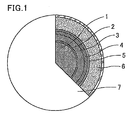
- Fig. 1 is a schematic view illustrating a preferred embodiment of the electroconductive microparticles of the present invention.
- the electroconductive microparticle shown in Fig. 1 includes, on the surface of a resin core particle 1, a base metal layer 2, an electroconductive metal layer 3, a barrier layer 4, a copper layer 5, and a solder layer 6 formed in said order. On the surface of the solder layer 6, at least one of nickel and cobalt 7 is adhered.
- the electroconductive microparticles of the present invention may be produced by any method, and a conventionally known method may be employed.
- the electroconductive microparticles of the present invention having a structure as illustrated in Fig. 1 can be produced by the following method.
- a nickel layer (hereafter, also referred to as a base nickel plating layer) as a base plating layer is formed on the surface of the core particle by electroless plating.
- an electroconductive metal layer is formed on the surface of the base nickel plating layer.
- the method for forming the electroconductive metal layer is not particularly limited, and examples thereof include electrolytic plating and electroless plating.
- a barrier layer such as a nickel layer is formed.
- the method for forming the nickel layer is not particularly limited, and examples thereof include electrolytic plating and electroless plating.
- a copper layer is formed on the surface of the barrier layer.
- the method for forming the copper layer is not particularly limited, and examples thereof include electrolytic plating and electroless plating.
- solder layer containing tin is formed on the surface of the copper layer.
- the method for forming the solder layer is not particularly limited, and examples thereof include electrolytic plating.
- At least one of nickel and cobalt is adhered.
- the method for adhering at least one of nickel and cobalt to the surface of the solder layer is not particularly limited, and examples thereof include sputtering and electroless plating.
- An anisotropic electroconductive material can be produced by dispersing the electroconductive microparticles of the present invention in a binder resin. Such an anisotropic electroconductive material is also encompassed by the present invention.
- anisotropic electroconductive material of the present invention examples include anisotropic electroconductive pastes, anisotropic electroconductive ink, anisotropic electroconductive adhesives, anisotropic electroconductive films, and anisotropic electroconductive sheets.
- the binder resin is not particularly limited, and examples thereof include vinyl resins, thermoplastic resins, curable resins, thermoplastic block copolymers, and elastomers.
- the vinyl resins are not particularly limited, and examples thereof include vinyl acetate resins, acrylic resins, and styrene resins.
- the thermoplastic resins are not particularly limited, and examples thereof include polyolefin resins, ethylene-vinyl acetate copolymers, and polyamide resins.
- the curable resins are not particularly limited, and examples thereof include epoxy resins, urethane resins, polyimide resins, and unsaturated polyester resins.
- thermoplastic block copolymers are not particularly limited, and examples thereof include styrene-butadiene-styrene block copolymers, styrene-isoprene-styrene block copolymers, hydrogenated styrene-butadiene-styrene block copolymers, and hydrogenated styrene-isoprene-styrene block copolymers. Each of these resins may be used alone or two or more of these may be used in combination.
- the curable resin may be any of a cold setting resin, a thermosetting resin, a photocurable resin, and a moisture curable resin.
- the anisotropic electroconductive material of the present invention may optionally contain various additives such as bulking agents, plasticizers, adhesiveness improvers, antioxidants, heat stabilizers, light stabilizers, ultraviolet absorbers, colorants, flame retardants, and organic solvents.
- additives such as bulking agents, plasticizers, adhesiveness improvers, antioxidants, heat stabilizers, light stabilizers, ultraviolet absorbers, colorants, flame retardants, and organic solvents.
- the method for producing the anisotropic electroconductive material of the present invention is not particularly limited.
- the electroconductive microparticles of the present invention are added to the binder resin and mixed to be dispersed uniformly, thereby producing an anisotropic electroconductive paste, anisotropic electroconductive ink, anisotropic electroconductive adhesive, or the like.
- the electroconductive microparticles of the present invention are added to the binder resin and dispersed uniformly or heat-molten.
- the resulting product is applied to a release-treated surface of a mold-release material (e.g., a mold-release paper, a mold-release film) to a predetermined thickness and optionally dried or cooled, thereby producing an anisotropic electroconductive film, anisotropic electroconductive sheet, or the like.
- a mold-release material e.g., a mold-release paper, a mold-release film
- the production method can be selected as appropriate corresponding to the kind of the anisotropic electroconductive material.
- the binder resin and the electroconductive microparticles of the present invention may be individually used as an anisotropic electroconductive material, without being mixed together.
- An electroconductive connection structure comprising the electroconductive microparticles of the present invention or the anisotropic electroconductive material of the present invention is also encompassed by the present invention.
- the electroconductive connection structure of the present invention is an electroconductive connection structure wherein the electroconductive microparticles of the present invention or the anisotropic electroconductive material of the present invention is filled between a pair of circuit substrates to connect the circuit substrates.
- the present invention can provide electroconductive microparticles which hardly cause disconnection due to breakage of connection interfaces between electrodes and the electroconductive microparticles even under application of an impact by dropping or the like and are less likely to be fatigued even after repetitive heating and cooling.
- the present invention can also provide an anisotropic electroconductive material and an electroconductive connection structure each produced using the electroconductive microparticles.
- Fig. 1 is a schematic view illustrating a preferred embodiment of the electroconductive microparticles of the present invention.
- Divinylbenzene (50 parts by weight) and tetramethylol methane tetraacrylate (50 parts by weight) were copolymerized to produce resin core particles (average particle size of 180 ⁇ m, CV value of 0.42%).
- Electroless nickel plating was performed on the resulting core particles to form a base nickel plating layer having a thickness of 0.3 ⁇ m on the surface of each core particle.
- a copper layer (electroconductive metal layer) having a thickness of 7 ⁇ m was formed thereon by electrolytic copper plating.
- a nickel layer (barrier layer) having a thickness of 0.6 ⁇ m was formed thereon by electrolytic nickel plating.
- a copper layer having a thickness of 1 ⁇ m was formed thereon by electrolytic copper plating.
- a solder layer containing tin with a thickness of 34 ⁇ m was formed thereon by electrolytic plating.
- the electrolytic plating liquid was filtered and the resulting particles were washed with water.
- electroconductive microparticles each including, on the surface of a core particle, a base metal layer, an electroconductive metal layer, a barrier layer, a copper layer, and a solder layer formed in said order.
- the ratio of copper contained in the copper layer directly in contact with the solder layer relative to tin contained in the solder layer was 2.6% by weight.
- Electroconductive microparticles each including a base metal layer, an electroconductive metal layer, a barrier layer, a copper layer, and a solder layer formed in said order on the surface of a core particle were produced in the same manner as in Example 1, except that the copper layer directly in contact with the solder layer had a thickness of 0.4 ⁇ m.
- the ratio of copper contained in the copper layer directly in contact with the solder layer relative to tin contained in the solder layer was 1.0% by weight.
- Electroconductive microparticles each including a base metal layer, an electroconductive metal layer, a barrier layer, a copper layer, and a solder layer formed in said order on the surface of a core particle were produced in the same manner as in Example 1, except that the copper layer directly in contact with the solder layer had a thickness of 2 ⁇ m.
- the ratio of copper contained in the copper layer directly in contact with the solder layer relative to tin contained in the solder layer was 5.0% by weight.
- Electroconductive microparticles each including a base metal layer, an electroconductive metal layer, a barrier layer, a copper layer, and a solder layer formed in said order on the surface of a core particle were produced in the same manner as in Example 1, except that the copper layer directly in contact with the solder layer had a thickness of 0.2 ⁇ m.
- the ratio of copper contained in the copper layer directly in contact with the solder layer relative to tin contained in the solder layer was 0.5% by weight.
- Electroconductive microparticles each including a base metal layer, an electroconductive metal layer, a barrier layer, a copper layer, a solder layer, and nickel adhered to the solder layer formed in said order on the surface of a core particle were produced in the same manner as in Example 1, except that nickel was adhered to the surface of the solder layer by sputtering.
- Electroconductive microparticles each including a base metal layer, an electroconductive metal layer, a barrier layer, a copper layer, a solder layer, and nickel adhered to the solder layer formed in said order on the surface of a core particle were produced in the same manner as in Example 1, except that nickel was adhered to the surface of the solder layer by electroless plating.
- Electroconductive microparticles each including a base metal layer, an electroconductive metal layer, a barrier layer, a copper layer, a solder layer, and cobalt adhered to the solder layer formed in said order on the surface of a core particle were produced in the same manner as in Example 1, except that cobalt was adhered to the surface of the solder layer by electroless plating.
- Divinylbenzene (50 parts by weight) and tetramethylol methane tetraacrylate (50 parts by weight) were copolymerized to give resin core particles (average particle size of 150 ⁇ m, CV value of 0.38%).
- Electroless nickel plating was performed on the resulting core particles to form a base nickel plating layer having a thickness of 0.3 ⁇ m on the surface of each particle.
- a copper layer (electroconductive metal layer) having a thickness of 10 ⁇ m was formed thereon by electrolytic copper plating.
- a nickel layer (barrier layer) having a thickness of 0.6 ⁇ m was formed thereon by electrolytic nickel plating.
- a copper layer having a thickness of 0.5 ⁇ m was formed thereon by electrolytic copper plating.
- a solder layer containing tin with a thickness of 40 ⁇ m was formed thereon by electrolytic plating.
- the electrolytic plating liquid was filtered and the resulting particles were washed with water.
- electroconductive microparticles each including, on the surface of a core particle, a base metal layer, an electroconductive metal layer, a barrier layer, a copper layer, and a solder layer formed in said order.
- the ratio of copper contained in the copper layer directly in contact with the solder layer relative to tin contained in the solder layer was 1.0% by weight.
- Electroconductive microparticles each including a base metal layer, an electroconductive metal layer, a barrier layer, a copper layer, a solder layer, and nickel adhered to the solder layer formed in said order on the surface of a core particle were produced in the same manner as in Example 8, except that nickel was adhered to the surface of the solder layer by electroless plating.
- Electroconductive microparticles each including a base metal layer, an electroconductive metal layer, a barrier layer, a copper layer, a solder layer, and cobalt adhered to the solder layer formed in said order on the surface of a core particle were produced in the same manner as in Example 1, except that cobalt was adhered to the surface of the solder layer by electroless plating.
- Electroconductive microparticles each including a base metal layer, an electroconductive metal layer, a barrier layer, and a solder layer formed in said order on the surface of a core particle were produced in the same manner as in Example 1, except that the copper layer directly in contact with the solder layer was not formed.
- Electroconductive microparticles each including a base metal layer, an electroconductive metal layer, a barrier layer, a copper layer, and a solder layer formed in said order on the surface of a core particle were produced in the same manner as in Example 1, except that the copper layer directly in contact with the solder layer was formed by electroless plating and had a thickness of 0.05 ⁇ m.
- the ratio of copper contained in the copper layer directly in contact with the solder layer relative to tin contained in the solder layer was 0.1% by weight.
- Electroconductive microparticles each including a base metal layer, an electroconductive metal layer, a barrier layer, a copper layer, and a solder layer formed in said order on the surface of a core particle were produced in the same manner as in Example 1, except that the copper layer directly in contact with the solder layer had a thickness of 4 ⁇ m.
- the ratio of copper contained in the copper layer directly in contact with the solder layer relative to tin contained in the solder layer was 10% by weight.
- Electroconductive microparticles each including a base metal layer, an electroconductive metal layer, a barrier layer, a copper layer, a solder layer, and nickel adhered to the solder layer formed in said order on the surface of a core particle were produced in the same manner as in Comparative Example 2, except that nickel was adhered to the surface of the solder layer by electroless plating.
- Electroconductive microparticles each including a base metal layer, an electroconductive metal layer, a barrier layer, a copper layer, a solder layer, and cobalt adhered to the solder layer formed in said order on the surface of a core particle were produced in the same manner as in Comparative Example 2, except that cobalt was adhered to the surface of the solder layer by electroless plating.
- Electroconductive microparticles each including a base metal layer, an electroconductive metal layer, a barrier layer, and a solder layer formed in said order on the surface of a core particle were produced in the same manner as in Example 8, except that the copper layer directly in contact with the solder layer was not formed.
- Electroconductive microparticles each including a base metal layer, an electroconductive metal layer, a barrier layer, a copper layer, and a solder layer formed in said order on the surface of a core particle were produced in the same manner as in Example 8, except that the copper layer directly in contact with the solder layer was formed by electroless plating and had a thickness of 0.1 ⁇ m.
- the ratio of copper contained in the copper layer directly in contact with the solder layer relative to tin contained in the solder layer was 0.2% by weight.
- Electroconductive microparticles each including a base metal layer, an electroconductive metal layer, a barrier layer, a copper layer, a solder layer, and nickel adhered to the solder layer formed in said order on the surface of a core particle were produced in the same manner as in Comparative Example 7, except that nickel was adhered to the surface of the solder layer by electroless plating.
- Electroconductive microparticles each including a base metal layer, an electroconductive metal layer, a barrier layer, a copper layer, a solder layer, and cobalt adhered to the solder layer formed in said order on the surface of a core particle were produced in the same manner as in Comparative Example 2, except that cobalt was adhered to the surface of the solder layer by electroless plating.
- Each of the obtained electroconductive microparticles was heated at 150°C for 12 hours, and the cross sections of the particles were taken. Five particles were selected and two points of each particle (10 points in total) were measured for the copper concentration (% by weight) of the solder layer with SEM-EDX. The minimum value, the maximum value, and the arithmetic average of the copper concentrations were determined.
- Silicon chips (5 mm in height ⁇ 5 mm in width) each provided with 121 electrode lands (diameter of 230 ⁇ m) at 0.4 mm pitch were prepared, and a flux ("WS-9160-M7" by Cookson Electronics) was applied to the electrode lands.
- a flux ("WS-9160-M7" by Cookson Electronics) was applied to the electrode lands.
- Each of the obtained electroconductive microparticles was placed on all the electrode lands and subjected to reflowing (heating temperature of 250°C, 30 seconds) to be mounted on the electrode lands.
- solder paste (“M705-GRN360-K2-V” by Senju Metal Industry Co., Ltd.) was applied to a printed substrate having a copper electrode (diameter of 250 ⁇ m) formed thereon. Fifteen silicon chips with the electroconductive microparticles mounted thereon were placed on the printed substrate and subjected to reflowing (heating temperature of 250°C, 30 seconds) to be mounted on the printed substrate. In this manner, an electroconductive connection structure was prepared.
- the drop strength test was performed on the obtained electroconductive connection structure in conformity with JESD22-B111 of the JEDEC standard. Since the obtained electroconductive connection structure had a daisy chain circuit formed therein, even a disconnection of the electrode land at only one point can be detected.
- the electrode lands were formed in the copper layer. The same shall apply in the following.
- a silicon chip (5 mm in height ⁇ 5 mm in width) provided with 121 electrode lands (diameter of 230 ⁇ m) at 0.4 mm pitch was prepared, and a flux ("WS-9160-M7" by Cookson Electronics) was applied to the electrode lands.
- a flux ("WS-9160-M7" by Cookson Electronics) was applied to the electrode lands.
- Each of the obtained electroconductive microparticles was placed on all the electrode lands and subjected to reflowing (heating temperature of 250°C, 30 seconds) to be mounted on the electrode lands.
- solder paste (“M705-GRN360-K2-V” by Senju Metal Industry Co., Ltd.) was applied to a printed substrate having a copper electrode (diameter of 250 ⁇ m) formed thereon.
- One silicon chip with the electroconductive microparticles mounted thereon was placed on the printed substrate and subjected to reflowing (heating temperature of 250°C, 30 seconds) to be mounted on the printed substrate. In this manner, an electroconductive connection structure was obtained.
- the temperature was kept at -40°C for 10 minutes, increased from -40°C to 125°C over 2 minutes, kept at 125°C for 10 minutes, and decreased from 125°C to -40°C over 2 minutes.
- the evaluation of the temperature cycle test was performed based on the following criteria. ⁇ (Good): 1000 cycles or more were repeated before the disconnection of the electroconductive connection structure was confirmed. ⁇ (Poor): Less than 1000 cycles were repeated before the disconnection of the electroconductive connection structure was confirmed.
- Example 1 The particles of Example 1 were dispersed in a binder resin and the circuit connection was executed. As a result, electrical connection was confirmed.
- the present invention can provide electroconductive microparticles which are less likely to cause disconnection due to breakage of connection interfaces between electrodes and the electroconductive microparticles even under application of an impact by dropping or the like and are less likely to be fatigued even after repetitive heating and cooling.
- the present invention can further provide an anisotropic electroconductive material and an electroconductive connection structure each produced using the electroconductive microparticles.
Landscapes
- Chemical & Material Sciences (AREA)
- Engineering & Computer Science (AREA)
- Mechanical Engineering (AREA)
- Organic Chemistry (AREA)
- Materials Engineering (AREA)
- Metallurgy (AREA)
- Chemical Kinetics & Catalysis (AREA)
- Microelectronics & Electronic Packaging (AREA)
- General Chemical & Material Sciences (AREA)
- Electrochemistry (AREA)
- Power Engineering (AREA)
- Computer Hardware Design (AREA)
- Manufacturing & Machinery (AREA)
- Crystallography & Structural Chemistry (AREA)
- Spectroscopy & Molecular Physics (AREA)
- Dispersion Chemistry (AREA)
- Physics & Mathematics (AREA)
- Conductive Materials (AREA)
- Electric Connection Of Electric Components To Printed Circuits (AREA)
- Non-Insulated Conductors (AREA)
- Laminated Bodies (AREA)
- Manufacture Of Metal Powder And Suspensions Thereof (AREA)
- Powder Metallurgy (AREA)
Abstract
Description
- The present invention relates to electroconductive microparticles which are less likely to cause disconnection due to breakage of connection interfaces between electrodes and the electroconductive microparticles even under application of an impact by dropping or the like and are less likely to be fatigued even after repetitive heating and cooling. The present invention also relates to an anisotropic electroconductive material and an electroconductive connection structure each produced using the electroconductive microparticles.
- ICs or LSIs, in a conventional way of producing an electronic circuit substrate, have been bonded onto a printed substrate through soldering of the electrodes thereof to the printed substrate. Soldering, however, does not enable effective bonding of the ICs or LSIs onto the printed substrate, and does not contribute to an increase in the packaging density of ICs or LSIs.
- To solve the above problem, the ball grid array (BGA) technique has been developed which uses solder in a ball shape, so-called "solder balls", to bond ICs or LSIs onto the substrate. In the case of using the BGA technique, solder balls mounted on a chip or a substrate are molten at high temperatures, thereby bonding the substrate to the chip. As a result, the production efficiency of electronic circuit substrates is improved. Moreover, electronic circuit substrates with improved packaging density of chips can be produced.
- However, multi-layer substrates have been more used in recent years, and those multi-layer substrates, sensitive to the environmental conditions, are sometimes distorted, expanded or contracted to cause disconnection of the connection portions between substrates.
- For example, when a solder ball is used to connect a semiconductor to a substrate, the solder ball undergoes stress because the semiconductor and the substrate are different in the linear expansion coefficient. As a result, the solder ball may have a crack to cause disconnection.
- To solve such a problem, Patent Literature 1 discloses electroconductive microparticles each including a resin fine particle, an electroconductive metal layer containing a highly conductive metal on the surface of the resin fine particle, and a solder layer formed on the surface of the electroconductive metal layer. Such electroconductive microparticles can ease the stress applied thereto with soft resin fine particles. Since a solder layer is formed on the outermost surface of each electroconductive microparticle, electrodes are easily conductively connected to each other.
- When electroconductive microparticles each with a solder layer formed thereon are mounted on electrodes of substrates, the electroconductive microparticles are placed on an electrode formed on one substrate. The solder layer is molten by reflowing, so that the electroconductive microparticles are immobilized on the electrode. Then, the substrates are arranged in such a manner that an electrode formed on the other substrate faces the electrode formed on the one substrate, and reflowing is performed to conductively connect the electrodes of the substrates.
- If electroconductive microparticles each including a core particle and a solder layer formed on the surface of the core particle as disclosed in Patent Literature 1 are used for conductive connection of electronic circuit substrates having currently dominant copper electrodes, however, disconnection is likely to occur due to breakage of connection interfaces under application of an impact by dropping or the like. During the use of an electronic device, electronic components generate heat to increase the temperature inside the electronic device. After the use, the temperature inside the electronic device is lowered to ambient temperature. In this manner, the electronic device is subjected to repetitive heating and cooling, i.e., a "heat cycle". Repetitive heat cycles also may cause breakage of connection interfaces between electrodes and electroconductive microparticles, resulting in disconnection.
- Patent Literature 1:
JP-A 2001-220691 - The present invention aims to provide electroconductive microparticles which are less likely to cause disconnection due to breakage of connection interfaces between electrodes and the electroconductive microparticles even under application of an impact by dropping or the like and are less likely to be fatigued even after repetitive heating and cooling. The present invention aims to provide an anisotropic electroconductive material and an electroconductive connection structure each produced using the electroconductive microparticles.
- The present invention relates to electroconductive microparticles each including at least an electroconductive metal layer, a barrier layer, a copper layer, and a solder layer containing tin that are laminated in said order on a surface of a core particle made of a resin or metal, the copper layer and the solder layer being in contact with each other directly, the copper layer directly in contact with the solder layer containing copper at a ratio of 0.5 to 5 % by weight relative to tin contained in the solder layer.
- The present invention is specifically described in the following.
- The present inventors intensively studied about the cause of the disconnection due to breakage of connection interfaces under application of an impact by dropping or the like or after repetitive heat cycles when electroconductive microparticles each including a core particle and a solder layer formed on the surface of the core particle are used for conductive connection of electronic circuit substrates having copper electrodes. As a result, they found out that the cause is formation of a tin/copper intermetallic compound (hereafter, also simply referred to as an "intermetallic compound") on the connection interfaces. In other words, tin contained in the solder layer presumably incorporates a part of copper included in the electrodes when the solder layer is molten by heating upon reflowing. As a result, pure copper in the electrodes is reduced, and a large amount of an intermetallic compound is formed on the connection interfaces (hereafter, such a phenomenon is also referred to as "copper erosion"). Since the intermetallic compound is harder and more brittle than copper or solder, portions made of the intermetallic compound formed on the connection interfaces are presumably broken upon application of an impact by dropping or the like or after repetitive heat cycles, to cause disconnection.
- The present inventors made further intensive studies to find out that, in the case where a solder layer is made in contact with a copper layer for the purpose of setting the ratio of copper to tin contained in the solder layer within a predetermined range, such electroconductive microparticles are less likely to cause disconnection due to breakage of connection interfaces even under application of an impact by dropping or the like or after repetitive heat cycles, thereby completing the present invention.
- Directly contacting the solder layer of each electroconductive microparticle with the copper layer in advance allows copper from the copper layer to be preferentially diffused into the solder layer and dissolved therein when the solder layer is molten by heating upon reflowing. In such a case, "copper erosion" for further incorporating copper is suppressed to keep pure copper in the electrodes, and formation of a large amount of an intermetallic compound is avoided.
- The electroconductive microparticles of the present invention each have a structure including at least an electroconductive metal layer, a barrier layer, a copper layer, and a solder layer containing tin that are laminated in said order on the surface of a core particle made of a resin or metal.
- Examples of the resin forming the core particle include: polyolefin resins such as polyethylene resin, polypropylene resin, polystyrene resin, polyisobutylene resin, polybutadiene resin, polyvinyl chloride resin, polyvinylidene chloride resin, and polytetrafluoroethylene resin; acrylic resins such as polymethyl methacrylate resin, and polymethyl acrylate resin; and polyalkylene terephthalate resin, polysulfone resin, polycarbonate resin, polyamide resin, phenol formaldehyde resin, melamine formaldehyde resin, benzoguanamine formaldehyde resin, and urea-formaldehyde resin.
- Examples of the metal forming the core particle include copper, nickel, and silver.
- In particular, in the case of using resin core particles, even if a substrate conductively connected with the electroconductive microparticles of the present invention is distorted, expanded, or contracted due to a change in the environment, the electroconductive microparticles can ease the stress applied thereto with soft resin. In the case of using metal core particles, even if a chip generates heat, the particles are expected to transfer the heat to the substrate, thereby improving heat radiation.
- In the case of resin core particles, the preferable lower limit of the 10% K value of the core particles is 1000 MPa and the preferable upper limit thereof is 15000 MPa, and the more preferable lower limit is 2000 MPa and the more preferable upper limit is 10000 MPa, in terms of the shape of electroconductive microparticles when the microparticles are compression-deformed and damage to the electrode.
- The 10% K value can be determined by measuring, with a microcompression tester (e.g., "PCT-200" produced by Shimadzu Corporation), the compression displacement (mm) of the resin core particles when the particles are compressed by a flat end face of a diamond column indenter (diameter of 50 µm) under the conditions of a compression speed of 2.6 mN/second and a maximum test load of 10 g; and substituting the values into the following equation.

F: Force (N) in 10% compressive deformation of resin core particles
S: Compression displacement (mm) in 10% compressive deformation of resin core particles
R: Radius (mm) of resin core particles - The preferable lower limit of the average particle size of the core particles is 10 µm and the preferable upper limit thereof is 2000 µm, in terms of the dispersibility of the core particles and electroconductive microparticles and the usability as an anisotropic electroconductive material. The more preferable lower limit of the average particle size is 30 µm and the more preferable upper limit thereof is 1500 µm. The still more preferable lower limit of the average particle size is 50 µm and the still more preferable upper limit thereof is 1000 µm.
- The average particle size of the core particles means the average of diameters obtained by measuring 50 core particles selected at random with an optical microscope or electron microscope.
- The preferable upper limit of the CV value of the particle size of the core particles is 15% in terms of the connection reliability of the electroconductive microparticles. The more preferable upper limit of CV value is 10%. The CV value is a numerical value in percentage (%) obtained by dividing the standard deviation by the average particle size.
- The resin core particles may be produced by any method, and examples of the method include a polymerization method, a method using a polymer protectant, and a method using a surfactant.
- The polymerization method is not particularly limited, and examples thereof include emulsion polymerization, suspension polymerization, seed polymerization, dispersion polymerization, and dispersion seed polymerization.
- The electroconductive metal layer has a function of enhancing the electrical connection reliability between the electroconductive microparticles and the electrodes.
- The electroconductive metal layer may be formed directly on each core particle. Alternatively, a base metal layer such as a nickel layer may be formed between the electroconductive metal layer and the core particle.
- Examples of the metal forming the electroconductive metal layer include gold, silver, copper, platinum, palladium, cobalt, and nickel. In particular, the electroconductive metal layer preferably contains copper because copper exerts an excellent effect of enhancing the electrical connection reliability between the electroconductive microparticles and the electrodes.
- The thickness of the electroconductive metal layer is not particularly limited. In terms of the electroconductivity and the flexibility of the electroconductive microparticles, the preferable lower limit of the thickness is 1 µm and the preferable upper limit thereof is 70 µm. The more preferable lower limit of the thickness of the electroconductive metal layer is 3 µm and the more preferable upper limit thereof is 50 µm.
- The thickness of the electroconductive metal layer is determined by measuring the cross sections of 10 electroconductive microparticles selected at random with a scanning electron microscope (SEM), and arithmetically averaging the measured values.
- The barrier layer is positioned between the electroconductive metal layer and the copper layer and has a function of preventing diffusion of a metal contained in the electroconductive metal layer into the solder layer upon reflowing. Especially when the electroconductive metal layer contains copper, pure copper is reduced due to copper erosion upon reflowing, and a large amount of an intermetallic compound is formed. As a result, the electroconductive metal layer is embrittled to cause disconnection. Moreover, reduction of pure copper may possibly impair the electrical characteristics (electroconductivity).
- Exemplary materials of the barrier layer include nickel, titanium, tantalum, titanium nitride, zirconia, and zirconia nitride. In particular, the barrier layer preferably contains nickel because formation of the barrier layer becomes easy. The barrier layer preferably has an amorphous structure. Specific examples of the amorphous barrier layer include a nickel-phosphor layer and a nickel-boron layer. When the barrier layer has an amorphous structure, copper is less likely to be diffused into the solder layer because the grain boundary is reduced.
- The thickness of the barrier layer is not particularly limited. From the standpoint of preventing diffusion of a metal such as copper into the solder layer or formation of a hard and brittle intermetallic compound on the interface between the solder layer and the electroconductive metal layer, the preferable lower limit of the thickness is 0.2 µm and the preferable upper limit thereof is 5 µm. The more preferable lower limit of the thickness of the barrier layer is 0.5 µm and the more preferable upper limit thereof is 3 µm.
- The thickness of the barrier layer is determined by measuring the cross sections of 10 electroconductive microparticles selected at random with a scanning electron microscope (SEM); and arithmetically averaging the measured values.
- The electroconductive microparticles of the present invention each include a copper layer and a solder layer formed to be directly in contact with each other on the outer side of the barrier layer.
- The solder layer has a function of electroconductively connecting the electrodes of the substrates by being molten by heating upon reflowing. The solder layer is preferably formed on the outermost surface of the electroconductive microparticles.
- The solder layer contains tin.
- The solder layer preferably further contains silver. The solder layer containing silver can have a comparatively low melting point and high strength.
- The silver content of the solder layer is not particularly limited. The preferable lower limit of the ratio of silver to tin is 0.5% by weight and the preferable upper limit thereof is 10% by weight. When the silver content is within this range, a comparatively low melting point and high strength are both achieved.
- The solder layer may contain, in addition to tin and silver, metals such as antimony, bismuth, indium, germanium, aluminum, zinc, nickel, and cobalt. The solder layer may contain copper at a predetermined percentage as described later.
- The thickness of the solder layer is not particularly limited. In terms of the bondability to the electrodes and dispersibility of the electroconductive microparticles upon formation of the solder layer, the preferable lower limit of the thickness is 1 µm and the preferable upper limit thereof is 50 µm. The more preferable lower limit of the thickness of the solder layer is 3 µm and the more preferable upper limit thereof is 40 µm.
- The thickness of the solder layer is determined by measuring the cross sections of 10 electroconductive microparticles selected at random with a scanning electron microscope (SEM); and arithmetically averaging the measured values.
- The copper layer is formed in such a manner as to be directly in contact with the solder layer. The copper layer directly in contact with the solder layer allows copper in the copper layer to be preferentially diffused into the solder layer upon heat-melting to set the copper concentration of the solder layer within a predetermined range. In such a case, "copper erosion" is suppressed so that pure copper in the electrodes are kept. As a result, formation of a large amount of an intermetallic compound on the connection interfaces can be prevented.
- The lower limit of the ratio of copper contained in the copper layer directly in contact with the solder layer relative to tin contained in the solder layer is 0.5% by weight and the upper limit thereof is 5% by weight. If the ratio of copper is less than 0.5% by weight, diffusion of the copper into the solder layer upon reflowing fails to increase the copper concentration sufficiently, and "copper erosion" cannot be sufficiently suppressed. In such a case, pure copper in the electrodes cannot be kept, leading to a failure in prevention of formation of an intermetallic compound on the connection interfaces. If the ratio of copper is more than 5% by weight, the concentration of copper diffused into the solder layer upon reflowing is too high. In such a case, the melting point of solder increases to have an influence on mountability. The preferable upper limit of the ratio of copper contained in the copper layer directly in contact with the solder layer relative to tin contained in the solder layer is 3% by weight.
- For sufficient suppression of "copper erosion" and prevention of an increase in the melting point of solder, it is important to set the concentration of copper diffused into the solder layer when heat-melting the solder layer upon reflowing, within a predetermined range. In other words, the preferable lower limit of the concentration of the copper, at any given point of the solder layer, after heating at 150°C for 12 hours is 0.5% by weight and the preferable upper limit thereof is 40% by weight, and the more preferable lower limit is 0.7% by weight and the more preferable upper limit is 30% by weight. The ratio of copper contained in the copper layer directly in contact with the solder layer is determined to set the concentration of copper diffused into the solder layer when heat-melting the solder layer upon reflowing, within the above mentioned range.
- In the electroconductive microparticles of the present invention, at least one of nickel and cobalt may be further adhered to the surface of the solder layer. At least one of nickel and cobalt adhered to the surface of the solder layer micronizes the crystal structure of an intermetallic compound formed on the connection interfaces between the electroconductive microparticles and the electrodes after reflowing. Such electroconductive microparticles are further less likely to cause disconnection due to breakage of the connection interfaces even under application of an impact by dropping or the like or repetitive heat cycles.
- The adhesion herein refers to a state where a metal (at least one of nickel and cobalt) is present on the surface of the solder layer but a metal layer of at least one of nickel and cobalt completely covering the surface of the solder layer is not formed.
-
Fig. 1 is a schematic view illustrating a preferred embodiment of the electroconductive microparticles of the present invention. - The electroconductive microparticle shown in
Fig. 1 includes, on the surface of a resin core particle 1, abase metal layer 2, anelectroconductive metal layer 3, abarrier layer 4, acopper layer 5, and asolder layer 6 formed in said order. On the surface of thesolder layer 6, at least one of nickel andcobalt 7 is adhered. - The electroconductive microparticles of the present invention may be produced by any method, and a conventionally known method may be employed. For example, the electroconductive microparticles of the present invention having a structure as illustrated in
Fig. 1 can be produced by the following method. - When an electroconductive metal layer is formed on the surface of a resin core particle, a nickel layer (hereafter, also referred to as a base nickel plating layer) as a base plating layer is formed on the surface of the core particle by electroless plating.
- Next, an electroconductive metal layer is formed on the surface of the base nickel plating layer.
- The method for forming the electroconductive metal layer is not particularly limited, and examples thereof include electrolytic plating and electroless plating.
- On the surface of the electroconductive metal layer, a barrier layer such as a nickel layer is formed.
- The method for forming the nickel layer is not particularly limited, and examples thereof include electrolytic plating and electroless plating.
- On the surface of the barrier layer, a copper layer is formed.
- The method for forming the copper layer is not particularly limited, and examples thereof include electrolytic plating and electroless plating.
- Then, a solder layer containing tin is formed on the surface of the copper layer.
- The method for forming the solder layer is not particularly limited, and examples thereof include electrolytic plating.
- To the surface of the solder layer, at least one of nickel and cobalt is adhered.
- The method for adhering at least one of nickel and cobalt to the surface of the solder layer is not particularly limited, and examples thereof include sputtering and electroless plating.
- An anisotropic electroconductive material can be produced by dispersing the electroconductive microparticles of the present invention in a binder resin. Such an anisotropic electroconductive material is also encompassed by the present invention.
- Examples of the anisotropic electroconductive material of the present invention include anisotropic electroconductive pastes, anisotropic electroconductive ink, anisotropic electroconductive adhesives, anisotropic electroconductive films, and anisotropic electroconductive sheets.
- The binder resin is not particularly limited, and examples thereof include vinyl resins, thermoplastic resins, curable resins, thermoplastic block copolymers, and elastomers.
- The vinyl resins are not particularly limited, and examples thereof include vinyl acetate resins, acrylic resins, and styrene resins. The thermoplastic resins are not particularly limited, and examples thereof include polyolefin resins, ethylene-vinyl acetate copolymers, and polyamide resins. The curable resins are not particularly limited, and examples thereof include epoxy resins, urethane resins, polyimide resins, and unsaturated polyester resins. The thermoplastic block copolymers are not particularly limited, and examples thereof include styrene-butadiene-styrene block copolymers, styrene-isoprene-styrene block copolymers, hydrogenated styrene-butadiene-styrene block copolymers, and hydrogenated styrene-isoprene-styrene block copolymers. Each of these resins may be used alone or two or more of these may be used in combination.
- The curable resin may be any of a cold setting resin, a thermosetting resin, a photocurable resin, and a moisture curable resin.
- The anisotropic electroconductive material of the present invention may optionally contain various additives such as bulking agents, plasticizers, adhesiveness improvers, antioxidants, heat stabilizers, light stabilizers, ultraviolet absorbers, colorants, flame retardants, and organic solvents.
- The method for producing the anisotropic electroconductive material of the present invention is not particularly limited. In an exemplary method, the electroconductive microparticles of the present invention are added to the binder resin and mixed to be dispersed uniformly, thereby producing an anisotropic electroconductive paste, anisotropic electroconductive ink, anisotropic electroconductive adhesive, or the like. In another exemplary method for producing the anisotropic electroconductive material of the present invention, the electroconductive microparticles of the present invention are added to the binder resin and dispersed uniformly or heat-molten. The resulting product is applied to a release-treated surface of a mold-release material (e.g., a mold-release paper, a mold-release film) to a predetermined thickness and optionally dried or cooled, thereby producing an anisotropic electroconductive film, anisotropic electroconductive sheet, or the like. The production method can be selected as appropriate corresponding to the kind of the anisotropic electroconductive material.
- The binder resin and the electroconductive microparticles of the present invention may be individually used as an anisotropic electroconductive material, without being mixed together.
- An electroconductive connection structure comprising the electroconductive microparticles of the present invention or the anisotropic electroconductive material of the present invention is also encompassed by the present invention.
- The electroconductive connection structure of the present invention is an electroconductive connection structure wherein the electroconductive microparticles of the present invention or the anisotropic electroconductive material of the present invention is filled between a pair of circuit substrates to connect the circuit substrates.
- The present invention can provide electroconductive microparticles which hardly cause disconnection due to breakage of connection interfaces between electrodes and the electroconductive microparticles even under application of an impact by dropping or the like and are less likely to be fatigued even after repetitive heating and cooling. The present invention can also provide an anisotropic electroconductive material and an electroconductive connection structure each produced using the electroconductive microparticles.
-
Fig. 1 is a schematic view illustrating a preferred embodiment of the electroconductive microparticles of the present invention. - Embodiments of the present invention are specifically described with reference to, but not limited to, examples in the following.
- Divinylbenzene (50 parts by weight) and tetramethylol methane tetraacrylate (50 parts by weight) were copolymerized to produce resin core particles (average particle size of 180 µm, CV value of 0.42%).
- Electroless nickel plating was performed on the resulting core particles to form a base nickel plating layer having a thickness of 0.3 µm on the surface of each core particle. Next, a copper layer (electroconductive metal layer) having a thickness of 7 µm was formed thereon by electrolytic copper plating. A nickel layer (barrier layer) having a thickness of 0.6 µm was formed thereon by electrolytic nickel plating. A copper layer having a thickness of 1 µm was formed thereon by electrolytic copper plating. A solder layer containing tin with a thickness of 34 µm was formed thereon by electrolytic plating. Finally, the electrolytic plating liquid was filtered and the resulting particles were washed with water. The particles were then dried in a vacuum dryer at 50°C to give electroconductive microparticles each including, on the surface of a core particle, a base metal layer, an electroconductive metal layer, a barrier layer, a copper layer, and a solder layer formed in said order.
- In the obtained electroconductive microparticles, the ratio of copper contained in the copper layer directly in contact with the solder layer relative to tin contained in the solder layer was 2.6% by weight.
- Electroconductive microparticles each including a base metal layer, an electroconductive metal layer, a barrier layer, a copper layer, and a solder layer formed in said order on the surface of a core particle were produced in the same manner as in Example 1, except that the copper layer directly in contact with the solder layer had a thickness of 0.4 µm.
- In the obtained electroconductive microparticles, the ratio of copper contained in the copper layer directly in contact with the solder layer relative to tin contained in the solder layer was 1.0% by weight.
- Electroconductive microparticles each including a base metal layer, an electroconductive metal layer, a barrier layer, a copper layer, and a solder layer formed in said order on the surface of a core particle were produced in the same manner as in Example 1, except that the copper layer directly in contact with the solder layer had a thickness of 2 µm.
- In the obtained electroconductive microparticles, the ratio of copper contained in the copper layer directly in contact with the solder layer relative to tin contained in the solder layer was 5.0% by weight.
- Electroconductive microparticles each including a base metal layer, an electroconductive metal layer, a barrier layer, a copper layer, and a solder layer formed in said order on the surface of a core particle were produced in the same manner as in Example 1, except that the copper layer directly in contact with the solder layer had a thickness of 0.2 µm.
- In the obtained electroconductive microparticles, the ratio of copper contained in the copper layer directly in contact with the solder layer relative to tin contained in the solder layer was 0.5% by weight.
- Electroconductive microparticles each including a base metal layer, an electroconductive metal layer, a barrier layer, a copper layer, a solder layer, and nickel adhered to the solder layer formed in said order on the surface of a core particle were produced in the same manner as in Example 1, except that nickel was adhered to the surface of the solder layer by sputtering.
- Electroconductive microparticles each including a base metal layer, an electroconductive metal layer, a barrier layer, a copper layer, a solder layer, and nickel adhered to the solder layer formed in said order on the surface of a core particle were produced in the same manner as in Example 1, except that nickel was adhered to the surface of the solder layer by electroless plating.
- Electroconductive microparticles each including a base metal layer, an electroconductive metal layer, a barrier layer, a copper layer, a solder layer, and cobalt adhered to the solder layer formed in said order on the surface of a core particle were produced in the same manner as in Example 1, except that cobalt was adhered to the surface of the solder layer by electroless plating.
- Divinylbenzene (50 parts by weight) and tetramethylol methane tetraacrylate (50 parts by weight) were copolymerized to give resin core particles (average particle size of 150 µm, CV value of 0.38%).
- Electroless nickel plating was performed on the resulting core particles to form a base nickel plating layer having a thickness of 0.3 µm on the surface of each particle. Next, a copper layer (electroconductive metal layer) having a thickness of 10 µm was formed thereon by electrolytic copper plating. A nickel layer (barrier layer) having a thickness of 0.6 µm was formed thereon by electrolytic nickel plating. A copper layer having a thickness of 0.5 µm was formed thereon by electrolytic copper plating. A solder layer containing tin with a thickness of 40 µm was formed thereon by electrolytic plating. Finally, the electrolytic plating liquid was filtered and the resulting particles were washed with water. The particles were then dried in a vacuum dryer at 50°C to give electroconductive microparticles each including, on the surface of a core particle, a base metal layer, an electroconductive metal layer, a barrier layer, a copper layer, and a solder layer formed in said order.
- In the obtained electroconductive microparticles, the ratio of copper contained in the copper layer directly in contact with the solder layer relative to tin contained in the solder layer was 1.0% by weight.
- Electroconductive microparticles each including a base metal layer, an electroconductive metal layer, a barrier layer, a copper layer, a solder layer, and nickel adhered to the solder layer formed in said order on the surface of a core particle were produced in the same manner as in Example 8, except that nickel was adhered to the surface of the solder layer by electroless plating.
- Electroconductive microparticles each including a base metal layer, an electroconductive metal layer, a barrier layer, a copper layer, a solder layer, and cobalt adhered to the solder layer formed in said order on the surface of a core particle were produced in the same manner as in Example 1, except that cobalt was adhered to the surface of the solder layer by electroless plating.
- Electroconductive microparticles each including a base metal layer, an electroconductive metal layer, a barrier layer, and a solder layer formed in said order on the surface of a core particle were produced in the same manner as in Example 1, except that the copper layer directly in contact with the solder layer was not formed.
- Electroconductive microparticles each including a base metal layer, an electroconductive metal layer, a barrier layer, a copper layer, and a solder layer formed in said order on the surface of a core particle were produced in the same manner as in Example 1, except that the copper layer directly in contact with the solder layer was formed by electroless plating and had a thickness of 0.05 µm.
- In the obtained electroconductive microparticles, the ratio of copper contained in the copper layer directly in contact with the solder layer relative to tin contained in the solder layer was 0.1% by weight.
- Electroconductive microparticles each including a base metal layer, an electroconductive metal layer, a barrier layer, a copper layer, and a solder layer formed in said order on the surface of a core particle were produced in the same manner as in Example 1, except that the copper layer directly in contact with the solder layer had a thickness of 4 µm.
- In the obtained electroconductive microparticles, the ratio of copper contained in the copper layer directly in contact with the solder layer relative to tin contained in the solder layer was 10% by weight.
- Electroconductive microparticles each including a base metal layer, an electroconductive metal layer, a barrier layer, a copper layer, a solder layer, and nickel adhered to the solder layer formed in said order on the surface of a core particle were produced in the same manner as in Comparative Example 2, except that nickel was adhered to the surface of the solder layer by electroless plating.
- Electroconductive microparticles each including a base metal layer, an electroconductive metal layer, a barrier layer, a copper layer, a solder layer, and cobalt adhered to the solder layer formed in said order on the surface of a core particle were produced in the same manner as in Comparative Example 2, except that cobalt was adhered to the surface of the solder layer by electroless plating.
- Electroconductive microparticles each including a base metal layer, an electroconductive metal layer, a barrier layer, and a solder layer formed in said order on the surface of a core particle were produced in the same manner as in Example 8, except that the copper layer directly in contact with the solder layer was not formed.
- Electroconductive microparticles each including a base metal layer, an electroconductive metal layer, a barrier layer, a copper layer, and a solder layer formed in said order on the surface of a core particle were produced in the same manner as in Example 8, except that the copper layer directly in contact with the solder layer was formed by electroless plating and had a thickness of 0.1 µm.
- In the obtained electroconductive microparticles, the ratio of copper contained in the copper layer directly in contact with the solder layer relative to tin contained in the solder layer was 0.2% by weight.
- Electroconductive microparticles each including a base metal layer, an electroconductive metal layer, a barrier layer, a copper layer, a solder layer, and nickel adhered to the solder layer formed in said order on the surface of a core particle were produced in the same manner as in Comparative Example 7, except that nickel was adhered to the surface of the solder layer by electroless plating.
- Electroconductive microparticles each including a base metal layer, an electroconductive metal layer, a barrier layer, a copper layer, a solder layer, and cobalt adhered to the solder layer formed in said order on the surface of a core particle were produced in the same manner as in Comparative Example 2, except that cobalt was adhered to the surface of the solder layer by electroless plating.
- The electroconductive microparticles of the examples and the comparative examples were evaluated for the following items. Table 1 shows the results.
- Each of the obtained electroconductive microparticles was heated at 150°C for 12 hours, and the cross sections of the particles were taken. Five particles were selected and two points of each particle (10 points in total) were measured for the copper concentration (% by weight) of the solder layer with SEM-EDX. The minimum value, the maximum value, and the arithmetic average of the copper concentrations were determined.
- Silicon chips (5 mm in height × 5 mm in width) each provided with 121 electrode lands (diameter of 230 µm) at 0.4 mm pitch were prepared, and a flux ("WS-9160-M7" by Cookson Electronics) was applied to the electrode lands. Each of the obtained electroconductive microparticles was placed on all the electrode lands and subjected to reflowing (heating temperature of 250°C, 30 seconds) to be mounted on the electrode lands.
- Next, a solder paste ("M705-GRN360-K2-V" by Senju Metal Industry Co., Ltd.) was applied to a printed substrate having a copper electrode (diameter of 250 µm) formed thereon. Fifteen silicon chips with the electroconductive microparticles mounted thereon were placed on the printed substrate and subjected to reflowing (heating temperature of 250°C, 30 seconds) to be mounted on the printed substrate. In this manner, an electroconductive connection structure was prepared.
- The drop strength test was performed on the obtained electroconductive connection structure in conformity with JESD22-B111 of the JEDEC standard. Since the obtained electroconductive connection structure had a daisy chain circuit formed therein, even a disconnection of the electrode land at only one point can be detected.
- The number of times of dropping needed for disconnecting all the 15 silicon chips was counted.
- Here, the electrode lands were formed in the copper layer. The same shall apply in the following.
- A silicon chip (5 mm in height ×5 mm in width) provided with 121 electrode lands (diameter of 230 µm) at 0.4 mm pitch was prepared, and a flux ("WS-9160-M7" by Cookson Electronics) was applied to the electrode lands. Each of the obtained electroconductive microparticles was placed on all the electrode lands and subjected to reflowing (heating temperature of 250°C, 30 seconds) to be mounted on the electrode lands.
- Next, a solder paste ("M705-GRN360-K2-V" by Senju Metal Industry Co., Ltd.) was applied to a printed substrate having a copper electrode (diameter of 250 µm) formed thereon. One silicon chip with the electroconductive microparticles mounted thereon was placed on the printed substrate and subjected to reflowing (heating temperature of 250°C, 30 seconds) to be mounted on the printed substrate. In this manner, an electroconductive connection structure was obtained.
- Since the resulting electroconductive connection structure had a daisy chain circuit formed therein, even a disconnection of the electrode land at only one point can be detected.
- A temperature cycle test in which a temperature change from -40°C to 125°C was set as one cycle was performed on the resulting electroconductive connection structure. In the heat profile of the temperature cycle test, the temperature was kept at -40°C for 10 minutes, increased from -40°C to 125°C over 2 minutes, kept at 125°C for 10 minutes, and decreased from 125°C to -40°C over 2 minutes.
- The evaluation of the temperature cycle test was performed based on the following criteria.
○ (Good): 1000 cycles or more were repeated before the disconnection of the electroconductive connection structure was confirmed.
× (Poor): Less than 1000 cycles were repeated before the disconnection of the electroconductive connection structure was confirmed.[Table 1] Ratio of copper directly in contact with solder layer (% by weight) Copper concentration of solder layer after heating at 150°C for 12 hours (% by weight) Number of times of dropping in drop strength test (times) Temperature cycle test Minimum Maximum Average Example 1 2.6 0.76 30.54 11.24 1289 ○ Example 2 1.0 0.63 15.35 6.83 1157 ○ Example 3 5.0 1.96 38.24 13.99 1092 ○ Example 4 0.5 0.51 4.34 2.20 1016 ○ Example 5 2.6 0.89 28.15 10.75 1493 ○ Example 6 2.6 1.02 29.57 9.94 1528 ○ Example 7 2.6 0.63 23.40 11.41 1669 ○ Example 8 1.0 0.59 18.16 7.22 1017 ○ Example 9 1.0 0.92 20.15 7.87 1249 ○ Example 10 1.0 1.06 15.10 7.75 1364 ○ Comparative Example 1 0.0 0.02 0.15 0.09 589 × Comparative Example 2 0.1 0.08 0.43 0.23 673 × Comparative Example 3 10.0 8.96 62.58 40.26 439 × Comparative Example 4 0.1 0.05 0.41 0.23 804 × Comparative Example 5 0.1 0.06 0.49 0.27 859 × Comparative Example 6 0.0 0.01 0.14 0.06 496 × Comparative Example 7 0.2 0.08 0.64 0.34 587 × Comparative Example 8 0.2 0.16 0.87 0.42 665 × Comparative Example 9 0.1 0.08 0.62 0.39 718 × - The particles of Example 1 were dispersed in a binder resin and the circuit connection was executed. As a result, electrical connection was confirmed.
- The present invention can provide electroconductive microparticles which are less likely to cause disconnection due to breakage of connection interfaces between electrodes and the electroconductive microparticles even under application of an impact by dropping or the like and are less likely to be fatigued even after repetitive heating and cooling. The present invention can further provide an anisotropic electroconductive material and an electroconductive connection structure each produced using the electroconductive microparticles.
-
- 1. Core particle
- 2. Base metal layer
- 3. Electroconductive metal layer
- 4. Barrier layer
- 5. Copper layer
- 6. Solder layer
- 7. At least one of nickel and cobalt adhered to solder layer
Claims (5)
- Electroconductive microparticles each comprising at least an electroconductive metal layer, a barrier layer, a copper layer, and a solder layer containing tin that are laminated in said order on a surface of a core particle made of a resin or metal,
the copper layer and the solder layer being in contact with each other directly, the copper layer directly in contact with the solder layer containing copper at a ratio of 0.5 to 5% by weight relative to tin contained in the solder layer. - The electroconductive microparticles according to claim 1,
wherein the concentration of the copper at any given point in the solder layer is 0.5 to 40% by weight after heating at 150°C for 12 hours. - The electroconductive microparticles according to claim 1 or 2,
wherein at least one of nickel and cobalt is adhered to the surface of the solder layer. - An anisotropic electroconductive material comprising the electroconductive microparticles according to claim 1, 2, or 3 dispersed in a binder resin.
- An electroconductive connection structure comprising the electroconductive microparticles according to claim 1, 2, or 3 or the anisotropic electroconductive material according to claim 4.
Applications Claiming Priority (2)
| Application Number | Priority Date | Filing Date | Title |
|---|---|---|---|
| JP2013039800 | 2013-02-28 | ||
| PCT/JP2014/055035 WO2014133124A1 (en) | 2013-02-28 | 2014-02-28 | Electroconductive microparticles, anisotropic electroconductive material, and electroconductive connection structure |
Publications (3)
| Publication Number | Publication Date |
|---|---|
| EP2963655A1 true EP2963655A1 (en) | 2016-01-06 |
| EP2963655A4 EP2963655A4 (en) | 2016-11-02 |
| EP2963655B1 EP2963655B1 (en) | 2017-12-27 |
Family
ID=51428382
Family Applications (1)
| Application Number | Title | Priority Date | Filing Date |
|---|---|---|---|
| EP14756789.5A Not-in-force EP2963655B1 (en) | 2013-02-28 | 2014-02-28 | Electroconductive microparticles, anisotropic electroconductive material, and electroconductive connection structure |
Country Status (6)
| Country | Link |
|---|---|
| US (1) | US9478326B2 (en) |
| EP (1) | EP2963655B1 (en) |
| JP (1) | JP5580954B1 (en) |
| KR (1) | KR101561418B1 (en) |
| CN (1) | CN104937675B (en) |
| WO (1) | WO2014133124A1 (en) |
Families Citing this family (5)
| Publication number | Priority date | Publication date | Assignee | Title |
|---|---|---|---|---|
| US9597752B2 (en) * | 2015-03-13 | 2017-03-21 | Mediatek Inc. | Composite solder ball, semiconductor package using the same, semiconductor device using the same and manufacturing method thereof |
| KR101877931B1 (en) * | 2016-12-06 | 2018-07-12 | 주식회사 테토스 | Manufacturing method for Solder particle |
| CN113728402B (en) * | 2019-05-01 | 2024-01-09 | 迪睿合株式会社 | Connection structure, method for manufacturing connection structure, connection material, and coated conductive particle |
| FR3100822B1 (en) * | 2019-09-12 | 2021-10-01 | Lifco Ind | COMPOSITE WELDING BALLS METALLIZED ON THE SURFACE AND CALIBRATED FOR THE ASSEMBLY OF ELECTRONIC BOARDS |
| CN111283345A (en) * | 2020-04-02 | 2020-06-16 | 深圳群崴半导体材料有限公司 | Solder ball structure, solder and manufacturing method |
Family Cites Families (10)
| Publication number | Priority date | Publication date | Assignee | Title |
|---|---|---|---|---|
| JP2001220691A (en) | 2000-02-03 | 2001-08-14 | Okuno Chem Ind Co Ltd | Electrically conductive fine particle |
| EP2495732A3 (en) | 2000-08-04 | 2014-04-16 | Sekisui Chemical Co., Ltd. | Conductive fine particles, method for plating fine particles, and substrate structure |
| JP2003068145A (en) | 2001-08-23 | 2003-03-07 | Sekisui Chem Co Ltd | Conductive fine particle and conductive connection structure |
| JP4068980B2 (en) * | 2002-10-02 | 2008-03-26 | 積水化学工業株式会社 | Conductive fine particles, method for producing conductive fine particles, and conductive connection structure |
| JP2007081141A (en) * | 2005-09-14 | 2007-03-29 | Nippon Steel Materials Co Ltd | Cu core ball and manufacturing method therefor |
| JP4313836B2 (en) | 2007-04-13 | 2009-08-12 | 積水化学工業株式会社 | Conductive fine particles, anisotropic conductive material, and conductive connection structure |
| JP2009224059A (en) | 2008-03-13 | 2009-10-01 | Sekisui Chem Co Ltd | Conductive fine particle, anisotropically conductive material and connection structure |
| US20110127068A1 (en) * | 2008-07-31 | 2011-06-02 | Takuya Wada | Polymer particle, conductive particle, anisotropic conductive material and connection structure |
| KR101055485B1 (en) * | 2008-10-02 | 2011-08-08 | 삼성전기주식회사 | Semiconductor package with bumpball |
| US20130000964A1 (en) * | 2010-04-22 | 2013-01-03 | Hiroshi Kobayashi | Anisotropic conductive material and connection structure |
-
2014
- 2014-02-28 WO PCT/JP2014/055035 patent/WO2014133124A1/en active Application Filing
- 2014-02-28 KR KR1020157016027A patent/KR101561418B1/en active IP Right Grant
- 2014-02-28 CN CN201480005809.1A patent/CN104937675B/en not_active Expired - Fee Related
- 2014-02-28 JP JP2014511674A patent/JP5580954B1/en not_active Expired - Fee Related
- 2014-02-28 EP EP14756789.5A patent/EP2963655B1/en not_active Not-in-force
- 2014-02-28 US US14/768,837 patent/US9478326B2/en not_active Expired - Fee Related
Also Published As
| Publication number | Publication date |
|---|---|
| KR101561418B1 (en) | 2015-10-16 |
| KR20150081368A (en) | 2015-07-13 |
| JP5580954B1 (en) | 2014-08-27 |
| WO2014133124A1 (en) | 2014-09-04 |
| US20160005504A1 (en) | 2016-01-07 |
| CN104937675B (en) | 2016-08-24 |
| EP2963655A4 (en) | 2016-11-02 |
| JPWO2014133124A1 (en) | 2017-02-02 |
| CN104937675A (en) | 2015-09-23 |
| EP2963655B1 (en) | 2017-12-27 |
| US9478326B2 (en) | 2016-10-25 |
Similar Documents
| Publication | Publication Date | Title |
|---|---|---|
| EP2963655B1 (en) | Electroconductive microparticles, anisotropic electroconductive material, and electroconductive connection structure | |
| US8609246B2 (en) | Electroconductive fine particles, anisotropic electroconductive material, and electroconductive connection structure | |
| KR101376002B1 (en) | Adhesive composition, circuit connecting material using the same, method for connecting circuit members, and circuit connection structure | |
| EP0893484B1 (en) | Multilayer anisotropic electroconductive adhesive and method for manufacturing same | |
| JP4890053B2 (en) | Anisotropic conductive film for microcircuit inspection | |
| JP4313836B2 (en) | Conductive fine particles, anisotropic conductive material, and conductive connection structure | |
| Watanabe et al. | Recent advances of interconnection technologies using anisotropic conductive films in flat panel display applications | |
| EP2139009B1 (en) | Electroconductive fine particles, anisotropic electroconductive material, and electroconductive connection structure | |
| TWI775562B (en) | Method for manufacturing anisotropic conductive film, anisotropic conductive film, wound body of anisotropic conductive film, method for manufacturing connection structure, connection structure, method for manufacturing filler disposing film, and filler disposing film | |
| JP6671881B2 (en) | Conductive fine particles, anisotropic conductive material, and conductive connection structure | |
| EP4084020A1 (en) | Connection structure and manufucturing method therefor | |
| JP2003176473A (en) | Bonding material, method for designing bonding material and bonded structure | |
| Lin et al. | Investigating the deformation, breakage and number on conductive particle of flim-on-glass packaging using anisotropic conductive film bonding | |
| JP2010253507A (en) | Conductive particulate, anisotropic conductive material, and connecting structure | |
| JP4925405B2 (en) | Method for manufacturing connection structure | |
| JP5438450B2 (en) | Conductive fine particles, anisotropic conductive material, and connection structure | |
| JP2014096362A (en) | Conductive fine particle, anisotropic conductive material and conductive connection structure | |
| Matsuda et al. | Recent progress toward anisotropic conductive films in flat panel display and semiconductor packaging applications | |
| JP5370694B2 (en) | Connection structure | |
| JP5534745B2 (en) | Conductive fine particles, anisotropic conductive material, and connection structure | |
| Watanabe et al. | Recent advances of interconnection technologies using anisotropic conductive films | |
| JP2009117332A (en) | Conductive particulate, anisotropic conductive material, and conductive connection structural body | |
| JP2010238615A (en) | Conductive particulate, anisotropic conductive material, and connection structural body | |
| JP2023051250A (en) | connection structure | |
| JP2003068794A (en) | Connecting structure and connecting method for electric member |
Legal Events
| Date | Code | Title | Description |
|---|---|---|---|
| PUAI | Public reference made under article 153(3) epc to a published international application that has entered the european phase |
Free format text: ORIGINAL CODE: 0009012 |
|
| 17P | Request for examination filed |
Effective date: 20150909 |
|
| AK | Designated contracting states |
Kind code of ref document: A1 Designated state(s): AL AT BE BG CH CY CZ DE DK EE ES FI FR GB GR HR HU IE IS IT LI LT LU LV MC MK MT NL NO PL PT RO RS SE SI SK SM TR |
|
| AX | Request for extension of the european patent |
Extension state: BA ME |
|
| DAX | Request for extension of the european patent (deleted) | ||
| A4 | Supplementary search report drawn up and despatched |
Effective date: 20161005 |
|
| RIC1 | Information provided on ipc code assigned before grant |
Ipc: H01B 5/00 20060101AFI20160928BHEP Ipc: H01B 5/16 20060101ALI20160928BHEP Ipc: H01B 1/22 20060101ALI20160928BHEP Ipc: H01B 1/00 20060101ALI20160928BHEP Ipc: H01R 11/01 20060101ALI20160928BHEP Ipc: B22F 1/02 20060101ALI20160928BHEP |
|
| GRAP | Despatch of communication of intention to grant a patent |
Free format text: ORIGINAL CODE: EPIDOSNIGR1 |
|
| INTG | Intention to grant announced |
Effective date: 20170905 |
|
| GRAS | Grant fee paid |
Free format text: ORIGINAL CODE: EPIDOSNIGR3 |
|
| GRAA | (expected) grant |
Free format text: ORIGINAL CODE: 0009210 |
|
| AK | Designated contracting states |
Kind code of ref document: B1 Designated state(s): AL AT BE BG CH CY CZ DE DK EE ES FI FR GB GR HR HU IE IS IT LI LT LU LV MC MK MT NL NO PL PT RO RS SE SI SK SM TR |
|
| REG | Reference to a national code |
Ref country code: GB Ref legal event code: FG4D |
|
| REG | Reference to a national code |
Ref country code: CH Ref legal event code: EP |
|
| REG | Reference to a national code |
Ref country code: AT Ref legal event code: REF Ref document number: 958954 Country of ref document: AT Kind code of ref document: T Effective date: 20180115 |
|
| REG | Reference to a national code |
Ref country code: IE Ref legal event code: FG4D |
|
| REG | Reference to a national code |
Ref country code: DE Ref legal event code: R096 Ref document number: 602014019132 Country of ref document: DE |
|
| PG25 | Lapsed in a contracting state [announced via postgrant information from national office to epo] |
Ref country code: LT Free format text: LAPSE BECAUSE OF FAILURE TO SUBMIT A TRANSLATION OF THE DESCRIPTION OR TO PAY THE FEE WITHIN THE PRESCRIBED TIME-LIMIT Effective date: 20171227 Ref country code: FI Free format text: LAPSE BECAUSE OF FAILURE TO SUBMIT A TRANSLATION OF THE DESCRIPTION OR TO PAY THE FEE WITHIN THE PRESCRIBED TIME-LIMIT Effective date: 20171227 Ref country code: NO Free format text: LAPSE BECAUSE OF FAILURE TO SUBMIT A TRANSLATION OF THE DESCRIPTION OR TO PAY THE FEE WITHIN THE PRESCRIBED TIME-LIMIT Effective date: 20180327 |
|
| REG | Reference to a national code |
Ref country code: NL Ref legal event code: MP Effective date: 20171227 |
|
| REG | Reference to a national code |
Ref country code: LT Ref legal event code: MG4D |
|
| REG | Reference to a national code |
Ref country code: AT Ref legal event code: MK05 Ref document number: 958954 Country of ref document: AT Kind code of ref document: T Effective date: 20171227 |
|
| PG25 | Lapsed in a contracting state [announced via postgrant information from national office to epo] |
Ref country code: LV Free format text: LAPSE BECAUSE OF FAILURE TO SUBMIT A TRANSLATION OF THE DESCRIPTION OR TO PAY THE FEE WITHIN THE PRESCRIBED TIME-LIMIT Effective date: 20171227 Ref country code: GR Free format text: LAPSE BECAUSE OF FAILURE TO SUBMIT A TRANSLATION OF THE DESCRIPTION OR TO PAY THE FEE WITHIN THE PRESCRIBED TIME-LIMIT Effective date: 20180328 Ref country code: HR Free format text: LAPSE BECAUSE OF FAILURE TO SUBMIT A TRANSLATION OF THE DESCRIPTION OR TO PAY THE FEE WITHIN THE PRESCRIBED TIME-LIMIT Effective date: 20171227 Ref country code: RS Free format text: LAPSE BECAUSE OF FAILURE TO SUBMIT A TRANSLATION OF THE DESCRIPTION OR TO PAY THE FEE WITHIN THE PRESCRIBED TIME-LIMIT Effective date: 20171227 Ref country code: BG Free format text: LAPSE BECAUSE OF FAILURE TO SUBMIT A TRANSLATION OF THE DESCRIPTION OR TO PAY THE FEE WITHIN THE PRESCRIBED TIME-LIMIT Effective date: 20180327 |
|
| PG25 | Lapsed in a contracting state [announced via postgrant information from national office to epo] |
Ref country code: NL Free format text: LAPSE BECAUSE OF FAILURE TO SUBMIT A TRANSLATION OF THE DESCRIPTION OR TO PAY THE FEE WITHIN THE PRESCRIBED TIME-LIMIT Effective date: 20171227 |
|
| PG25 | Lapsed in a contracting state [announced via postgrant information from national office to epo] |
Ref country code: CY Free format text: LAPSE BECAUSE OF FAILURE TO SUBMIT A TRANSLATION OF THE DESCRIPTION OR TO PAY THE FEE WITHIN THE PRESCRIBED TIME-LIMIT Effective date: 20171227 Ref country code: EE Free format text: LAPSE BECAUSE OF FAILURE TO SUBMIT A TRANSLATION OF THE DESCRIPTION OR TO PAY THE FEE WITHIN THE PRESCRIBED TIME-LIMIT Effective date: 20171227 Ref country code: ES Free format text: LAPSE BECAUSE OF FAILURE TO SUBMIT A TRANSLATION OF THE DESCRIPTION OR TO PAY THE FEE WITHIN THE PRESCRIBED TIME-LIMIT Effective date: 20171227 Ref country code: CZ Free format text: LAPSE BECAUSE OF FAILURE TO SUBMIT A TRANSLATION OF THE DESCRIPTION OR TO PAY THE FEE WITHIN THE PRESCRIBED TIME-LIMIT Effective date: 20171227 Ref country code: SK Free format text: LAPSE BECAUSE OF FAILURE TO SUBMIT A TRANSLATION OF THE DESCRIPTION OR TO PAY THE FEE WITHIN THE PRESCRIBED TIME-LIMIT Effective date: 20171227 |
|
| PG25 | Lapsed in a contracting state [announced via postgrant information from national office to epo] |
Ref country code: AT Free format text: LAPSE BECAUSE OF FAILURE TO SUBMIT A TRANSLATION OF THE DESCRIPTION OR TO PAY THE FEE WITHIN THE PRESCRIBED TIME-LIMIT Effective date: 20171227 Ref country code: PL Free format text: LAPSE BECAUSE OF FAILURE TO SUBMIT A TRANSLATION OF THE DESCRIPTION OR TO PAY THE FEE WITHIN THE PRESCRIBED TIME-LIMIT Effective date: 20171227 Ref country code: IT Free format text: LAPSE BECAUSE OF FAILURE TO SUBMIT A TRANSLATION OF THE DESCRIPTION OR TO PAY THE FEE WITHIN THE PRESCRIBED TIME-LIMIT Effective date: 20171227 Ref country code: IS Free format text: LAPSE BECAUSE OF FAILURE TO SUBMIT A TRANSLATION OF THE DESCRIPTION OR TO PAY THE FEE WITHIN THE PRESCRIBED TIME-LIMIT Effective date: 20180427 Ref country code: RO Free format text: LAPSE BECAUSE OF FAILURE TO SUBMIT A TRANSLATION OF THE DESCRIPTION OR TO PAY THE FEE WITHIN THE PRESCRIBED TIME-LIMIT Effective date: 20171227 Ref country code: SM Free format text: LAPSE BECAUSE OF FAILURE TO SUBMIT A TRANSLATION OF THE DESCRIPTION OR TO PAY THE FEE WITHIN THE PRESCRIBED TIME-LIMIT Effective date: 20171227 |
|
| REG | Reference to a national code |
Ref country code: CH Ref legal event code: PL |
|
| PG25 | Lapsed in a contracting state [announced via postgrant information from national office to epo] |
Ref country code: MC Free format text: LAPSE BECAUSE OF FAILURE TO SUBMIT A TRANSLATION OF THE DESCRIPTION OR TO PAY THE FEE WITHIN THE PRESCRIBED TIME-LIMIT Effective date: 20171227 |
|
| REG | Reference to a national code |
Ref country code: DE Ref legal event code: R097 Ref document number: 602014019132 Country of ref document: DE |
|
| PLBE | No opposition filed within time limit |
Free format text: ORIGINAL CODE: 0009261 |
|
| STAA | Information on the status of an ep patent application or granted ep patent |
Free format text: STATUS: NO OPPOSITION FILED WITHIN TIME LIMIT |
|
| GBPC | Gb: european patent ceased through non-payment of renewal fee |
Effective date: 20180327 |
|
| REG | Reference to a national code |
Ref country code: IE Ref legal event code: MM4A |
|
| REG | Reference to a national code |
Ref country code: BE Ref legal event code: MM Effective date: 20180228 |
|
| PG25 | Lapsed in a contracting state [announced via postgrant information from national office to epo] |
Ref country code: DK Free format text: LAPSE BECAUSE OF FAILURE TO SUBMIT A TRANSLATION OF THE DESCRIPTION OR TO PAY THE FEE WITHIN THE PRESCRIBED TIME-LIMIT Effective date: 20171227 Ref country code: LU Free format text: LAPSE BECAUSE OF NON-PAYMENT OF DUE FEES Effective date: 20180228 Ref country code: LI Free format text: LAPSE BECAUSE OF NON-PAYMENT OF DUE FEES Effective date: 20180228 Ref country code: CH Free format text: LAPSE BECAUSE OF NON-PAYMENT OF DUE FEES Effective date: 20180228 |
|
| REG | Reference to a national code |
Ref country code: FR Ref legal event code: ST Effective date: 20181031 |
|
| 26N | No opposition filed |
Effective date: 20180928 |
|
| PG25 | Lapsed in a contracting state [announced via postgrant information from national office to epo] |
Ref country code: IE Free format text: LAPSE BECAUSE OF NON-PAYMENT OF DUE FEES Effective date: 20180228 |
|
| PG25 | Lapsed in a contracting state [announced via postgrant information from national office to epo] |
Ref country code: SI Free format text: LAPSE BECAUSE OF FAILURE TO SUBMIT A TRANSLATION OF THE DESCRIPTION OR TO PAY THE FEE WITHIN THE PRESCRIBED TIME-LIMIT Effective date: 20171227 Ref country code: GB Free format text: LAPSE BECAUSE OF NON-PAYMENT OF DUE FEES Effective date: 20180327 Ref country code: FR Free format text: LAPSE BECAUSE OF NON-PAYMENT OF DUE FEES Effective date: 20180228 Ref country code: BE Free format text: LAPSE BECAUSE OF NON-PAYMENT OF DUE FEES Effective date: 20180228 |
|
| PGFP | Annual fee paid to national office [announced via postgrant information from national office to epo] |
Ref country code: DE Payment date: 20190211 Year of fee payment: 6 |
|
| PG25 | Lapsed in a contracting state [announced via postgrant information from national office to epo] |
Ref country code: MT Free format text: LAPSE BECAUSE OF NON-PAYMENT OF DUE FEES Effective date: 20180228 |
|
| PG25 | Lapsed in a contracting state [announced via postgrant information from national office to epo] |
Ref country code: TR Free format text: LAPSE BECAUSE OF FAILURE TO SUBMIT A TRANSLATION OF THE DESCRIPTION OR TO PAY THE FEE WITHIN THE PRESCRIBED TIME-LIMIT Effective date: 20171227 |
|
| PG25 | Lapsed in a contracting state [announced via postgrant information from national office to epo] |
Ref country code: PT Free format text: LAPSE BECAUSE OF FAILURE TO SUBMIT A TRANSLATION OF THE DESCRIPTION OR TO PAY THE FEE WITHIN THE PRESCRIBED TIME-LIMIT Effective date: 20171227 |
|
| PG25 | Lapsed in a contracting state [announced via postgrant information from national office to epo] |
Ref country code: SE Free format text: LAPSE BECAUSE OF FAILURE TO SUBMIT A TRANSLATION OF THE DESCRIPTION OR TO PAY THE FEE WITHIN THE PRESCRIBED TIME-LIMIT Effective date: 20171227 Ref country code: HU Free format text: LAPSE BECAUSE OF FAILURE TO SUBMIT A TRANSLATION OF THE DESCRIPTION OR TO PAY THE FEE WITHIN THE PRESCRIBED TIME-LIMIT; INVALID AB INITIO Effective date: 20140228 Ref country code: MK Free format text: LAPSE BECAUSE OF NON-PAYMENT OF DUE FEES Effective date: 20171227 |
|
| PG25 | Lapsed in a contracting state [announced via postgrant information from national office to epo] |
Ref country code: AL Free format text: LAPSE BECAUSE OF FAILURE TO SUBMIT A TRANSLATION OF THE DESCRIPTION OR TO PAY THE FEE WITHIN THE PRESCRIBED TIME-LIMIT Effective date: 20171227 |
|
| REG | Reference to a national code |
Ref country code: DE Ref legal event code: R119 Ref document number: 602014019132 Country of ref document: DE |
|
| PG25 | Lapsed in a contracting state [announced via postgrant information from national office to epo] |
Ref country code: DE Free format text: LAPSE BECAUSE OF NON-PAYMENT OF DUE FEES Effective date: 20200901 |