EP2963462B1 - Transparente, leitfähige schicht, verfahren zur herstellung davon und anzeigevorrichtung damit - Google Patents
Transparente, leitfähige schicht, verfahren zur herstellung davon und anzeigevorrichtung damit Download PDFInfo
- Publication number
- EP2963462B1 EP2963462B1 EP15174597.3A EP15174597A EP2963462B1 EP 2963462 B1 EP2963462 B1 EP 2963462B1 EP 15174597 A EP15174597 A EP 15174597A EP 2963462 B1 EP2963462 B1 EP 2963462B1
- Authority
- EP
- European Patent Office
- Prior art keywords
- transparent conductive
- shell
- nanowires
- display device
- conductive layer
- Prior art date
- Legal status (The legal status is an assumption and is not a legal conclusion. Google has not performed a legal analysis and makes no representation as to the accuracy of the status listed.)
- Active
Links
Images








Classifications
-
- G—PHYSICS
- G06—COMPUTING OR CALCULATING; COUNTING
- G06F—ELECTRIC DIGITAL DATA PROCESSING
- G06F3/00—Input arrangements for transferring data to be processed into a form capable of being handled by the computer; Output arrangements for transferring data from processing unit to output unit, e.g. interface arrangements
- G06F3/01—Input arrangements or combined input and output arrangements for interaction between user and computer
- G06F3/03—Arrangements for converting the position or the displacement of a member into a coded form
- G06F3/041—Digitisers, e.g. for touch screens or touch pads, characterised by the transducing means
- G06F3/044—Digitisers, e.g. for touch screens or touch pads, characterised by the transducing means by capacitive means
- G06F3/0445—Digitisers, e.g. for touch screens or touch pads, characterised by the transducing means by capacitive means using two or more layers of sensing electrodes, e.g. using two layers of electrodes separated by a dielectric layer
-
- G—PHYSICS
- G02—OPTICS
- G02B—OPTICAL ELEMENTS, SYSTEMS OR APPARATUS
- G02B1/00—Optical elements characterised by the material of which they are made; Optical coatings for optical elements
- G02B1/10—Optical coatings produced by application to, or surface treatment of, optical elements
- G02B1/16—Optical coatings produced by application to, or surface treatment of, optical elements having an anti-static effect, e.g. electrically conducting coatings
-
- G—PHYSICS
- G02—OPTICS
- G02F—OPTICAL DEVICES OR ARRANGEMENTS FOR THE CONTROL OF LIGHT BY MODIFICATION OF THE OPTICAL PROPERTIES OF THE MEDIA OF THE ELEMENTS INVOLVED THEREIN; NON-LINEAR OPTICS; FREQUENCY-CHANGING OF LIGHT; OPTICAL LOGIC ELEMENTS; OPTICAL ANALOGUE/DIGITAL CONVERTERS
- G02F1/00—Devices or arrangements for the control of the intensity, colour, phase, polarisation or direction of light arriving from an independent light source, e.g. switching, gating or modulating; Non-linear optics
- G02F1/01—Devices or arrangements for the control of the intensity, colour, phase, polarisation or direction of light arriving from an independent light source, e.g. switching, gating or modulating; Non-linear optics for the control of the intensity, phase, polarisation or colour
- G02F1/13—Devices or arrangements for the control of the intensity, colour, phase, polarisation or direction of light arriving from an independent light source, e.g. switching, gating or modulating; Non-linear optics for the control of the intensity, phase, polarisation or colour based on liquid crystals, e.g. single liquid crystal display cells
- G02F1/133—Constructional arrangements; Operation of liquid crystal cells; Circuit arrangements
- G02F1/1333—Constructional arrangements; Manufacturing methods
- G02F1/1343—Electrodes
- G02F1/13439—Electrodes characterised by their electrical, optical, physical properties; materials therefor; method of making
-
- G—PHYSICS
- G06—COMPUTING OR CALCULATING; COUNTING
- G06F—ELECTRIC DIGITAL DATA PROCESSING
- G06F3/00—Input arrangements for transferring data to be processed into a form capable of being handled by the computer; Output arrangements for transferring data from processing unit to output unit, e.g. interface arrangements
- G06F3/01—Input arrangements or combined input and output arrangements for interaction between user and computer
- G06F3/03—Arrangements for converting the position or the displacement of a member into a coded form
- G06F3/041—Digitisers, e.g. for touch screens or touch pads, characterised by the transducing means
- G06F3/0412—Digitisers structurally integrated in a display
-
- H—ELECTRICITY
- H10—SEMICONDUCTOR DEVICES; ELECTRIC SOLID-STATE DEVICES NOT OTHERWISE PROVIDED FOR
- H10K—ORGANIC ELECTRIC SOLID-STATE DEVICES
- H10K50/00—Organic light-emitting devices
- H10K50/80—Constructional details
- H10K50/805—Electrodes
- H10K50/81—Anodes
- H10K50/816—Multilayers, e.g. transparent multilayers
-
- H—ELECTRICITY
- H10—SEMICONDUCTOR DEVICES; ELECTRIC SOLID-STATE DEVICES NOT OTHERWISE PROVIDED FOR
- H10K—ORGANIC ELECTRIC SOLID-STATE DEVICES
- H10K50/00—Organic light-emitting devices
- H10K50/80—Constructional details
- H10K50/805—Electrodes
- H10K50/82—Cathodes
- H10K50/828—Transparent cathodes, e.g. comprising thin metal layers
-
- H—ELECTRICITY
- H10—SEMICONDUCTOR DEVICES; ELECTRIC SOLID-STATE DEVICES NOT OTHERWISE PROVIDED FOR
- H10K—ORGANIC ELECTRIC SOLID-STATE DEVICES
- H10K71/00—Manufacture or treatment specially adapted for the organic devices covered by this subclass
- H10K71/60—Forming conductive regions or layers, e.g. electrodes
-
- B—PERFORMING OPERATIONS; TRANSPORTING
- B82—NANOTECHNOLOGY
- B82Y—SPECIFIC USES OR APPLICATIONS OF NANOSTRUCTURES; MEASUREMENT OR ANALYSIS OF NANOSTRUCTURES; MANUFACTURE OR TREATMENT OF NANOSTRUCTURES
- B82Y20/00—Nanooptics, e.g. quantum optics or photonic crystals
-
- H—ELECTRICITY
- H10—SEMICONDUCTOR DEVICES; ELECTRIC SOLID-STATE DEVICES NOT OTHERWISE PROVIDED FOR
- H10K—ORGANIC ELECTRIC SOLID-STATE DEVICES
- H10K2102/00—Constructional details relating to the organic devices covered by this subclass
-
- H—ELECTRICITY
- H10—SEMICONDUCTOR DEVICES; ELECTRIC SOLID-STATE DEVICES NOT OTHERWISE PROVIDED FOR
- H10K—ORGANIC ELECTRIC SOLID-STATE DEVICES
- H10K2102/00—Constructional details relating to the organic devices covered by this subclass
- H10K2102/10—Transparent electrodes, e.g. using graphene
- H10K2102/101—Transparent electrodes, e.g. using graphene comprising transparent conductive oxides [TCO]
-
- H—ELECTRICITY
- H10—SEMICONDUCTOR DEVICES; ELECTRIC SOLID-STATE DEVICES NOT OTHERWISE PROVIDED FOR
- H10K—ORGANIC ELECTRIC SOLID-STATE DEVICES
- H10K2102/00—Constructional details relating to the organic devices covered by this subclass
- H10K2102/301—Details of OLEDs
- H10K2102/311—Flexible OLED
Definitions
- the present invention relates to a display device and a method of manufacturing the same, and more particularly, to a display device that has a transparent conductive layer including a plurality of nanowires.
- Transparent conductive layers have been extensively used for various types of display devices such as plasma display panels (PDPs), organic light emitting devices, liquid crystal displays (LCDs), solar cells, touch devices, and the like. With the rapid growth of display and solar battery industries, demand for transparent conductive layers has been sharply increased. Indium tin oxide (ITO) has largely been used as a material for such transparent conductive layers.
- ITO Indium tin oxide
- ITO can be used to form a transparent conductive layer under process conditions appropriate for glass substrates.
- the flexibility of the transparent conductive layer may not be sufficient.
- ITO may not be an appropriate material for such a transparent conductive layer on a flexible substrate.
- indium included in ITO is a rare metal, which is contained by about 10 to 20 ppm when zinc (Zn) or lead (Pb) is mined. Indium reserves are believed to be about 6000 tones, which is expected to be depleted around 2018.
- metal nanowires have been developed to form a transparent conductive layer as a substitute of ITO.
- Silver, gold, and platinum are typical metals that can be used for such metal nanowires.
- silver nanowires have become predominant due to cost issues.
- forming a transparent conductive layer using silver nanowires typically requires a patterning process using a photolithography system. Due to the characteristics of the photolithography system, when a surface of an underlying film is uneven, it may be difficult to stack the next film on top, which in turn may generate a mura and moire and degrade the visual characteristics of the display device.
- WO 2007/022226 A2 describes a transparent conductor including a conductive layer coated on a substrate is described. More specifically, the conductive layer comprises a network of nanowires which may be embedded in a matrix. The conductive layer is optically transparent and flexible. It can be coated or laminated onto a variety of substrates, including flexible and rigid substrates.
- WO 2013/192437 A2 describes metal nanowires, such as silver nanowires coated on a substrate were fused together to form fused metal nanowire networks that have greatly improved conductivity while maintaining good transparency.
- the present invention is directed to a display device having a transparent conductive layer and method for manufacturing the same that substantially obviate one or more of the problems due to limitations and disadvantages of the related art.
- An advantage of the present invention is to provide a display device having a transparent conductive layer that can be formed by a simplified manufacturing process.
- a transparent conductive layer according to the invention is defined by claim 1.
- a display device having a transparent conductive layer that includes a plurality of nanowires, wherein each nanowire may, for example, include a core that includes a metal; a first shell on the core; and a second shell on the first shell, wherein cores of at least two of the plurality of nanowires are in contact with each other through the first shell and the second shell.
- the metal may be Cu or Ag.
- the first shell includes an oxide of the metal of the core or a polymeric material
- the second shell includes an organic surfactant
- an aspect ratio of the plurality of nanowires may range from 10 to 10000.
- the display device is one of a liquid crystal display (LCD) device, an organic light emitting display device and a touch device that includes one or more electrode is formed of the transparent conductive layer.
- LCD liquid crystal display
- OLED organic light emitting display
- touch device that includes one or more electrode is formed of the transparent conductive layer.
- the display device may include a transparent conductive layer comprising electrically insulating nanowires, each nanowire has a core composed of a conductive material, an electrically insulating shell on the core, wherein the transparent conductive layer comprises at least a conductive region comprising weld joints between adjacent nanowires.
- the core is composed of a conductive metal selected from Cu and Ag
- the electrically insulating shell is optionally thermally-insulating and comprises a first shell composed of an oxide of the conductive metal of the core or a polymeric material, and a second shell composed of an organic surfactant.
- a transparent conductive layer may, for example, include electrically insulating nanowires, each nanowire has a core composed of a conductive material, an electrically insulating shell on the core, wherein the transparent conductive layer comprises at least a conductive region comprising weld joints between adjacent nanowires.
- a method of manufacturing a transparent conductive pattern is defined by independent claim 7, the forming the transparent conductive pattern may, for example, include applying a metal nanowire dispersion solution on a substrate; heating the substrate on which the metal nanowire dispersion solution is applied to form a metal nanowire layer; and irradiating a light onto the metal nanowire layer to form the transparent conductive pattern, wherein the transparent conductive pattern includes a plurality of nanowires, each nanowire including a core that includes a metal, a first insulating shell on the core and a second shell on the first shell.
- the cores of at least two of the plurality of nanowires are in contact with each other through the first insulating shell and the second shell.
- the light is irradiated through a mask having a transmission portion and a blocking portion.
- the metal nanowire layer irradiated with the light through the transmission portion becomes the transparent conductive pattern.
- the substrate is a flexible substrate.
- the display device is one of a liquid crystal display device, an organic light emitting display device and a touch device.
- FIG. 1 are cross-sectional, side-sectional and perspective views illustrating a nanowire according to an embodiment of the present invention
- FIG. 2 is a schematic view illustrating a structural change in a nanowire according to an embodiment of the present invention.
- a nanowire 100 includes a core 110, a first shell 120, and a second shell 130.
- the core 110 is formed of copper (Cu) in the nanowire 100.
- Copper is a material which has high conductivity and is low in price.
- copper has a surface plasmon resonance (SPR) characteristic that can be advantageously controlled with light irradiated thereto.
- SPR surface plasmon resonance
- the material for the core 110 according to the present invention is not limited to copper, and various other materials, which beneficially have a surface plasmon resonance characteristic, can be used.
- the first shell 120 is formed of a metal oxide (MeOx) that is a metal oxide of the core 110.
- the first shell 120 is formed of a copper oxide.
- the first shell 120 is an insulating layer to control a conductivity of the core 110.
- the second shell 130 is formed of an amine-based surfactant.
- the second shell 130 serves as a reducing agent for preventing or reducing additional oxidation of the copper core 110, as well as serving as an insulating layer.
- the amine-based surfactant may have, for example, an NH 2 -R form (R is an alkyl chain, 6 to 18 carbon atoms) or may include a dual bond therebetween. Insulating properties may be adjusted according to a length and a structure of the amine-based carbon chain, and oxidation characteristics may also be controlled simultaneously.
- a nanowire 100 according to another embodiment of the present invention may include a core 110, a first shell 120, and a second shell 130, and here, the core 110 is formed of silver (Ag). Due to the presence of silver (Ag), the nanowire 100 may have excellent electrical characteristics and high transmittance even with a small concentration of silver. Silver is a material having SPR, similar to or the same as that of copper, and thus, characteristics of silver can be advantageously controlled with irradiated light.
- the first shell 120 is formed of polyvinylpyrrolidone (PVP). The first shell 120 serves as an insulating layer to control a conductivity of the core 110 through a thickness thereof, and contributes to the formation of the nanowire.
- PVP polyvinylpyrrolidone
- the second shell 130 is formed of a surfactant having a carbon chain, and here, for example, silane-based, an amine-based, an acid-based, or a ketone-based surfactant may be used.
- the second shell 130 may be formed of a silane-based surfactant.
- the silane-based surfactant may be one or more selected from the group including glycidoxypropyltriethoxysilane, 3- glycidoxypropyltrimethoxysilane, N-(2-aminoethyl)-3-aminopropylmethyldimethoxysilane, N-(2-aminoethyl)-3-aminopropyltrimethoxysilane, (H 2 N(CH 2 ) 2 NH(CH 2 )3Si(OCH 3 ) 3 ), N-(2-aminoethyl)-3-aminopropyltriethoxysilane, 3-aminopropyltrimethoxysilane, 3-aminopropyltriethoxysilane, 3-triethoxysili-N-(1,3-dimethylbutylidene)propylamine, N-phenyl-3-aminopropyltrimethoxysilane, 3-mercaptopropylmethyldimeth
- the second shell 130 serves as an insulating layer.
- the silane-based surfactant serves as an insulating layer between two wires that are in contact with each other, regardless of the distance between the two wires.
- the silane-based surfactant may improve heat resistance characteristics that can reduce or prevent a disconnection of the nanowire due to an excessive heat generated by the irradiated light and ensure smooth welding.
- the silver nanowire according to an embodiment of the present invention has very high insulating properties.
- the shell(s) may be adjusted according to an amount of heat generated.
- the silver nanowire according to an embodiment of the present invention may increase contact resistance and enhance heat resistance characteristics, while reducing or minimizing a thickness of the first shell 120 (PVP), so that a disconnection of the silver nanowire may be reduced or prevented.
- a length of the nanowire in a shorter axis direction (X) is equal to or smaller than 500 nm, and the nanowire has an aspect ratio (length of the longer axis (Y) : length of the shorter axis (X)) ranging from 10 to 10000.
- a length of the nanowire in the shorter axis direction (X) beneficially ranges from 1 nm to 500 nm, thereby reducing or preventing degradation of transmittance that may occur when the length of the nanowire in the shorter axis direction (X) is too large, and thereby reducing or preventing a problem of having difficulty in synthesizing the nanowire that may occur when the length of the nanowire in the shorter axis direction (X) is too small.
- a length of the nanowire in the longer axis direction (Y) beneficially ranges from 1 ⁇ m to 100 ⁇ m, thereby reducing or preventing degradation of conductivity that may occur when the length of the nanowire in the longer axis direction (Y) is too small, and thereby reducing or preventing a problem of having difficulty in handling the nanowire that may occur when the length of the nanowire is too large in the longer axis direction (Y).
- the nanowire according to an embodiment of the present invention is formed as a linear nanowire.
- the linear nanowire refers to a straight nanowire without being furcated.
- the nanowire according to an embodiment of the present invention is not limited thereto, and it may have a small number of branches or may be curved at a small angle.
- the nanowire may be synthesized according to known methods.
- the nanowire according to an embodiment of the present invention may be formed through a reduction method or by applying a voltage or current to a precursor.
- the foregoing nanowires are dispersed in a solvent so as to be easily formed on a substrate.
- a solvent octadecene having a boiling point equal to or higher than 250 °C as a hydrophobic solvent or a polar solvent such as water may be used.
- a colorless monomer, olygomer, or polymer as a binder may be used in an amount of 0.01 to 10 parts by weight over the nanowire in order to enhance coating characteristics.
- an additive such as a dispersing agent, a surfactant, and the like, may be further added to the solvent with the nanowires dispersed therein such that the nanowires may be easily coated with an appropriate dispersion force on the substrate.
- the nanowire 100 when the nanowire 100 is coated and light is irradiated thereto, heat is locally generated in regions where the wires cross each other due to SPR, and the presence of the shell(s) may be adjusted according to a degree of the generated heat.
- light ranging from ultraviolet light to infrared light may be used for SPR.
- a wire positioned in an upper portion serves as an antenna and performs transmission to a lower wire, and SPR generated between the wires is amplified and strengthened in the crossings.
- An amount of amplification may be adjusted according to levels of energy (low energy or high energy) of the irradiated light during this process.
- the shells of the wires are partially removed and the crossing wires become partially in contact with each other, leading to a low conductivity.
- the shells of the wires are removed and surfaces of the crossing wires are melted and welded together, leading to a high conductivity.
- the generated heat causes a reduction of the first shell (copper oxide), with the second shell acting as a reducing agent. Due to the reduction, the copper oxide is reduced to a copper metal and the first shell is thus removed, which increases the conductivity and clearly demarcates a conductive region and a nonconductive region.
- Optical characteristics of the silver nanowire according to the related art may change due to a change in shape, but those of the copper nanowire according to an embodiment of the present invention are being substantially maintained.
- the presence of the first shell (PVP) may be adjusted according to an amount of the generated heat. That is, the first shell can be removed by the generated heat, which increases the conductivity and clearly demarcates the conductive region and the non-conductive region.
- the silver nanowire according to an embodiment of the present invention has a high contact resistance and enhances heat resistance characteristics, while a thickness the first shell (PVP) can be reduced or minimized, so that a disconnection of the silver nanowire may be reduced or prevented.
- a method for manufacturing a transparent conductive layer including a nanowire according to an embodiment of the present invention will be described.
- a copper nanowire will be described as an example.
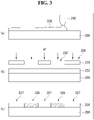
- FIG. 3 is a view illustrating sequential processes of a method for manufacturing a transparent conductive layer according to an embodiment of the present invention.
- a substrate 200 on which a transparent conductive layer is to be formed is prepared.
- the substrate 200 may be formed of various materials such as a resin film, a glass substrate, a metal substrate, and the like.
- the copper nanowire dispersion solution described above is prepared.
- a copper precursor and a nickel precursor are put into a flask, impurities are removed, and nanowires are formed at a temperature of about 200°C.
- a salt type precursor such as copper chloride, copper acetate, copper nitrate, or copper acetylacetonate may be used.
- a salt type precursor such as nickel chloride, nickel acetate, nickel nitrate, or nickel acetylacetonate may be used.
- a ratio of copper and nickel is beneficially 2:1. When the ratio of copper decreases or the ratio of nickel increases, a length of the wire is reduced. Conversely, when the ratio of copper increases or the ratio of nickel decreases, a length of the wire is increased.
- the temperature is lowered to room temperature, a cleaning is performed using a hexane, and it is left for 2 to 3 days.
- a binder is mixed with the solution to prepare a copper nanowire dispersion solution.
- An additive such as a dispersing agent or surfactant may be added to the copper nanowire dispersion solution.
- the prepared copper nanowire dispersion solution is put to a bar coater and applied to the substrate 200 through a bar coating method.
- a general solution application method such as a spin coating method or the like may be used, in addition to the bar coating method.
- the substrate 200 to which the copper nanowire dispersion solution has been applied is heated to remove the solvent.
- a mask 230 including a transmission portion 232 and a blocking portion 235 is disposed on a coating layer 222 formed by the copper nanowire dispersion solution.
- the transmission portion 232 is disposed to correspond to a portion of the coating layer 222 in which a conductive region is to be formed
- the blocking portion 235 is disposed to correspond to a portion of the coating layer 222 in which a non-conductive region is to be formed.
- a light in an infrared region is irradiated to the substrate 200.
- a range of irradiating light energy is higher than 30 J/cm 2 , preferably 35 ⁇ 100 J/cm 2 .
- a partial amount of light is irradiated to the substrate 200 through the transmission portion 232 of the mask 230, and a partial amount of light is blocked by the blocking portion 235 of the mask 230, rather than being irradiated to the substrate 200.
- the region to which light has not been irradiated is formed as a non-conductive region 227 is formed.
- the shells of the wires are removed and surfaces of the wires are melted and welded together, leading to a very high conductivity, which can be controlled by various factors such as the energy density of the irradiated light and the materials and thicknesses of the core and the shell(s).
- the non-conductive region 227 to which light has not been irradiated most of the shells of the wires are not removed, leading to insulating properties.
- some of the shells may be removed with the crossing wires being in contact with each other, leading to a very low conductivity.
- the transparent conductive film having the conductive region and the non-conductive region is formed without performing a physical patterning process, which can be used for manufacturing a display device in which the conductive region can be used as an electrode or a wiring.
- the copper nanowires manufactured according to Embodiment 1 described above were measured with SEM and TEM.
- the results of the SEM measurement are illustrated in FIGS. 4A through 4D
- the results of the TEM measurement are illustrated in FIG. 5 .
- copper wires having a length equal to or greater than 22 ⁇ m and a width equal to or greater than 0.04 ⁇ m were synthesized. Also, as shown in FIG. 5 , a copper oxide is present on a surface of the copper core.
- the copper nanowire dispersion solution prepared according to Embodiment 1 described above was applied to a substrate to form a coating film.
- a silver nanowire dispersion solution including silver nanowires including a silver (Ag) core and a PVP shell is applied to a substrate to form a coating film.
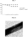
- the coating film manufactured according to Embodiment 2 of the present invention has a sheet resistance that decreases as an amount of light irradiated thereto increases, while the coating film manufactured according to Comparative Example 1 has a sheet resistance that rather increases as an amount of light irradiated thereto increases.
- the coating film manufactured according to Embodiment 2 of the present invention has the conductivity that increases as the amount of light irradiated thereto increases.
- the coating film manufactured according to Embodiment 2 of the present invention has a uniform transmittance although an amount of light irradiated thereto is increased, while the coating film manufactured according to Comparative Example 1 has a transmittance that is decreased to about 70% when an amount of light irradiated thereto is increased, and the transmittance is then maintained at the level.
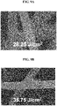
- FIGS. 8A through 8C a bond of the nanowire of the coating film manufactured according to Comparative Example 1 was broken when an amount of irradiated light was 33.25 J/cm 2 .
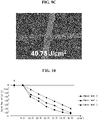
- FIGS. 9A through 9C the nanowires of the coating film manufactured according to Embodiment 2 come into contact with each other when an amount of irradiated light was 35.75 J/cm 2 , and the nanowires were welded and combined when an amount of irradiated light was 40.75 J/cm 2 .
- 0.1 wt% of copper nanowire manufactured according to Embodiment 1 described above, 98.5 wt% of Hexane as solvent, and 1.4 wt% of Oleylamine as other organic substances were mixed to prepare a copper nanowire dispersion solution.
- the copper nanowire dispersion solution was applied to a substrate to form a coating film.
- the transparent conductive layer including copper nanowires according to an embodiment of the present invention has an increased conductivity and excellent transmittance over an amount of irradiated light.
- the transparent conductive layer according to an embodiment of the present invention has reliable characteristics sufficient to be applied to a display device.
- Ethylene glycol (5 to 50 ml), silver (Ag) precursor (AgNO 3 ) and PVP(polyvinylpyrrolidone)((C 6 H 9 NO) x ) (molecular weight: 10,000 to 150,000) were put in a three neck distillation flask and dissolved into a solution at a predetermined ratio, and stabilized at high temperatures ranging from 150°C to 200°C. Copper chloride (CuCl 2 ) and sodium chloride (NaCl) were added at an appropriate ratio. The corresponding state was maintained for a predetermined period of time such that the silver nanowires were sufficiently grown to complete reaction.
- silver (Ag) precursor AgNO 3
- PVP(polyvinylpyrrolidone)((C 6 H 9 NO) x ) molethylene glycol
- CuCl 2 copper chloride
- NaCl sodium chloride
- the silver nanowires were washed with de-ionized (DI) water, ethanol, acetone, and the like, to remove impurities.
- DI de-ionized
- 3-glycidoxypropyltrimethoxysilane as a silane-based surfactant was mixed therewith and heated at temperatures ranging from 100°C to 120°C.
- the reaction was stopped and the nanowires were washed with DI water, ethanol, acetone, and the like, to remove impurities. Concentration was calculated to add ethanol or DI water and dispersed to synthesize silver nanowires.
- the silver nanowires manufactured according to Embodiment 6 were measured with an SEM as illustrated in FIG. 11 . As shown in FIG. 11 , the silver nanowires were synthesized.
- the silver nanowire dispersion solution prepared according to Embodiment 6 described above was applied to a substrate to form a coating film.
- the coating film formed according to Embodiment 7 of the present invention has a sheet resistance that decrease as an amount of light irradiated thereto increases, whereas the coating film formed according to Comparative Example 1 has a sheet resistance that rather increases as an amount of light irradiated thereto increases.
- the conductivity of the coating film formed according to Embodiment 7 of the present invention increases as the amount of light irradiated thereto increases.
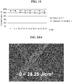
- the coating film formed according to Embodiment 7 of the present invention has a uniform transmittance, although the amount of light irradiated thereto is increased, whereas the coating film formed according to Comparative Example 1 has a transmittance that is decreased to about 70% when an amount of light irradiated thereto is increased, and the transmittance is then maintained at the level.
- the nanowires of the coating film manufactured according to Embodiment 7 come into contact when an amount of irradiated light was 30.75 J/cm 2 and the nanowires were welded and bonded together when an amount of irradiated light was 33.25 J/cm 2 .
- the silver nanowires manufactured according to Embodiment 6 was heat-treated for 30 minutes to 180 minutes under a high temperature condition of 200 °C.
- the silver nanowires manufactured according to Comparative Example 1 described above was heat-treated for 30 minutes under a high temperature condition of 200 °C.
- FIG. 15 A SEM image of the silver nanowire according to Comparative Example 2 described above is shown in FIG. 15 , and a SEM image of a silver nanowire according to Embodiment 8 is shown in FIGS. 16A and 16B .
- the copper nanowires and the silver nanowires according to embodiments of the present invention have excellent sheet resistance and conductivity characteristics, as well as an excellent heat resistance.
- FIG. 17 is a view illustrating a display device according to the first embodiment of the present invention
- FIG. 18 is a view illustrating a display device according to the second embodiment of the present invention
- FIG. 19 is a view illustrating a display device according to the third embodiment of the present invention.
- a display device may be a liquid crystal display (LCD) device 300.
- the LCD device 300 may include a TFT array substrate 310 and a color filter substrate 370 facing each other with a liquid crystal layer 360 interposed therebetween.
- the color filter substrate 370 includes a black matrix 375 demarcating each pixel, a color filter 380 formed in a pixel demarcated by the black matrix 375, and a common electrode 385 positioned on the color filter 380.
- R, G, and B color filters 380 are formed in pixel regions demarcated by the black matrix 375 to realize R, G, and B colors.
- An overcoat layer may be further provided between the color filter 380 and the common electrode 385.
- a gate electrode 315 is positioned on the TFT array substrate 310, and a gate insulating layer 320 is positioned on the gate electrode 315 to insulate the gate electrode 315.
- a semiconductor layer 325 corresponding to the gate electrode 315 is positioned on the gate insulating layer 320, and a source electrode 330a and a drain electrode 330b are positioned on both sides of the semiconductor layer 325 to form a thin film transistor (TFT).
- a protective layer 335 is positioned on the TFT, and a pixel electrode 340 connected to the drain electrode 330b is positioned on the protective layer 335.
- a vertical field is formed between the pixel electrode 340 to which a pixel signal is supplied through the TFT and the common electrode 385 to which a reference voltage is supplied, thus driving liquid crystal.
- a twisted-nematic (TN) LCD device in which the pixel electrode 340 is positioned on the TFT array substrate 310 and the common electrode 385 is positioned on the color filter substrate 370 is illustrated and described, but an IPS mode LCD device in which both a pixel electrode and a common electrode are formed on the TFT array substrate 310 may also be taken as an example.
- one or more of the pixel electrode 340 and the common electrode 385 may be formed as a transparent conductive layer formed with a nanowire dispersion solution.
- the pixel electrode 340 may have a conductive region 341 and a non-conductive region 342, and here, the conductive region 341 serves as an electrode, and the non-conductive region 342 serves as an insulating layer.
- the common electrode 385 entirely serves as a conductive region. Because a patterning process to form the pixel electrode and the common electrode can be omitted, a damage to the existing structure may be prevented and manufacturing cost may be reduced.
- a display device may be an organic light emitting display device.
- a gate electrode 415 is positioned on a substrate 410, and a gate insulating layer 420 is positioned on the gate electrode 415 in order to insulate the gate electrode 415.
- a semiconductor layer 425 corresponding to the gate electrode 415 is positioned on the gate insulating layer 420, and a source electrode 430a and a drain electrode 430b are positioned on both sides of the semiconductor layer 425 to form a TFT.
- a planarization layer 435 is positioned on the TFT, and a pixel electrode 440 connected to the drain electrode 430b is positioned on the planarization layer 435.
- a bank layer 445 is positioned on the pixel electrode 440 to expose a portion of the pixel electrode 440.
- An organic light emitting layer 450 is positioned on the pixel electrode 440 and the bank layer 445.
- the organic light emitting layer 450 a layer in which electrons and holes are combined to emit light, may include a hole injection layer, a hole transport layer, an electron transport layer, and an electron injection layer.
- a counter electrode 455 is positioned on the substrate 410 with the organic light emitting layer 450 formed thereon, forming the organic light emitting display device 400 according to the second embodiment of the present invention.
- the pixel electrode may be formed as a transparent conductive layer manufactured with a nanowire dispersion solution according to an embodiment of the present invention.
- the pixel electrode 440 may include a conductive region 441 and a non-conductive region 442, and here, the conductive region 441 serves as an electrode, and the non-conductive region 442 serves as an insulating layer.
- the organic light emitting display device 400 according to the second embodiment of the present invention since a patterning process to form the pixel electrode can be omitted, a damage to the existing structure may be prevented and manufacturing cost may be reduced.
- a display device may be a touch device.
- driving electrodes 520 and sensing electrodes 530 are disposed to sandwich a substrate 510, and a protective substrate 540 is positioned to protect these elements, thus forming the touch device 500.
- the driving electrodes 520 are connected on a lower surface of the substrate 510 in a first direction.
- the driving electrodes 520 may be formed to be close to each other in a regular pattern such as a diamond pattern on the lower surface of the substrate 510.
- the driving electrodes 520 positioned in a column having the same X coordinate are connected to each other to form a plurality of X patterns.
- the sensing electrodes 530 are formed on the substrate 510 in a second direction, and here, the sensing electrodes 530 are alternately disposed with respect to the driving electrodes 520 so as not to overlap the driving electrodes 520.
- the sensing electrodes 530 are formed to be close to each other in a diamond pattern, like the driving electrodes 520, and here, the sensing electrodes 530 positioned in a row having the same Y coordinate are connected to each other to form a plurality of Y patterns.
- the touch device 500 when a user's finger or an object comes into contact with an upper portion of the protective substrate 540, a change in capacitance of the driving electrode 520 and the sensing electrode 530 at the contact position is transmitted. As the change in capacitance is electrically converted by a touch recognition processor, or the like, the contact position is recognized and the display device operates.
- the driving electrodes 520 and the sensing electrodes 530 are beneficially formed of a transparent conductive material such that the light emitted from an underlying LCD device or organic light emitting display device can transmit therethrough.
- one or more of the driving electrodes 520 and the sensing electrodes 530 of the touch device 500 may be formed as a transparent conductive layer manufactured with a nanowire dispersion solution according to an embodiment of the present invention.
- each driving electrode 520 may include a conductive region 521 and a non-conductive region 522, and here, the conductive region 521 serves as an electrode, and the non-conductive region 522 serves as an insulating layer.
- each sensing electrode 530 may include a conductive region 531 and a non-conductive region 532, and here, the conductive region 531 serves as an electrode, and the non-conductive region 532 serves as an insulating layer.
- a transparent conductive layer according to an embodiment of the present invention may have a conductive region and a non-conductive region, and electrodes or wirings may be manufactured without performing a patterning process. As a result, a damage to the film due to its patterning process may be prevented, and thus, electrical characteristics of a display device in which the transparent conductive layer is formed may be enhanced, leading to an enhanced display quality.
- the process of manufacturing the transparent conductive layer may be simplified, with may reduce manufacturing cost and enhance productivity.
Landscapes
- Engineering & Computer Science (AREA)
- Physics & Mathematics (AREA)
- Theoretical Computer Science (AREA)
- General Engineering & Computer Science (AREA)
- General Physics & Mathematics (AREA)
- Optics & Photonics (AREA)
- Human Computer Interaction (AREA)
- Nonlinear Science (AREA)
- Crystallography & Structural Chemistry (AREA)
- Chemical & Material Sciences (AREA)
- Mathematical Physics (AREA)
- Manufacturing & Machinery (AREA)
- Non-Insulated Conductors (AREA)
Claims (11)
- Lichtdurchlässige leitfähige Schicht (228) für eine Anzeigevorrichtung (300), wobei die lichtdurchlässige leitfähige Schicht (228) durch ein Verfahren gebildet ist, das einen Schritt zum Bereitstellen von mehreren Nanodrähten (100) umfasst, wobei jeder Nanodraht (100) Folgendes umfasst:einen Kern (110), der ein Metall enthält,eine erste Schale (120) auf dem Kern (110), wobei die erste Schale (120) ein Oxid des Metalls der Schale (110) oder ein Polymermaterial enthält, undeine zweite Schale (130) auf der ersten Schale (120), wobei die zweite Schale (130) eine organische grenzflächenaktive Substanz enthält;dadurch gekennzeichnet, dass das Verfahren zum Bilden der lichtdurchlässigen leitfähigen Schicht (228) einen Schritt zum Bilden eines leitfähigen Bereichs (225) und eines nicht leitfähigen Bereichs (227) umfasst, wodurch ein lichtdurchlässiges leitfähiges Muster gebildet wird,wobei der leitfähige Bereich (225) gebildet wird, indem aufgrund von Oberflächenplasmonenresonanz durch Bestrahlen eines Bereichs der lichtdurchlässigen leitfähigen Schicht (228) mit Licht die Schalen (110, 120) der Nanodrähte dort, wo die Nanodrähte einander kreuzen, so dass die Oberflächen der Nanodrähte geschmolzen und zusammen geschweißt werden, teilweise entfernt werden, so dass die Kerne (110) von mindestens zwei der mehreren Nanodrähte (100) durch die erste Schale (120) und die zweite Schale (130) in Kontakt sind, undwobei der nicht leitfähige Bereich (227) in einem Bereich der lichtdurchlässigen leitfähigen Schicht (228) gebildet ist, der nicht bestrahlt worden ist.
- Lichtdurchlässige leitfähige Schicht (228) nach Anspruch 1, wobei das Metall Cu oder Ag ist.
- Lichtdurchlässige leitfähige Schicht (228) nach einem der vorhergehenden Ansprüche, wobei ein Aspektverhältnis der mehreren Nanodrähte im Bereich von 10 bis 10000 liegt.
- Lichtdurchlässige leitfähige Schicht (228) nach einem der vorhergehenden Ansprüche, wobei die Anzeigevorrichtung (300) eine Flüssigkristallanzeigevorrichtung (LCD-Vorrichtung), eine organische lichtemittierende Anzeigevorrichtung oder eine berührungsempfindliche Anzeigevorrichtung ist, die eine oder mehrere Elektroden enthält, die aus der lichtdurchlässigen leitfähigen Schicht gebildet sind.
- Anzeigevorrichtung, die eine lichtdurchlässige leitfähige Schicht nach einem der Ansprüche 1 bis 4 umfasst.
- Anzeigevorrichtung nach Anspruch 5, wobei die Anzeigevorrichtung (300) eine Flüssigkristallanzeigevorrichtung (LCD-Vorrichtung), eine organische lichtemittierende Anzeigevorrichtung oder eine berührungsempfindliche Anzeigevorrichtung ist, die eine oder mehrere Elektroden enthält, die aus der lichtdurchlässigen leitfähigen Schicht gebildet sind.
- Verfahren zum Herstellen einer lichtdurchlässigen leitfähigen Schicht (228) für eine Anzeigevorrichtung (300), wobei die lichtdurchlässige leitfähige Schicht (228) mehrere Nanodrähte enthält und einen leitfähigen Bereich (225) und einen nicht leitfähigen Bereich (227) umfasst, die ein lichtdurchlässiges leitfähiges Muster bilden, wobei das Verfahren Folgendes umfasst:Bereitstellen einer Dispersionslösung aus Metall-Nanodrähten, wobei der Nanodraht einen Kern (110), der ein Metall enthält, eine erste Schale (120) auf dem Kern (110) und eine zweite Schale (130) auf der ersten Schale (120) enthält, wobei die erste Schale (120) ein Oxid des Metalls des Kerns (110) oder ein Polymermaterial enthält und die zweite Schale (130) eine organische grenzflächenaktive Substanz enthält,Aufbringen der Dispersionslösung aus Metall-Nanodrähten auf ein Substrat (200);Erwärmen des Substrats (200), auf der die Dispersionslösung aus Nanodrähten aufgebracht ist, um eine Schicht aus Metall-Nanodrähten zu bilden, undEinstrahlen von Licht auf die Schicht aus Metall-Nanodrähten, so dass die Schalen der Nanodrähte aufgrund von Oberflächenplasmonenresonanz teilweise entfernt werden, wobei die Nanodrähte einander kreuzen und Oberflächen der Nanodrähte in einem Bereich der Schicht aus Metall-Nanodrähten, der bestrahlt wird, um den leitfähigen Bereich (225) zu bilden, geschmolzen werden, wobei die Kerne (110) von mindestens zwei Nanodrähten (100) in dem leitfähigen Bereich (225) durch die erste Schale (120) und die zweite Schale (130) miteinander in Kontakt sind;wobei ein Bereich der Schicht aus Metall-Nanodrähten, der nicht bestrahlt worden ist, den nicht leitfähigen Bereich (227) bildet und wobei der leitfähige und der nicht leitfähige Bereich (225, 227) das lichtdurchlässige leitfähige Muster der lichtdurchlässigen leitfähigen Schicht (228) bilden.
- Verfahren nach Anspruch 7, wobei das Licht durch eine Maske eingestrahlt wird, die einen durchlässigen Abschnitt und einen blockierenden Abschnitt aufweist.
- Verfahren nach Anspruch 8, wobei die Schicht aus Metall-Nanodrähten, die mit dem Licht durch den durchlässigen Abschnitt bestrahlt wird, der leitfähige Bereich (225) wird.
- Verfahren nach einem der Ansprüche 7 bis 9, wobei das Substrat ein biegsames Substrat ist.
- Verfahren nach einem der vorhergehenden Ansprüche 7 bis 10, wobei die Anzeigevorrichtung (300) eine Flüssigkristallanzeigevorrichtung, eine organische lichtemittierende Anzeigevorrichtung oder eine berührungsempfindliche Anzeigevorrichtung ist.
Applications Claiming Priority (2)
| Application Number | Priority Date | Filing Date | Title |
|---|---|---|---|
| KR20140081276 | 2014-06-30 | ||
| KR1020140181849A KR102356158B1 (ko) | 2014-06-30 | 2014-12-16 | 투명도전막의 제조방법 및 투명도전막을 포함하는 표시장치 |
Publications (2)
| Publication Number | Publication Date |
|---|---|
| EP2963462A1 EP2963462A1 (de) | 2016-01-06 |
| EP2963462B1 true EP2963462B1 (de) | 2022-10-12 |
Family
ID=53496553
Family Applications (1)
| Application Number | Title | Priority Date | Filing Date |
|---|---|---|---|
| EP15174597.3A Active EP2963462B1 (de) | 2014-06-30 | 2015-06-30 | Transparente, leitfähige schicht, verfahren zur herstellung davon und anzeigevorrichtung damit |
Country Status (3)
| Country | Link |
|---|---|
| US (1) | US10627932B2 (de) |
| EP (1) | EP2963462B1 (de) |
| CN (1) | CN105225727B (de) |
Families Citing this family (3)
| Publication number | Priority date | Publication date | Assignee | Title |
|---|---|---|---|---|
| CN105320330B (zh) * | 2014-07-29 | 2018-09-14 | 南京瀚宇彩欣科技有限责任公司 | 光电调变堆叠 |
| US9942979B2 (en) * | 2014-11-03 | 2018-04-10 | Samsung Electronics Co., Ltd. | Flexible printed circuit board |
| CN107102774A (zh) * | 2017-05-04 | 2017-08-29 | 重庆市大渃科技有限公司 | 新型电容式触摸屏及其生产方法 |
Citations (1)
| Publication number | Priority date | Publication date | Assignee | Title |
|---|---|---|---|---|
| US20090188697A1 (en) * | 2008-01-28 | 2009-07-30 | Honeywell International, Inc. | Transparent conductors and methods for fabricating transparent conductors |
Family Cites Families (8)
| Publication number | Priority date | Publication date | Assignee | Title |
|---|---|---|---|---|
| US20030066998A1 (en) * | 2001-08-02 | 2003-04-10 | Lee Howard Wing Hoon | Quantum dots of Group IV semiconductor materials |
| US20060044299A1 (en) * | 2004-08-31 | 2006-03-02 | Jian Wang | System and method for compensating for a fabrication artifact in an electronic device |
| SG150516A1 (en) * | 2005-08-12 | 2009-03-30 | Cambrios Technologies Corp | Nanowires-based transparent conductors |
| TWI307646B (en) * | 2005-12-06 | 2009-03-21 | Lg Chemical Ltd | Core-shell type nanoparticles and method for preparing the same |
| US8940194B2 (en) * | 2010-08-20 | 2015-01-27 | The Board Of Trustees Of The Leland Stanford Junior University | Electrodes with electrospun fibers |
| KR101940591B1 (ko) * | 2012-02-16 | 2019-01-21 | 오꾸라 고교 가부시키가이샤 | 투명 도전 기재의 제조 방법 및 투명 도전 기재 |
| KR101324281B1 (ko) * | 2012-03-15 | 2013-11-01 | 인하대학교 산학협력단 | 고유연성을 가지는 산화 그라핀/은 나노와이어 하이브리드를 기반으로 하는 투명전도성 필름 |
| US9920207B2 (en) * | 2012-06-22 | 2018-03-20 | C3Nano Inc. | Metal nanostructured networks and transparent conductive material |
-
2015
- 2015-06-24 CN CN201510355346.8A patent/CN105225727B/zh active Active
- 2015-06-29 US US14/753,715 patent/US10627932B2/en active Active
- 2015-06-30 EP EP15174597.3A patent/EP2963462B1/de active Active
Patent Citations (1)
| Publication number | Priority date | Publication date | Assignee | Title |
|---|---|---|---|---|
| US20090188697A1 (en) * | 2008-01-28 | 2009-07-30 | Honeywell International, Inc. | Transparent conductors and methods for fabricating transparent conductors |
Also Published As
| Publication number | Publication date |
|---|---|
| US10627932B2 (en) | 2020-04-21 |
| CN105225727A (zh) | 2016-01-06 |
| EP2963462A1 (de) | 2016-01-06 |
| US20150378489A1 (en) | 2015-12-31 |
| CN105225727B (zh) | 2017-06-09 |
Similar Documents
| Publication | Publication Date | Title |
|---|---|---|
| US9307633B2 (en) | Conductive structure, touch panel, and method for manufacturing same | |
| CN107039098B (zh) | 银纳米线的群、其制造方法、包括其的电导体和电子装置 | |
| US6630980B2 (en) | Transparent flexible barrier for liquid crystal display devices and method of making the same | |
| US8520183B2 (en) | Display substrate, liquid crystal display including the display substrate, and method of manufacturing the display substrate | |
| KR20170107309A (ko) | 도전체, 그 제조 방법, 및 이를 포함하는 전자 소자 | |
| EP3734620B1 (de) | Verfahren zur herstellung einer transparenten elektrode | |
| TWI396910B (zh) | 顯示基板、顯示基板製造方法及具有該顯示基板之顯示面板 | |
| KR101809296B1 (ko) | 투명전극 및 이를 포함하는 전자 소자 | |
| KR20170075507A (ko) | 전도성 소자 및 이를 포함하는 전자 소자 | |
| US10627932B2 (en) | Transparent conductive layer, method for manufacturing the same and display device including the same | |
| US20170003808A1 (en) | Transparent conductor, method of fabricating the same and optical display including the same | |
| KR20020066573A (ko) | 횡전계형 액정표시장치용 하부 기판 및 그의 제조방법 | |
| US9933655B2 (en) | Polarizer and display device comprising the same | |
| KR101492538B1 (ko) | 박막 트랜지스터 기판 및 이의 제조 방법 | |
| US20180157087A1 (en) | Transparent conductive film and liquid crystal display (lcd) comprising the same | |
| JPH10241464A (ja) | 透明導電膜付き基体とその製造方法 | |
| CN213122931U (zh) | 触控面板及触控装置 | |
| US20170349481A1 (en) | Transparent conductor comprising metal nanowires, and method for forming the same | |
| WO2018211910A1 (ja) | 透明導電性フィルムおよび画像表示装置 | |
| KR102219551B1 (ko) | 투명 전극 | |
| KR102356158B1 (ko) | 투명도전막의 제조방법 및 투명도전막을 포함하는 표시장치 | |
| JP2022086460A (ja) | エレクトロクロミック素子及びエレクトロクロミック調光レンズ | |
| JPH10208554A (ja) | 透明導電膜及びそれを用いた液晶素子 | |
| CN114089854A (zh) | 触控面板、触控面板的制作方法及触控装置 | |
| KR101756372B1 (ko) | 고종횡비를 갖는 금속 나노선 및 이의 제조 방법 |
Legal Events
| Date | Code | Title | Description |
|---|---|---|---|
| PUAI | Public reference made under article 153(3) epc to a published international application that has entered the european phase |
Free format text: ORIGINAL CODE: 0009012 |
|
| AK | Designated contracting states |
Kind code of ref document: A1 Designated state(s): AL AT BE BG CH CY CZ DE DK EE ES FI FR GB GR HR HU IE IS IT LI LT LU LV MC MK MT NL NO PL PT RO RS SE SI SK SM TR |
|
| AX | Request for extension of the european patent |
Extension state: BA ME |
|
| 17P | Request for examination filed |
Effective date: 20160608 |
|
| RBV | Designated contracting states (corrected) |
Designated state(s): AL AT BE BG CH CY CZ DE DK EE ES FI FR GB GR HR HU IE IS IT LI LT LU LV MC MK MT NL NO PL PT RO RS SE SI SK SM TR |
|
| STAA | Information on the status of an ep patent application or granted ep patent |
Free format text: STATUS: EXAMINATION IS IN PROGRESS |
|
| 17Q | First examination report despatched |
Effective date: 20181113 |
|
| GRAP | Despatch of communication of intention to grant a patent |
Free format text: ORIGINAL CODE: EPIDOSNIGR1 |
|
| STAA | Information on the status of an ep patent application or granted ep patent |
Free format text: STATUS: GRANT OF PATENT IS INTENDED |
|
| INTG | Intention to grant announced |
Effective date: 20220224 |
|
| RAP3 | Party data changed (applicant data changed or rights of an application transferred) |
Owner name: LG DISPLAY CO., LTD. |
|
| GRAJ | Information related to disapproval of communication of intention to grant by the applicant or resumption of examination proceedings by the epo deleted |
Free format text: ORIGINAL CODE: EPIDOSDIGR1 |
|
| STAA | Information on the status of an ep patent application or granted ep patent |
Free format text: STATUS: EXAMINATION IS IN PROGRESS |
|
| INTC | Intention to grant announced (deleted) | ||
| GRAP | Despatch of communication of intention to grant a patent |
Free format text: ORIGINAL CODE: EPIDOSNIGR1 |
|
| STAA | Information on the status of an ep patent application or granted ep patent |
Free format text: STATUS: GRANT OF PATENT IS INTENDED |
|
| INTG | Intention to grant announced |
Effective date: 20220812 |
|
| GRAS | Grant fee paid |
Free format text: ORIGINAL CODE: EPIDOSNIGR3 |
|
| GRAA | (expected) grant |
Free format text: ORIGINAL CODE: 0009210 |
|
| STAA | Information on the status of an ep patent application or granted ep patent |
Free format text: STATUS: THE PATENT HAS BEEN GRANTED |
|
| AK | Designated contracting states |
Kind code of ref document: B1 Designated state(s): AL AT BE BG CH CY CZ DE DK EE ES FI FR GB GR HR HU IE IS IT LI LT LU LV MC MK MT NL NO PL PT RO RS SE SI SK SM TR |
|
| REG | Reference to a national code |
Ref country code: GB Ref legal event code: FG4D |
|
| REG | Reference to a national code |
Ref country code: CH Ref legal event code: EP |
|
| REG | Reference to a national code |
Ref country code: DE Ref legal event code: R096 Ref document number: 602015081134 Country of ref document: DE |
|
| REG | Reference to a national code |
Ref country code: IE Ref legal event code: FG4D |
|
| REG | Reference to a national code |
Ref country code: AT Ref legal event code: REF Ref document number: 1524506 Country of ref document: AT Kind code of ref document: T Effective date: 20221115 |
|
| REG | Reference to a national code |
Ref country code: LT Ref legal event code: MG9D |
|
| REG | Reference to a national code |
Ref country code: NL Ref legal event code: MP Effective date: 20221012 |
|
| REG | Reference to a national code |
Ref country code: AT Ref legal event code: MK05 Ref document number: 1524506 Country of ref document: AT Kind code of ref document: T Effective date: 20221012 |
|
| PG25 | Lapsed in a contracting state [announced via postgrant information from national office to epo] |
Ref country code: NL Free format text: LAPSE BECAUSE OF FAILURE TO SUBMIT A TRANSLATION OF THE DESCRIPTION OR TO PAY THE FEE WITHIN THE PRESCRIBED TIME-LIMIT Effective date: 20221012 |
|
| PG25 | Lapsed in a contracting state [announced via postgrant information from national office to epo] |
Ref country code: SE Free format text: LAPSE BECAUSE OF FAILURE TO SUBMIT A TRANSLATION OF THE DESCRIPTION OR TO PAY THE FEE WITHIN THE PRESCRIBED TIME-LIMIT Effective date: 20221012 Ref country code: PT Free format text: LAPSE BECAUSE OF FAILURE TO SUBMIT A TRANSLATION OF THE DESCRIPTION OR TO PAY THE FEE WITHIN THE PRESCRIBED TIME-LIMIT Effective date: 20230213 Ref country code: NO Free format text: LAPSE BECAUSE OF FAILURE TO SUBMIT A TRANSLATION OF THE DESCRIPTION OR TO PAY THE FEE WITHIN THE PRESCRIBED TIME-LIMIT Effective date: 20230112 Ref country code: LT Free format text: LAPSE BECAUSE OF FAILURE TO SUBMIT A TRANSLATION OF THE DESCRIPTION OR TO PAY THE FEE WITHIN THE PRESCRIBED TIME-LIMIT Effective date: 20221012 Ref country code: FI Free format text: LAPSE BECAUSE OF FAILURE TO SUBMIT A TRANSLATION OF THE DESCRIPTION OR TO PAY THE FEE WITHIN THE PRESCRIBED TIME-LIMIT Effective date: 20221012 Ref country code: ES Free format text: LAPSE BECAUSE OF FAILURE TO SUBMIT A TRANSLATION OF THE DESCRIPTION OR TO PAY THE FEE WITHIN THE PRESCRIBED TIME-LIMIT Effective date: 20221012 Ref country code: AT Free format text: LAPSE BECAUSE OF FAILURE TO SUBMIT A TRANSLATION OF THE DESCRIPTION OR TO PAY THE FEE WITHIN THE PRESCRIBED TIME-LIMIT Effective date: 20221012 |
|
| PG25 | Lapsed in a contracting state [announced via postgrant information from national office to epo] |
Ref country code: RS Free format text: LAPSE BECAUSE OF FAILURE TO SUBMIT A TRANSLATION OF THE DESCRIPTION OR TO PAY THE FEE WITHIN THE PRESCRIBED TIME-LIMIT Effective date: 20221012 Ref country code: PL Free format text: LAPSE BECAUSE OF FAILURE TO SUBMIT A TRANSLATION OF THE DESCRIPTION OR TO PAY THE FEE WITHIN THE PRESCRIBED TIME-LIMIT Effective date: 20221012 Ref country code: LV Free format text: LAPSE BECAUSE OF FAILURE TO SUBMIT A TRANSLATION OF THE DESCRIPTION OR TO PAY THE FEE WITHIN THE PRESCRIBED TIME-LIMIT Effective date: 20221012 Ref country code: IS Free format text: LAPSE BECAUSE OF FAILURE TO SUBMIT A TRANSLATION OF THE DESCRIPTION OR TO PAY THE FEE WITHIN THE PRESCRIBED TIME-LIMIT Effective date: 20230212 Ref country code: HR Free format text: LAPSE BECAUSE OF FAILURE TO SUBMIT A TRANSLATION OF THE DESCRIPTION OR TO PAY THE FEE WITHIN THE PRESCRIBED TIME-LIMIT Effective date: 20221012 Ref country code: GR Free format text: LAPSE BECAUSE OF FAILURE TO SUBMIT A TRANSLATION OF THE DESCRIPTION OR TO PAY THE FEE WITHIN THE PRESCRIBED TIME-LIMIT Effective date: 20230113 |
|
| REG | Reference to a national code |
Ref country code: DE Ref legal event code: R097 Ref document number: 602015081134 Country of ref document: DE |
|
| PG25 | Lapsed in a contracting state [announced via postgrant information from national office to epo] |
Ref country code: SM Free format text: LAPSE BECAUSE OF FAILURE TO SUBMIT A TRANSLATION OF THE DESCRIPTION OR TO PAY THE FEE WITHIN THE PRESCRIBED TIME-LIMIT Effective date: 20221012 Ref country code: RO Free format text: LAPSE BECAUSE OF FAILURE TO SUBMIT A TRANSLATION OF THE DESCRIPTION OR TO PAY THE FEE WITHIN THE PRESCRIBED TIME-LIMIT Effective date: 20221012 Ref country code: EE Free format text: LAPSE BECAUSE OF FAILURE TO SUBMIT A TRANSLATION OF THE DESCRIPTION OR TO PAY THE FEE WITHIN THE PRESCRIBED TIME-LIMIT Effective date: 20221012 Ref country code: DK Free format text: LAPSE BECAUSE OF FAILURE TO SUBMIT A TRANSLATION OF THE DESCRIPTION OR TO PAY THE FEE WITHIN THE PRESCRIBED TIME-LIMIT Effective date: 20221012 Ref country code: CZ Free format text: LAPSE BECAUSE OF FAILURE TO SUBMIT A TRANSLATION OF THE DESCRIPTION OR TO PAY THE FEE WITHIN THE PRESCRIBED TIME-LIMIT Effective date: 20221012 |
|
| PLBE | No opposition filed within time limit |
Free format text: ORIGINAL CODE: 0009261 |
|
| STAA | Information on the status of an ep patent application or granted ep patent |
Free format text: STATUS: NO OPPOSITION FILED WITHIN TIME LIMIT |
|
| PG25 | Lapsed in a contracting state [announced via postgrant information from national office to epo] |
Ref country code: SK Free format text: LAPSE BECAUSE OF FAILURE TO SUBMIT A TRANSLATION OF THE DESCRIPTION OR TO PAY THE FEE WITHIN THE PRESCRIBED TIME-LIMIT Effective date: 20221012 Ref country code: AL Free format text: LAPSE BECAUSE OF FAILURE TO SUBMIT A TRANSLATION OF THE DESCRIPTION OR TO PAY THE FEE WITHIN THE PRESCRIBED TIME-LIMIT Effective date: 20221012 |
|
| 26N | No opposition filed |
Effective date: 20230713 |
|
| PG25 | Lapsed in a contracting state [announced via postgrant information from national office to epo] |
Ref country code: SI Free format text: LAPSE BECAUSE OF FAILURE TO SUBMIT A TRANSLATION OF THE DESCRIPTION OR TO PAY THE FEE WITHIN THE PRESCRIBED TIME-LIMIT Effective date: 20221012 |
|
| PG25 | Lapsed in a contracting state [announced via postgrant information from national office to epo] |
Ref country code: MC Free format text: LAPSE BECAUSE OF FAILURE TO SUBMIT A TRANSLATION OF THE DESCRIPTION OR TO PAY THE FEE WITHIN THE PRESCRIBED TIME-LIMIT Effective date: 20221012 |
|
| PG25 | Lapsed in a contracting state [announced via postgrant information from national office to epo] |
Ref country code: MC Free format text: LAPSE BECAUSE OF FAILURE TO SUBMIT A TRANSLATION OF THE DESCRIPTION OR TO PAY THE FEE WITHIN THE PRESCRIBED TIME-LIMIT Effective date: 20221012 |
|
| REG | Reference to a national code |
Ref country code: CH Ref legal event code: PL |
|
| REG | Reference to a national code |
Ref country code: BE Ref legal event code: MM Effective date: 20230630 |
|
| PG25 | Lapsed in a contracting state [announced via postgrant information from national office to epo] |
Ref country code: LU Free format text: LAPSE BECAUSE OF NON-PAYMENT OF DUE FEES Effective date: 20230630 |
|
| REG | Reference to a national code |
Ref country code: IE Ref legal event code: MM4A |
|
| PG25 | Lapsed in a contracting state [announced via postgrant information from national office to epo] |
Ref country code: LU Free format text: LAPSE BECAUSE OF NON-PAYMENT OF DUE FEES Effective date: 20230630 |
|
| PG25 | Lapsed in a contracting state [announced via postgrant information from national office to epo] |
Ref country code: IE Free format text: LAPSE BECAUSE OF NON-PAYMENT OF DUE FEES Effective date: 20230630 |
|
| PG25 | Lapsed in a contracting state [announced via postgrant information from national office to epo] |
Ref country code: IE Free format text: LAPSE BECAUSE OF NON-PAYMENT OF DUE FEES Effective date: 20230630 Ref country code: CH Free format text: LAPSE BECAUSE OF NON-PAYMENT OF DUE FEES Effective date: 20230630 |
|
| PG25 | Lapsed in a contracting state [announced via postgrant information from national office to epo] |
Ref country code: IT Free format text: LAPSE BECAUSE OF FAILURE TO SUBMIT A TRANSLATION OF THE DESCRIPTION OR TO PAY THE FEE WITHIN THE PRESCRIBED TIME-LIMIT Effective date: 20221012 Ref country code: BE Free format text: LAPSE BECAUSE OF NON-PAYMENT OF DUE FEES Effective date: 20230630 |
|
| PG25 | Lapsed in a contracting state [announced via postgrant information from national office to epo] |
Ref country code: BG Free format text: LAPSE BECAUSE OF FAILURE TO SUBMIT A TRANSLATION OF THE DESCRIPTION OR TO PAY THE FEE WITHIN THE PRESCRIBED TIME-LIMIT Effective date: 20221012 |
|
| PG25 | Lapsed in a contracting state [announced via postgrant information from national office to epo] |
Ref country code: BG Free format text: LAPSE BECAUSE OF FAILURE TO SUBMIT A TRANSLATION OF THE DESCRIPTION OR TO PAY THE FEE WITHIN THE PRESCRIBED TIME-LIMIT Effective date: 20221012 |
|
| PGFP | Annual fee paid to national office [announced via postgrant information from national office to epo] |
Ref country code: DE Payment date: 20250422 Year of fee payment: 11 |
|
| PGFP | Annual fee paid to national office [announced via postgrant information from national office to epo] |
Ref country code: GB Payment date: 20250422 Year of fee payment: 11 |
|
| PGFP | Annual fee paid to national office [announced via postgrant information from national office to epo] |
Ref country code: FR Payment date: 20250422 Year of fee payment: 11 |
|
| PG25 | Lapsed in a contracting state [announced via postgrant information from national office to epo] |
Ref country code: CY Free format text: LAPSE BECAUSE OF FAILURE TO SUBMIT A TRANSLATION OF THE DESCRIPTION OR TO PAY THE FEE WITHIN THE PRESCRIBED TIME-LIMIT; INVALID AB INITIO Effective date: 20150630 |
|
| PG25 | Lapsed in a contracting state [announced via postgrant information from national office to epo] |
Ref country code: HU Free format text: LAPSE BECAUSE OF FAILURE TO SUBMIT A TRANSLATION OF THE DESCRIPTION OR TO PAY THE FEE WITHIN THE PRESCRIBED TIME-LIMIT; INVALID AB INITIO Effective date: 20150630 |
|
| PG25 | Lapsed in a contracting state [announced via postgrant information from national office to epo] |
Ref country code: TR Free format text: LAPSE BECAUSE OF FAILURE TO SUBMIT A TRANSLATION OF THE DESCRIPTION OR TO PAY THE FEE WITHIN THE PRESCRIBED TIME-LIMIT Effective date: 20221012 |