EP2957982A1 - Self-synchronizable network - Google Patents
Self-synchronizable network Download PDFInfo
- Publication number
- EP2957982A1 EP2957982A1 EP14173279.2A EP14173279A EP2957982A1 EP 2957982 A1 EP2957982 A1 EP 2957982A1 EP 14173279 A EP14173279 A EP 14173279A EP 2957982 A1 EP2957982 A1 EP 2957982A1
- Authority
- EP
- European Patent Office
- Prior art keywords
- node
- time
- network
- synchronization signal
- continuous synchronization
- Prior art date
- Legal status (The legal status is an assumption and is not a legal conclusion. Google has not performed a legal analysis and makes no representation as to the accuracy of the status listed.)
- Granted
Links
Images





Classifications
-
- G—PHYSICS
- G06—COMPUTING OR CALCULATING; COUNTING
- G06F—ELECTRIC DIGITAL DATA PROCESSING
- G06F1/00—Details not covered by groups G06F3/00 - G06F13/00 and G06F21/00
- G06F1/04—Generating or distributing clock signals or signals derived directly therefrom
- G06F1/12—Synchronisation of different clock signals provided by a plurality of clock generators
-
- H—ELECTRICITY
- H04—ELECTRIC COMMUNICATION TECHNIQUE
- H04L—TRANSMISSION OF DIGITAL INFORMATION, e.g. TELEGRAPHIC COMMUNICATION
- H04L7/00—Arrangements for synchronising receiver with transmitter
- H04L7/02—Speed or phase control by the received code signals, the signals containing no special synchronisation information
- H04L7/033—Speed or phase control by the received code signals, the signals containing no special synchronisation information using the transitions of the received signal to control the phase of the synchronising-signal-generating means, e.g. using a phase-locked loop
Definitions
- the present invention relates to a synchronizable network.
- the present invention specifically relates to clock distribution and self-organized synchronization in large scale networks, like high performance Multiprocessor System-on-Chips (MPSoCs) architectures.
- MPSoCs Multiprocessor System-on-Chips
- MPSoCs have become a key component for modern communications and computation systems. Lately, the trend to integrate more and more processing cores in a single silicon die has gained momentum, aided by promising benefits in mechanical footprint, computational performance, energy and cost efficiency. Hence, increasing the number of cores directly translates into high performance through parallel processing and high efficiency compared to single-core solutions.
- GALS globally asynchronous locally synchronous
- a globally synchronous design as shown in Fig. 1 where all cores 12 of a clocking network 11 share one master clock 13, is used.
- the communication latencies between cores are drastically reduced compared to GALS clocking.
- a very large chip area has to be clocked synchronously.
- the clock signals within MPSoCs have to be transmitted over ranges of some millimeters, which is a well-known bottleneck for speed, power and reliability.
- traditional globally synchronous clocking circuits have become too difficult for large MPSoCs with many cores, constantly growing chip size and wire induced delays.
- the clock trees consume a significant amount of power which is critical for mobile communication systems.
- Another strategy for network synchronization and clock distribution relates to self-organized synchronization of distributed network nodes in absence of an entraining master clock.
- Mutually connected phase-locked loop networks dynamical models and design parameters
- F.M. Orsatti, R. Carareto, J.R.C. Piqueira, IET Circuit Devices Syst.,2008, Vol. 2, No. 6, pp. 495-508 relates to distributing clock signals by using mutually connected architectures instead of master-slave type architectures.
- Mutually connected digital PLL networks are studied and conditions for the existence of synchronized states are derived, depending on individual node parameters and network connectivity, considering that the nodes are nonlinear oscillators with nonlinear coupling conditions.
- WO 2013/178237 A1 relates to a communication network of interconnected communication nodes, each node comprising an oscillator that is mutually coupled to oscillators of other communication nodes.
- the oscillator generates periodic synchronization pulses.
- the communication node further comprises a transmitter for transmitting the synchronization pulses to other communication nodes; a receiver for receiving synchronization pulses from other communication nodes; and a synchronization unit for synchronizing the phase of the synchronization pulses generated by the oscillator with the phase of the synchronization pulses received from other communication nodes by adjusting the phase of the synchronization pulses generated by the oscillator upon receipt of synchronization pulses from other communication nodes.
- the synchronization unit adjusts the phase of the synchronization pulses generated by the oscillator in such a way that a guaranteed network-wide synchronization is achieved for all communication nodes of the communication network.
- WO 2013/178237 A1 explicitly limits a transmission time delay of the synchronization pulses between the communication nodes to one eighth of the period of the oscillator.
- this disclosure does not provide a suitable solution for networks exhibiting a transmission time delay exceeding one eighth of the period of the oscillator, e.g., highly integrated chip networks.
- this solution assumes pulse coupling. Stochastic synchronization pulse emission is required to guarantee synchronization.
- this solution is not suitable for clock distributions with time-continuous coupling.
- This objective is achieved with a node according to the independent apparatus claim and a method for synchronizing a network according to the independent method claim.
- the present invention relates to a node for a network comprising a plurality of interconnected nodes.
- the node comprises a controllable oscillator generating a time-continuous synchronization signal for synchronizing the plurality of interconnected nodes of the network.
- the node further comprises a controller for comparing and synchronizing a phase of the time-continuous synchronization signal generated by the controllable oscillator, which is transmitted to another node of the network, with the phase of an external time-continuous synchronization signal received from the other node of the network by adjusting a frequency of the time-continuous synchronization signal generated by the controllable oscillator.
- the external time-continuous synchronization signal received from the other node of the network is delayed with respect to the time-continuous synchronization signal transmitted by the other node by a total time delay.
- the total time delay may be a transmission time delay resulting from a transmission time between the transmission of the external time-continuous synchronization signal by the other node and the following receipt of the external time-continuous synchronization signal by the node.
- the total time delay may also comprise any tunable additional time delays in addition to the transmission time delay.
- the controller iteratively adjusts the frequency of the time-continuous synchronization signal generated by the controllable oscillator such that a network-wide synchronization of oscillators is achieved for all nodes of the network. The synchronization is thus achieved in a continuous self-organized process in interaction with the other node of the network.
- the controller may be any control system with feedback of the continuous synchronization signal generated by the tunable oscillator.
- the controller in combination with the controllable oscillator may form a phase locked loop (PLL).
- PLLs are electronic components able to synchronize their synchronization signals by evaluating mutual phase differences and adjusting their frequencies accordingly.
- the controller then comprises a phase detector (PD) and a loop filter (LF).
- the controllable oscillator may be a voltage controlled oscillator (VCO).
- the phase detector compares the phase of the external time-continuous synchronization signal with the phase of the time-continuous synchronization signal generated by the controllable oscillator.
- a model for mutually coupled PLLs is described below using an analog PLL as an example.
- the present invention is not restricted to analog PLLs.
- the phase detector multiplies an external input signal x l with the output signal x k of the VCO.
- Total time delays, for example resulting from transmission time delays and/or tunable additional time delays between the PLLs are accounted for by a delay ⁇ T of the received signal.
- a feedback delay between the VCO and the PD is accounted for by a delay ⁇ f in the VCO signal. However, the feedback delay may be zero.
- the output x k C of the LF yields the control signal for the VCO.
- the first term containing a phase difference describes low frequency components of the signal, while the second term containing a sum of phases describes high frequency components. Approximating the LF as ideal, these high frequency components are fully damped and can therefore be omitted.
- K K VCO /2 is the coupling strength and has the dimension of a frequency.
- the cosine function containing the phase difference is called the coupling function. This is a closed phase equation for two mutually delay-coupled PLLs.
- Eq. (5) can be extended to a phase model for N delay coupled PLLs with transmission delays between coupled oscillators.
- a standard state-of-the-art PLL handles only a single input signal.
- the controller then compares and synchronizes a phase of the time-continuous synchronization signal generated by the controllable oscillator with the phases of external time-continuous synchronization signals received from a plurality of other nodes of the network by adjusting a frequency of the time-continuous synchronization signal generated by the controllable oscillator.
- One aspect of the present invention relates to a combiner for combining external time-continuous synchronization signals received from other nodes of the network to generate a combined external time-continuous synchronization signal.
- the phase detector compares the phase of the time-continuous synchronization signal generated by the controllable oscillator with the phase of the combined external time-continuous synchronization signal.
- the combiner may be part of the phase detector (PD).
- the combiner may be a non-inverting adder.
- the phase detector (PD) may be a multiplier for analog signals or an XOR gate for digital signals.
- the phase detector may compare the phase of the time-continuous synchronization signal generated by the controllable oscillator with the phase of each external time-continuous synchronization signal individually to generate a plurality of phase detector signals.
- the combiner then combines the phase detector signals to control the controllable oscillator.
- One aspect of the present invention relates to tuning the total time delay between mutually coupled PLLs.
- a stable in-phase synchronized solution, Eq. (8), with global frequency ⁇ cannot be achieved for arbitrary total time delays between coupled synchronizers.
- the total time delay is a design parameter and can be tuned by an additional delayer and the design of the network.
- a node may comprise a delayer for inducing an additional time delay to a transmission time delay.
- the total time delay effectively induces a frequency-dependent phase shift to a synchronization signal and, if appropriately tuned, changes the coupling properties such that stable synchronized states become possible.
- a delayer may be any means suitable to induce such phase shifts. The delayer may need to be specifically tuned for each input path.
- the total time delay may comprise a period of the controllable oscillator. Specifically, it may exceed one eighth of a period of the controllable oscillator.
- the node may further comprise a feedback delayer for inducing a feedback delay ⁇ f in a feedback path between the controllable oscillator and the phase detector.
- the feedback delay may compensate for the total time delay.
- the collective frequency then depends on the difference between the total time delay and the feedback delay.
- the total time delay may be tuned such that it minimizes a perturbation response rate ⁇ in order to arrive at an in-phase synchronized state with maximum stability as will be explained.
- the total time delay ⁇ T in combination with the feedback delay ⁇ f may be tuned such that a maximum perturbation decay can be achieved by optimizing the perturbation response rate ⁇ , see Eq. (9).
- further design parameters for optimizing the perturbation response rate ⁇ are the free running frequency ⁇ of the controllable oscillator, the coupling strength K , and the impulse response p ( u ) of a filter within the controller, i.e., the loop filter.
- One aspect of the present invention relates to optimizing the perturbation response by tuning the cut-off frequency of the loop filter.
- This equation can have multiple solutions in ⁇ for each eigenvalue ⁇ .
- the time-continuous synchronization signal may be a digital signal or an analog signal.
- the node may be a clocking node and the time-continuous synchronization signal may be a clock signal for clocking the clocking node.
- the present invention further relates to a network comprising a plurality of interconnected nodes that are continuously coupled.
- the network may be designed to yield a desired perturbation response rate and/or collective frequency.
- a design parameter of the network is the distance between a node and another node that determines the total time delay.
- the total time delay corresponding to an optimum perturbation response rate may be achieved either by adjusting the distance alone and/or the additional time delay induced by a delayer.
- the present invention further relates to a method for synchronizing a network comprising a plurality of interconnected nodes.
- the method comprises generating a time-continuous synchronization signal in each node; transmitting the time-continuous synchronization signal of each node to at least one other respective node of the network; receiving in each node a delayed external time-continuous synchronization signal from the at least one respective other node of the network; and synchronizing in each node a phase of the time-continuous synchronization signal with a phase of the external time-continuous synchronization signal received from the at least one other node by iteratively adjusting the frequency of the time-continuous synchronization signal such that a network-wide synchronization is achieved for all nodes of the network in a continuous self-organized process.
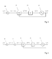
- Fig. 2 shows a dynamic clocking network 22 comprising a plurality of interconnected clocking nodes 21 that are continuously delay-coupled. Each clocking node is implemented as a PLL. Thus, the clocking network 22 is network of mutually delay-coupled PLLs with continuous coupling.
- the PLL comprises a phase detector 31, a loop filter 32 and a voltage controlled oscillator 33 that generates a time-continuous clocking signal x k ( t ) .
- the PLL synchronizes the phase of the clocking signal generated by the VCO 33 with the phase of the external clocking signal x l ( t - ⁇ s ) which is delayed by the transmission time delay ⁇ s , indicated by transmission delayer 34, by adjusting the frequency of the clocking signal of the VCO such that a network-wide synchronization of the VCOs is achieved for all clocking nodes of the dynamic clocking network.
- the phase detector 31 compares the phase of the external clocking signal x l ( t - ⁇ s ) with the phase of the clocking signal x k ( t ) generated by the VCO 33 to generate phase detector signal x k PD t . After filtering with the loop filter 32 this yields the control signal x k ( t ) for the VCO 33.
- Fig. 4 shows the node of Fig. 3 comprising an additional delayer 45 to adjust the total time delay.
- Transmission time delay ⁇ s and additional time delay ⁇ d yield the total time delay ⁇ T .
- the phase detector 41 compares the phase of the additionally delayed external clocking signal x l (t- ⁇ T ) with the phase of the clocking signal x k ( t ) generated by the VCO 43 to generate the phase detector signal x k PD t . After filtering with the loop filter 42 this yields the control signal x k ( t ) for the VCO 43.
- Fig. 5 shows a clocking node with a plurality of external clocking signals x 1 ( t ), x 2 ( t ), x 3 ( t ), .. x n ( t ) .
- Each input path comprises an individual delayer 551, 552, 553, 554 that induces an additional time delay to the transmission time delay indicated by transmission delayers 541, 542, 543, 544.
- Each phase detector 511, 512, 513, 514 compares the phase of the clocking signal x k ( t ) generated by the controllable oscillator 53 with the phase of each external clock signal individually to generate a plurality of phase detector signals.
- the combiner 56 combines the phase detector signals to generate a combined phase detector signal to control the controllable oscillator.
- the combined phase detector signal is filtered by the loop filter 52 to yield the control signal x k ( t ) for the VCO.
- the PLL of each clocking node thus adjusts the frequency of the clocking signal of each VCO such that a network-wide synchronization of the VCOs is achieved for all clocking nodes of the dynamic clocking network. By properly inducing individual additional time delays to each input path, stable solutions for the collective frequency of the network can be achieved.
- Fig. 6 shows a clocking node with a plurality of external clocking signals x 1 ( t ), x 2 ( t ), x 3 ( t ), .. x n ( t ) .
- Each input path comprises an individual delayer 651, 652, 653, 654 that induces an additional time delay to the transmission time delay indicated by transmission delayers 641, 642, 643, 644.
- the combiner 66 combines the plurality of external clocking signals to generate a combined external clocking signal.
- the phase detector 61 compares the phase of the clocking signal generated by the VCO 63 with the phase of the combined external clocking signal to generate the phase detector signal x k PD t . After filtering with the loop filter 62 this yields the control signal x k C t for the VCO 63.
- Fig. 7 shows the clocking node of Fig. 4 comprising a feedback delayer 77 for introducing a time delay in the feedback loop of the PLL comprising the phase detector 71, loop filter 72 and VCO 73.
- the feedback delay may be induced to compensate for a total time delay.
- the individual total time delays ⁇ T in any of the described embodiments are design parameters. Only if chosen properly, a stable synchronous state can be achieved as will be explained with reference to Fig. 8 which shows the global frequency ⁇ of the in-phase and anti-phase synchronized state as a function of the total time delay ⁇ T for a clocking network comprising two clocking nodes.
- Full lines denote stable solutions and dashed lines denote unstable solutions.
- the total time delay can be chosen for a given free running frequency of the VCO in order to achieve a desired synchronous state and global frequency of the network. If no additional time delay is induced, the transmission time delay corresponds to the total time delay.
- a transmission time delay can be achieved that yields a stable synchronous state.
- the total time delay may be chosen such that a perturbation response rate given by Re( ⁇ ) is minimized, see Eq. (14).
- Fig. 10 shows a diagram showing the perturbation response rate versus the total time delay for a clocking network comprising two clocking nodes.
- Fig. 11 shows the perturbation response rate versus the total time delay for different cut-off frequencies of the loop filter.
- the present invention proposes a novel synchronization strategy, specifically for spatially distributed clocks. These clocks are synchronized by networks of mutually coupled phase-locked loops. An important feature is the total time delay in the time-continuous coupling between phase-looked loops which enables synchronized states in the presence of a non-attractive coupling mechanism. As the transmission time delay is not limited to one eighth of a period of the oscillator as is the case with the solution disclosed in WO 2013/178237 A1 , networks with larger total time delays between nodes can be synchronized. Important applications are, e.g., high performance MPSoCs architectures, distributed antenna arrays, and other large scale electronic clocking systems communicating by means of time-continuous signals.
- the present invention specifically provides a simplified clock network compared to the prior art tree structure.
- the synchronized network thus enables an increased energy efficiency due to shorter connections and less amplification. Moreover, it exhibits increased robustness towards failure of individual components due to decentralized architecture. Furthermore, the synchronized network is designed for high quality of oscillations.
- the synchronized network can be realized using readily available hardware components. Thus, this solution works with readily available hardware combined in a novel way and additionally simplifies clock distribution, thereby reducing power consumption and increasing scalability.
Landscapes
- Engineering & Computer Science (AREA)
- Theoretical Computer Science (AREA)
- Physics & Mathematics (AREA)
- General Engineering & Computer Science (AREA)
- General Physics & Mathematics (AREA)
- Computer Networks & Wireless Communication (AREA)
- Signal Processing (AREA)
- Stabilization Of Oscillater, Synchronisation, Frequency Synthesizers (AREA)
- Synchronisation In Digital Transmission Systems (AREA)
Abstract
Description
- The present invention relates to a synchronizable network. The present invention specifically relates to clock distribution and self-organized synchronization in large scale networks, like high performance Multiprocessor System-on-Chips (MPSoCs) architectures.
- Enabled by sub-micrometer semiconductor device fabrication technologies MPSoCs have become a key component for modern communications and computation systems. Lately, the trend to integrate more and more processing cores in a single silicon die has gained momentum, aided by promising benefits in mechanical footprint, computational performance, energy and cost efficiency. Hence, increasing the number of cores directly translates into high performance through parallel processing and high efficiency compared to single-core solutions.
- Nowadays, hundreds of thousands of cores are integrated on one single chip. To ensure a stable and well defined system a common synchronization strategy is to separate clocking of the processing blocks. The globally asynchronous locally synchronous (GALS) clocking yields a simplified clock tree and allows clock generation on-chip to minimize the number of required I/O pins. Hence, the clock frequencies and supply voltages, within a heterogeneous MPSoC, can be dynamically adjusted per core. However, the flexibility, scalability and other benefits of GALS clocking technique goes along with performance penalties caused by additional communication latencies between disjoint clock domains. This exactly describes the bottleneck of the GALs approach.
- In contrast, for high performance microprocessors a globally synchronous design as shown in
Fig. 1 , where allcores 12 of a clocking network 11 share onemaster clock 13, is used. The communication latencies between cores are drastically reduced compared to GALS clocking. Considering next generation MPSoCs, a very large chip area has to be clocked synchronously. Implementing a master clock based clock tree, seeFig. 1 , the clock signals within MPSoCs have to be transmitted over ranges of some millimeters, which is a well-known bottleneck for speed, power and reliability. Furthermore, traditional globally synchronous clocking circuits have become too difficult for large MPSoCs with many cores, constantly growing chip size and wire induced delays. In addition, the clock trees consume a significant amount of power which is critical for mobile communication systems. - Both clocking techniques, GALS and the globally synchronous design, reach their limits at large scale networks like massive MPSoCs.
- Another strategy for network synchronization and clock distribution relates to self-organized synchronization of distributed network nodes in absence of an entraining master clock.
- "Mutually connected phase-locked loop networks: dynamical models and design parameters" by F.M. Orsatti, R. Carareto, J.R.C. Piqueira, IET Circuit Devices Syst.,2008, Vol. 2, No. 6, pp. 495-508 relates to distributing clock signals by using mutually connected architectures instead of master-slave type architectures. Mutually connected digital PLL networks are studied and conditions for the existence of synchronized states are derived, depending on individual node parameters and network connectivity, considering that the nodes are nonlinear oscillators with nonlinear coupling conditions.
- "Multiple synchronous states in static delay-free mutually connected PLL networks" by F.M. Orsatti, R. Carareto, J.R.C. Piqueira, Signal Processing 90 (2010) 2072-2082 relates to mutually connected networks of digital phase-locked loops. Even for static networks without delays, different synchronous states may exist for the network.
- However, these papers deal with networks for which a time delay between oscillators is not present or negligible. Hence, the solution presented there cannot be applied to networks exhibiting a significant time delay between network nodes.
-
WO 2013/178237 A1 relates to a communication network of interconnected communication nodes, each node comprising an oscillator that is mutually coupled to oscillators of other communication nodes. The oscillator generates periodic synchronization pulses. The communication node further comprises a transmitter for transmitting the synchronization pulses to other communication nodes; a receiver for receiving synchronization pulses from other communication nodes; and a synchronization unit for synchronizing the phase of the synchronization pulses generated by the oscillator with the phase of the synchronization pulses received from other communication nodes by adjusting the phase of the synchronization pulses generated by the oscillator upon receipt of synchronization pulses from other communication nodes. The synchronization unit adjusts the phase of the synchronization pulses generated by the oscillator in such a way that a guaranteed network-wide synchronization is achieved for all communication nodes of the communication network. However,WO 2013/178237 A1 explicitly limits a transmission time delay of the synchronization pulses between the communication nodes to one eighth of the period of the oscillator. Hence, this disclosure does not provide a suitable solution for networks exhibiting a transmission time delay exceeding one eighth of the period of the oscillator, e.g., highly integrated chip networks. Moreover, this solution assumes pulse coupling. Stochastic synchronization pulse emission is required to guarantee synchronization. Hence, this solution is not suitable for clock distributions with time-continuous coupling. - It is an objective of the present invention to provide a solution for synchronizing a network comprising a plurality of interconnected nodes that provides a stable synchronized state, especially for large scale networks.
- This objective is achieved with a node according to the independent apparatus claim and a method for synchronizing a network according to the independent method claim.
- The present invention relates to a node for a network comprising a plurality of interconnected nodes. The node comprises a controllable oscillator generating a time-continuous synchronization signal for synchronizing the plurality of interconnected nodes of the network. The node further comprises a controller for comparing and synchronizing a phase of the time-continuous synchronization signal generated by the controllable oscillator, which is transmitted to another node of the network, with the phase of an external time-continuous synchronization signal received from the other node of the network by adjusting a frequency of the time-continuous synchronization signal generated by the controllable oscillator. The external time-continuous synchronization signal received from the other node of the network is delayed with respect to the time-continuous synchronization signal transmitted by the other node by a total time delay. The total time delay may be a transmission time delay resulting from a transmission time between the transmission of the external time-continuous synchronization signal by the other node and the following receipt of the external time-continuous synchronization signal by the node. The total time delay may also comprise any tunable additional time delays in addition to the transmission time delay. The controller iteratively adjusts the frequency of the time-continuous synchronization signal generated by the controllable oscillator such that a network-wide synchronization of oscillators is achieved for all nodes of the network. The synchronization is thus achieved in a continuous self-organized process in interaction with the other node of the network.
- The controller may be any control system with feedback of the continuous synchronization signal generated by the tunable oscillator.
- Specifically, the controller in combination with the controllable oscillator may form a phase locked loop (PLL). PLLs are electronic components able to synchronize their synchronization signals by evaluating mutual phase differences and adjusting their frequencies accordingly. The controller then comprises a phase detector (PD) and a loop filter (LF). The controllable oscillator may be a voltage controlled oscillator (VCO). The phase detector compares the phase of the external time-continuous synchronization signal with the phase of the time-continuous synchronization signal generated by the controllable oscillator.
- A model for mutually coupled PLLs is described below using an analog PLL as an example. The present invention is not restricted to analog PLLs.
- The VCOs output a sinusoidal with constant amplitude, which can be set to 1 without loss of generality,


- This signal



- Eq. (5) can be extended to a phase model for N delay coupled PLLs with transmission delays between coupled oscillators. A standard state-of-the-art PLL handles only a single input signal. The controller then compares and synchronizes a phase of the time-continuous synchronization signal generated by the controllable oscillator with the phases of external time-continuous synchronization signals received from a plurality of other nodes of the network by adjusting a frequency of the time-continuous synchronization signal generated by the controllable oscillator.
- One aspect of the present invention relates to a combiner for combining external time-continuous synchronization signals received from other nodes of the network to generate a combined external time-continuous synchronization signal. The phase detector compares the phase of the time-continuous synchronization signal generated by the controllable oscillator with the phase of the combined external time-continuous synchronization signal. The combiner may be part of the phase detector (PD). The combiner may be a non-inverting adder. The phase detector (PD) may be a multiplier for analog signals or an XOR gate for digital signals. Alternatively, the phase detector may compare the phase of the time-continuous synchronization signal generated by the controllable oscillator with the phase of each external time-continuous synchronization signal individually to generate a plurality of phase detector signals. The combiner then combines the phase detector signals to control the controllable oscillator.
- The phase model for N coupled analog PLLs reads

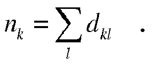
- The connections between PLLs are described by the coupling matrix D=(dkl ) with dkl ∈{0,1}, where dkl =1 indicates a connection between k and l. The coupling strength is normalized by the number of input signals

- In global in-phase synchronous states, the phase of all oscillators satisfy


- One aspect of the present invention relates to tuning the total time delay between mutually coupled PLLs. A stable in-phase synchronized solution, Eq. (8), with global frequency Ω cannot be achieved for arbitrary total time delays between coupled synchronizers. The total time delay is a design parameter and can be tuned by an additional delayer and the design of the network. A node may comprise a delayer for inducing an additional time delay to a transmission time delay. The total time delay effectively induces a frequency-dependent phase shift to a synchronization signal and, if appropriately tuned, changes the coupling properties such that stable synchronized states become possible. A delayer may be any means suitable to induce such phase shifts. The delayer may need to be specifically tuned for each input path.
- The total time delay may comprise a period of the controllable oscillator. Specifically, it may exceed one eighth of a period of the controllable oscillator. Thus, networks with large delays can be synchronized.
- The node may further comprise a feedback delayer for inducing a feedback delay τf in a feedback path between the controllable oscillator and the phase detector. The feedback delay may compensate for the total time delay. The collective frequency then depends on the difference between the total time delay and the feedback delay.
- Furthermore, the total time delay may be tuned such that it minimizes a perturbation response rate λ in order to arrive at an in-phase synchronized state with maximum stability as will be explained.
- For a phase perturbed by a perturbation qk (t)


- Substituting the exponential ansatz qk (t)=ckeλt, where λ is complex, into Eq. (11) the characteristic equation is given by


- Solutions for λ can be obtained by rewriting Eq. (13) in vector form


- For an arbitrary 2π-periodic coupling function h, the term α in Eq. (14) satisfies:


- Thus, for a desired collective frequency Ω the total time delay τT in combination with the feedback delay τf may be tuned such that a maximum perturbation decay can be achieved by optimizing the perturbation response rate λ, see Eq. (9).
- Moreover, further design parameters for optimizing the perturbation response rate λ are the free running frequency ω of the controllable oscillator, the coupling strength K, and the impulse response p(u) of a filter within the controller, i.e., the loop filter.
- One aspect of the present invention relates to optimizing the perturbation response by tuning the cut-off frequency of the loop filter.
- A large class of loop filters can be described by an impulse response p(t) given by the Gamma distribution,


- Substituting into Eq. (14), the characteristic equation is given by:

- This equation can have multiple solutions in λ for each eigenvalue ζ.
- The time-continuous synchronization signal may be a digital signal or an analog signal. The node may be a clocking node and the time-continuous synchronization signal may be a clock signal for clocking the clocking node.
- The present invention further relates to a network comprising a plurality of interconnected nodes that are continuously coupled. The network may be designed to yield a desired perturbation response rate and/or collective frequency. A design parameter of the network is the distance between a node and another node that determines the total time delay. The total time delay corresponding to an optimum perturbation response rate may be achieved either by adjusting the distance alone and/or the additional time delay induced by a delayer.
- The present invention further relates to a method for synchronizing a network comprising a plurality of interconnected nodes. The method comprises generating a time-continuous synchronization signal in each node; transmitting the time-continuous synchronization signal of each node to at least one other respective node of the network; receiving in each node a delayed external time-continuous synchronization signal from the at least one respective other node of the network; and synchronizing in each node a phase of the time-continuous synchronization signal with a phase of the external time-continuous synchronization signal received from the at least one other node by iteratively adjusting the frequency of the time-continuous synchronization signal such that a network-wide synchronization is achieved for all nodes of the network in a continuous self-organized process.
- Node, network and related method according to the invention are described in more detail herein below by way of exemplary embodiments and with reference to the attached drawings, in which:
- Fig. 1
- shows a prior art approach for clock distribution on a globally synchronous network involving a master clock;
- Fig. 2
- shows an approach of a dynamic clocking network involving mutually coupled nodes, which are able to globally synchronize in a self-organized manner;
- Fig. 3
- shows a block diagram of a network node comprising a delay-coupled PLL according to a first embodiment;
- Fig. 4
- shows a block diagram of a network node comprising a delay-coupled PLL and an additional delayer according to a second embodiment;
- Fig. 5
- shows a block diagram of a network node comprising a delay-coupled PLL, an additional delayer for each input and a combiner to combine a plurality of phase detector signals according to a third embodiment;
- Fig. 6
- shows a block diagram of a network node comprising a delay-coupled PLL, an additional delayer for each input and a combiner to combine a plurality of input signals according to a fourth embodiment;
- Fig. 7
- shows a block diagram of a network node comprising a delay-coupled PLL and a feedback delayer according to a fifth embodiment;
- Fig. 8
- shows a diagram showing a global frequency of the in-phase and anti-phase synchronized state versus the transmission delay; and
- Fig. 9
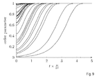
- shows a diagram showing global synchrony measured using the Kuramoto order parameter as a function of time;
- Fig. 10
- shows a diagram showing the perturbation response rate versus the transmission delay; and
- Fig. 11
- shows a diagram showing the perturbation response rate versus the transmission delay for different cut-off frequencies of the loop filter.
-
Fig. 2 shows adynamic clocking network 22 comprising a plurality ofinterconnected clocking nodes 21 that are continuously delay-coupled. Each clocking node is implemented as a PLL. Thus, theclocking network 22 is network of mutually delay-coupled PLLs with continuous coupling. - Referring to
Fig. 3 , the PLL comprises aphase detector 31, aloop filter 32 and a voltage controlledoscillator 33 that generates a time-continuous clocking signal xk (t). The PLL synchronizes the phase of the clocking signal generated by theVCO 33 with the phase of the external clocking signal xl (t-τs ) which is delayed by the transmission time delay τs , indicated bytransmission delayer 34, by adjusting the frequency of the clocking signal of the VCO such that a network-wide synchronization of the VCOs is achieved for all clocking nodes of the dynamic clocking network. To do so, thephase detector 31 compares the phase of the external clocking signal xl (t-τs ) with the phase of the clocking signal xk (t) generated by theVCO 33 to generate phase detector signal
loop filter 32 this yields the control signal xk (t) for theVCO 33. -
Fig. 4 shows the node ofFig. 3 comprising anadditional delayer 45 to adjust the total time delay. Transmission time delay τs and additional time delay τd yield the total time delay τT . Thephase detector 41 compares the phase of the additionally delayed external clocking signal xl (t-τT ) with the phase of the clocking signal xk (t) generated by theVCO 43 to generate the phase detector signal
loop filter 42 this yields the control signal xk (t) for theVCO 43. By properly inducing an additional time delay, stable solutions for the collective frequency of the network can be achieved. -
Fig. 5 shows a clocking node with a plurality of external clocking signals x 1(t), x 2(t), x 3(t), .. xn (t). Each input path comprises anindividual delayer transmission delayers phase detector controllable oscillator 53 with the phase of each external clock signal individually to generate a plurality of phase detector signals. Thecombiner 56 combines the phase detector signals to generate a combined phase detector signal to control the controllable oscillator. The combined phase detector signal is filtered by theloop filter 52 to yield the control signal xk (t) for the VCO. The PLL of each clocking node thus adjusts the frequency of the clocking signal of each VCO such that a network-wide synchronization of the VCOs is achieved for all clocking nodes of the dynamic clocking network. By properly inducing individual additional time delays to each input path, stable solutions for the collective frequency of the network can be achieved. -
Fig. 6 shows a clocking node with a plurality of external clocking signals x 1(t), x 2(t), x 3(t), .. xn (t). Each input path comprises anindividual delayer transmission delayers Fig. 5 , where a combiner combines a plurality of phase detector signals, in this embodiment thecombiner 66 combines the plurality of external clocking signals to generate a combined external clocking signal. Thephase detector 61 compares the phase of the clocking signal generated by theVCO 63 with the phase of the combined external clocking signal to generate the phase detector signal
loop filter 62 this yields the control signal
VCO 63. -
Fig. 7 shows the clocking node ofFig. 4 comprising afeedback delayer 77 for introducing a time delay in the feedback loop of the PLL comprising thephase detector 71,loop filter 72 andVCO 73. The feedback delay may be induced to compensate for a total time delay. - The individual total time delays τT in any of the described embodiments are design parameters. Only if chosen properly, a stable synchronous state can be achieved as will be explained with reference to
Fig. 8 which shows the global frequency Ω of the in-phase and anti-phase synchronized state as a function of the total time delay τT for a clocking network comprising two clocking nodes. The anti-phase synchronized state is characterized by φ 1(t)=φ 2(t)-π. Full lines denote stable solutions and dashed lines denote unstable solutions. Hence, for a desired global frequency of the clocking network, the total time delay can be chosen for a given free running frequency of the VCO in order to achieve a desired synchronous state and global frequency of the network. If no additional time delay is induced, the transmission time delay corresponds to the total time delay. Thus, by choosing the distances between the coupled nodes of the network accordingly, a transmission time delay can be achieved that yields a stable synchronous state. - The curves of
Fig. 8 are shown for the following system parameters: VCO free running frequency ω = 2n × 3.55 GHz, coupling strength K = 2n × 1.11 GHz, LF order a = 1, LF cut-off frequency ωc = 2n × 355 MHz. The frequencies of the different solutions can be obtained by letting the clocking network evolve from different initial phase differences. For example, for τT =0.2·2π/ω, all initial phase differences lead to the in-phase synchronized state, seeFig. 8 , wherein an order parameter of zero means no synchrony and wherein a value of one implies full synchrony. For values of the total time delay for which both solutions are stable, the clock network evolves towards one solution according to its initial condition. - Moreover, the total time delay may be chosen such that a perturbation response rate given by Re(λ) is minimized, see Eq. (14).
-
Fig. 10 shows a diagram showing the perturbation response rate versus the total time delay for a clocking network comprising two clocking nodes. The coupling matrix corresponding to two mutually coupled PLLs is given by
Fig. 8 , up or down. - The coupling strength and the cut-off frequency of the loop filter also affects the stability of the clock network.
Fig. 11 shows the perturbation response rate versus the total time delay for different cut-off frequencies of the loop filter. - Thus, by properly tuning the total time delay in combination with the cut-off frequency a minimum perturbation response rate can be achieved.
- The present invention proposes a novel synchronization strategy, specifically for spatially distributed clocks. These clocks are synchronized by networks of mutually coupled phase-locked loops. An important feature is the total time delay in the time-continuous coupling between phase-looked loops which enables synchronized states in the presence of a non-attractive coupling mechanism. As the transmission time delay is not limited to one eighth of a period of the oscillator as is the case with the solution disclosed in
WO 2013/178237 A1 , networks with larger total time delays between nodes can be synchronized. Important applications are, e.g., high performance MPSoCs architectures, distributed antenna arrays, and other large scale electronic clocking systems communicating by means of time-continuous signals. - The present invention specifically provides a simplified clock network compared to the prior art tree structure. The synchronized network thus enables an increased energy efficiency due to shorter connections and less amplification. Moreover, it exhibits increased robustness towards failure of individual components due to decentralized architecture. Furthermore, the synchronized network is designed for high quality of oscillations. The synchronized network can be realized using readily available hardware components. Thus, this solution works with readily available hardware combined in a novel way and additionally simplifies clock distribution, thereby reducing power consumption and increasing scalability.
Claims (15)
- Node (21) for a network (22) comprising a plurality of interconnected nodes, each node (21) comprising:a controllable oscillator (33) generating a time-continuous synchronization signal for synchronizing the plurality of interconnected nodes of the network;a controller (31, 32) for comparing and synchronizing a phase of the time-continuous synchronization signal generated by the controllable oscillator (33), which is transmitted to another node of the network, with the phase of an external time-continuous synchronization signal received from the other node of the network by adjusting a frequency of the time-continuous synchronization signal generated by the controllable oscillator,wherein the external time-continuous synchronization signal received from the other node of the network is delayed with respect to the external time-continuous synchronization signal transmitted by the other node by a total time delay; andwherein the controller (33) iteratively adjusts the frequency of the time-continuous synchronization signal generated by the controllable oscillator such that a network-wide synchronization of oscillators is achieved for all nodes of the network in a continuous self-organized process in interaction with the other node of the network.
- The node according to claim 1, wherein the controller comprises a phase detector (31) configured to compare the phase of the external time-continuous synchronization signal with the phase of the time-continuous synchronization signal generated by the controllable oscillator.
- The node according to claim 1 or 2, wherein the controller (61, 62) compares and synchronizes a phase of the time-continuous synchronization signal generated by the controllable oscillator (63), which is transmitted to other nodes of the network, with the phases of external time-continuous synchronization signals received from other nodes of the network by adjusting a frequency of the time-continuous synchronization signal generated by the controllable oscillator,
wherein the external time-continuous synchronization signals received from other nodes of the network are delayed with respect to the time-continuous synchronization signal transmitted by the other nodes by a total time delay; and
wherein the controller (61, 62) iteratively adjusts the frequency of the time-continuous synchronization signal generated by the controllable oscillator such that a network-wide synchronization of oscillators is achieved for all nodes of the network in a continuous self-organized process in interaction with the other nodes of the network. - The node according to claim 3, further comprising a combiner (66) to combine the external time-continuous synchronization signals received from other nodes of the network to generate a combined external time-continuous synchronization signal and wherein the phase detector compares (61) the phase of the time-continuous synchronization signal generated by the controllable oscillator (63) with the phase of the combined external time-continuous synchronization signal.
- The node according to claim 3, wherein the phase detector (511, 512, 513, 514) compares the phase of the time-continuous synchronization signal generated by the controllable oscillator with the phase of each external time-continuous synchronization signal individually to generate a plurality of phase detector signals; and wherein the combiner (56) combines the phase detector signals to control the controllable oscillator (53).
- The node according to claim 4 or 5, wherein the controller comprises the combiner (56; 66).
- The node according to any of claims 1 to 6 comprising a delayer (45) for inducing an additional time delay in addition to a transmission time delay to yield the total time delay.
- The node according to any of claims 3 to 6 comprising a plurality of delayers (551, 552, 553, 554; 651, 652, 653, 654) for inducing an additional time delay in addition to a transmission time delay to yield the total time delay for each received external time-continuous synchronization signal.
- The node according to any of claims 1 to 8 comprising a feedback delayer (77) for inducing a feedback time delay in a feedback path between the controllable oscillator (73) and the phase detector (71).
- The node according to any of claims 1 to 9, wherein at least one of the following parameters: the total time delay τT , the feedback delay τf , a free running frequency ω of the controllable oscillator, a coupling strength K , an impulse response p(u) of a filter within the controller, is tuned to yield a desired perturbation response rate λ and/or collective frequency Ω.
- The node according to claim 10, wherein the desired perturbation response rate λ solves

α=Kh'(-Ω[τT -τf ]), wherein h' denotes a first derivative of a coupling function h;

wherein the collective frequency Ω solves:
- Node according to any of claims 1 to 11, wherein the time-continuous synchronization signal is a digital signal or an analog signal.
- Node according to any of claims 1 to 12, wherein the node (21) is a clocking node and wherein the time-continuous synchronization signal is a clock signal for clocking the clocking node.
- Network (22) comprising a plurality of interconnected nodes (21) according to any of claims 1 to 13 that are time-continuously coupled comprising a distance between a node and another node determining total time delays to yield a desired perturbation response rate and/or collective frequency.
- Method for synchronizing a network comprising a plurality of interconnected nodes, the method comprising:generating a time-continuous synchronization signal in each node;transmitting the time-continuous synchronization signal of each node to at least one other respective node of the network;receiving in each node a delayed external time-continuous synchronization signal from the at least one respective other node of the network; andsynchronizing in each node a phase of the time-continuous synchronization signal with a phase of the external time-continuous synchronization signal received from the at least one respective other node by iteratively adjusting the frequency of the time-continuous synchronization signal such that a network-wide synchronization is achieved for all nodes of the network in a continuous self-organized process.
Priority Applications (6)
| Application Number | Priority Date | Filing Date | Title |
|---|---|---|---|
| EP14173279.2A EP2957982B1 (en) | 2014-06-20 | 2014-06-20 | Self-synchronizable network |
| PCT/EP2015/064008 WO2015193512A1 (en) | 2014-06-20 | 2015-06-22 | Self-synchronizable network |
| TW104120060A TWI721948B (en) | 2014-06-20 | 2015-06-22 | Synchronizable network and method for synchronizing network |
| KR1020177001616A KR102029320B1 (en) | 2014-06-20 | 2015-06-22 | Self-synchronizable network |
| US15/316,307 US10241539B2 (en) | 2014-06-20 | 2015-06-22 | Self-synchronizable network |
| CN201580032941.6A CN106462177B (en) | 2014-06-20 | 2015-06-22 | Self-synchronizable network |
Applications Claiming Priority (1)
| Application Number | Priority Date | Filing Date | Title |
|---|---|---|---|
| EP14173279.2A EP2957982B1 (en) | 2014-06-20 | 2014-06-20 | Self-synchronizable network |
Publications (2)
| Publication Number | Publication Date |
|---|---|
| EP2957982A1 true EP2957982A1 (en) | 2015-12-23 |
| EP2957982B1 EP2957982B1 (en) | 2017-08-09 |
Family
ID=51062668
Family Applications (1)
| Application Number | Title | Priority Date | Filing Date |
|---|---|---|---|
| EP14173279.2A Not-in-force EP2957982B1 (en) | 2014-06-20 | 2014-06-20 | Self-synchronizable network |
Country Status (6)
| Country | Link |
|---|---|
| US (1) | US10241539B2 (en) |
| EP (1) | EP2957982B1 (en) |
| KR (1) | KR102029320B1 (en) |
| CN (1) | CN106462177B (en) |
| TW (1) | TWI721948B (en) |
| WO (1) | WO2015193512A1 (en) |
Cited By (1)
| Publication number | Priority date | Publication date | Assignee | Title |
|---|---|---|---|---|
| CN105743555A (en) * | 2016-03-25 | 2016-07-06 | 四川大学 | Split-ranging type distributed antenna transmitted beam optimized formation method |
Families Citing this family (2)
| Publication number | Priority date | Publication date | Assignee | Title |
|---|---|---|---|---|
| DE102017127805B4 (en) * | 2017-11-24 | 2019-10-17 | Infineon Technologies Ag | Oscillator arrangement and method for synchronizing an oscillator |
| CN109829536A (en) * | 2019-02-20 | 2019-05-31 | 杭州职业技术学院 | A Genetic Algorithm-Based Optimization Method for Network Synchronization Performance |
Citations (2)
| Publication number | Priority date | Publication date | Assignee | Title |
|---|---|---|---|---|
| US20090183019A1 (en) * | 2008-01-14 | 2009-07-16 | Allen David H | Power Supply Current Spike Reduction Techniques for an Integrated Circuit |
| WO2013178237A1 (en) | 2012-05-31 | 2013-12-05 | Max-Planck-Gesellschaft zur Förderung der Wissenschaften e. V. | Communication node and method for self-organizing synchronization of a communication network |
Family Cites Families (6)
| Publication number | Priority date | Publication date | Assignee | Title |
|---|---|---|---|---|
| GB2279190A (en) * | 1993-06-15 | 1994-12-21 | Ibm | Synchronisation apparatus |
| US7218229B2 (en) | 2003-11-07 | 2007-05-15 | Wherenet Corp | Location system and method that achieves time synchronized network performance with nodes divided into separate networks |
| KR100574980B1 (en) * | 2004-04-26 | 2006-05-02 | 삼성전자주식회사 | Phase-locked loop for fast frequency lock |
| KR100594297B1 (en) * | 2004-10-12 | 2006-06-30 | 삼성전자주식회사 | Delay Synchronous Loop and Method Using Oscillator Adapting to Frequency of External Clock Signal |
| CN102237941B (en) * | 2010-04-28 | 2015-06-03 | 中兴通讯股份有限公司 | Time synchronization system and method |
| US9209959B2 (en) * | 2012-03-26 | 2015-12-08 | Electronics And Telecommunications Research Institute | Method of frequency synchronization in distributed network |
-
2014
- 2014-06-20 EP EP14173279.2A patent/EP2957982B1/en not_active Not-in-force
-
2015
- 2015-06-22 TW TW104120060A patent/TWI721948B/en not_active IP Right Cessation
- 2015-06-22 KR KR1020177001616A patent/KR102029320B1/en not_active Expired - Fee Related
- 2015-06-22 US US15/316,307 patent/US10241539B2/en active Active
- 2015-06-22 WO PCT/EP2015/064008 patent/WO2015193512A1/en not_active Ceased
- 2015-06-22 CN CN201580032941.6A patent/CN106462177B/en not_active Expired - Fee Related
Patent Citations (2)
| Publication number | Priority date | Publication date | Assignee | Title |
|---|---|---|---|---|
| US20090183019A1 (en) * | 2008-01-14 | 2009-07-16 | Allen David H | Power Supply Current Spike Reduction Techniques for an Integrated Circuit |
| WO2013178237A1 (en) | 2012-05-31 | 2013-12-05 | Max-Planck-Gesellschaft zur Förderung der Wissenschaften e. V. | Communication node and method for self-organizing synchronization of a communication network |
Non-Patent Citations (3)
| Title |
|---|
| F.M. ORSATTI; R. CARARETO; J.R.C. PIQUEIRA: "Multiple synchronous states in static delay-free mutually connected PLL networks", SIGNAL PROCESSING, vol. 90, 2010, pages 2072 - 2082 |
| F.M. ORSATTI; R. CARARETO; J.R.C. PIQUEIRA: "Mutually connected phase-locked loop networks: dynamical models and design parameters", IET CIRCUIT DEVICES SYST., vol. 2, no. 6, 2008, pages 495 - 508 |
| F.M. ORSATTI; R. CARARETO; J.R.C. PIQUEIRA: "Mutually connected phase-locked loop networks: dynamical models and design parameters", IET CIRCUIT DEVICES SYST., vol. 2, no. 6, 2008, pages 495 - 508, XP002733443 * |
Cited By (2)
| Publication number | Priority date | Publication date | Assignee | Title |
|---|---|---|---|---|
| CN105743555A (en) * | 2016-03-25 | 2016-07-06 | 四川大学 | Split-ranging type distributed antenna transmitted beam optimized formation method |
| CN105743555B (en) * | 2016-03-25 | 2018-08-14 | 四川大学 | One kind divides formula distribution antenna launching beam to optimize forming method |
Also Published As
| Publication number | Publication date |
|---|---|
| CN106462177B (en) | 2020-02-07 |
| CN106462177A (en) | 2017-02-22 |
| KR102029320B1 (en) | 2019-11-08 |
| US20170139438A1 (en) | 2017-05-18 |
| TW201601566A (en) | 2016-01-01 |
| US10241539B2 (en) | 2019-03-26 |
| KR20170021303A (en) | 2017-02-27 |
| WO2015193512A1 (en) | 2015-12-23 |
| TWI721948B (en) | 2021-03-21 |
| EP2957982B1 (en) | 2017-08-09 |
Similar Documents
| Publication | Publication Date | Title |
|---|---|---|
| US5481573A (en) | Synchronous clock distribution system | |
| CN103957003B (en) | A kind of time-to-digit converter, frequency tracking apparatus and method | |
| KR100963859B1 (en) | Clock generator | |
| EP3076553B1 (en) | Clock synchronizer | |
| EP2404379B1 (en) | Crystal-based oscillator for use in synchronized system | |
| US10523224B2 (en) | Techniques for signal skew compensation | |
| CN104821802B (en) | Clock generation method and clock forming circuit | |
| JP6485003B2 (en) | Signal generation system and method | |
| EP2957982B1 (en) | Self-synchronizable network | |
| US20190011945A1 (en) | Method and apparatus to utilize a digital-time-conversion (dtc) based clocking in computing systems | |
| CN102823137A (en) | Apparatus and method to compensate for injection locking | |
| CN103684440B (en) | Clock and data recovery circuit and clock and data recovery method | |
| US20130088268A1 (en) | Multi-Phase Clock Generation System and Clock Calibration Method Thereof | |
| US7501865B1 (en) | Methods and systems for a digital frequency locked loop for multi-frequency clocking of a multi-core processor | |
| US8692595B1 (en) | Transceiver circuitry with multiple phase-locked loops | |
| US9806701B1 (en) | Digital frequency multiplier to generate a local oscillator signal in FDSOI technology | |
| Kinali et al. | Fault-tolerant clock synchronization with high precision | |
| CN111446957A (en) | Multi-P LL parallel output clock synchronization system and working method thereof | |
| US8373476B2 (en) | Device and method for compensating a signal propagation delay | |
| Piqueira et al. | Double-frequency jitter in chain master-slave clock distribution networks: comparing topologies | |
| CN101436856A (en) | Frequency synchronization device, frequency synchronization method and frequency generation device using the same | |
| US6636532B1 (en) | Apparatus for adjusting phase | |
| US6489852B1 (en) | Slew controlled frame aligner for a phase locked loop | |
| EP2992636B1 (en) | Synchronous data system and method for providing phase-aligned output data | |
| CN109787620A (en) | A kind of method and device of the calibration frequency based on digital frequency divider |
Legal Events
| Date | Code | Title | Description |
|---|---|---|---|
| PUAI | Public reference made under article 153(3) epc to a published international application that has entered the european phase |
Free format text: ORIGINAL CODE: 0009012 |
|
| AK | Designated contracting states |
Kind code of ref document: A1 Designated state(s): AL AT BE BG CH CY CZ DE DK EE ES FI FR GB GR HR HU IE IS IT LI LT LU LV MC MK MT NL NO PL PT RO RS SE SI SK SM TR |
|
| AX | Request for extension of the european patent |
Extension state: BA ME |
|
| 17P | Request for examination filed |
Effective date: 20160623 |
|
| RBV | Designated contracting states (corrected) |
Designated state(s): AL AT BE BG CH CY CZ DE DK EE ES FI FR GB GR HR HU IE IS IT LI LT LU LV MC MK MT NL NO PL PT RO RS SE SI SK SM TR |
|
| GRAP | Despatch of communication of intention to grant a patent |
Free format text: ORIGINAL CODE: EPIDOSNIGR1 |
|
| INTG | Intention to grant announced |
Effective date: 20170208 |
|
| RIN1 | Information on inventor provided before grant (corrected) |
Inventor name: WETZEL, LUCAS Inventor name: JOERG, DAVID JOSEF Inventor name: POLLAKIS, ALEXANDROS Inventor name: RAVE, WOLFGANG Inventor name: FETTWEIS, GERHARD Inventor name: JUELICHER, FRANK |
|
| GRAS | Grant fee paid |
Free format text: ORIGINAL CODE: EPIDOSNIGR3 |
|
| GRAA | (expected) grant |
Free format text: ORIGINAL CODE: 0009210 |
|
| AK | Designated contracting states |
Kind code of ref document: B1 Designated state(s): AL AT BE BG CH CY CZ DE DK EE ES FI FR GB GR HR HU IE IS IT LI LT LU LV MC MK MT NL NO PL PT RO RS SE SI SK SM TR |
|
| REG | Reference to a national code |
Ref country code: GB Ref legal event code: FG4D |
|
| REG | Reference to a national code |
Ref country code: CH Ref legal event code: EP Ref country code: AT Ref legal event code: REF Ref document number: 917505 Country of ref document: AT Kind code of ref document: T Effective date: 20170815 |
|
| REG | Reference to a national code |
Ref country code: IE Ref legal event code: FG4D |
|
| REG | Reference to a national code |
Ref country code: DE Ref legal event code: R096 Ref document number: 602014012768 Country of ref document: DE |
|
| REG | Reference to a national code |
Ref country code: NL Ref legal event code: MP Effective date: 20170809 |
|
| REG | Reference to a national code |
Ref country code: LT Ref legal event code: MG4D |
|
| REG | Reference to a national code |
Ref country code: AT Ref legal event code: MK05 Ref document number: 917505 Country of ref document: AT Kind code of ref document: T Effective date: 20170809 |
|
| PG25 | Lapsed in a contracting state [announced via postgrant information from national office to epo] |
Ref country code: LT Free format text: LAPSE BECAUSE OF FAILURE TO SUBMIT A TRANSLATION OF THE DESCRIPTION OR TO PAY THE FEE WITHIN THE PRESCRIBED TIME-LIMIT Effective date: 20170809 Ref country code: HR Free format text: LAPSE BECAUSE OF FAILURE TO SUBMIT A TRANSLATION OF THE DESCRIPTION OR TO PAY THE FEE WITHIN THE PRESCRIBED TIME-LIMIT Effective date: 20170809 Ref country code: AT Free format text: LAPSE BECAUSE OF FAILURE TO SUBMIT A TRANSLATION OF THE DESCRIPTION OR TO PAY THE FEE WITHIN THE PRESCRIBED TIME-LIMIT Effective date: 20170809 Ref country code: FI Free format text: LAPSE BECAUSE OF FAILURE TO SUBMIT A TRANSLATION OF THE DESCRIPTION OR TO PAY THE FEE WITHIN THE PRESCRIBED TIME-LIMIT Effective date: 20170809 Ref country code: SE Free format text: LAPSE BECAUSE OF FAILURE TO SUBMIT A TRANSLATION OF THE DESCRIPTION OR TO PAY THE FEE WITHIN THE PRESCRIBED TIME-LIMIT Effective date: 20170809 Ref country code: NO Free format text: LAPSE BECAUSE OF FAILURE TO SUBMIT A TRANSLATION OF THE DESCRIPTION OR TO PAY THE FEE WITHIN THE PRESCRIBED TIME-LIMIT Effective date: 20171109 Ref country code: NL Free format text: LAPSE BECAUSE OF FAILURE TO SUBMIT A TRANSLATION OF THE DESCRIPTION OR TO PAY THE FEE WITHIN THE PRESCRIBED TIME-LIMIT Effective date: 20170809 |
|
| PG25 | Lapsed in a contracting state [announced via postgrant information from national office to epo] |
Ref country code: GR Free format text: LAPSE BECAUSE OF FAILURE TO SUBMIT A TRANSLATION OF THE DESCRIPTION OR TO PAY THE FEE WITHIN THE PRESCRIBED TIME-LIMIT Effective date: 20171110 Ref country code: BG Free format text: LAPSE BECAUSE OF FAILURE TO SUBMIT A TRANSLATION OF THE DESCRIPTION OR TO PAY THE FEE WITHIN THE PRESCRIBED TIME-LIMIT Effective date: 20171109 Ref country code: IS Free format text: LAPSE BECAUSE OF FAILURE TO SUBMIT A TRANSLATION OF THE DESCRIPTION OR TO PAY THE FEE WITHIN THE PRESCRIBED TIME-LIMIT Effective date: 20171209 Ref country code: RS Free format text: LAPSE BECAUSE OF FAILURE TO SUBMIT A TRANSLATION OF THE DESCRIPTION OR TO PAY THE FEE WITHIN THE PRESCRIBED TIME-LIMIT Effective date: 20170809 Ref country code: ES Free format text: LAPSE BECAUSE OF FAILURE TO SUBMIT A TRANSLATION OF THE DESCRIPTION OR TO PAY THE FEE WITHIN THE PRESCRIBED TIME-LIMIT Effective date: 20170809 Ref country code: LV Free format text: LAPSE BECAUSE OF FAILURE TO SUBMIT A TRANSLATION OF THE DESCRIPTION OR TO PAY THE FEE WITHIN THE PRESCRIBED TIME-LIMIT Effective date: 20170809 Ref country code: PL Free format text: LAPSE BECAUSE OF FAILURE TO SUBMIT A TRANSLATION OF THE DESCRIPTION OR TO PAY THE FEE WITHIN THE PRESCRIBED TIME-LIMIT Effective date: 20170809 |
|
| PG25 | Lapsed in a contracting state [announced via postgrant information from national office to epo] |
Ref country code: RO Free format text: LAPSE BECAUSE OF FAILURE TO SUBMIT A TRANSLATION OF THE DESCRIPTION OR TO PAY THE FEE WITHIN THE PRESCRIBED TIME-LIMIT Effective date: 20170809 Ref country code: DK Free format text: LAPSE BECAUSE OF FAILURE TO SUBMIT A TRANSLATION OF THE DESCRIPTION OR TO PAY THE FEE WITHIN THE PRESCRIBED TIME-LIMIT Effective date: 20170809 Ref country code: CZ Free format text: LAPSE BECAUSE OF FAILURE TO SUBMIT A TRANSLATION OF THE DESCRIPTION OR TO PAY THE FEE WITHIN THE PRESCRIBED TIME-LIMIT Effective date: 20170809 |
|
| REG | Reference to a national code |
Ref country code: DE Ref legal event code: R097 Ref document number: 602014012768 Country of ref document: DE |
|
| PG25 | Lapsed in a contracting state [announced via postgrant information from national office to epo] |
Ref country code: SM Free format text: LAPSE BECAUSE OF FAILURE TO SUBMIT A TRANSLATION OF THE DESCRIPTION OR TO PAY THE FEE WITHIN THE PRESCRIBED TIME-LIMIT Effective date: 20170809 Ref country code: IT Free format text: LAPSE BECAUSE OF FAILURE TO SUBMIT A TRANSLATION OF THE DESCRIPTION OR TO PAY THE FEE WITHIN THE PRESCRIBED TIME-LIMIT Effective date: 20170809 Ref country code: SK Free format text: LAPSE BECAUSE OF FAILURE TO SUBMIT A TRANSLATION OF THE DESCRIPTION OR TO PAY THE FEE WITHIN THE PRESCRIBED TIME-LIMIT Effective date: 20170809 Ref country code: EE Free format text: LAPSE BECAUSE OF FAILURE TO SUBMIT A TRANSLATION OF THE DESCRIPTION OR TO PAY THE FEE WITHIN THE PRESCRIBED TIME-LIMIT Effective date: 20170809 |
|
| PLBE | No opposition filed within time limit |
Free format text: ORIGINAL CODE: 0009261 |
|
| STAA | Information on the status of an ep patent application or granted ep patent |
Free format text: STATUS: NO OPPOSITION FILED WITHIN TIME LIMIT |
|
| REG | Reference to a national code |
Ref country code: FR Ref legal event code: PLFP Year of fee payment: 5 |
|
| 26N | No opposition filed |
Effective date: 20180511 |
|
| PG25 | Lapsed in a contracting state [announced via postgrant information from national office to epo] |
Ref country code: SI Free format text: LAPSE BECAUSE OF FAILURE TO SUBMIT A TRANSLATION OF THE DESCRIPTION OR TO PAY THE FEE WITHIN THE PRESCRIBED TIME-LIMIT Effective date: 20170809 |
|
| REG | Reference to a national code |
Ref country code: CH Ref legal event code: PL |
|
| REG | Reference to a national code |
Ref country code: BE Ref legal event code: MM Effective date: 20180630 |
|
| REG | Reference to a national code |
Ref country code: IE Ref legal event code: MM4A |
|
| PG25 | Lapsed in a contracting state [announced via postgrant information from national office to epo] |
Ref country code: MC Free format text: LAPSE BECAUSE OF FAILURE TO SUBMIT A TRANSLATION OF THE DESCRIPTION OR TO PAY THE FEE WITHIN THE PRESCRIBED TIME-LIMIT Effective date: 20170809 Ref country code: LU Free format text: LAPSE BECAUSE OF NON-PAYMENT OF DUE FEES Effective date: 20180620 |
|
| PG25 | Lapsed in a contracting state [announced via postgrant information from national office to epo] |
Ref country code: IE Free format text: LAPSE BECAUSE OF NON-PAYMENT OF DUE FEES Effective date: 20180620 Ref country code: CH Free format text: LAPSE BECAUSE OF NON-PAYMENT OF DUE FEES Effective date: 20180630 Ref country code: LI Free format text: LAPSE BECAUSE OF NON-PAYMENT OF DUE FEES Effective date: 20180630 |
|
| PG25 | Lapsed in a contracting state [announced via postgrant information from national office to epo] |
Ref country code: BE Free format text: LAPSE BECAUSE OF NON-PAYMENT OF DUE FEES Effective date: 20180630 |
|
| PG25 | Lapsed in a contracting state [announced via postgrant information from national office to epo] |
Ref country code: MT Free format text: LAPSE BECAUSE OF NON-PAYMENT OF DUE FEES Effective date: 20180620 |
|
| PG25 | Lapsed in a contracting state [announced via postgrant information from national office to epo] |
Ref country code: TR Free format text: LAPSE BECAUSE OF FAILURE TO SUBMIT A TRANSLATION OF THE DESCRIPTION OR TO PAY THE FEE WITHIN THE PRESCRIBED TIME-LIMIT Effective date: 20170809 |
|
| PG25 | Lapsed in a contracting state [announced via postgrant information from national office to epo] |
Ref country code: PT Free format text: LAPSE BECAUSE OF FAILURE TO SUBMIT A TRANSLATION OF THE DESCRIPTION OR TO PAY THE FEE WITHIN THE PRESCRIBED TIME-LIMIT Effective date: 20170809 |
|
| PG25 | Lapsed in a contracting state [announced via postgrant information from national office to epo] |
Ref country code: HU Free format text: LAPSE BECAUSE OF FAILURE TO SUBMIT A TRANSLATION OF THE DESCRIPTION OR TO PAY THE FEE WITHIN THE PRESCRIBED TIME-LIMIT; INVALID AB INITIO Effective date: 20140620 Ref country code: MK Free format text: LAPSE BECAUSE OF NON-PAYMENT OF DUE FEES Effective date: 20170809 Ref country code: CY Free format text: LAPSE BECAUSE OF FAILURE TO SUBMIT A TRANSLATION OF THE DESCRIPTION OR TO PAY THE FEE WITHIN THE PRESCRIBED TIME-LIMIT Effective date: 20170809 |
|
| PG25 | Lapsed in a contracting state [announced via postgrant information from national office to epo] |
Ref country code: AL Free format text: LAPSE BECAUSE OF FAILURE TO SUBMIT A TRANSLATION OF THE DESCRIPTION OR TO PAY THE FEE WITHIN THE PRESCRIBED TIME-LIMIT Effective date: 20170809 |
|
| PGFP | Annual fee paid to national office [announced via postgrant information from national office to epo] |
Ref country code: GB Payment date: 20240620 Year of fee payment: 11 |
|
| PGFP | Annual fee paid to national office [announced via postgrant information from national office to epo] |
Ref country code: DE Payment date: 20240626 Year of fee payment: 11 |
|
| PGFP | Annual fee paid to national office [announced via postgrant information from national office to epo] |
Ref country code: FR Payment date: 20240617 Year of fee payment: 11 |
|
| REG | Reference to a national code |
Ref country code: DE Ref legal event code: R119 Ref document number: 602014012768 Country of ref document: DE |
|
| GBPC | Gb: european patent ceased through non-payment of renewal fee |
Effective date: 20250620 |
|
| PG25 | Lapsed in a contracting state [announced via postgrant information from national office to epo] |
Ref country code: GB Free format text: LAPSE BECAUSE OF NON-PAYMENT OF DUE FEES Effective date: 20250620 |
|
| PG25 | Lapsed in a contracting state [announced via postgrant information from national office to epo] |
Ref country code: DE Free format text: LAPSE BECAUSE OF NON-PAYMENT OF DUE FEES Effective date: 20260101 |
|
| PG25 | Lapsed in a contracting state [announced via postgrant information from national office to epo] |
Ref country code: FR Free format text: LAPSE BECAUSE OF NON-PAYMENT OF DUE FEES Effective date: 20250630 |