EP2956807B1 - Verfahren zur integration von transparenten leitern auf silbernanodrahtbasis in elektronischen vorrichtungen - Google Patents
Verfahren zur integration von transparenten leitern auf silbernanodrahtbasis in elektronischen vorrichtungen Download PDFInfo
- Publication number
- EP2956807B1 EP2956807B1 EP14708390.1A EP14708390A EP2956807B1 EP 2956807 B1 EP2956807 B1 EP 2956807B1 EP 14708390 A EP14708390 A EP 14708390A EP 2956807 B1 EP2956807 B1 EP 2956807B1
- Authority
- EP
- European Patent Office
- Prior art keywords
- photo
- layer
- optical stack
- stabilizer
- oca
- Prior art date
- Legal status (The legal status is an assumption and is not a legal conclusion. Google has not performed a legal analysis and makes no representation as to the accuracy of the status listed.)
- Not-in-force
Links
- BQCADISMDOOEFD-UHFFFAOYSA-N Silver Chemical compound [Ag] BQCADISMDOOEFD-UHFFFAOYSA-N 0.000 title claims description 62
- 239000002042 Silver nanowire Substances 0.000 title claims description 12
- 239000004020 conductor Substances 0.000 title description 51
- 238000000034 method Methods 0.000 title description 21
- 239000002086 nanomaterial Substances 0.000 claims description 136
- 230000003287 optical effect Effects 0.000 claims description 99
- 239000003381 stabilizer Substances 0.000 claims description 74
- 239000000758 substrate Substances 0.000 claims description 58
- 229910052709 silver Inorganic materials 0.000 claims description 50
- 239000004332 silver Substances 0.000 claims description 50
- -1 alkyl gallate Chemical compound 0.000 claims description 24
- XMGQYMWWDOXHJM-UHFFFAOYSA-N limonene Natural products CC(=C)C1CCC(C)=CC1 XMGQYMWWDOXHJM-UHFFFAOYSA-N 0.000 claims description 24
- 150000003505 terpenes Chemical group 0.000 claims description 19
- 235000007586 terpenes Nutrition 0.000 claims description 17
- 150000001336 alkenes Chemical group 0.000 claims description 15
- 235000001510 limonene Nutrition 0.000 claims description 13
- 229940087305 limonene Drugs 0.000 claims description 13
- GGZHVNZHFYCSEV-UHFFFAOYSA-N 1-Phenyl-5-mercaptotetrazole Chemical group SC1=NN=NN1C1=CC=CC=C1 GGZHVNZHFYCSEV-UHFFFAOYSA-N 0.000 claims description 12
- WUOACPNHFRMFPN-UHFFFAOYSA-N alpha-terpineol Chemical group CC1=CCC(C(C)(C)O)CC1 WUOACPNHFRMFPN-UHFFFAOYSA-N 0.000 claims description 10
- SQIFACVGCPWBQZ-UHFFFAOYSA-N delta-terpineol Natural products CC(C)(O)C1CCC(=C)CC1 SQIFACVGCPWBQZ-UHFFFAOYSA-N 0.000 claims description 10
- 229940116411 terpineol Drugs 0.000 claims description 10
- 235000010378 sodium ascorbate Nutrition 0.000 claims description 9
- PPASLZSBLFJQEF-RKJRWTFHSA-M sodium ascorbate Substances [Na+].OC[C@@H](O)[C@H]1OC(=O)C(O)=C1[O-] PPASLZSBLFJQEF-RKJRWTFHSA-M 0.000 claims description 9
- 229960005055 sodium ascorbate Drugs 0.000 claims description 9
- XYFCBTPGUUZFHI-UHFFFAOYSA-N Phosphine Chemical compound P XYFCBTPGUUZFHI-UHFFFAOYSA-N 0.000 claims description 8
- PPASLZSBLFJQEF-RXSVEWSESA-M sodium-L-ascorbate Chemical group [Na+].OC[C@H](O)[C@H]1OC(=O)C(O)=C1[O-] PPASLZSBLFJQEF-RXSVEWSESA-M 0.000 claims description 8
- 150000003536 tetrazoles Chemical group 0.000 claims description 8
- 150000003568 thioethers Chemical class 0.000 claims description 7
- 150000003852 triazoles Chemical group 0.000 claims description 7
- 229940090898 Desensitizer Drugs 0.000 claims description 6
- 239000000853 adhesive Substances 0.000 claims description 5
- 230000001070 adhesive effect Effects 0.000 claims description 5
- GVJHHUAWPYXKBD-UHFFFAOYSA-N (±)-α-Tocopherol Chemical compound OC1=C(C)C(C)=C2OC(CCCC(C)CCCC(C)CCCC(C)C)(C)CCC2=C1C GVJHHUAWPYXKBD-UHFFFAOYSA-N 0.000 claims description 4
- 239000004322 Butylated hydroxytoluene Substances 0.000 claims description 4
- NLZUEZXRPGMBCV-UHFFFAOYSA-N Butylhydroxytoluene Chemical compound CC1=CC(C(C)(C)C)=C(O)C(C(C)(C)C)=C1 NLZUEZXRPGMBCV-UHFFFAOYSA-N 0.000 claims description 4
- 235000010354 butylated hydroxytoluene Nutrition 0.000 claims description 4
- 229940095259 butylated hydroxytoluene Drugs 0.000 claims description 4
- ISWSIDIOOBJBQZ-UHFFFAOYSA-N Phenol Chemical compound OC1=CC=CC=C1 ISWSIDIOOBJBQZ-UHFFFAOYSA-N 0.000 claims description 3
- 229910000073 phosphorus hydride Inorganic materials 0.000 claims description 3
- 239000004260 Potassium ascorbate Substances 0.000 claims description 2
- 229930003427 Vitamin E Natural products 0.000 claims description 2
- 235000019282 butylated hydroxyanisole Nutrition 0.000 claims description 2
- 150000001661 cadmium Chemical class 0.000 claims description 2
- WIGCFUFOHFEKBI-UHFFFAOYSA-N gamma-tocopherol Natural products CC(C)CCCC(C)CCCC(C)CCCC1CCC2C(C)C(O)C(C)C(C)C2O1 WIGCFUFOHFEKBI-UHFFFAOYSA-N 0.000 claims description 2
- 125000000396 limonene group Chemical group 0.000 claims description 2
- 235000019275 potassium ascorbate Nutrition 0.000 claims description 2
- 229940017794 potassium ascorbate Drugs 0.000 claims description 2
- 150000003283 rhodium Chemical class 0.000 claims description 2
- 235000019165 vitamin E Nutrition 0.000 claims description 2
- 229940046009 vitamin E Drugs 0.000 claims description 2
- 239000011709 vitamin E Substances 0.000 claims description 2
- 239000004255 Butylated hydroxyanisole Substances 0.000 claims 1
- 229940043253 butylated hydroxyanisole Drugs 0.000 claims 1
- CZBZUDVBLSSABA-UHFFFAOYSA-N butylated hydroxyanisole Chemical compound COC1=CC=C(O)C(C(C)(C)C)=C1.COC1=CC=C(O)C=C1C(C)(C)C CZBZUDVBLSSABA-UHFFFAOYSA-N 0.000 claims 1
- CONVKSGEGAVTMB-RXSVEWSESA-M potassium-L-ascorbate Chemical compound [K+].OC[C@H](O)[C@H]1OC(=O)C(O)=C1[O-] CONVKSGEGAVTMB-RXSVEWSESA-M 0.000 claims 1
- 150000003751 zinc Chemical class 0.000 claims 1
- 239000010410 layer Substances 0.000 description 156
- 239000010408 film Substances 0.000 description 71
- 230000004888 barrier function Effects 0.000 description 42
- QVGXLLKOCUKJST-UHFFFAOYSA-N atomic oxygen Chemical compound [O] QVGXLLKOCUKJST-UHFFFAOYSA-N 0.000 description 38
- 239000001301 oxygen Substances 0.000 description 38
- 229910052760 oxygen Inorganic materials 0.000 description 38
- 238000000576 coating method Methods 0.000 description 28
- 229910052751 metal Inorganic materials 0.000 description 27
- 239000002184 metal Substances 0.000 description 27
- 239000011248 coating agent Substances 0.000 description 25
- 239000002070 nanowire Substances 0.000 description 24
- VYPSYNLAJGMNEJ-UHFFFAOYSA-N Silicium dioxide Chemical compound O=[Si]=O VYPSYNLAJGMNEJ-UHFFFAOYSA-N 0.000 description 22
- 230000007797 corrosion Effects 0.000 description 19
- 238000005260 corrosion Methods 0.000 description 19
- 229920000139 polyethylene terephthalate Polymers 0.000 description 19
- 239000005020 polyethylene terephthalate Substances 0.000 description 19
- 239000003963 antioxidant agent Substances 0.000 description 15
- 235000006708 antioxidants Nutrition 0.000 description 15
- 239000011521 glass Substances 0.000 description 14
- CIWBSHSKHKDKBQ-JLAZNSOCSA-N Ascorbic acid Natural products OC[C@H](O)[C@H]1OC(=O)C(O)=C1O CIWBSHSKHKDKBQ-JLAZNSOCSA-N 0.000 description 13
- 239000006185 dispersion Substances 0.000 description 13
- 238000012360 testing method Methods 0.000 description 13
- 239000007788 liquid Substances 0.000 description 12
- 238000007254 oxidation reaction Methods 0.000 description 12
- 230000003078 antioxidant effect Effects 0.000 description 11
- 239000000377 silicon dioxide Substances 0.000 description 11
- IOJUPLGTWVMSFF-UHFFFAOYSA-N benzothiazole Chemical compound C1=CC=C2SC=NC2=C1 IOJUPLGTWVMSFF-UHFFFAOYSA-N 0.000 description 10
- 229910052799 carbon Inorganic materials 0.000 description 10
- 239000007789 gas Substances 0.000 description 10
- 239000000654 additive Substances 0.000 description 9
- 238000005516 engineering process Methods 0.000 description 9
- 239000012790 adhesive layer Substances 0.000 description 8
- 239000011230 binding agent Substances 0.000 description 8
- 230000005540 biological transmission Effects 0.000 description 8
- 239000011347 resin Substances 0.000 description 8
- 229920005989 resin Polymers 0.000 description 8
- 239000002904 solvent Substances 0.000 description 8
- 235000010323 ascorbic acid Nutrition 0.000 description 7
- 239000011668 ascorbic acid Substances 0.000 description 7
- 229910052681 coesite Inorganic materials 0.000 description 7
- 229910052906 cristobalite Inorganic materials 0.000 description 7
- 230000000694 effects Effects 0.000 description 7
- 239000000463 material Substances 0.000 description 7
- 125000001997 phenyl group Chemical group [H]C1=C([H])C([H])=C(*)C([H])=C1[H] 0.000 description 7
- 229920002451 polyvinyl alcohol Polymers 0.000 description 7
- 235000019422 polyvinyl alcohol Nutrition 0.000 description 7
- 229910052682 stishovite Inorganic materials 0.000 description 7
- 229910052905 tridymite Inorganic materials 0.000 description 7
- 229920002799 BoPET Polymers 0.000 description 6
- LYCAIKOWRPUZTN-UHFFFAOYSA-N Ethylene glycol Chemical compound OCCO LYCAIKOWRPUZTN-UHFFFAOYSA-N 0.000 description 6
- OKKJLVBELUTLKV-UHFFFAOYSA-N Methanol Chemical compound OC OKKJLVBELUTLKV-UHFFFAOYSA-N 0.000 description 6
- 239000004372 Polyvinyl alcohol Substances 0.000 description 6
- 229940072107 ascorbate Drugs 0.000 description 6
- 230000006870 function Effects 0.000 description 6
- 239000002105 nanoparticle Substances 0.000 description 6
- 229940068984 polyvinyl alcohol Drugs 0.000 description 6
- 230000001681 protective effect Effects 0.000 description 6
- 125000001424 substituent group Chemical group 0.000 description 6
- OKTJSMMVPCPJKN-UHFFFAOYSA-N Carbon Chemical compound [C] OKTJSMMVPCPJKN-UHFFFAOYSA-N 0.000 description 5
- 230000000996 additive effect Effects 0.000 description 5
- 239000008199 coating composition Substances 0.000 description 5
- 150000001875 compounds Chemical class 0.000 description 5
- 239000001866 hydroxypropyl methyl cellulose Substances 0.000 description 5
- 229920003088 hydroxypropyl methyl cellulose Polymers 0.000 description 5
- UFVKGYZPFZQRLF-UHFFFAOYSA-N hydroxypropyl methyl cellulose Chemical compound OC1C(O)C(OC)OC(CO)C1OC1C(O)C(O)C(OC2C(C(O)C(OC3C(C(O)C(O)C(CO)O3)O)C(CO)O2)O)C(CO)O1 UFVKGYZPFZQRLF-UHFFFAOYSA-N 0.000 description 5
- 235000010979 hydroxypropyl methyl cellulose Nutrition 0.000 description 5
- 229910044991 metal oxide Inorganic materials 0.000 description 5
- 150000004706 metal oxides Chemical class 0.000 description 5
- 239000000178 monomer Substances 0.000 description 5
- 150000002989 phenols Chemical class 0.000 description 5
- 229920000642 polymer Polymers 0.000 description 5
- 239000007787 solid Substances 0.000 description 5
- 241000894007 species Species 0.000 description 5
- 239000004094 surface-active agent Substances 0.000 description 5
- 239000010409 thin film Substances 0.000 description 5
- KJUGUADJHNHALS-UHFFFAOYSA-N 1H-tetrazole Substances C=1N=NNN=1 KJUGUADJHNHALS-UHFFFAOYSA-N 0.000 description 4
- RRHGJUQNOFWUDK-UHFFFAOYSA-N Isoprene Chemical group CC(=C)C=C RRHGJUQNOFWUDK-UHFFFAOYSA-N 0.000 description 4
- 239000004642 Polyimide Substances 0.000 description 4
- 230000003667 anti-reflective effect Effects 0.000 description 4
- 239000000919 ceramic Substances 0.000 description 4
- 238000001723 curing Methods 0.000 description 4
- 125000004122 cyclic group Chemical group 0.000 description 4
- 230000005281 excited state Effects 0.000 description 4
- 229920002313 fluoropolymer Polymers 0.000 description 4
- 229930195733 hydrocarbon Natural products 0.000 description 4
- 239000011159 matrix material Substances 0.000 description 4
- 229920000515 polycarbonate Polymers 0.000 description 4
- 239000004417 polycarbonate Substances 0.000 description 4
- 229920000728 polyester Polymers 0.000 description 4
- 229920001721 polyimide Polymers 0.000 description 4
- 230000008569 process Effects 0.000 description 4
- 150000003254 radicals Chemical class 0.000 description 4
- SQGYOTSLMSWVJD-UHFFFAOYSA-N silver(1+) nitrate Chemical compound [Ag+].[O-]N(=O)=O SQGYOTSLMSWVJD-UHFFFAOYSA-N 0.000 description 4
- 239000000126 substance Substances 0.000 description 4
- 239000004034 viscosity adjusting agent Substances 0.000 description 4
- 239000004925 Acrylic resin Substances 0.000 description 3
- 229920000178 Acrylic resin Polymers 0.000 description 3
- UHOVQNZJYSORNB-UHFFFAOYSA-N Benzene Chemical compound C1=CC=CC=C1 UHOVQNZJYSORNB-UHFFFAOYSA-N 0.000 description 3
- 241000196324 Embryophyta Species 0.000 description 3
- YXFVVABEGXRONW-UHFFFAOYSA-N Toluene Chemical compound CC1=CC=CC=C1 YXFVVABEGXRONW-UHFFFAOYSA-N 0.000 description 3
- 125000000217 alkyl group Chemical group 0.000 description 3
- 238000009835 boiling Methods 0.000 description 3
- 238000006243 chemical reaction Methods 0.000 description 3
- 229920001577 copolymer Polymers 0.000 description 3
- 239000006059 cover glass Substances 0.000 description 3
- 238000000151 deposition Methods 0.000 description 3
- 239000004811 fluoropolymer Substances 0.000 description 3
- 230000005283 ground state Effects 0.000 description 3
- 150000002430 hydrocarbons Chemical class 0.000 description 3
- 235000019447 hydroxyethyl cellulose Nutrition 0.000 description 3
- 239000003999 initiator Substances 0.000 description 3
- 238000010030 laminating Methods 0.000 description 3
- 150000002739 metals Chemical class 0.000 description 3
- 229920000609 methyl cellulose Polymers 0.000 description 3
- 239000001923 methylcellulose Substances 0.000 description 3
- 235000010981 methylcellulose Nutrition 0.000 description 3
- 229960002900 methylcellulose Drugs 0.000 description 3
- 230000003647 oxidation Effects 0.000 description 3
- 229920005862 polyol Polymers 0.000 description 3
- 229920000098 polyolefin Polymers 0.000 description 3
- 150000003077 polyols Chemical class 0.000 description 3
- 239000005033 polyvinylidene chloride Substances 0.000 description 3
- 230000002035 prolonged effect Effects 0.000 description 3
- 150000003573 thiols Chemical group 0.000 description 3
- GWEVSGVZZGPLCZ-UHFFFAOYSA-N titanium dioxide Inorganic materials O=[Ti]=O GWEVSGVZZGPLCZ-UHFFFAOYSA-N 0.000 description 3
- XLYOFNOQVPJJNP-UHFFFAOYSA-N water Substances O XLYOFNOQVPJJNP-UHFFFAOYSA-N 0.000 description 3
- 229920001285 xanthan gum Polymers 0.000 description 3
- 239000000230 xanthan gum Substances 0.000 description 3
- 235000010493 xanthan gum Nutrition 0.000 description 3
- 229940082509 xanthan gum Drugs 0.000 description 3
- JSNRRGGBADWTMC-UHFFFAOYSA-N (6E)-7,11-dimethyl-3-methylene-1,6,10-dodecatriene Chemical compound CC(C)=CCCC(C)=CCCC(=C)C=C JSNRRGGBADWTMC-UHFFFAOYSA-N 0.000 description 2
- FAMPSKZZVDUYOS-UHFFFAOYSA-N 2,6,6,9-tetramethylcycloundeca-1,4,8-triene Chemical compound CC1=CCC(C)(C)C=CCC(C)=CCC1 FAMPSKZZVDUYOS-UHFFFAOYSA-N 0.000 description 2
- LCZVSXRMYJUNFX-UHFFFAOYSA-N 2-[2-(2-hydroxypropoxy)propoxy]propan-1-ol Chemical compound CC(O)COC(C)COC(C)CO LCZVSXRMYJUNFX-UHFFFAOYSA-N 0.000 description 2
- CWSZBVAUYPTXTG-UHFFFAOYSA-N 5-[6-[[3,4-dihydroxy-6-(hydroxymethyl)-5-methoxyoxan-2-yl]oxymethyl]-3,4-dihydroxy-5-[4-hydroxy-3-(2-hydroxyethoxy)-6-(hydroxymethyl)-5-methoxyoxan-2-yl]oxyoxan-2-yl]oxy-6-(hydroxymethyl)-2-methyloxane-3,4-diol Chemical compound O1C(CO)C(OC)C(O)C(O)C1OCC1C(OC2C(C(O)C(OC)C(CO)O2)OCCO)C(O)C(O)C(OC2C(OC(C)C(O)C2O)CO)O1 CWSZBVAUYPTXTG-UHFFFAOYSA-N 0.000 description 2
- CSCPPACGZOOCGX-UHFFFAOYSA-N Acetone Chemical compound CC(C)=O CSCPPACGZOOCGX-UHFFFAOYSA-N 0.000 description 2
- NIXOWILDQLNWCW-UHFFFAOYSA-M Acrylate Chemical compound [O-]C(=O)C=C NIXOWILDQLNWCW-UHFFFAOYSA-M 0.000 description 2
- IJGRMHOSHXDMSA-UHFFFAOYSA-N Atomic nitrogen Chemical compound N#N IJGRMHOSHXDMSA-UHFFFAOYSA-N 0.000 description 2
- 229920002134 Carboxymethyl cellulose Polymers 0.000 description 2
- 229920002284 Cellulose triacetate Polymers 0.000 description 2
- MYMOFIZGZYHOMD-UHFFFAOYSA-N Dioxygen Chemical compound O=O MYMOFIZGZYHOMD-UHFFFAOYSA-N 0.000 description 2
- 239000004593 Epoxy Substances 0.000 description 2
- KFZMGEQAYNKOFK-UHFFFAOYSA-N Isopropanol Chemical compound CC(C)O KFZMGEQAYNKOFK-UHFFFAOYSA-N 0.000 description 2
- PXHVJJICTQNCMI-UHFFFAOYSA-N Nickel Chemical compound [Ni] PXHVJJICTQNCMI-UHFFFAOYSA-N 0.000 description 2
- KDLHZDBZIXYQEI-UHFFFAOYSA-N Palladium Chemical compound [Pd] KDLHZDBZIXYQEI-UHFFFAOYSA-N 0.000 description 2
- OAICVXFJPJFONN-UHFFFAOYSA-N Phosphorus Chemical compound [P] OAICVXFJPJFONN-UHFFFAOYSA-N 0.000 description 2
- 239000004793 Polystyrene Substances 0.000 description 2
- 229920001328 Polyvinylidene chloride Polymers 0.000 description 2
- ZTHYODDOHIVTJV-UHFFFAOYSA-N Propyl gallate Chemical compound CCCOC(=O)C1=CC(O)=C(O)C(O)=C1 ZTHYODDOHIVTJV-UHFFFAOYSA-N 0.000 description 2
- JUJWROOIHBZHMG-UHFFFAOYSA-N Pyridine Chemical group C1=CC=NC=C1 JUJWROOIHBZHMG-UHFFFAOYSA-N 0.000 description 2
- MCMNRKCIXSYSNV-UHFFFAOYSA-N Zirconium dioxide Chemical compound O=[Zr]=O MCMNRKCIXSYSNV-UHFFFAOYSA-N 0.000 description 2
- NNLVGZFZQQXQNW-ADJNRHBOSA-N [(2r,3r,4s,5r,6s)-4,5-diacetyloxy-3-[(2s,3r,4s,5r,6r)-3,4,5-triacetyloxy-6-(acetyloxymethyl)oxan-2-yl]oxy-6-[(2r,3r,4s,5r,6s)-4,5,6-triacetyloxy-2-(acetyloxymethyl)oxan-3-yl]oxyoxan-2-yl]methyl acetate Chemical compound O([C@@H]1O[C@@H]([C@H]([C@H](OC(C)=O)[C@H]1OC(C)=O)O[C@H]1[C@@H]([C@@H](OC(C)=O)[C@H](OC(C)=O)[C@@H](COC(C)=O)O1)OC(C)=O)COC(=O)C)[C@@H]1[C@@H](COC(C)=O)O[C@@H](OC(C)=O)[C@H](OC(C)=O)[C@H]1OC(C)=O NNLVGZFZQQXQNW-ADJNRHBOSA-N 0.000 description 2
- XECAHXYUAAWDEL-UHFFFAOYSA-N acrylonitrile butadiene styrene Chemical compound C=CC=C.C=CC#N.C=CC1=CC=CC=C1 XECAHXYUAAWDEL-UHFFFAOYSA-N 0.000 description 2
- 239000004676 acrylonitrile butadiene styrene Substances 0.000 description 2
- 229920000122 acrylonitrile butadiene styrene Polymers 0.000 description 2
- 125000003118 aryl group Chemical group 0.000 description 2
- 239000011203 carbon fibre reinforced carbon Substances 0.000 description 2
- 239000011247 coating layer Substances 0.000 description 2
- HPXRVTGHNJAIIH-UHFFFAOYSA-N cyclohexanol Chemical compound OC1CCCCC1 HPXRVTGHNJAIIH-UHFFFAOYSA-N 0.000 description 2
- 238000009792 diffusion process Methods 0.000 description 2
- 229910001882 dioxygen Inorganic materials 0.000 description 2
- 238000001035 drying Methods 0.000 description 2
- 238000005538 encapsulation Methods 0.000 description 2
- 238000001704 evaporation Methods 0.000 description 2
- 230000008020 evaporation Effects 0.000 description 2
- 125000002887 hydroxy group Chemical group [H]O* 0.000 description 2
- TUJKJAMUKRIRHC-UHFFFAOYSA-N hydroxyl Chemical compound [OH] TUJKJAMUKRIRHC-UHFFFAOYSA-N 0.000 description 2
- 230000008595 infiltration Effects 0.000 description 2
- 238000001764 infiltration Methods 0.000 description 2
- 238000003475 lamination Methods 0.000 description 2
- 239000002346 layers by function Substances 0.000 description 2
- 239000004973 liquid crystal related substance Substances 0.000 description 2
- 230000007246 mechanism Effects 0.000 description 2
- 239000007769 metal material Substances 0.000 description 2
- VNWKTOKETHGBQD-UHFFFAOYSA-N methane Chemical compound C VNWKTOKETHGBQD-UHFFFAOYSA-N 0.000 description 2
- FBSFWRHWHYMIOG-UHFFFAOYSA-N methyl 3,4,5-trihydroxybenzoate Chemical compound COC(=O)C1=CC(O)=C(O)C(O)=C1 FBSFWRHWHYMIOG-UHFFFAOYSA-N 0.000 description 2
- 239000000203 mixture Substances 0.000 description 2
- 125000005487 naphthalate group Chemical group 0.000 description 2
- QJGQUHMNIGDVPM-UHFFFAOYSA-N nitrogen group Chemical group [N] QJGQUHMNIGDVPM-UHFFFAOYSA-N 0.000 description 2
- 150000002894 organic compounds Chemical class 0.000 description 2
- 239000002245 particle Substances 0.000 description 2
- 238000000059 patterning Methods 0.000 description 2
- 150000003003 phosphines Chemical class 0.000 description 2
- 229920003023 plastic Polymers 0.000 description 2
- 239000004033 plastic Substances 0.000 description 2
- BASFCYQUMIYNBI-UHFFFAOYSA-N platinum Chemical compound [Pt] BASFCYQUMIYNBI-UHFFFAOYSA-N 0.000 description 2
- 229920003229 poly(methyl methacrylate) Polymers 0.000 description 2
- 229920002492 poly(sulfone) Polymers 0.000 description 2
- 229920000058 polyacrylate Polymers 0.000 description 2
- 229920001296 polysiloxane Polymers 0.000 description 2
- 229920002223 polystyrene Polymers 0.000 description 2
- 150000003097 polyterpenes Chemical class 0.000 description 2
- 239000004800 polyvinyl chloride Substances 0.000 description 2
- 239000002243 precursor Substances 0.000 description 2
- 239000011241 protective layer Substances 0.000 description 2
- 230000005855 radiation Effects 0.000 description 2
- 230000009467 reduction Effects 0.000 description 2
- 229910001961 silver nitrate Inorganic materials 0.000 description 2
- GEHJYWRUCIMESM-UHFFFAOYSA-L sodium sulfite Chemical compound [Na+].[Na+].[O-]S([O-])=O GEHJYWRUCIMESM-UHFFFAOYSA-L 0.000 description 2
- 230000000087 stabilizing effect Effects 0.000 description 2
- 125000004354 sulfur functional group Chemical group 0.000 description 2
- 125000000999 tert-butyl group Chemical group [H]C([H])([H])C(*)(C([H])([H])[H])C([H])([H])[H] 0.000 description 2
- 230000001052 transient effect Effects 0.000 description 2
- ILJSQTXMGCGYMG-UHFFFAOYSA-N triacetic acid Chemical compound CC(=O)CC(=O)CC(O)=O ILJSQTXMGCGYMG-UHFFFAOYSA-N 0.000 description 2
- RIOQSEWOXXDEQQ-UHFFFAOYSA-N triphenylphosphine Chemical group C1=CC=CC=C1P(C=1C=CC=CC=1)C1=CC=CC=C1 RIOQSEWOXXDEQQ-UHFFFAOYSA-N 0.000 description 2
- 238000001771 vacuum deposition Methods 0.000 description 2
- 229920002554 vinyl polymer Polymers 0.000 description 2
- CXENHBSYCFFKJS-UHFFFAOYSA-N (3E,6E)-3,7,11-Trimethyl-1,3,6,10-dodecatetraene Natural products CC(C)=CCCC(C)=CCC=C(C)C=C CXENHBSYCFFKJS-UHFFFAOYSA-N 0.000 description 1
- YYGNTYWPHWGJRM-UHFFFAOYSA-N (6E,10E,14E,18E)-2,6,10,15,19,23-hexamethyltetracosa-2,6,10,14,18,22-hexaene Chemical compound CC(C)=CCCC(C)=CCCC(C)=CCCC=C(C)CCC=C(C)CCC=C(C)C YYGNTYWPHWGJRM-UHFFFAOYSA-N 0.000 description 1
- GVJHHUAWPYXKBD-IEOSBIPESA-N (R)-alpha-Tocopherol Natural products OC1=C(C)C(C)=C2O[C@@](CCC[C@H](C)CCC[C@H](C)CCCC(C)C)(C)CCC2=C1C GVJHHUAWPYXKBD-IEOSBIPESA-N 0.000 description 1
- JYEUMXHLPRZUAT-UHFFFAOYSA-N 1,2,3-triazine Chemical compound C1=CN=NN=C1 JYEUMXHLPRZUAT-UHFFFAOYSA-N 0.000 description 1
- ZRYCRPNCXLQHPN-UHFFFAOYSA-N 3-hydroxy-2-methylbenzaldehyde Chemical compound CC1=C(O)C=CC=C1C=O ZRYCRPNCXLQHPN-UHFFFAOYSA-N 0.000 description 1
- RSWGJHLUYNHPMX-UHFFFAOYSA-N Abietic-Saeure Natural products C12CCC(C(C)C)=CC2=CCC2C1(C)CCCC2(C)C(O)=O RSWGJHLUYNHPMX-UHFFFAOYSA-N 0.000 description 1
- 239000004215 Carbon black (E152) Substances 0.000 description 1
- 241000218631 Coniferophyta Species 0.000 description 1
- RYGMFSIKBFXOCR-UHFFFAOYSA-N Copper Chemical compound [Cu] RYGMFSIKBFXOCR-UHFFFAOYSA-N 0.000 description 1
- 229920002943 EPDM rubber Polymers 0.000 description 1
- LFQSCWFLJHTTHZ-UHFFFAOYSA-N Ethanol Chemical compound CCO LFQSCWFLJHTTHZ-UHFFFAOYSA-N 0.000 description 1
- IAYPIBMASNFSPL-UHFFFAOYSA-N Ethylene oxide Chemical compound C1CO1 IAYPIBMASNFSPL-UHFFFAOYSA-N 0.000 description 1
- 229920000663 Hydroxyethyl cellulose Polymers 0.000 description 1
- 239000004354 Hydroxyethyl cellulose Substances 0.000 description 1
- DGAQECJNVWCQMB-PUAWFVPOSA-M Ilexoside XXIX Chemical compound C[C@@H]1CC[C@@]2(CC[C@@]3(C(=CC[C@H]4[C@]3(CC[C@@H]5[C@@]4(CC[C@@H](C5(C)C)OS(=O)(=O)[O-])C)C)[C@@H]2[C@]1(C)O)C)C(=O)O[C@H]6[C@@H]([C@H]([C@@H]([C@H](O6)CO)O)O)O.[Na+] DGAQECJNVWCQMB-PUAWFVPOSA-M 0.000 description 1
- 150000000994 L-ascorbates Chemical class 0.000 description 1
- WHNWPMSKXPGLAX-UHFFFAOYSA-N N-Vinyl-2-pyrrolidone Chemical compound C=CN1CCCC1=O WHNWPMSKXPGLAX-UHFFFAOYSA-N 0.000 description 1
- CTQNGGLPUBDAKN-UHFFFAOYSA-N O-Xylene Chemical compound CC1=CC=CC=C1C CTQNGGLPUBDAKN-UHFFFAOYSA-N 0.000 description 1
- 229940123973 Oxygen scavenger Drugs 0.000 description 1
- 239000002033 PVDF binder Substances 0.000 description 1
- 239000004952 Polyamide Substances 0.000 description 1
- 239000004962 Polyamide-imide Substances 0.000 description 1
- 239000005062 Polybutadiene Substances 0.000 description 1
- 229920000265 Polyparaphenylene Polymers 0.000 description 1
- 239000004743 Polypropylene Substances 0.000 description 1
- GOOHAUXETOMSMM-UHFFFAOYSA-N Propylene oxide Chemical compound CC1CO1 GOOHAUXETOMSMM-UHFFFAOYSA-N 0.000 description 1
- CZPWVGJYEJSRLH-UHFFFAOYSA-N Pyrimidine Chemical group C1=CN=CN=C1 CZPWVGJYEJSRLH-UHFFFAOYSA-N 0.000 description 1
- KHPCPRHQVVSZAH-HUOMCSJISA-N Rosin Natural products O(C/C=C/c1ccccc1)[C@H]1[C@H](O)[C@@H](O)[C@@H](O)[C@@H](CO)O1 KHPCPRHQVVSZAH-HUOMCSJISA-N 0.000 description 1
- ULUAUXLGCMPNKK-UHFFFAOYSA-N Sulfobutanedioic acid Chemical class OC(=O)CC(C(O)=O)S(O)(=O)=O ULUAUXLGCMPNKK-UHFFFAOYSA-N 0.000 description 1
- 239000004809 Teflon Substances 0.000 description 1
- 229920006362 Teflon® Polymers 0.000 description 1
- BHEOSNUKNHRBNM-UHFFFAOYSA-N Tetramethylsqualene Natural products CC(=C)C(C)CCC(=C)C(C)CCC(C)=CCCC=C(C)CCC(C)C(=C)CCC(C)C(C)=C BHEOSNUKNHRBNM-UHFFFAOYSA-N 0.000 description 1
- HCHKCACWOHOZIP-UHFFFAOYSA-N Zinc Chemical compound [Zn] HCHKCACWOHOZIP-UHFFFAOYSA-N 0.000 description 1
- 150000001241 acetals Chemical class 0.000 description 1
- 229920006397 acrylic thermoplastic Polymers 0.000 description 1
- 125000002015 acyclic group Chemical group 0.000 description 1
- 239000002313 adhesive film Substances 0.000 description 1
- 238000005054 agglomeration Methods 0.000 description 1
- 230000002776 aggregation Effects 0.000 description 1
- 150000001298 alcohols Chemical class 0.000 description 1
- 125000003545 alkoxy group Chemical group 0.000 description 1
- 125000005250 alkyl acrylate group Chemical group 0.000 description 1
- 229940087168 alpha tocopherol Drugs 0.000 description 1
- 125000003277 amino group Chemical group 0.000 description 1
- 238000000137 annealing Methods 0.000 description 1
- 229940058344 antitrematodals organophosphorous compound Drugs 0.000 description 1
- 238000000149 argon plasma sintering Methods 0.000 description 1
- 239000003849 aromatic solvent Substances 0.000 description 1
- 229960005070 ascorbic acid Drugs 0.000 description 1
- 125000003289 ascorbyl group Chemical group [H]O[C@@]([H])(C([H])([H])O*)[C@@]1([H])OC(=O)C(O*)=C1O* 0.000 description 1
- 125000000751 azo group Chemical group [*]N=N[*] 0.000 description 1
- 238000005452 bending Methods 0.000 description 1
- 230000009286 beneficial effect Effects 0.000 description 1
- 239000012964 benzotriazole Substances 0.000 description 1
- 125000003354 benzotriazolyl group Chemical group N1N=NC2=C1C=CC=C2* 0.000 description 1
- 230000015572 biosynthetic process Effects 0.000 description 1
- 239000001768 carboxy methyl cellulose Substances 0.000 description 1
- 235000010948 carboxy methyl cellulose Nutrition 0.000 description 1
- 229920003090 carboxymethyl hydroxyethyl cellulose Polymers 0.000 description 1
- 239000008112 carboxymethyl-cellulose Substances 0.000 description 1
- 229940105329 carboxymethylcellulose Drugs 0.000 description 1
- 150000001746 carotenes Chemical class 0.000 description 1
- 235000005473 carotenes Nutrition 0.000 description 1
- 235000021466 carotenoid Nutrition 0.000 description 1
- 150000001747 carotenoids Chemical class 0.000 description 1
- 229920002678 cellulose Polymers 0.000 description 1
- 229920002301 cellulose acetate Polymers 0.000 description 1
- 239000002131 composite material Substances 0.000 description 1
- 229910052802 copper Inorganic materials 0.000 description 1
- 239000010949 copper Substances 0.000 description 1
- 230000001419 dependent effect Effects 0.000 description 1
- 230000008021 deposition Effects 0.000 description 1
- PRAKJMSDJKAYCZ-UHFFFAOYSA-N dodecahydrosqualene Natural products CC(C)CCCC(C)CCCC(C)CCCCC(C)CCCC(C)CCCC(C)C PRAKJMSDJKAYCZ-UHFFFAOYSA-N 0.000 description 1
- NLEBIOOXCVAHBD-QKMCSOCLSA-N dodecyl beta-D-maltoside Chemical compound O[C@@H]1[C@@H](O)[C@H](OCCCCCCCCCCCC)O[C@H](CO)[C@H]1O[C@@H]1[C@H](O)[C@@H](O)[C@H](O)[C@@H](CO)O1 NLEBIOOXCVAHBD-QKMCSOCLSA-N 0.000 description 1
- 150000002170 ethers Chemical class 0.000 description 1
- 230000005284 excitation Effects 0.000 description 1
- 229930009668 farnesene Natural products 0.000 description 1
- 230000004907 flux Effects 0.000 description 1
- 230000004927 fusion Effects 0.000 description 1
- BXWQUXUDAGDUOS-UHFFFAOYSA-N gamma-humulene Natural products CC1=CCCC(C)(C)C=CC(=C)CCC1 BXWQUXUDAGDUOS-UHFFFAOYSA-N 0.000 description 1
- PCHJSUWPFVWCPO-UHFFFAOYSA-N gold Chemical compound [Au] PCHJSUWPFVWCPO-UHFFFAOYSA-N 0.000 description 1
- 229910052737 gold Inorganic materials 0.000 description 1
- 239000010931 gold Substances 0.000 description 1
- 229910052736 halogen Inorganic materials 0.000 description 1
- 150000002367 halogens Chemical group 0.000 description 1
- 238000010438 heat treatment Methods 0.000 description 1
- 230000005524 hole trap Effects 0.000 description 1
- QBNFBHXQESNSNP-UHFFFAOYSA-N humulene Natural products CC1=CC=CC(C)(C)CC=C(/C)CCC1 QBNFBHXQESNSNP-UHFFFAOYSA-N 0.000 description 1
- 150000002429 hydrazines Chemical class 0.000 description 1
- 125000004356 hydroxy functional group Chemical group O* 0.000 description 1
- 229940071826 hydroxyethyl cellulose Drugs 0.000 description 1
- AMGQUBHHOARCQH-UHFFFAOYSA-N indium;oxotin Chemical compound [In].[Sn]=O AMGQUBHHOARCQH-UHFFFAOYSA-N 0.000 description 1
- 239000004615 ingredient Substances 0.000 description 1
- 239000003112 inhibitor Substances 0.000 description 1
- 230000002401 inhibitory effect Effects 0.000 description 1
- 238000002955 isolation Methods 0.000 description 1
- 150000002576 ketones Chemical class 0.000 description 1
- 238000011031 large-scale manufacturing process Methods 0.000 description 1
- 239000004611 light stabiliser Substances 0.000 description 1
- 230000000670 limiting effect Effects 0.000 description 1
- 230000007774 longterm Effects 0.000 description 1
- 238000004519 manufacturing process Methods 0.000 description 1
- 238000005259 measurement Methods 0.000 description 1
- 150000002736 metal compounds Chemical class 0.000 description 1
- 229910001092 metal group alloy Inorganic materials 0.000 description 1
- IBKQQKPQRYUGBJ-UHFFFAOYSA-N methyl gallate Natural products CC(=O)C1=CC(O)=C(O)C(O)=C1 IBKQQKPQRYUGBJ-UHFFFAOYSA-N 0.000 description 1
- 239000002073 nanorod Substances 0.000 description 1
- 239000002071 nanotube Substances 0.000 description 1
- 239000003345 natural gas Substances 0.000 description 1
- 229910052759 nickel Inorganic materials 0.000 description 1
- 229910052757 nitrogen Inorganic materials 0.000 description 1
- 239000012299 nitrogen atmosphere Substances 0.000 description 1
- 229910000510 noble metal Inorganic materials 0.000 description 1
- 239000012811 non-conductive material Substances 0.000 description 1
- 230000009972 noncorrosive effect Effects 0.000 description 1
- 229920003986 novolac Polymers 0.000 description 1
- 201000007909 oculocutaneous albinism Diseases 0.000 description 1
- JRZJOMJEPLMPRA-UHFFFAOYSA-N olefin Natural products CCCCCCCC=C JRZJOMJEPLMPRA-UHFFFAOYSA-N 0.000 description 1
- 239000012044 organic layer Substances 0.000 description 1
- 150000002903 organophosphorus compounds Chemical class 0.000 description 1
- 239000007800 oxidant agent Substances 0.000 description 1
- 150000002924 oxiranes Chemical class 0.000 description 1
- 229910052763 palladium Inorganic materials 0.000 description 1
- 230000036961 partial effect Effects 0.000 description 1
- 238000005325 percolation Methods 0.000 description 1
- 229920005548 perfluoropolymer Polymers 0.000 description 1
- 230000035699 permeability Effects 0.000 description 1
- 239000003208 petroleum Substances 0.000 description 1
- 150000003014 phosphoric acid esters Chemical class 0.000 description 1
- 238000000206 photolithography Methods 0.000 description 1
- 229910052697 platinum Inorganic materials 0.000 description 1
- 229920000636 poly(norbornene) polymer Polymers 0.000 description 1
- 229920000548 poly(silane) polymer Polymers 0.000 description 1
- 229920002239 polyacrylonitrile Polymers 0.000 description 1
- 229920002647 polyamide Polymers 0.000 description 1
- 229920002312 polyamide-imide Polymers 0.000 description 1
- 229920002857 polybutadiene Polymers 0.000 description 1
- 229920001601 polyetherimide Polymers 0.000 description 1
- 229920002959 polymer blend Polymers 0.000 description 1
- 229920000193 polymethacrylate Polymers 0.000 description 1
- 229920000306 polymethylpentene Polymers 0.000 description 1
- 239000011116 polymethylpentene Substances 0.000 description 1
- 238000004917 polyol method Methods 0.000 description 1
- 235000013824 polyphenols Nutrition 0.000 description 1
- 229920013636 polyphenyl ether polymer Polymers 0.000 description 1
- 229920001155 polypropylene Polymers 0.000 description 1
- 229920000734 polysilsesquioxane polymer Polymers 0.000 description 1
- 229920001021 polysulfide Polymers 0.000 description 1
- 239000005077 polysulfide Substances 0.000 description 1
- 150000008117 polysulfides Polymers 0.000 description 1
- 229920001343 polytetrafluoroethylene Polymers 0.000 description 1
- 239000004810 polytetrafluoroethylene Substances 0.000 description 1
- 239000004814 polyurethane Substances 0.000 description 1
- 229920000915 polyvinyl chloride Polymers 0.000 description 1
- 229920002102 polyvinyl toluene Polymers 0.000 description 1
- 229920002981 polyvinylidene fluoride Polymers 0.000 description 1
- BHZRJJOHZFYXTO-UHFFFAOYSA-L potassium sulfite Chemical compound [K+].[K+].[O-]S([O-])=O BHZRJJOHZFYXTO-UHFFFAOYSA-L 0.000 description 1
- 235000019252 potassium sulphite Nutrition 0.000 description 1
- 238000007639 printing Methods 0.000 description 1
- 235000010388 propyl gallate Nutrition 0.000 description 1
- 239000000473 propyl gallate Substances 0.000 description 1
- 229940075579 propyl gallate Drugs 0.000 description 1
- 239000011253 protective coating Substances 0.000 description 1
- 230000009993 protective function Effects 0.000 description 1
- UMJSCPRVCHMLSP-UHFFFAOYSA-N pyridine Chemical group COC1=CC=CN=C1 UMJSCPRVCHMLSP-UHFFFAOYSA-N 0.000 description 1
- 238000010526 radical polymerization reaction Methods 0.000 description 1
- 230000008707 rearrangement Effects 0.000 description 1
- 150000003839 salts Chemical class 0.000 description 1
- 239000010980 sapphire Substances 0.000 description 1
- 229910052594 sapphire Inorganic materials 0.000 description 1
- 235000012239 silicon dioxide Nutrition 0.000 description 1
- 229920005573 silicon-containing polymer Polymers 0.000 description 1
- 229910052708 sodium Inorganic materials 0.000 description 1
- 235000010265 sodium sulphite Nutrition 0.000 description 1
- GGCZERPQGJTIQP-UHFFFAOYSA-N sodium;9,10-dioxoanthracene-2-sulfonic acid Chemical compound [Na+].C1=CC=C2C(=O)C3=CC(S(=O)(=O)O)=CC=C3C(=O)C2=C1 GGCZERPQGJTIQP-UHFFFAOYSA-N 0.000 description 1
- 238000010129 solution processing Methods 0.000 description 1
- 238000009987 spinning Methods 0.000 description 1
- 239000007921 spray Substances 0.000 description 1
- 229940031439 squalene Drugs 0.000 description 1
- TUHBEKDERLKLEC-UHFFFAOYSA-N squalene Natural products CC(=CCCC(=CCCC(=CCCC=C(/C)CCC=C(/C)CC=C(C)C)C)C)C TUHBEKDERLKLEC-UHFFFAOYSA-N 0.000 description 1
- 239000010421 standard material Substances 0.000 description 1
- 125000000446 sulfanediyl group Chemical group *S* 0.000 description 1
- LSNNMFCWUKXFEE-UHFFFAOYSA-L sulfite Chemical class [O-]S([O-])=O LSNNMFCWUKXFEE-UHFFFAOYSA-L 0.000 description 1
- 125000001273 sulfonato group Chemical class [O-]S(*)(=O)=O 0.000 description 1
- 150000003457 sulfones Chemical class 0.000 description 1
- 150000003462 sulfoxides Chemical class 0.000 description 1
- 150000003467 sulfuric acid derivatives Chemical class 0.000 description 1
- 230000003746 surface roughness Effects 0.000 description 1
- 238000003786 synthesis reaction Methods 0.000 description 1
- 229920003051 synthetic elastomer Polymers 0.000 description 1
- 239000005061 synthetic rubber Substances 0.000 description 1
- ISXSCDLOGDJUNJ-UHFFFAOYSA-N tert-butyl prop-2-enoate Chemical compound CC(C)(C)OC(=O)C=C ISXSCDLOGDJUNJ-UHFFFAOYSA-N 0.000 description 1
- 239000004408 titanium dioxide Substances 0.000 description 1
- VXUYXOFXAQZZMF-UHFFFAOYSA-N titanium(IV) isopropoxide Chemical compound CC(C)O[Ti](OC(C)C)(OC(C)C)OC(C)C VXUYXOFXAQZZMF-UHFFFAOYSA-N 0.000 description 1
- 229960000984 tocofersolan Drugs 0.000 description 1
- AOBORMOPSGHCAX-DGHZZKTQSA-N tocofersolan Chemical compound OCCOC(=O)CCC(=O)OC1=C(C)C(C)=C2O[C@](CCC[C@H](C)CCC[C@H](C)CCCC(C)C)(C)CCC2=C1C AOBORMOPSGHCAX-DGHZZKTQSA-N 0.000 description 1
- KHPCPRHQVVSZAH-UHFFFAOYSA-N trans-cinnamyl beta-D-glucopyranoside Natural products OC1C(O)C(O)C(CO)OC1OCC=CC1=CC=CC=C1 KHPCPRHQVVSZAH-UHFFFAOYSA-N 0.000 description 1
- 229910052723 transition metal Inorganic materials 0.000 description 1
- 150000003624 transition metals Chemical class 0.000 description 1
- 238000002834 transmittance Methods 0.000 description 1
- 239000012780 transparent material Substances 0.000 description 1
- GPRLSGONYQIRFK-MNYXATJNSA-N triton Chemical compound [3H+] GPRLSGONYQIRFK-MNYXATJNSA-N 0.000 description 1
- 239000005301 willow glass Substances 0.000 description 1
- 239000008096 xylene Substances 0.000 description 1
- 229910052725 zinc Inorganic materials 0.000 description 1
- 239000011701 zinc Substances 0.000 description 1
- 235000004835 α-tocopherol Nutrition 0.000 description 1
- 239000002076 α-tocopherol Substances 0.000 description 1
Images


Classifications
-
- H—ELECTRICITY
- H05—ELECTRIC TECHNIQUES NOT OTHERWISE PROVIDED FOR
- H05K—PRINTED CIRCUITS; CASINGS OR CONSTRUCTIONAL DETAILS OF ELECTRIC APPARATUS; MANUFACTURE OF ASSEMBLAGES OF ELECTRICAL COMPONENTS
- H05K9/00—Screening of apparatus or components against electric or magnetic fields
- H05K9/0073—Shielding materials
- H05K9/0094—Shielding materials being light-transmitting, e.g. transparent, translucent
- H05K9/0096—Shielding materials being light-transmitting, e.g. transparent, translucent for television displays, e.g. plasma display panel
-
- G—PHYSICS
- G02—OPTICS
- G02B—OPTICAL ELEMENTS, SYSTEMS OR APPARATUS
- G02B1/00—Optical elements characterised by the material of which they are made; Optical coatings for optical elements
- G02B1/002—Optical elements characterised by the material of which they are made; Optical coatings for optical elements made of materials engineered to provide properties not available in nature, e.g. metamaterials
-
- G—PHYSICS
- G06—COMPUTING; CALCULATING OR COUNTING
- G06F—ELECTRIC DIGITAL DATA PROCESSING
- G06F2203/00—Indexing scheme relating to G06F3/00 - G06F3/048
- G06F2203/041—Indexing scheme relating to G06F3/041 - G06F3/045
- G06F2203/04112—Electrode mesh in capacitive digitiser: electrode for touch sensing is formed of a mesh of very fine, normally metallic, interconnected lines that are almost invisible to see. This provides a quite large but transparent electrode surface, without need for ITO or similar transparent conductive material
-
- G—PHYSICS
- G06—COMPUTING; CALCULATING OR COUNTING
- G06F—ELECTRIC DIGITAL DATA PROCESSING
- G06F3/00—Input arrangements for transferring data to be processed into a form capable of being handled by the computer; Output arrangements for transferring data from processing unit to output unit, e.g. interface arrangements
- G06F3/01—Input arrangements or combined input and output arrangements for interaction between user and computer
- G06F3/03—Arrangements for converting the position or the displacement of a member into a coded form
- G06F3/041—Digitisers, e.g. for touch screens or touch pads, characterised by the transducing means
- G06F3/044—Digitisers, e.g. for touch screens or touch pads, characterised by the transducing means by capacitive means
Definitions
- the disclosure relates to stable and reliable optical stacks comprising at least one transparent conductive film of silver nanostructures.
- Transparent conductors refer to thin conductive films coated on high-transmittance surfaces or substrates. Transparent conductors may be manufactured to have surface conductivity while maintaining reasonable optical transparency. Such surface conducting transparent conductors are widely used as transparent electrodes in flat liquid crystal displays, touch panels, electroluminescent devices, and thin film photovoltaic cells; as anti-static layers; and as electromagnetic wave shielding layers.
- vacuum deposited metal oxides such as indium tin oxide (ITO) are the industry standard materials for providing optical transparency and electrical conductivity to dielectric surfaces such as glass and polymeric films.
- ITO indium tin oxide
- metal oxide films are fragile and prone to damage during bending or other physical stresses. They also require elevated deposition temperatures and/or high annealing temperatures to achieve high conductivity levels.
- substrates that are prone to adsorbing moisture such as plastic and organic substrates (e.g., polycarbonates)
- plastic and organic substrates e.g., polycarbonates
- vacuum deposition is a costly process and requires specialized equipment.
- the process of vacuum deposition is not conducive to forming patterns and circuits.
- a transparent conductive film is formed by first coating on a substrate an ink composition including silver nanowires and a binder. The binder provides the insulating matrix. The resulting transparent conductive film has a sheet resistance comparable or superior to that of the ITO films.
- a transparent conductor according to the preamble of claim 1 is known from WO 2007/022226 A2 , wherein a photo initiator or a corrosion inhibitor may be included in the matrix material of a transparent conductor, the matrix material having a thickness from about 10 nm to about 5 ⁇ m.
- the photo-stabilizer is an alkene, a terpene (e.g., limonene or terpineol), a tetrazole, a triazole, a hindered phenol, a phosphin, a thioether, a metallic photo-desensitizer, or an antioxidant (e.g., sodium ascorbate), or a combination thereof.
- a terpene e.g., limonene or terpineol
- a tetrazole e.g., limonene or terpineol
- a triazole e.g., a hindered phenol, a phosphin, a thioether, a metallic photo-desensitizer, or an antioxidant (e.g., sodium ascorbate), or a combination thereof.
- an antioxidant e.g., sodium ascorbate
- the photo-stabilizer is also incorporated in the nanostructure layer of silver nanostructures.
- a drift in sheet resistance of the conductive layer is less than 10% after exposing the optical stack to accelerated light of at least 200mW/cm2 measured at 365nm for at least 200 hours.
- the sheet resistance of the conductive layer is less than 500 ⁇ /sq. prior to exposing the optical stack to accelerated light.
- Transparent conductive films are essential components in flat panel display devices such as a touch screen or a liquid crystal display (LCD).
- the reliability of these devices is dictated in part by the stability of the transparent conductive films, which are exposed to light and heat under the devices' normal operating conditions. As discussed herein in more detail, it is discovered that prolonged light exposure may induce corrosion of silver nanostructures, causing localized or uniform increase in sheet resistance of the transparent conductor.
- optical stack refers to a multi-layer structure or panel that is generally placed in a light path of an electronic device (e.g., a touch sensor or flat panel display).
- the optical stack includes at least one layer of a metal nanostructure-based transparent conductive film (or transparent conductor).
- Other layers of the optical stack may include, for example, a substrate, an overcoat, an undercoat, an adhesive layer, a protective layer (e.g., cover glass) or other performance-enhancing layers such as anti-reflective or anti-glare films.
- the optical stack includes at least one layer of optically clear adhesive (OCA) deposited on the silver nanostructure layer, with the silver nanostructures in contact with the OCA layer.
- OCA optically clear adhesive
- a touch sensor (100) according to an example not corresponding to the invention as defined in the claims has at least one nanostructure layer (not shown) and a deco frame (110).
- the deco frame blocks the UV light from reaching the local underlying nanostructures.
- the light-exposed area (120) that is proximate to the deco frame (110) tend to experience more and faster nanostructure corrosion than the exposed areas (130) farther away from the deco frame (e.g., the center of the touch sensor).
- Two factors, ultra violet (UV) light and the presence of atmospheric gas (oxygen in particular), are found to promote the oxidation of silver.
- OCA Optically clear adhesives
- functional layers e.g., cover glass and transparent conductors
- An OCA often contains mixtures of alkyl acrylates formed by free radical polymerization.
- the OCA may contain unreacted initiators or photo-initiators, residual monomers, solvents, and free radicals. Some of these species are photo-sensitive and can be harmful to the silver nanostructures in close proximity to the OCA.
- the OCA may be pre-made (including commercial forms) and laminated onto a substrate, or coated directly onto a substrate from a liquid form.
- Photo-sensitive species readily absorb photons and undergo or induce complex photochemical activities.
- One type of photochemical activity involves excitation of a compound from a ground state to a higher energy level, i.e., an excited state.
- the excited state is transient and generally would decay back to the ground state with release of heat. Yet it is also possible for the transient excited state to cause complex, cascading reactions with other species.
- the corrosions are inhibited by suppressing the photochemical activities of the excited state or facilitating a rapid return to the ground state.
- one or more photo-stabilizers in an optical stack (e.g., in one or more layers, particularly in the layer of or layers adjacent to the silver nanostructures)
- photochemical activities that may contribute to the corrosion of silver could be suppressed.
- the corrosion is inhibited by minimizing or eliminating the infiltration of the atmospheric oxygen to the stack.
- one or more oxygen barriers may be present in an optical stack to protect or encapsulate the silver nanostructures.
- a photo-stabilizer generally refers to a compound or additive that may act on any mechanism to suppress photochemical activities, particularly with respect to photo-induced oxidation of the silver nanostructures.
- the photo-stabilizer may act as a hole trap to scavenge holes generated from the photo-sensitive species that are most likely associated with the OCA layer.
- the photo-stabilizer may also act as a desensitizer which forestalls the hole creation.
- the photo-stabilizer may also act an anti-oxidant or oxygen scavenger that undergoes a sacrificial oxidation reaction to destroy oxidants (including molecular oxygen) before they can interact with the silver nanostructures.
- the photo-stabilizer may be any one of the following classes of compounds. Generally speaking, they are non-volatile (having a boiling point of at least 150°C) and may be a liquid or solid. They may be a small organic molecule with molecular weight of no more than 500, or may be an oligomer that has 2-100 monomers or a polymer of more than 100 monomers.
- a suitable alkene has an alternate double bond and single bond arrangement to provide an extended conjugated structure.
- a conjugated structure allows for delocalization of radicals, thus stabilizing the same.
- conjugated alkenes include, without limitation, carotenes or carotenoids, certain terpenes or terpenoids.
- alkenes may have multiple, but un-conjugated double bonds. Examples of unconjugated alkenes include certain terpenes, rosins, polybutadiene, and the like.
- alkenes are also tackifiers and can be incorporated directly into an OCA.
- Terpenes are a subset of alkenes. They are derived from resin produced by a variety of plants, particularly conifers. Although terpenes include a large diverse class of hydrocarbons, they all contain at least one isoprene unit. Terpenes may have cyclic as well as acyclic carbon framework. As used herein, terpenes also include terpenoids, which are derivatives of terpenes through oxidation or rearrangement of the carbon framework.
- terpenes Due to their shared structures of isoprene, terpenes also have at least one carbon-carbon double bond, which may participate in a sacrificial oxidation reaction.
- the photo-stabilizer is limonene.
- Limonene is a cyclic terpene containing two isoprene units. The ring double bond readily undergoes an oxidation reaction to form an epoxide:
- Suitable terpenes include humulene, squalene, farnesene, and the like.
- Suitable terpenoids include, without limitation, terpineol, genaniol and the like. Like limonene, these terpenes similarly undergo a sacrificial oxidation reaction.
- Resin tackifiers are alkenes derived from plant source or petroleum source. Resin tackifiers are excellent adhesives and maybe incorporated directly into OCA, where they participate in sacrificial oxidation reactions to prevent the photo-sensitive species in the OCA from corroding the silver nanostructures.
- Hindered phenols refer to phenol derivatives that have bulky substituents in the proximity of the hydroxyl group. The steric hindrance as well as the delocalization afforded by the phenyl group stabilize a hydroxyl radical, making hindered phenols suitable as a photo-stabilizer.
- the photo-stabilizer is a butylated hydroxy toluene (BHT).
- BHT butylated hydroxy toluene
- BHT has two t-butyl groups adjacent to the hydroxyl group, making it a powerful anti-oxidant as the hydroxyl radical is stabilized by the adjacent t-butyl groups and the phenyl group.
- Tetrazoles are organic compounds that contain a five-member ring of four nitrogens and one carbon. Triazoles are organic compounds that contain a five-member ring of three nitrogens and two carbons. Both tetrazoles and triazoles are photo-desensitizers. They also tend to bind to silver to form a protective coating that may further prevent corrosion.
- the photo-stabilizer is 1-phenyl-1H-tetrazole-5-thiol (PTZT). In another embodiment, the photo-stabilizer is benzotriazole (BTA)
- Phosphines are organophosphorous compounds having three substituents attached to a phosphor (III). Phosphine undergoes oxidation reaction in which phosphor (III) is oxidized to phosphor (V).
- the substituents may the same or different and are typically aryl (e.g., substituted or unsubstituted phenyl) or alkyl (substituted or unsubstituted).
- the photo-stabilizer is triphenyl phosphine, which may be oxidized as follows:
- Thioethers or sulfides are organosulfurous compounds having two substituents attached to sulfur group.
- the substituents may be the same or different and are typically aryl (e.g., substituted or unsubstituted phenyl) or alkyl (substituted or unsubstituted).
- the photo-stabilizer is thioether, which may be oxidized as follows:
- Certain metals may serve as inorganic photo-stabilizers as they can desensitize photochemical activities. Examples include rhodium salt ( see U.S. Patent No. 4,666,827 ) and zinc or cadmium salts (see U.S. Patent No. 2,839,405 ).
- Antioxidants are particularly effective in inhibiting oxygen-induced corrosion. Antioxidants may act as scavengers to remove oxygen by a direct reaction with molecular oxygen. Anti-oxidant may also act to remove radicals formed in an initial oxidation reaction, thus preventing further radical-initiated chain reaction.
- a particularly preferred antioxidant is an ascorbate, which may be an ascorbate salt (e.g., sodium or potassium ascorbate salts) or ascorbic acid.
- an ascorbate salt e.g., sodium or potassium ascorbate salts
- ascorbic acid e.g., sodium or potassium ascorbate salts
- antioxidants may include thiols, hydrazines and sulfites (e.g., sodium sulfite and potassium sulfite).
- a photo-stabilizer or a combination of any of the classes of photo-stabilizer described herein maybe incorporated into any one of the layers of a given optical stack.
- the photo-stabilizer can be combined with the coating solution prior to coating.
- the photo-stabilizer maybe incorporated into the nanostructure layer, an overcoat, an undercoat, the substrate, or an adhesive layer (e.g., OCA) through co-deposition.
- an overcoat (OC) layer is coated on a nanostructure layer already formed on a substrate.
- An undercoat (UC) layer is coated on a substrate first, followed by the coating of the nanostructure layer on the UC layer.
- an UC layer may appear to be "above” a nanostructure layer, while an OC layer may appear to be "below” a nanostructure layer.
- the OC and UC layers are the most proximate layers to (i.e., in contact with) a nanostructure layer.
- the substrate may be any of the substrates described herein, and preferably, glass.
- the protective film is an outermost layer and may be any of the flexible substrate described herein, and preferably, a PET film.
- the protective film may be removed so that the remaining optical stack can be bonded to other layers via the OCA layer (160).
- the photo-stabilizer maybe terpineol, limonene, sodium ascorbate, or a combination thereof.
- One specific example provides an optical stack having a nanostructure layer and an OC layer in contact with the nanostructure layer, wherein the OC layer includes an ascorbate.
- the OC layer comprises 0.1% -1% of sodium ascorbate.
- the photo-stabilizer is incorporated in an undercoat (UC) layer that directly contacting the nanostructure layer.
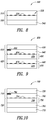
- Figure 5 shows an optical stack (200) according to an example not corresponding to the invention as defined in the claims comprising a substrate (210), an undercoat layer (220) deposited on the substrate (210), the undercoat layer (220) including one or more photo-stabilizers (not shown); a nanostructure layer (230) having a plurality of silver nanostructures (234), and an overcoat layer (240) deposited on the nanostructure layer (230).
- the overcoat layer (240) is further bonded, via an OCA layer (250) to a protective film (260).
- the photo-stabilizers in the OCA layer can have a significant impact.
- the OCA layers are generally the thickest layers in an optical stack, they allow for a higher total content (e.g. in mg/m 2 ) of the photo-stabilizers.
- the nanostructure layers considered herein typically have total thickness of 100-200 nm, whereas OCA layers have thicknesses ranging from 25 ⁇ m to 250 ⁇ m.
- a large total amount of the additive can be included in the OCA. This is especially beneficial if the additive is consumed while carrying out its protective function.
- a specific embodiment provides an optical stack having a nanostructure layer and an OCA layer in contact with the nanostructure layer, wherein the OCA layer includes an ascorbate.
- the OCA layer comprises 0.1-1% of sodium ascorbate.
- the photo-stabilizers such as terpenes and certain resin tackifiers
- the liquid photo-stabilizer can be combined directly with a pre-made OCA (e.g., in its commercial form).
- the pre-made OCA may be sprayed with, dipped in or otherwise contact the liquid photo-stabilizer. After a period of allowing the liquid to infiltrate, the residue liquid on the surface of the OCA layer can be wiped off or spun off.
- OCAs examples include those that are commercially available from 3M Company under product numbers 8146-2, 8142KCL, 8172CL, 8262N; Nitto Denko Corporation under the product number CS9662LS; and Hitachi Chemical Corporation under the product number TE7070.
- the above technique is not limited to commercial forms of OCA.
- Any adhesive layers may be similarly incorporated with one or more photo-stabilizers as described herein.
- a transparent conductor may also be treated with a photo-stabilizer (e.g., Figure 6 ) in the same manner as the OCA.
- the photo-stabilizer may contact (spray or dip) the transparent conductor for a period of time to allow for the diffusion of the photo-stabilizer into the transparent conductor.
- the photo-stabilizers may also be first in the form of a dispersion that contains a volatile solvent (e.g., alcohols, acetone, water and the like). The dispersion is then combined with the coating solution prior to coating. Alternatively, the dispersion may be coated in a separate step independently from the other coating steps for forming the optical stack. The volatile solvent is thereafter removed along with other volatile solvent(s) in the coating solution.
- the dispersion may contact a layer (OCA or transparent conductor) for a period of time to allow for the diffusion of the photo-stabilizer into the layer.
- the photo-stabilizer can also be combined directly with any film-forming coating solution prior to coating.
- the photo-stabilizer maybe combined with a coating solution of the silver nanostructures, or a coating solution of overcoat or undercoat, or a coating solution for forming an adhesive layer.
- an optical stack comprising a substrate, a transparent conductor including a plurality of interconnecting silver nanostructures; an optically clear adhesive layer, wherein at least one of the transparent conductor and the optically clear adhesive layer incorporates one or more photo-stabilizers.
- the photo-stabilizer may be an alkene (e.g., a terpene), an ascorbate, a hindered phenol, a tetrazole or triazole, a phosphine, a thioether or metals as described herein.
- the antioxidant may be present in each layer above a threshold concentration to adequately provide a barrier for oxygen.
- the concentration may be typically no more than 5 w/w% of the layer, more typically, no more than 1 w/w%, or no more than 0.5 w/w%, or no more than 0.1 w/w% or no more than 0.05 w/w%.
- concentrations may be needed depending on the location or specific layer in which the anti-oxidant is present.
- Oxygen barriers are physical barriers (e.g., film or edge seals) that minimize or prohibit the permeation of the atmospheric gas, 21% of which is oxygen.
- gas barrier and “oxygen barrier” are used interchangeably herein.
- either the first substack or the second substack of the optical stack of Figure 1 may include a gas barrier.
- both the first substack and the second substack include a gas barrier, respectively, thus creating at least a partial encapsulation around the nanostructure layer.
- a gas or oxygen barrier film may be formed of a material that has low oxygen transmission rate (OTR).
- OTR is a measure of permeability of oxygen through a medium (e.g., a film) at the atmospheric pressure. OTR is also a function of temperature.
- a "low-OTR" layer has an OTR of no more than 10 cc/m2 ⁇ d ⁇ atm at 25°C, or no more than 5 cc/m2 ⁇ d ⁇ atm at 25°C, or no more than 3 cc/m2 ⁇ d ⁇ atm at 25°C, or no more than 1 cc/m2 ⁇ d ⁇ atm at 25°C.
- the gas barrier layer in each of the substack should render the substack to have an OTR of no more than 5 cc/m2 ⁇ d ⁇ atm at 25°C (when measured in isolation).
- Glass, plastic cover lens are natural gas barriers.
- Certain polymers and adhesives, such as polyvinyl alcohol (PVOH) and polyvinylidene chloride (PVDC) have low OTR.
- rigid substrates such as glass are oxygen barriers, they are not within the meaning of the oxygen barrier film, as used herein, which is flexible.
- Film components in an optical stack that are not naturally low in OTR may be coated with one or more low OTR coating layers.
- Low OTR coating layers may include an inorganic layer (metallic or ceramic), such as sputtered SiO 2 , AlO 2 or ITO.
- the inorganic layer may further include antireflection layers.
- SiO 2 -coated films may be obtained from commercial vendors (e.g., CPT001 with an OTR of 2.3 cc/m2 ⁇ d ⁇ atm and CPT002 with an OTR of 1.1 cc/m2 ⁇ d ⁇ atm, from Celplast).
- Substrates such as PET, TCA may also be coated or sputtered with an ITO layer.
- the low-OTR coatings may also be an organic layer, such as PVOH, PVDC, or a suitable hardcoat.
- a further example of a low-OTR coating may be a hybrid coating of low-OTR organic and inorganic layer, as described above.
- FIG. 6 shows an optical stack in which the substacks are more specifically delineated.
- An optical stack (600) comprises a first substack (610) and a second substack (620).
- the first substack (610) includes a first substrate (630) and a first OCA layer (640).
- the first substack (610) is bonded, via the OCA layer (640), to the second substack (620) which includes a first conductive film (650) having a first plurality of nanostructures (654) deposited on a second substrate (656).
- the first conductive film (650) may be, for example, the ClearOhm ® film by Cambrios Technologies Corporation.
- the first substrate (630) maybe glass, which also functions as an oxygen barrier.
- the nanostructures (654 and 674) are encapsulated between two oxygen barriers (630 and 676).
- oxygen barrier is shown as the outermost layer in the optical stacks of Figures 8 and 9 , it should be understood that the oxygen barrier can be in other locations of the optical stacks, depending on the configuration of the other layers in each of the substack, and in particular, the location of a nanostructure layer. In certain embodiments, two or more oxygen barriers may be present in one optical stack.
- FIG 10 shows another example not corresponding to the invention as defined in the claims.
- the optical stack (700) is shown as including a first substack (710) and a second substack (720).
- the first substack (710) includes a first substrate (730) and a first OCA layer (740).
- the first substack (710) is bonded, via the first OCAlayer (740), to the second substack (720) which includes a conductive film (750) having a plurality of nanostructures (754) deposited on a second substrate (756), which could be a PET film or a first oxygen barrier film.
- the second stack (720) further includes a second OCA layer (760), which in turn is bonded to a second oxygen barrier film (770).
- the optical stack (700) is shown with a deco frame (780).
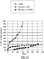
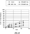
- Table 3 shows examples of suitable oxygen barrier films that may be used in any of the configurations as described herein.
- Table 3 also shows time to edge failure in optical stacks configured according to Figure 10 (in which the second substrate 756 is a PET film).
- the time to edge failure correlates to the OTR of the barrier film. More specifically, the lower the OTR of the oxygen barrier film, the longer the time to edge failure, i.e., the better stability of the optical stack. All of the optical stacks having oxygen barrier films showed enhanced stability compared to a control stack that has no barrier film.
- the optical stack may comprise at least one edge seal.
- the optical stack may comprise two, three or up to four edge seals.
- the edge seals are also oxygen barriers that encapsulate the nanowire layer, thereby preventing atmospheric gas such as oxygen from infiltrating the optical stack.
- the edge seal may be applied to any of the configurations described above, including the generic stack that does not have any other oxygen barriers within the stack.
- Figure 11 shows an optical stack with edge seals (two are shown). More specifically, an optical stack (800) is shown as including a first substack (810), a second substack (820), a nanostructure layer (830) disposed between the first substack (810) and the second substack (820), the nanostructure layer including a plurality of silver nanostructures (834).
- the optical stack further comprises a first vertical edge (840) covered by a first edge seal (844) and a second vertical edge (850) covered by a second edge seal (854).
- the optical stack may be laminated with a film having a barrier coating (e.g., sputtered ceramic layer) on a back side of the stack.
- a barrier coating e.g., sputtered ceramic layer
- the nanostructure film may be stored in a nitrogen-purged container during light exposure.
- accelerated light condition refers to an artificial or testing condition that exposes the optical stack to continuous and intense simulated light. Often, the accelerated light condition can be controlled to simulate the amount of light exposure that the optical stack is subjected to during a normal service life of a given device.
- the light intensity is typically significantly elevated compared to the operating light intensity of the given device; the duration of the light exposure for testing the reliability of the conductive films can therefore be significantly compressed compared to the normal service life of the same device.
- light intensity is measured in Lumens, which is a unit of luminous flux. Under an accelerated light condition, the light is about 30 to 100 times more intense than the light condition of a device.
- the accelerated light tests can be used to evaluate the effectiveness of a photo-stabilizer.
- metal nanostructures generally refer to electrically conductive nano-sized structures, at least one dimension of which (i.e., width or diameter) is less than 500 nm; more typically, less than 100 nm or 50 nm.
- width or diameter of the nanostructures are in the range of 10 to 40 nm, 20 to 40 nm, 5 to 20 nm, 10 to 30 nm, 40 to 60 nm, 50 to 70 nm.
- the nanostructures can be of any shape or geometry.
- One way for defining the geometry of a given nanostructure is by its "aspect ratio," which refers to the ratio of the length and the width (or diameter) of the nanostructure.
- Typical isotropic or substantially isotropic nanostructures include nanoparticles.
- the nanostructures are anisotropically shaped (i.e. aspect ratio ⁇ 1).
- the anisotropic nanostructure typically has a longitudinal axis along its length.
- Exemplary anisotropic nanostructures include nanowires (solid nanostructures having aspect ratio of at least 10, and more typically, at least 50), nanorod (solid nanostructures having aspect ratio of less than 10) and nanotubes (hollow nanostructures).
- Metal nanostructures are typically a metallic material, including elemental metal (e . g ., transition metals) or a metal compound ( e . g ., metal oxide).
- the metallic material can also be a bimetallic material or a metal alloy, which comprises two or more types of metal. Suitable metals include, but are not limited to, silver, gold, copper, nickel, gold-plated silver, platinum and palladium. It should be noted that although the present disclosure describes primarily nanowires ( e . g ., silver nanowires), any nanostructures within the above definition can be equally employed.
- metal nanostructures are metal nanowires that have aspect ratios in the range of 10 to 100,000. Larger aspect ratios can be favored for obtaining a transparent conductor layer since they may enable more efficient conductive networks to be formed while permitting lower overall density of wires for a high transparency. In other words, when conductive nanowires with high aspect ratios are used, the density of the nanowires that achieves a conductive network can be low enough that the conductive network is substantially transparent.
- Metal nanowires can be prepared by known methods in the art.
- silver nanowires can be synthesized through solution-phase reduction of a silver salt (e.g ., silver nitrate) in the presence of a polyol ( e . g ., ethylene glycol) and poly(vinyl pyrrolidone).
- a silver salt e.g ., silver nitrate
- a polyol e.g ., ethylene glycol
- poly(vinyl pyrrolidone) e.g ethylene glycol
- Large-scale production of silver nanowires of uniform size can be prepared and purified according to the methods described in U.S. Published Application Nos. 2008/0210052 , 2011/0024159 , 2011/0045272 , and 2011/0048170 , all in the name of Cambrios Technologies Corporation, the assignee of the present disclosure.
- a nanostructure layer is a conductive network of interconnecting metal nanostructures (e.g., silver nanowire) that provide the electrically conductive media of a transparent conductor. Since electrical conductivity is achieved by electrical charge percolating from one metal nanostructure to another, sufficient metal nanowires must be present in the conductive network to reach an electrical percolation threshold and become conductive.
- the surface conductivity of the conductive network is inversely proportional to its surface resistivity, sometimes referred to as sheet resistance, which can be measured by known methods in the art.
- electrically conductive or simply “conductive” corresponds to a surface resistivity of no more than 10 4 ⁇ / ⁇ , or more typically, no more than 1,000 ⁇ / ⁇ , or more typically no more than 500 ⁇ / ⁇ , or more typically no more than 200 ⁇ / ⁇ .
- the surface resistivity depends on factors such as the aspect ratio, the degree of alignment, degree of agglomeration and the resistivity of the interconnecting metal nanostructures.
- the metal nanostructures may form a conductive network on a substrate without a binder.
- a binder may be present that facilitates adhesion of the nanostructures to the substrate.
- Suitable binders include optically clear polymers including, without limitation: polyacrylics such as polymethacrylates (e.g., poly(methyl methacrylate)), polyacrylates and polyacrylonitriles, polyvinyl alcohols, polyesters (e.g., polyethylene terephthalate (PET), polyester naphthalate, and polycarbonates), polymers with a high degree of aromaticity such as phenolics or cresolformaldehyde (Novolacs ® ), polystyrenes, polyvinyltoluene, polyvinylxylene, polyimides, polyamides, polyamideimides, polyetherimides, polysulfides, polysulfones, polyphenylenes, and polyphenyl ethers, polyurethane (
- polypropylene polymethylpentene, and cyclic olefins
- ABS acrylonitrile-butadiene-styrene copolymer
- cellulosics cellulosics
- silicones and other silicon-containing polymers e.g.
- polysilsesquioxanes and polysilanes polysilsesquioxanes and polysilanes), polyvinylchloride (PVC), polyacetates, polynorbornenes, synthetic rubbers (e.g., EPR, SBR, EPDM), and fluoropolymers (e.g., polyvinylidene fluoride, polytetrafluoroethylene (TFE) or polyhexafluoropropylene), copolymers of fluoro-olefin and hydrocarbon olefin ( e.g., Lumiflon ® ), and amorphous fluorocarbon polymers or copolymers ( e . g ., CYTOP ® by Asahi Glass Co., or Teflon ® AF by Du Pont).
- PVC polyvinylchloride
- polyacetates polynorbornenes
- synthetic rubbers e.g., EPR, SBR, EPDM
- “Substrate” refers to a non-conductive material onto which the metal nanostructure is coated or laminated.
- the substrate can be rigid or flexible.
- the substrate can be clear or opaque.
- Suitable rigid substrates include, for example, glass, polycarbonates, acrylics, and the like.
- Suitable flexible substrates include, but are not limited to: polyesters ( e.g ., polyethylene terephthalate (PET), polyester naphthalate, and polycarbonate), polyolefins ( e . g ., linear, branched, and cyclic polyolefins), polyvinyls ( e .
- polyvinyl chloride polyvinylidene chloride, polyvinyl acetals, polystyrene, polyacrylates, and the like
- cellulose ester bases e . g ., cellulose triacetate, cellulose acetate
- polysulphones such as polyethersulphone, polyimides, silicones and other conventional polymeric films. Additional examples of suitable substrates can be found in, e.g., U.S. Patent No. 6,975,067 .
- the optical transparence or clarity of the transparent conductor can be quantitatively defined by parameters including light transmission and haze.
- Light transmission (or “light transmissivity”) refers to the percentage of an incident light transmitted through a medium.
- the light transmission of the conductive layer is at least 80% and can be as high as 98%.
- Performance-enhancing layers such as an adhesive layer, anti-reflective layer, or anti-glare layer, may further contribute to reducing the overall light transmission of the transparent conductor.
- the light transmission (T%) of the transparent conductors can be at least 50%, at least 60%, at least 70%, or at least 80% and maybe as high as at least 91% to 92%, or at least 95%.
- Haze is a measure of light scattering. It refers to the percentage of the quantity of light separated from the incident light and scattered during transmission. Unlike light transmission, which is largely a property of the medium, haze is often a production concern and is typically caused by surface roughness and embedded particles or compositional heterogeneities in the medium. Typically, haze of a conductive film can be significantly impacted by the diameters of the nanostructures. Nanostructures of larger diameters ( e . g ., thicker nanowires) are typically associated with a higher haze.
- the patterned transparent conductors according to the present disclosure are prepared by coating a nanostructure-containing coating composition on a non-conductive substrate.
- the metal nanowires are typically dispersed in a volatile liquid to facilitate the coating process.
- a volatile liquid to facilitate the coating process.
- the metal nanowires are dispersed in water, an alcohol, a ketone, ethers, hydrocarbons or an aromatic solvent (benzene, toluene, xylene, etc.). More preferably, the liquid is volatile, having a boiling point of no more than 200°C, no more than 150°C, or no more than 100°C.
- a nanowire dispersion, or "ink” includes, by weight, from 0.0025% to 0.1% surfactant (e.g., a preferred range is from 0.0025% to 0.05% for Zonyl ® FSO-100), from 0.02% to 4% viscosity modifier (e.g., a preferred range is 0.02% to 0.5% for HPMC), from 94.5% to 99.0% solvent and from 0.05% to 1.4% metal nanowires.
- surfactant e.g., a preferred range is from 0.0025% to 0.05% for Zonyl ® FSO-100
- viscosity modifier e.g., a preferred range is 0.02% to 0.5% for HPMC
- Suitable surfactants include Zonyl ® FSN, Zonyl ® FSO, Zonyl ® FSH, Triton (x100, x114, x45), Dynol (604, 607), n-Dodecyl b-D-maltoside and Novek.
- suitable viscosity modifiers include hydroxypropyl methyl cellulose (HPMC), methyl cellulose, xanthan gum, polyvinyl alcohol, carboxy methyl cellulose, and hydroxy ethyl cellulose.
- suitable solvents include water and isopropanol.
- the nanowire concentration in the dispersion can affect or determine parameters such as thickness, conductivity (including surface conductivity), optical transparency, and mechanical properties of the nanowire network layer.
- the percentage of the solvent can be adjusted to provide a desired concentration of the nanowires in the dispersion.
- the relative ratios of the other ingredients can remain the same.
- the ratio of the surfactant to the viscosity modifier is preferably in the range of about 80 to about 0.01; the ratio of the viscosity modifier to the metal nanowires is preferably in the range of about 5 to about 0.000625; and the ratio of the metal nanowires to the surfactant is preferably in the range of about 560 to about 5.
- the ratios of components of the dispersion may be modified depending on the substrate and the method of application used.
- the preferred viscosity range for the nanowire dispersion is between about 1 and 100 cP.
- the volatile liquid is removed by evaporation.
- the evaporation can be accelerated by heating (e.g., baking).
- the resulting nanowire network layer may require post-treatment to render it electrically conductive. This post-treatment can be a process step involving exposure to heat, plasma, corona discharge, UV-ozone, or pressure as described below.
- the coating composition is coated on a substrate by, for example, sheet coating, web-coating, printing, and lamination, to provide a transparent conductor. Additional information for fabricating transparent conductors from conductive nanostructures is disclosed in, for example, U.S. Published Patent Application No. 2008/0143906 , and 2007/0074316 , in the name of Cambrios Technologies Corporation.
- Silver nanowires were synthesized by the reduction of silver nitrate dissolved in ethylene glycol in the presence of poly(vinyl pyrrolidone) (PVP) following the "polyol” method described in, e.g., Y. Sun, B. Gates, B. Mayers, & Y. Xia, "Crystalline silver nanowires by soft solution processing", Nanoletters, (2002), 2(2) 165-168 .
- PVP poly(vinyl pyrrolidone)
- a control stack was made by (1) preparing a transparent conductor of silver nanostructure conductive network deposited on a PET film (e.g., ClearOhm ® film); (2) laminating an OCA on glass, and (3) laminating the transparent conductor on the OCA/glass, the silver nanostructures being in contact with the OCA.
- a PET film e.g., ClearOhm ® film
- An optical stack was prepared in the same manner as in Example 1. It was then exposed to UV radiation using a Fusion system equipped with an H-bulb, for 3 passes at 3ft/min on one side of the stack, then 3 passes at 3ft/min on the other side.
- An optical stack was prepared by first laminating an OCA layer on a glass substrate, exposing the OCA to a puddle of terpineol then spinning excess off, followed by baking at 80°C for 60 seconds in an oven.
- the OCA layer was first treated with limonene a similar manner as terpineol. The liquid limonene was allowed to puddle on the OCA layer for about 60 seconds. Limonene was then spun off and dried in a nitrogen atmosphere. Thereafter, the OCA/glass was laminated on a silver nanostructure-based transparent conductor, the OCA layer being in contact with the silver nanostructure. The starting resistance of the transparent conductor was less than 500 ⁇ /sq. The film stack was then exposed to an accelerated light test (200mW/cm 2 measured at 365nm).
- the film stack exposed to limonene had a resistance drift (as measured using a non-contact method) below 30% out to 800 hours and below 40% out to almost 1000 hours, indicating that limonene is an effective photo-stabilizer that is capable of forestalling silver corrosion upon light exposure.
- a transparent conductor of silver nanostructures was first formed on PET ("NW film on PET").
- a 1% dispersion of 1-phenyl-1H-tetrazole-5-thiol (PTZT) in methanol was prepared.
- the NW film on PET was then soaked in the PTZT solution before drying with nitrogen and wiping off the excess.
- the treated transparent conductor was then laminated to a glass substrate using an OCA
- the starting resistance of the transparent conductor was less than 500 ⁇ /sq.
- the accelerated light test (200mW/cm 2 measured at 365nm) is shown in Figure13 .
- the transparent conductor treated with PTZT shows less than 10% drift after 200 hours, whereas the untreated transparent conductor became non-conductive after 150 hours. The result indicates that PTZT was effective in preventing photo corrosion of the silver nanostructures.
- Figure 14 shows the accelerated light tests of PTZT-treated NW film and limonene-treated OCA film as compared to the untreated optical stack. As shown, both photo-stabilizers were comparably effective in reducing or preventing photo corrosion.
- FIG 15 shows the accelerated light tests of PTZT-treated NW film and PTZT-treated OCA film. As shown, PTZT was comparably effective at different locations of an optical stack (e.g., the NW film or OCA film).
- an optical stack e.g., the NW film or OCA film.
- FIG. 16 shows that the BTA-treated transparent conductors are more stable than transparent conductors untreated by BTA under the accelerated light condition.
Landscapes
- Engineering & Computer Science (AREA)
- Physics & Mathematics (AREA)
- Plasma & Fusion (AREA)
- Microelectronics & Electronic Packaging (AREA)
- Laminated Bodies (AREA)
- Chemical & Material Sciences (AREA)
- Nonlinear Science (AREA)
- General Physics & Mathematics (AREA)
- General Engineering & Computer Science (AREA)
- Theoretical Computer Science (AREA)
- Non-Insulated Conductors (AREA)
- Mathematical Physics (AREA)
- Conductive Materials (AREA)
- Crystallography & Structural Chemistry (AREA)
- Optics & Photonics (AREA)
- Dispersion Chemistry (AREA)
- Spectroscopy & Molecular Physics (AREA)
- Human Computer Interaction (AREA)
Claims (12)
- Optischer Stapel (400), der Folgendes umfasst:ein erstes Substrat (410);eine Nanostrukturschicht mit einer Vielzahl von Silber-Nanostrukturen (424) auf dem ersten Substrat (410), wobei die Nanostrukturschicht eine Dicke von 100 nm bis 200 nm aufweist;eine optisch klare Klebstoffschicht (OCA) (430), die auf der Nanostrukturschicht (420) abgeschieden ist;wobei die Silber-Nanostrukturen (424) in Kontakt mit der OCA-Schicht (430) sind undwobei die OCA-Schicht (430) einen oder mehrere Fotostabilisatoren umfasst;dadurch gekennzeichnet, dass die OCA-Schicht (430) eine Dicke von 25 µm bis 250 µm aufweist.
- Optischer Stapel nach Anspruch 1, wobei die Silber-Nanostrukturen (424) untereinander verbindende Silber-Nanodrähte sind.
- Optischer Stapel nach einem der Ansprüche 1 oder 2, wobei der Fotostabilisator ein Alken ist.
- Optischer Stapel nach Anspruch 3, wobei der Fotostabilisator ein Terpen ist.
- Optischer Stapel nach Anspruch 4, wobei der Fotostabilisator ein Limonen ist.
- Optischer Stapel nach Anspruch 4, wobei der Fotostabilisator Terpineol ist.
- Optischer Stapel nach Anspruch 3, wobei der Fotostabilisator ein Tetrazol ist.
- Optischer Stapel nach Anspruch 7, wobei der Fotostabilisator ein 1-Phenyl-1H-tetrazol-5-thiol ist.
- Optischer Stapel nach Anspruch 3, wobei der Fotostabilisator ein Triazol, ein Phosphin oder ein Thioether ist.
- Optischer Stapel nach Anspruch 3, wobei der Fotostabilisator ein gehindertes Phenol ist, besonders bevorzugt butyliertes Hydroxytoluol, Alkylgallat, tertiär-butyliertes Hydrochinon, Vitamin E, butyliertes Hydroxyanisol.
- Optischer Stapel nach Anspruch 3, wobei der Fotostabilisator ein Fotodesensibilisator ist, der unter einem Cadmiumsalz, einem Zinksalz oder einem Rhodiumsalz ausgewählt ist.
- Optischer Stapel nach Anspruch 3, wobei der Fotostabilisator Natriumascorbat oder Potassiumascorbat ist, wobei die OCA-Schicht (430) vorzugsweise etwa 0,1 Gew.-% Natriumascorbat enthält.
Priority Applications (1)
| Application Number | Priority Date | Filing Date | Title |
|---|---|---|---|
| EP19196099.6A EP3598185A3 (de) | 2013-02-15 | 2014-02-14 | Verfahren zur integration von transparenten leitern auf silbernanodrahtbasis in elektronische vorrichtungen |
Applications Claiming Priority (4)
| Application Number | Priority Date | Filing Date | Title |
|---|---|---|---|
| US201361765420P | 2013-02-15 | 2013-02-15 | |
| US13/840,864 US10720257B2 (en) | 2013-02-15 | 2013-03-15 | Methods to incorporate silver nanowire-based transparent conductors in electronic devices |
| US201461928891P | 2014-01-17 | 2014-01-17 | |
| PCT/US2014/016612 WO2014127297A1 (en) | 2013-02-15 | 2014-02-14 | Methods to incorporate silver nanowire-based transparent conductors in electronic devices |
Related Child Applications (2)
| Application Number | Title | Priority Date | Filing Date |
|---|---|---|---|
| EP19196099.6A Division-Into EP3598185A3 (de) | 2013-02-15 | 2014-02-14 | Verfahren zur integration von transparenten leitern auf silbernanodrahtbasis in elektronische vorrichtungen |
| EP19196099.6A Division EP3598185A3 (de) | 2013-02-15 | 2014-02-14 | Verfahren zur integration von transparenten leitern auf silbernanodrahtbasis in elektronische vorrichtungen |
Publications (2)
| Publication Number | Publication Date |
|---|---|
| EP2956807A1 EP2956807A1 (de) | 2015-12-23 |
| EP2956807B1 true EP2956807B1 (de) | 2021-11-03 |
Family
ID=51354595
Family Applications (2)
| Application Number | Title | Priority Date | Filing Date |
|---|---|---|---|
| EP14708390.1A Not-in-force EP2956807B1 (de) | 2013-02-15 | 2014-02-14 | Verfahren zur integration von transparenten leitern auf silbernanodrahtbasis in elektronischen vorrichtungen |
| EP19196099.6A Withdrawn EP3598185A3 (de) | 2013-02-15 | 2014-02-14 | Verfahren zur integration von transparenten leitern auf silbernanodrahtbasis in elektronische vorrichtungen |
Family Applications After (1)
| Application Number | Title | Priority Date | Filing Date |
|---|---|---|---|
| EP19196099.6A Withdrawn EP3598185A3 (de) | 2013-02-15 | 2014-02-14 | Verfahren zur integration von transparenten leitern auf silbernanodrahtbasis in elektronische vorrichtungen |
Country Status (7)
| Country | Link |
|---|---|
| EP (2) | EP2956807B1 (de) |
| JP (1) | JP6588829B2 (de) |
| KR (1) | KR102185129B1 (de) |
| CN (1) | CN105283782B (de) |
| HK (1) | HK1219309A1 (de) |
| SG (2) | SG10201706567VA (de) |
| WO (1) | WO2014127297A1 (de) |
Families Citing this family (2)
| Publication number | Priority date | Publication date | Assignee | Title |
|---|---|---|---|---|
| JP6938856B2 (ja) * | 2016-05-24 | 2021-09-22 | 大日本印刷株式会社 | 導電性基材、導電膜転写フィルム、及び表示装置 |
| CN108621753A (zh) | 2017-03-24 | 2018-10-09 | 凯姆控股有限公司 | 平面加热结构 |
Citations (1)
| Publication number | Priority date | Publication date | Assignee | Title |
|---|---|---|---|---|
| US20120063952A1 (en) * | 2010-09-10 | 2012-03-15 | Hong Keith C | Uv resistant clear laminates |
Family Cites Families (37)
| Publication number | Priority date | Publication date | Assignee | Title |
|---|---|---|---|---|
| US2453087A (en) | 1946-11-07 | 1948-11-02 | Gen Aniline & Film Corp | Photographic developers containing tetrazolyl disulfides as antifogging agents |
| US2588538A (en) | 1948-08-06 | 1952-03-11 | Ilford Ltd | Stabilizers in photographic emulsions and developers |
| US2839405A (en) | 1955-03-08 | 1958-06-17 | Eastman Kodak Co | Inorganic salt antifoggants for photographic emulsions |
| GB1183317A (en) | 1966-07-01 | 1970-03-04 | Agfa Gevaert Nv | Selectively Desensitized Silver Halide Emulsion Materials |
| US3579333A (en) | 1968-07-18 | 1971-05-18 | Polaroid Corp | Multicolor diffusion transfer photographic products and processes with a developing composition comprising a desensitizing agent |
| AR204386A1 (es) | 1971-03-16 | 1976-02-06 | Minnesota Mining & Mfg | Emulsion fotografica a base de haluros de plata |
| GB1402819A (en) | 1972-10-13 | 1975-08-13 | Du Pont | Thio-substituted succinimides and their use in light sensitive photographic material |
| JPS60443A (ja) | 1983-06-17 | 1985-01-05 | Fuji Photo Film Co Ltd | 再反転ネガ像の抑制された直接ポジハロゲン化銀写真感光材料 |
| US4666827A (en) | 1984-07-16 | 1987-05-19 | Mitsubishi Paper Mills, Ltd. | Silver halide photographic emulsion |
| JPS61240573A (ja) * | 1985-04-18 | 1986-10-25 | Toshiba Corp | アルカリ電池 |
| US4908273A (en) * | 1987-03-24 | 1990-03-13 | Ciba-Geigy Corporation | Multi-layer, heat-curable adhesive film |
| EP0702265A1 (de) | 1994-09-13 | 1996-03-20 | Minnesota Mining And Manufacturing Company | Photographisches Silberhalogenidmaterial, das eine Mercaptotetrazolverbindung enthält |
| US6043013A (en) | 1998-01-29 | 2000-03-28 | Eastman Kodak Company | Color photographic element containing elemental silver and heterocyclic thiol in a non-light sensitive layer |
| JP2003041218A (ja) * | 2000-08-31 | 2003-02-13 | Matsushita Electric Ind Co Ltd | 導電性接着剤およびこれを用いた実装構造体 |
| US7261839B2 (en) * | 2002-01-22 | 2007-08-28 | Northern Technologies International Corp. | Tarnish inhibiting composition and article containing it |
| US6975067B2 (en) | 2002-12-19 | 2005-12-13 | 3M Innovative Properties Company | Organic electroluminescent device and encapsulation method |
| JP2006272876A (ja) * | 2005-03-30 | 2006-10-12 | Takiron Co Ltd | 導電体 |
| JP5546763B2 (ja) * | 2005-08-12 | 2014-07-09 | カンブリオス テクノロジーズ コーポレイション | ナノワイヤに基づく透明導電体 |
| US8454721B2 (en) | 2006-06-21 | 2013-06-04 | Cambrios Technologies Corporation | Methods of controlling nanostructure formations and shapes |
| TWI426531B (zh) | 2006-10-12 | 2014-02-11 | Cambrios Technologies Corp | 以奈米線為主之透明導體及其應用 |
| US8885135B2 (en) * | 2007-10-29 | 2014-11-11 | Samsung Electronics Co., Ltd. | Nanostructure-film LCD devices |
| JP2011515510A (ja) | 2008-02-26 | 2011-05-19 | カンブリオス テクノロジーズ コーポレイション | 導電性特徴をスクリーン印刷するための方法および組成物 |
| WO2010026571A2 (en) * | 2008-09-02 | 2010-03-11 | Ramot At Tel-Aviv University Ltd. | Metal nanowire thin-films |
| JP5098957B2 (ja) * | 2008-10-31 | 2012-12-12 | コニカミノルタホールディングス株式会社 | 有機光電変換素子 |
| JP2010153153A (ja) * | 2008-12-25 | 2010-07-08 | Mitsubishi Paper Mills Ltd | 光透過性導電性材料 |
| EA024263B1 (ru) * | 2009-03-13 | 2016-09-30 | Грин Сос Энерджи Ллк | Экстракция углеводородов из углеводородсодержащих материалов и/или переработка углеводородсодержащих материалов |
| US20110024159A1 (en) | 2009-05-05 | 2011-02-03 | Cambrios Technologies Corporation | Reliable and durable conductive films comprising metal nanostructures |
| EP2430639A1 (de) * | 2009-05-05 | 2012-03-21 | Cambrios Technologies Corporation | Zuverlässige und beständige leitende folien mit metallnanostrukturen |
| JP5472299B2 (ja) * | 2009-06-24 | 2014-04-16 | コニカミノルタ株式会社 | 透明電極、該透明電極に用いられる導電性繊維の精製方法、及び有機エレクトロルミネッセンス素子 |
| EP2470610A1 (de) | 2009-08-24 | 2012-07-04 | Cambrios Technologies Corporation | Reinigung von metallnanostrukturen für verbesserte trübung in daraus hergestellten transparenten leitern |
| JP2013503260A (ja) | 2009-08-25 | 2013-01-31 | カンブリオス テクノロジーズ コーポレイション | 金属ナノワイヤの形態を制御する方法 |
| JP2011150316A (ja) * | 2009-12-21 | 2011-08-04 | Konica Minolta Opto Inc | 太陽熱発電用フィルムミラー、その製造方法及び太陽熱発電用反射装置 |
| EP2524380B1 (de) | 2010-01-15 | 2021-06-23 | Cambrios Film Solutions Corporation | Transparente leiter mit geringer opazität |
| EP2547735B1 (de) * | 2010-03-19 | 2016-03-16 | Carestream Health, Inc. | Antikorrosionsmittel für eine transparente leitende folie |
| JP2011222453A (ja) * | 2010-04-14 | 2011-11-04 | Sumitomo Bakelite Co Ltd | 導電膜付き基材 |
| US20120104374A1 (en) | 2010-11-03 | 2012-05-03 | Cambrios Technologies Corporation | Coating compositions for forming nanocomposite films |
| JP2015069508A (ja) * | 2013-09-30 | 2015-04-13 | 凸版印刷株式会社 | タッチパネル |
-
2014
- 2014-02-14 EP EP14708390.1A patent/EP2956807B1/de not_active Not-in-force
- 2014-02-14 CN CN201480019686.7A patent/CN105283782B/zh active Active
- 2014-02-14 JP JP2015558171A patent/JP6588829B2/ja active Active
- 2014-02-14 SG SG10201706567VA patent/SG10201706567VA/en unknown
- 2014-02-14 WO PCT/US2014/016612 patent/WO2014127297A1/en active Application Filing
- 2014-02-14 EP EP19196099.6A patent/EP3598185A3/de not_active Withdrawn
- 2014-02-14 SG SG11201506221SA patent/SG11201506221SA/en unknown
- 2014-02-14 KR KR1020157025061A patent/KR102185129B1/ko active IP Right Grant
-
2016
- 2016-06-21 HK HK16107186.1A patent/HK1219309A1/zh unknown
Patent Citations (1)
| Publication number | Priority date | Publication date | Assignee | Title |
|---|---|---|---|---|
| US20120063952A1 (en) * | 2010-09-10 | 2012-03-15 | Hong Keith C | Uv resistant clear laminates |
Also Published As
| Publication number | Publication date |
|---|---|
| SG11201506221SA (en) | 2015-09-29 |
| JP6588829B2 (ja) | 2019-10-09 |
| CN105283782A (zh) | 2016-01-27 |
| JP2016515280A (ja) | 2016-05-26 |
| KR20150119255A (ko) | 2015-10-23 |
| HK1219309A1 (zh) | 2017-03-31 |
| WO2014127297A1 (en) | 2014-08-21 |
| EP2956807A1 (de) | 2015-12-23 |
| KR102185129B1 (ko) | 2020-12-02 |
| EP3598185A2 (de) | 2020-01-22 |
| SG10201706567VA (en) | 2017-09-28 |
| CN105283782B (zh) | 2019-09-06 |
| EP3598185A3 (de) | 2020-04-22 |
Similar Documents
| Publication | Publication Date | Title |
|---|---|---|
| US10971277B2 (en) | Methods to incorporate silver nanowire-based transparent conductors in electronic devices | |
| US11137863B2 (en) | Silver nanostructure-based optical stacks and touch sensors with UV protection | |
| US20230250535A1 (en) | Noble metal coated silver nanowires | |
| JP6644684B2 (ja) | 金属ナノワイヤおよびポリマーバインダーを主成分とする透明導電性コーティング、その溶液処理、およびパターン化方法 | |
| US8174667B2 (en) | Nanowire-based transparent conductors and applications thereof | |
| US20130001478A1 (en) | Reliable and durable conductive films comprising metal nanostructures | |
| KR102581899B1 (ko) | 투명 전극 및 이를 포함하는 소자 | |
| EP2430639A1 (de) | Zuverlässige und beständige leitende folien mit metallnanostrukturen | |
| US20160122562A1 (en) | Stable transparent conductive elements based on sparse metal conductive layers | |
| EP2539943A1 (de) | Transparente leiter auf nanodrahtbasis und verfahren zu ihrer strukturierung | |
| US20200350091A1 (en) | Methods to incorporate silver nanowire-based transparent conductors in electronic devices | |
| EP2956807B1 (de) | Verfahren zur integration von transparenten leitern auf silbernanodrahtbasis in elektronischen vorrichtungen |
Legal Events
| Date | Code | Title | Description |
|---|---|---|---|
| PUAI | Public reference made under article 153(3) epc to a published international application that has entered the european phase |
Free format text: ORIGINAL CODE: 0009012 |
|
| 17P | Request for examination filed |
Effective date: 20150914 |
|
| AK | Designated contracting states |
Kind code of ref document: A1 Designated state(s): AL AT BE BG CH CY CZ DE DK EE ES FI FR GB GR HR HU IE IS IT LI LT LU LV MC MK MT NL NO PL PT RO RS SE SI SK SM TR |
|
| AX | Request for extension of the european patent |
Extension state: BA ME |
|
| RIN1 | Information on inventor provided before grant (corrected) |
Inventor name: DAI, HAIXIA Inventor name: ALLEMAND, PIERRE-MARC Inventor name: MANSKY, PAUL Inventor name: PICHLER, KARL Inventor name: HEIDECKER, MANFRED |
|
| DAX | Request for extension of the european patent (deleted) | ||
| RAP1 | Party data changed (applicant data changed or rights of an application transferred) |
Owner name: CAM HOLDING CORPORATION |
|
| REG | Reference to a national code |
Ref country code: HK Ref legal event code: DE Ref document number: 1219309 Country of ref document: HK |
|
| RAP1 | Party data changed (applicant data changed or rights of an application transferred) |
Owner name: CAMBRIOS FILM SOLUTIONS CORPORATION |
|
| STAA | Information on the status of an ep patent application or granted ep patent |
Free format text: STATUS: EXAMINATION IS IN PROGRESS |
|
| 17Q | First examination report despatched |
Effective date: 20190212 |
|
| STAA | Information on the status of an ep patent application or granted ep patent |
Free format text: STATUS: EXAMINATION IS IN PROGRESS |
|
| GRAP | Despatch of communication of intention to grant a patent |
Free format text: ORIGINAL CODE: EPIDOSNIGR1 |
|
| STAA | Information on the status of an ep patent application or granted ep patent |
Free format text: STATUS: GRANT OF PATENT IS INTENDED |
|
| INTG | Intention to grant announced |
Effective date: 20210802 |
|
| GRAS | Grant fee paid |
Free format text: ORIGINAL CODE: EPIDOSNIGR3 |
|
| GRAA | (expected) grant |
Free format text: ORIGINAL CODE: 0009210 |
|
| STAA | Information on the status of an ep patent application or granted ep patent |
Free format text: STATUS: THE PATENT HAS BEEN GRANTED |
|
| AK | Designated contracting states |
Kind code of ref document: B1 Designated state(s): AL AT BE BG CH CY CZ DE DK EE ES FI FR GB GR HR HU IE IS IT LI LT LU LV MC MK MT NL NO PL PT RO RS SE SI SK SM TR |
|
| REG | Reference to a national code |
Ref country code: GB Ref legal event code: FG4D |
|
| REG | Reference to a national code |
Ref country code: AT Ref legal event code: REF Ref document number: 1444477 Country of ref document: AT Kind code of ref document: T Effective date: 20211115 Ref country code: CH Ref legal event code: EP |
|
| REG | Reference to a national code |
Ref country code: DE Ref legal event code: R096 Ref document number: 602014081006 Country of ref document: DE |
|
| REG | Reference to a national code |
Ref country code: IE Ref legal event code: FG4D |
|
| PGFP | Annual fee paid to national office [announced via postgrant information from national office to epo] |
Ref country code: FR Payment date: 20211214 Year of fee payment: 9 |
|
| REG | Reference to a national code |
Ref country code: LT Ref legal event code: MG9D |
|
| REG | Reference to a national code |
Ref country code: NL Ref legal event code: MP Effective date: 20211103 |
|
| REG | Reference to a national code |
Ref country code: AT Ref legal event code: MK05 Ref document number: 1444477 Country of ref document: AT Kind code of ref document: T Effective date: 20211103 |
|
| PG25 | Lapsed in a contracting state [announced via postgrant information from national office to epo] |
Ref country code: RS Free format text: LAPSE BECAUSE OF FAILURE TO SUBMIT A TRANSLATION OF THE DESCRIPTION OR TO PAY THE FEE WITHIN THE PRESCRIBED TIME-LIMIT Effective date: 20211103 Ref country code: LT Free format text: LAPSE BECAUSE OF FAILURE TO SUBMIT A TRANSLATION OF THE DESCRIPTION OR TO PAY THE FEE WITHIN THE PRESCRIBED TIME-LIMIT Effective date: 20211103 Ref country code: FI Free format text: LAPSE BECAUSE OF FAILURE TO SUBMIT A TRANSLATION OF THE DESCRIPTION OR TO PAY THE FEE WITHIN THE PRESCRIBED TIME-LIMIT Effective date: 20211103 Ref country code: BG Free format text: LAPSE BECAUSE OF FAILURE TO SUBMIT A TRANSLATION OF THE DESCRIPTION OR TO PAY THE FEE WITHIN THE PRESCRIBED TIME-LIMIT Effective date: 20220203 Ref country code: AT Free format text: LAPSE BECAUSE OF FAILURE TO SUBMIT A TRANSLATION OF THE DESCRIPTION OR TO PAY THE FEE WITHIN THE PRESCRIBED TIME-LIMIT Effective date: 20211103 |
|
| PGFP | Annual fee paid to national office [announced via postgrant information from national office to epo] |
Ref country code: DE Payment date: 20211222 Year of fee payment: 9 |
|
| PG25 | Lapsed in a contracting state [announced via postgrant information from national office to epo] |
Ref country code: IS Free format text: LAPSE BECAUSE OF FAILURE TO SUBMIT A TRANSLATION OF THE DESCRIPTION OR TO PAY THE FEE WITHIN THE PRESCRIBED TIME-LIMIT Effective date: 20220303 Ref country code: SE Free format text: LAPSE BECAUSE OF FAILURE TO SUBMIT A TRANSLATION OF THE DESCRIPTION OR TO PAY THE FEE WITHIN THE PRESCRIBED TIME-LIMIT Effective date: 20211103 Ref country code: PT Free format text: LAPSE BECAUSE OF FAILURE TO SUBMIT A TRANSLATION OF THE DESCRIPTION OR TO PAY THE FEE WITHIN THE PRESCRIBED TIME-LIMIT Effective date: 20220303 Ref country code: PL Free format text: LAPSE BECAUSE OF FAILURE TO SUBMIT A TRANSLATION OF THE DESCRIPTION OR TO PAY THE FEE WITHIN THE PRESCRIBED TIME-LIMIT Effective date: 20211103 Ref country code: NO Free format text: LAPSE BECAUSE OF FAILURE TO SUBMIT A TRANSLATION OF THE DESCRIPTION OR TO PAY THE FEE WITHIN THE PRESCRIBED TIME-LIMIT Effective date: 20220203 Ref country code: NL Free format text: LAPSE BECAUSE OF FAILURE TO SUBMIT A TRANSLATION OF THE DESCRIPTION OR TO PAY THE FEE WITHIN THE PRESCRIBED TIME-LIMIT Effective date: 20211103 Ref country code: LV Free format text: LAPSE BECAUSE OF FAILURE TO SUBMIT A TRANSLATION OF THE DESCRIPTION OR TO PAY THE FEE WITHIN THE PRESCRIBED TIME-LIMIT Effective date: 20211103 Ref country code: HR Free format text: LAPSE BECAUSE OF FAILURE TO SUBMIT A TRANSLATION OF THE DESCRIPTION OR TO PAY THE FEE WITHIN THE PRESCRIBED TIME-LIMIT Effective date: 20211103 Ref country code: GR Free format text: LAPSE BECAUSE OF FAILURE TO SUBMIT A TRANSLATION OF THE DESCRIPTION OR TO PAY THE FEE WITHIN THE PRESCRIBED TIME-LIMIT Effective date: 20220204 Ref country code: ES Free format text: LAPSE BECAUSE OF FAILURE TO SUBMIT A TRANSLATION OF THE DESCRIPTION OR TO PAY THE FEE WITHIN THE PRESCRIBED TIME-LIMIT Effective date: 20211103 |
|
| PG25 | Lapsed in a contracting state [announced via postgrant information from national office to epo] |
Ref country code: SM Free format text: LAPSE BECAUSE OF FAILURE TO SUBMIT A TRANSLATION OF THE DESCRIPTION OR TO PAY THE FEE WITHIN THE PRESCRIBED TIME-LIMIT Effective date: 20211103 Ref country code: SK Free format text: LAPSE BECAUSE OF FAILURE TO SUBMIT A TRANSLATION OF THE DESCRIPTION OR TO PAY THE FEE WITHIN THE PRESCRIBED TIME-LIMIT Effective date: 20211103 Ref country code: RO Free format text: LAPSE BECAUSE OF FAILURE TO SUBMIT A TRANSLATION OF THE DESCRIPTION OR TO PAY THE FEE WITHIN THE PRESCRIBED TIME-LIMIT Effective date: 20211103 Ref country code: EE Free format text: LAPSE BECAUSE OF FAILURE TO SUBMIT A TRANSLATION OF THE DESCRIPTION OR TO PAY THE FEE WITHIN THE PRESCRIBED TIME-LIMIT Effective date: 20211103 Ref country code: DK Free format text: LAPSE BECAUSE OF FAILURE TO SUBMIT A TRANSLATION OF THE DESCRIPTION OR TO PAY THE FEE WITHIN THE PRESCRIBED TIME-LIMIT Effective date: 20211103 Ref country code: CZ Free format text: LAPSE BECAUSE OF FAILURE TO SUBMIT A TRANSLATION OF THE DESCRIPTION OR TO PAY THE FEE WITHIN THE PRESCRIBED TIME-LIMIT Effective date: 20211103 |
|
| REG | Reference to a national code |
Ref country code: DE Ref legal event code: R097 Ref document number: 602014081006 Country of ref document: DE |
|
| PLBE | No opposition filed within time limit |
Free format text: ORIGINAL CODE: 0009261 |
|
| STAA | Information on the status of an ep patent application or granted ep patent |
Free format text: STATUS: NO OPPOSITION FILED WITHIN TIME LIMIT |
|
| PG25 | Lapsed in a contracting state [announced via postgrant information from national office to epo] |
Ref country code: MC Free format text: LAPSE BECAUSE OF FAILURE TO SUBMIT A TRANSLATION OF THE DESCRIPTION OR TO PAY THE FEE WITHIN THE PRESCRIBED TIME-LIMIT Effective date: 20211103 |
|
| 26N | No opposition filed |
Effective date: 20220804 |
|
| REG | Reference to a national code |
Ref country code: CH Ref legal event code: PL |
|
| REG | Reference to a national code |
Ref country code: BE Ref legal event code: MM Effective date: 20220228 |
|
| GBPC | Gb: european patent ceased through non-payment of renewal fee |
Effective date: 20220214 |
|
| PG25 | Lapsed in a contracting state [announced via postgrant information from national office to epo] |
Ref country code: LU Free format text: LAPSE BECAUSE OF NON-PAYMENT OF DUE FEES Effective date: 20220214 Ref country code: AL Free format text: LAPSE BECAUSE OF FAILURE TO SUBMIT A TRANSLATION OF THE DESCRIPTION OR TO PAY THE FEE WITHIN THE PRESCRIBED TIME-LIMIT Effective date: 20211103 |
|
| PG25 | Lapsed in a contracting state [announced via postgrant information from national office to epo] |
Ref country code: SI Free format text: LAPSE BECAUSE OF FAILURE TO SUBMIT A TRANSLATION OF THE DESCRIPTION OR TO PAY THE FEE WITHIN THE PRESCRIBED TIME-LIMIT Effective date: 20211103 |
|
| PG25 | Lapsed in a contracting state [announced via postgrant information from national office to epo] |
Ref country code: LI Free format text: LAPSE BECAUSE OF NON-PAYMENT OF DUE FEES Effective date: 20220228 Ref country code: IE Free format text: LAPSE BECAUSE OF NON-PAYMENT OF DUE FEES Effective date: 20220214 Ref country code: GB Free format text: LAPSE BECAUSE OF NON-PAYMENT OF DUE FEES Effective date: 20220214 Ref country code: CH Free format text: LAPSE BECAUSE OF NON-PAYMENT OF DUE FEES Effective date: 20220228 |
|
| PG25 | Lapsed in a contracting state [announced via postgrant information from national office to epo] |
Ref country code: BE Free format text: LAPSE BECAUSE OF NON-PAYMENT OF DUE FEES Effective date: 20220228 |
|
| PG25 | Lapsed in a contracting state [announced via postgrant information from national office to epo] |
Ref country code: IT Free format text: LAPSE BECAUSE OF FAILURE TO SUBMIT A TRANSLATION OF THE DESCRIPTION OR TO PAY THE FEE WITHIN THE PRESCRIBED TIME-LIMIT Effective date: 20211103 |
|
| REG | Reference to a national code |
Ref country code: DE Ref legal event code: R119 Ref document number: 602014081006 Country of ref document: DE |
|
| REG | Reference to a national code |
Ref country code: HK Ref legal event code: WD Ref document number: 1219309 Country of ref document: HK |
|
| PG25 | Lapsed in a contracting state [announced via postgrant information from national office to epo] |
Ref country code: FR Free format text: LAPSE BECAUSE OF NON-PAYMENT OF DUE FEES Effective date: 20230228 Ref country code: DE Free format text: LAPSE BECAUSE OF NON-PAYMENT OF DUE FEES Effective date: 20230901 |
|
| PG25 | Lapsed in a contracting state [announced via postgrant information from national office to epo] |
Ref country code: HU Free format text: LAPSE BECAUSE OF FAILURE TO SUBMIT A TRANSLATION OF THE DESCRIPTION OR TO PAY THE FEE WITHIN THE PRESCRIBED TIME-LIMIT; INVALID AB INITIO Effective date: 20140214 |
|
| PG25 | Lapsed in a contracting state [announced via postgrant information from national office to epo] |
Ref country code: MK Free format text: LAPSE BECAUSE OF FAILURE TO SUBMIT A TRANSLATION OF THE DESCRIPTION OR TO PAY THE FEE WITHIN THE PRESCRIBED TIME-LIMIT Effective date: 20211103 Ref country code: CY Free format text: LAPSE BECAUSE OF FAILURE TO SUBMIT A TRANSLATION OF THE DESCRIPTION OR TO PAY THE FEE WITHIN THE PRESCRIBED TIME-LIMIT Effective date: 20211103 |
|
| PG25 | Lapsed in a contracting state [announced via postgrant information from national office to epo] |
Ref country code: TR Free format text: LAPSE BECAUSE OF FAILURE TO SUBMIT A TRANSLATION OF THE DESCRIPTION OR TO PAY THE FEE WITHIN THE PRESCRIBED TIME-LIMIT Effective date: 20211103 |
|
| PG25 | Lapsed in a contracting state [announced via postgrant information from national office to epo] |
Ref country code: MT Free format text: LAPSE BECAUSE OF FAILURE TO SUBMIT A TRANSLATION OF THE DESCRIPTION OR TO PAY THE FEE WITHIN THE PRESCRIBED TIME-LIMIT Effective date: 20211103 |