EP2955791B1 - Connecteur pour être monté sur le bord d'un pcb, ayant une arrière partie métallique, qui corrige le centre de masse - Google Patents
Connecteur pour être monté sur le bord d'un pcb, ayant une arrière partie métallique, qui corrige le centre de masse Download PDFInfo
- Publication number
- EP2955791B1 EP2955791B1 EP15171634.7A EP15171634A EP2955791B1 EP 2955791 B1 EP2955791 B1 EP 2955791B1 EP 15171634 A EP15171634 A EP 15171634A EP 2955791 B1 EP2955791 B1 EP 2955791B1
- Authority
- EP
- European Patent Office
- Prior art keywords
- connector
- substrate
- leg parts
- end portion
- main body
- Prior art date
- Legal status (The legal status is an assumption and is not a legal conclusion. Google has not performed a legal analysis and makes no representation as to the accuracy of the status listed.)
- Active
Links
- 229910052751 metal Inorganic materials 0.000 title claims description 11
- 239000002184 metal Substances 0.000 title claims description 11
- 239000000758 substrate Substances 0.000 claims description 83
- 230000005484 gravity Effects 0.000 claims description 22
- 230000013011 mating Effects 0.000 claims description 17
- 229910000679 solder Inorganic materials 0.000 description 4
- 238000005476 soldering Methods 0.000 description 4
- 238000005452 bending Methods 0.000 description 2
- 238000004512 die casting Methods 0.000 description 2
- 238000004519 manufacturing process Methods 0.000 description 2
- 229910052782 aluminium Inorganic materials 0.000 description 1
- XAGFODPZIPBFFR-UHFFFAOYSA-N aluminium Chemical compound [Al] XAGFODPZIPBFFR-UHFFFAOYSA-N 0.000 description 1
- 230000000694 effects Effects 0.000 description 1
- 230000004907 flux Effects 0.000 description 1
- 238000009413 insulation Methods 0.000 description 1
- 230000000873 masking effect Effects 0.000 description 1
- 239000000463 material Substances 0.000 description 1
- 239000011347 resin Substances 0.000 description 1
- 229920005989 resin Polymers 0.000 description 1
Images


Classifications
-
- H—ELECTRICITY
- H01—ELECTRIC ELEMENTS
- H01R—ELECTRICALLY-CONDUCTIVE CONNECTIONS; STRUCTURAL ASSOCIATIONS OF A PLURALITY OF MUTUALLY-INSULATED ELECTRICAL CONNECTING ELEMENTS; COUPLING DEVICES; CURRENT COLLECTORS
- H01R12/00—Structural associations of a plurality of mutually-insulated electrical connecting elements, specially adapted for printed circuits, e.g. printed circuit boards [PCB], flat or ribbon cables, or like generally planar structures, e.g. terminal strips, terminal blocks; Coupling devices specially adapted for printed circuits, flat or ribbon cables, or like generally planar structures; Terminals specially adapted for contact with, or insertion into, printed circuits, flat or ribbon cables, or like generally planar structures
- H01R12/70—Coupling devices
- H01R12/71—Coupling devices for rigid printing circuits or like structures
- H01R12/72—Coupling devices for rigid printing circuits or like structures coupling with the edge of the rigid printed circuits or like structures
- H01R12/722—Coupling devices for rigid printing circuits or like structures coupling with the edge of the rigid printed circuits or like structures coupling devices mounted on the edge of the printed circuits
- H01R12/724—Coupling devices for rigid printing circuits or like structures coupling with the edge of the rigid printed circuits or like structures coupling devices mounted on the edge of the printed circuits containing contact members forming a right angle
-
- H—ELECTRICITY
- H01—ELECTRIC ELEMENTS
- H01R—ELECTRICALLY-CONDUCTIVE CONNECTIONS; STRUCTURAL ASSOCIATIONS OF A PLURALITY OF MUTUALLY-INSULATED ELECTRICAL CONNECTING ELEMENTS; COUPLING DEVICES; CURRENT COLLECTORS
- H01R13/00—Details of coupling devices of the kinds covered by groups H01R12/70 or H01R24/00 - H01R33/00
- H01R13/648—Protective earth or shield arrangements on coupling devices, e.g. anti-static shielding
- H01R13/658—High frequency shielding arrangements, e.g. against EMI [Electro-Magnetic Interference] or EMP [Electro-Magnetic Pulse]
- H01R13/6591—Specific features or arrangements of connection of shield to conductive members
- H01R13/6594—Specific features or arrangements of connection of shield to conductive members the shield being mounted on a PCB and connected to conductive members
-
- H—ELECTRICITY
- H01—ELECTRIC ELEMENTS
- H01R—ELECTRICALLY-CONDUCTIVE CONNECTIONS; STRUCTURAL ASSOCIATIONS OF A PLURALITY OF MUTUALLY-INSULATED ELECTRICAL CONNECTING ELEMENTS; COUPLING DEVICES; CURRENT COLLECTORS
- H01R12/00—Structural associations of a plurality of mutually-insulated electrical connecting elements, specially adapted for printed circuits, e.g. printed circuit boards [PCB], flat or ribbon cables, or like generally planar structures, e.g. terminal strips, terminal blocks; Coupling devices specially adapted for printed circuits, flat or ribbon cables, or like generally planar structures; Terminals specially adapted for contact with, or insertion into, printed circuits, flat or ribbon cables, or like generally planar structures
- H01R12/70—Coupling devices
- H01R12/71—Coupling devices for rigid printing circuits or like structures
- H01R12/75—Coupling devices for rigid printing circuits or like structures connecting to cables except for flat or ribbon cables
-
- H—ELECTRICITY
- H01—ELECTRIC ELEMENTS
- H01R—ELECTRICALLY-CONDUCTIVE CONNECTIONS; STRUCTURAL ASSOCIATIONS OF A PLURALITY OF MUTUALLY-INSULATED ELECTRICAL CONNECTING ELEMENTS; COUPLING DEVICES; CURRENT COLLECTORS
- H01R13/00—Details of coupling devices of the kinds covered by groups H01R12/70 or H01R24/00 - H01R33/00
- H01R13/46—Bases; Cases
- H01R13/502—Bases; Cases composed of different pieces
- H01R13/506—Bases; Cases composed of different pieces assembled by snap action of the parts
-
- H—ELECTRICITY
- H01—ELECTRIC ELEMENTS
- H01R—ELECTRICALLY-CONDUCTIVE CONNECTIONS; STRUCTURAL ASSOCIATIONS OF A PLURALITY OF MUTUALLY-INSULATED ELECTRICAL CONNECTING ELEMENTS; COUPLING DEVICES; CURRENT COLLECTORS
- H01R24/00—Two-part coupling devices, or either of their cooperating parts, characterised by their overall structure
- H01R24/38—Two-part coupling devices, or either of their cooperating parts, characterised by their overall structure having concentrically or coaxially arranged contacts
- H01R24/40—Two-part coupling devices, or either of their cooperating parts, characterised by their overall structure having concentrically or coaxially arranged contacts specially adapted for high frequency
- H01R24/50—Two-part coupling devices, or either of their cooperating parts, characterised by their overall structure having concentrically or coaxially arranged contacts specially adapted for high frequency mounted on a PCB [Printed Circuit Board]
Definitions
- the present invention relates to a connector that includes an interface part configured to be fitted and connected with a mating connector, and that connects, by the fitting and connecting with the mating connector at the interface part, a cable of another substrate or a cable of another electronic device with a substrate on which it is mounted.
- the present invention relates to a connector that is mounted on an end portion of the substrate.
- an electric connector As a connector configured to be provided on a substrate of an electronic device, an electric connector is known in which an interface part to be fitted with a mating connector is projected from an end surface of a substrate and the connector is attached on the substrate with solder. Such an electric connector is disclosed in PTL 1 for example.
- a connector of a pin-in-paste type in which a leg part for raising a connector main body relative to a substrate (specifically, a mounting surface) when a connector is mounted on the substrate.
- the leg part can provide a gap between the connector and the substrate, whereby flux creeping during reflow is prevented to improve cleanability at the connecting portion.
- a connector configured to be mounted on an end portion of a substrate has an interface part that protrudes from the substrate side.
- the connector tends to be unstable depending on the position of the gravity center of the connector, and the connector may be dropped from the end portion of the substrate, or may be displaced from a give position, for example. Disadvantageously, this results in reduction in workability, connection failure and the like at the time of mounting the connector.
- EP 2 525 442 A2 describes an electrical connector including a plurality of contact pins.
- the electrical connector comprises a main body which has some parts that are provided to protrude from the attachment surface.
- WO 2011/156314 A2 describes an electrical connector having a limiting element of which a position can be adjusted according to a thichness of a circuit board.
- An object of the present invention is to provide a connector that can be stably mounted on an end portion of a substrate even when the connector has a bilaterally asymmetric shape.
- a connector can be mounted and stably held on an end portion of a substrate even when the connector has a bilaterally asymmetric shape.
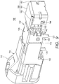
- FIG. 1 is a perspective view illustrating a state where a connector of an embodiment of the present invention is mounted on a substrate.
- FIG. 2 is a front view of the connector.
- FIG. 3 is a rear view of the connector.
- FIG. 4 is a bottom view of the connector.
- FIG. 5 is a right side view of the connector.
- FIG. 6 is a left side view of the connector.
- front end (front) side the side of an end of the connector at which the connector is connected to a mating connector
- rear end the other end opposite to the front end
- bottom surface the surface facing the mounting surface
- Connector 100 of the present embodiment is, but not limited to, a connector for data transfer which is used for high-speed data transfer between apparatuses.
- Connector 100 of the present embodiment is applicable to any connectors which are mounted on an end portion of a substrate.
- Connector 100 of the present embodiment illustrated in FIG. 1 includes connector main body 102 that is mounted on mounting surface 21 of an end portion of substrate 20 (see FIGS. 4 and 5 ), and interface part (connecting part) 104 that projects from connector main body 102 and is fitted and connected with a mating connector (see FIGS. 4 and 5 ).
- connector 100 has a shape provided with cutout part 103 that is provided by cutting out the bottom surface side of connector main body 102.
- Connector main body 102 is attached on an end portion of a substrate positioned at cutout part 103. In this manner, connector 100 is mounted on substrate 20 in the state where interface part 104 protrudes from end surface 22 of substrate 20.
- interface part 104 When interface part 104 is fitted with the interface part of a mating connector connected with another cable or another substrate, interface part 104 is electrically connected with the mating connector. Interface part 104 is disposed such that interface part 104 protrudes from end surface 22 of substrate 20.
- interface part 104 includes first fitting part 112 having first opening part 112a that opens to the front side (front end side), and second fitting part 114 having second opening part 114a. That is, connector 100 of the present embodiment is electrically connected at the two different parts, first and second fitting parts 112 and 114, with the corresponding parts of the interface part of the mating connector.
- First fitting part 112 and second fitting part 114 are disposed side by side in the lateral direction of connector 100 (the direction that is parallel to mounting surface 21 and extends along end surface 22, or the width direction of connector 100).
- interface part 104 has an asymmetric shape in the width direction of interface part 104
- connector 100 has a bilaterally asymmetric shape in its entirety.
- first opening part 112a and second opening part 114a open to the outside and are adjacent to each other, with outer housing 110.
- first opening part 112a On the inner periphery surface of first opening part 112a which extends along the direction in which the connector is connected with the mating connector, a key groove corresponding to the fitting shape of the mating connector to be connected is formed. Since first fitting part 112 has an inner periphery surface having a shape corresponding to the fitted part of the mating connector to be connected, only mating connectors that have a fitted part having a predetermined shape is allowed to be fitted with first fitting part 112.
- First fitting part 112 includes outer housing 110, cylindrical part 122 covered by outer housing 110, and first terminal 130 disposed in cylindrical part 122 and configured to be connected with a mating connector terminal.
- FIG. 7 is a sectional view taken along line II-II of FIG. 2 .
- cylindrical part 122 is integrally connected with an end portion, which is covered by outer housing 110, of shell 120.
- cylindrical part 122 is disposed in first opening part 112a of outer housing 110 such that it faces the front side (front end side).
- Cylindrical part 122 and shell 120 integrally provided with cylindrical part 122 are composed of a plate member having conductivity, and in this case, cylindrical part 122 and shell 120 are configured by processing a sheet metal.
- Shell 120 has a box-like shape that opens to the bottom surface side, and covers inner housing 140 on which first terminal 130 is fixed. Shell 120 is connected at a front side wall part with cylindrical part 122 such that the inner spaces thereof are continuously provided. It is to be noted that, together with weight part 180 and inner housing 140, shell 120 is provided as a principal part of connector main body 102. As illustrated in FIG. 4 , at the lower end of shell 120, four leg parts 121 protruding downward are formed with predetermined spaces therebetween. Leg parts 121 are disposed to surround rear end portion 132 of first terminal 130 disposed in first opening part 112a (see FIG. 2 ). Leg parts 121 are inserted to respective through holes 224 (see FIG. 11 ) formed in substrate 20, and are fixed to be grounded through solder.
- Inner housing 140 is formed of a material having an insulation property, and in this case, inner housing 140 is formed of a resin. As illustrated in FIGS. 4 , 5 and 7 , rear end portion (connecting end) 132 of first terminal 130 that is connected to substrate 20 protrudes downward from the bottom surface of inner housing 140. Rear end portion 132 of first terminal 130 that protrudes from the bottom surface of inner housing 140 is inserted to corresponding through hole 221 (see FIG. 11 ) formed in substrate 20 and is joined by soldering.
- connector 100 includes second terminal 150 in addition to first terminal 130, and second terminal 150 is disposed in second opening part 114a.
- FIG. 8 is a sectional view taken along line III-III of FIG. 2 .
- second terminal 150 is disposed such that its front end portion serving as the contacting part extends along the fitting direction in second opening part 114a of second fitting part 114.
- the front end portion of second terminal 150 is disposed parallel to first terminal 130 (end portion) in first opening part 112a.
- rear end portion 152 of second terminal 150 is disposed to protrude to the bottom surface side as with rear end portion 132 of first terminal 130.
- Rear end portion 152 is inserted to corresponding through hole 222 (see FIG. 11 ) formed in substrate 20 and is joined by soldering.
- connector 100 relative to substrate 20 is set by inserting rear end portion 132 of first terminal 130 to through hole 221, rear end portion 152 of second terminal 150 to through hole 222, and leg parts 121 to through holes 224.
- FIG. 9 illustrates weight part 180 of connector 100.
- weight part 180 is formed by processing a sheet metal as with shell 120.
- Weight part 180 is formed by bending a sheet metal to cover the top surface and lateral surfaces of the rear end portion of shell 120 in an inverted U-shape with the top surface 181 and lateral surfaces 182 and 183 in back view.
- Weight part 180 includes hooks 184 on lateral surfaces 182 and 183 that engage the lateral surfaces of shell 120.
- weight part 180 In weight part 180, top surface 181 and lateral surfaces 182 and 183 are fitted on shell 120, thus restricting the movement in the lateral direction (the width direction of the connector) with respect to shell 120, that is, the direction that is orthogonal to the direction in which the connector is connected with the mating connector, and is parallel to mounting surface 21 of substrate 20.
- the engagement of hooks 184 and shell 120 restricts the vertical movement of weight part 180 with respect to shell 120.
- weight part 180 may be formed by using a sheet metal having the thickness same as that of the sheet metal used as shell 120.
- the position of gravity center G of connector 100 can be set at a position on the rear end side of connector 100 by only processing a sheet metal by bending. That is, it is not necessary to separately manufacture an expensive metal mold to manufacture a die casting, and noise tolerance can be readily achieved by processing an inexpensive sheet metal. Moreover, increase in lifetime of the metal mold itself with use of a press member is achieved, and the connector 100 can be held at an end portion of substrate 20 with gravity center G being stabilized, while achieving cost reduction.
- connector 100 having the above-mentioned configuration includes on its bottom surface (attachment surface) 105 leg part 170 (171 to 174) that protrudes downward. It is to be noted that, in FIG. 4 , leg part 170 (171 to 174) is hatched for convenience.
- Leg part 170 includes front end leg parts 171 and 172 (first leg parts 171 and second leg parts 172) and rear end side leg parts (third leg parts) 173 and 174 which are provided at respective positions on bottom surface 105 of connector main body 102 that faces mounting surface 21 when connector 100 is mounted on substrate 20.
- Front end side leg parts 171 and 172 and rear end side leg parts 173 and 174 are provided. Front end side leg parts 171 and 172 and rear end side leg parts 173 and 174 define a gap between bottom surface 105 and mounting surface 21. Front end side leg parts 171 and 172 are provided on bottom surface 105 at respective position nearer to end surface 22 of substrate 20 relative to rear end side leg parts 173 and 174. It is to be noted that one or both of the two parts, rear end side leg parts 173 and 174, is used as a third leg part.
- FIG. 10 is a bottom view illustrating a positional relationship between the leg parts and the gravity center of the connector on the substrate
- FIG. 11 is a side view illustrating a positional relationship between the leg parts and the gravity center of the connector on the substrate.
- Front end side leg parts 171 and 172 are provided with a space therebetween along the lateral direction of the connector, that is, the direction that is orthogonal to the connecting direction of interface part 104, and extends along mounting surface 21 of substrate 20. Front end side leg parts 171 and 172 are disposed with a space therebetween along end surface 22 at respective positions near end surface 22. It is to be noted that in bottom view, the center between front end side leg parts 171 and 172 is adjacent to the end surface 22, with a space therebetween. In this manner, the position of the gravity center of connector 100 itself can be further separated from end surface 22 of substrate 20.
- rear end side leg parts 173 and 174 are located at respective positions on the inner side of substrate 20, that is, on the rear end portion side of connector 100 relative to front end side leg parts 171 and 172.
- leg parts 171 to 174 are set such that gravity center G of connector 100 is located in triangular regions E1 and E2 defined by straight lines that connect front end side leg parts 171 and 172 and rear end side leg parts 173 or 174.
- leg parts 171 to 174 are provided on bottom surface 105 such that gravity center G is located in triangular regions E1 and E2 which are defined by connecting the centers of leg parts 171 to 174 in bottom view (centers on which load of connector 100 is exerted) by straight lines (or, the region obtained by connecting the centers of leg parts 171, 172 and 173, and the region obtained by connecting the centers of leg parts 171, 172 and 174).
- gravity center G of connector 100 is located in one or both of triangular region E1 of front end side leg parts 171 and 172 and rear end side leg parts 173, and triangular region E2 of front end side leg parts 171 and 172 and rear end side leg parts 174.
- the protrusion length L1 of front end side leg parts 171 and 172 from the bottom surface (bottom surface 105 of connector main body 102) of connector 100 is preferably equal to or greater than protrusion length L2 of rear end side leg parts 173 and 174 from the bottom surface of connector 100.
- L1>L2 is satisfied.
- Lengths L1 and L2 of leg parts 171 to 174 may be increased on the front end side and reduced on the rear end side by a tolerance from a predetermined length (height of substrate 20) n, for example.
- Front end side leg parts 171 and 172 are each set to n+0.05 mm
- rear end side leg parts 173 and 174 are each set to n-0.05 mm or the like.
- connector main body 102 of connector 100 is integrally provided with weight part 180 that is fitted with shell 120.
- connector 100 having the above-mentioned configuration, when connector 100 is mounted to substrate 20 by pin-in-paste, first, solder paste is thinly applied to a circuit pattern on mounting surface 21 of substrate 20 with use of masking, and then connector 100 is disposed at a corresponding position. At this time, connector 100 is placed perpendicular to substrate 20, and disposed at a corresponding position.
- gravity center G of connector 100 is located between front end side leg parts 171 and 172, and rear end side leg parts 173 and 174 (or one of rear end side leg parts 173 and 174) (in region E1 or E2 illustrated in FIG. 11 ).
- connector 100 can be stably held on mounting surface 21 in the state where interface part 104 projects from end surface 22 of substrate 20.
- the height of front end side leg parts 171 and 172 is greater than that of rear end side leg parts 173 and 174 (one of which may not be provided) (L1>L2).
- gravity center G of connector 100 can be positioned on the rear end portion side of the connector relative to front end side leg parts 171 and 172 in the region of substrate 20.
- gravity center G of connector 100 is located on the rear end side of connector 100 relative to front end side leg parts 171 and 172.
- gravity center G is located in regions E1 and E2.
- connector 100 when connector 100 is mounted on an end portion of substrate 20, connector 100 can be held such that connector 100 is not moved in front, rear, left and right directions, and substrate 20 itself provided with connector 100 can be downsized.
- front end side leg parts 171 and 172 of leg part 170 are formed on the bottom surface of inner housing 140 along the end sides separated in the width direction in the present embodiment, this is not limitative, and front end side leg parts 171 and 172 may be provided at an end portion on the end side on the bottom surface of shell 120.
- rear end side leg parts 173 and 174 are provided at an end portion on the rear end side on the bottom surface of shell 120, rear end side leg parts 173 and 174 may be formed along the end portion on the rear end side on the bottom surface of shell 120, and along the end sides separated in the width direction on the bottom surface of inner housing 140.
- the connector according to claim 1 is suitable for a connector that is mounted on a substrate of an electronic component to be downsized.
Landscapes
- Coupling Device And Connection With Printed Circuit (AREA)
Claims (6)
- Connecteur (100), comprenant :un corps principal de connecteur (102) incluant une surface de fixation (105) configurée pour faire face à une surface de montage (21) d'un substrat (20), le corps principal de connecteur (102) étant configuré pour être monté sur la surface de montage (21) ;une pièce de connexion (104) prévue pour faire saillie à partir du corps principal de connecteur, et pour dépasser à partir d'une surface d'extrémité (22) de la surface de montage (21), la pièce de connexion (104) étant configurée pour être connectée à un connecteur homologue ;des pièces formant pattes (121) introduites dans des trous débouchants respectifs (224) formés dans le substrat (20), etdes extrémités de connexion (132, 152), lesquelles sont connectées par voie électrique au substrat (20) ;caractérisé en ce quedes première (171), deuxième (172), et troisième (173 ou 174) pièces formant pattes sont prévues pour faire saillie à partir de la surface de fixation (105), les première, deuxième et troisième pièces formant pattes (171, 172, 173, 174) étant configurées pour abouter sur la surface de montage (21) du substrat (20) et définir un entrebâillement (L1, L2) entre la surface de fixation (105) et ladite surface de montage (21),dans lequel la première pièce formant patte (171) et la deuxième pièce formant patte (172) sont prévues sur la surface de fixation (105) sur le côté de surface d'extrémité (22) du substrat (20) par rapport aux troisièmes pièces formant pattes (173 ou 174), dans lequel une pièce formant poids (180) est prévue sur la portion d'extrémité arrière du corps principal de connecteur (102), et les première (171), deuxième (172), et troisième (173 ou 174) pièces formant pattes sont prévues sur la surface de fixation (105) de telle sorte qu'un centre de gravité (G) du connecteur (100) même se trouve dans les régions du triangle défini en reliant les centres des première (171), deuxième (172), et troisième (173 ou 174) pièces formant pattes,dans lequel le connecteur (100) est doté d'une pièce de découpe (103) en découpant l'entièreté du corps principal de connecteur (102) sur le côté de surface de fixation (105), de sorte que la pièce de connexion (104) fait saillie à partir de la surface d'extrémité (22) du substrat (20), et que la première pièce formant patte (171) et la deuxième pièce formant patte (172) sont chacune prévues de manière à abouter sur la pièce de connexion (104).
- Connecteur selon la revendication 1, dans lequel une longueur saillante (L1) de chacune des première (171) et deuxième (172) pièces formant pattes est supérieure à une longueur saillante (L2) de chacune des troisièmes pièces formant pattes (173, 174).
- Connecteur selon la revendication 1 ou 2, dans lequel la pièce de connexion (104) présente une forme qui est asymétrique dans une direction de largeur.
- Connecteur selon l'une quelconque des revendications 1 à 3, dans lequel la pièce formant poids (180) est configurée pour ajuster le centre de gravité.
- Connecteur selon la revendication 4, dans lequel la pièce formant poids est formée d'une tôle.
- Connecteur selon l'une quelconque des revendications 1 à 5, configuré de telle sorte qu'une longueur (L3) allant de la surface d'extrémité (22) du substrat (20) à une portion d'extrémité avant, laquelle est une portion d'extrémité de la pièce de connexion (104) dans une direction saillante de la pièce de connexion, est supérieure ou égale à une longueur (L4) allant de la surface d'extrémité (22) du substrat à une portion d'extrémité arrière du corps principal de connecteur (102).
Applications Claiming Priority (1)
| Application Number | Priority Date | Filing Date | Title |
|---|---|---|---|
| JP2014122688A JP6398354B2 (ja) | 2014-06-13 | 2014-06-13 | コネクタ |
Publications (2)
| Publication Number | Publication Date |
|---|---|
| EP2955791A1 EP2955791A1 (fr) | 2015-12-16 |
| EP2955791B1 true EP2955791B1 (fr) | 2018-05-23 |
Family
ID=53385550
Family Applications (1)
| Application Number | Title | Priority Date | Filing Date |
|---|---|---|---|
| EP15171634.7A Active EP2955791B1 (fr) | 2014-06-13 | 2015-06-11 | Connecteur pour être monté sur le bord d'un pcb, ayant une arrière partie métallique, qui corrige le centre de masse |
Country Status (3)
| Country | Link |
|---|---|
| EP (1) | EP2955791B1 (fr) |
| JP (1) | JP6398354B2 (fr) |
| CN (1) | CN105322391B (fr) |
Cited By (2)
| Publication number | Priority date | Publication date | Assignee | Title |
|---|---|---|---|---|
| US20220069492A1 (en) * | 2018-12-17 | 2022-03-03 | Amphenol Tuchel Industrial GmbH | Multi-part printed circuit board adapter plug |
| EP3857648B1 (fr) * | 2018-09-28 | 2024-03-13 | Unify Patente GmbH & Co. KG | Système de connecteurs électriques |
Families Citing this family (3)
| Publication number | Priority date | Publication date | Assignee | Title |
|---|---|---|---|---|
| DE102017104819A1 (de) * | 2017-03-08 | 2018-09-13 | Phoenix Contact Gmbh & Co. Kg | Bauelement, Bestückungshilfe und Verfahren zur Lötbefestigung des Bauelements |
| JP6852894B2 (ja) * | 2017-06-14 | 2021-03-31 | 日本圧着端子製造株式会社 | コネクタ |
| BE1025487B1 (de) * | 2017-08-21 | 2019-03-27 | Phoenix Contact Gmbh & Co. Kg | Elektrischer steckverbinder zur ausbildung eines leiterplattensteckverbinders an einer leiterplatte |
Citations (1)
| Publication number | Priority date | Publication date | Assignee | Title |
|---|---|---|---|---|
| EP0627791A1 (fr) * | 1993-06-04 | 1994-12-07 | Framatome Connectors International | Ensemble de connexion pour cartes de circuits imprimés |
Family Cites Families (15)
| Publication number | Priority date | Publication date | Assignee | Title |
|---|---|---|---|---|
| JP2753190B2 (ja) * | 1993-09-20 | 1998-05-18 | 富士通株式会社 | 表面実装型コネクタ |
| JP2000251986A (ja) * | 1999-02-25 | 2000-09-14 | D D K Ltd | 電気コネクタ |
| WO2006035767A1 (fr) * | 2004-09-29 | 2006-04-06 | Autonetworks Technologies, Ltd. | Connecteur pour substrat |
| CN2821934Y (zh) * | 2005-09-30 | 2006-09-27 | 华为技术有限公司 | 连接器 |
| JP5221188B2 (ja) * | 2008-04-07 | 2013-06-26 | 矢崎総業株式会社 | シールドコネクタ |
| CN102280732B (zh) * | 2010-06-10 | 2014-01-29 | 上海莫仕连接器有限公司 | 电连接器 |
| JP5550528B2 (ja) * | 2010-11-05 | 2014-07-16 | タイコエレクトロニクスジャパン合同会社 | 回路基板組立体、コネクタ、はんだ付け方法 |
| FR2969400B1 (fr) * | 2010-12-16 | 2013-08-30 | Radiall Sa | Connecteur pour carte de circuit imprime |
| JP5747653B2 (ja) * | 2011-05-20 | 2015-07-15 | ミツミ電機株式会社 | 電気コネクタ |
| US8430675B2 (en) * | 2011-06-24 | 2013-04-30 | Tyco Electronics Corporation | Edge mount electrical connector |
| CN202111336U (zh) * | 2011-07-04 | 2012-01-11 | 莫列斯公司 | 电连接装置 |
| JP5741335B2 (ja) * | 2011-09-10 | 2015-07-01 | 住友電装株式会社 | 基板用コネクタ |
| JP5259858B1 (ja) * | 2012-05-16 | 2013-08-07 | 株式会社東芝 | コネクタ、回路モジュールおよび電子機器 |
| JP6092609B2 (ja) * | 2012-12-19 | 2017-03-08 | 矢崎総業株式会社 | ダストキャップおよびコネクタ係合体 |
| CN103825128B (zh) * | 2014-03-21 | 2015-11-25 | 衢州赋腾信息科技有限公司 | 网线连接器 |
-
2014
- 2014-06-13 JP JP2014122688A patent/JP6398354B2/ja active Active
-
2015
- 2015-06-08 CN CN201510310143.7A patent/CN105322391B/zh active Active
- 2015-06-11 EP EP15171634.7A patent/EP2955791B1/fr active Active
Patent Citations (1)
| Publication number | Priority date | Publication date | Assignee | Title |
|---|---|---|---|---|
| EP0627791A1 (fr) * | 1993-06-04 | 1994-12-07 | Framatome Connectors International | Ensemble de connexion pour cartes de circuits imprimés |
Cited By (3)
| Publication number | Priority date | Publication date | Assignee | Title |
|---|---|---|---|---|
| EP3857648B1 (fr) * | 2018-09-28 | 2024-03-13 | Unify Patente GmbH & Co. KG | Système de connecteurs électriques |
| US20220069492A1 (en) * | 2018-12-17 | 2022-03-03 | Amphenol Tuchel Industrial GmbH | Multi-part printed circuit board adapter plug |
| US11881645B2 (en) * | 2018-12-17 | 2024-01-23 | Amphenol Tuchel Industrial GmbH | Multi-part printed circuit board adapter plug |
Also Published As
| Publication number | Publication date |
|---|---|
| CN105322391B (zh) | 2020-05-05 |
| EP2955791A1 (fr) | 2015-12-16 |
| JP2016004626A (ja) | 2016-01-12 |
| CN105322391A (zh) | 2016-02-10 |
| JP6398354B2 (ja) | 2018-10-03 |
Similar Documents
| Publication | Publication Date | Title |
|---|---|---|
| JP6663565B2 (ja) | 基板用コネクタ | |
| EP2955791B1 (fr) | Connecteur pour être monté sur le bord d'un pcb, ayant une arrière partie métallique, qui corrige le centre de masse | |
| US9039428B2 (en) | Board-to-board connector | |
| TWI509910B (zh) | 連接器 | |
| JP2022103329A (ja) | コネクタ | |
| JP4494441B2 (ja) | 電気コネクタ | |
| EP1988608A1 (fr) | Connecteur | |
| WO2018221095A1 (fr) | Connecteur électrique | |
| JP6686145B2 (ja) | コンタクト | |
| JP6006356B2 (ja) | コンタクト及び該コンタクトを使用するコネクタ | |
| US9979122B1 (en) | Electronic device and connector | |
| TWI668924B (zh) | 連接器 | |
| JP2010113848A (ja) | 基板用コネクタ | |
| US8888505B2 (en) | Board-to-board connector | |
| JP2011258508A (ja) | コネクタ | |
| US9004944B2 (en) | Connector having an armature for fastening the connector to a printed circuit board | |
| JP2007257999A (ja) | 回路基板用電気コネクタ | |
| EP2613410A1 (fr) | Structure pour empêcher l'insertion inappropriée d'un connecteur | |
| EP3051634B1 (fr) | Connecteur | |
| JP2013182808A (ja) | シールドカバーおよび当該シールドカバーで覆われるコネクタ | |
| JP2016184505A (ja) | 基板接続用電気コネクタ及び基板接続用電気コネクタ装置 | |
| CN110800166B (zh) | 基板用连接器及电路基板和基板用连接器的连接结构 | |
| CN111384608B (zh) | 基板用连接器 | |
| JP6350072B2 (ja) | 電気コネクタ | |
| JP2010080893A (ja) | 回路モジュール |
Legal Events
| Date | Code | Title | Description |
|---|---|---|---|
| PUAI | Public reference made under article 153(3) epc to a published international application that has entered the european phase |
Free format text: ORIGINAL CODE: 0009012 |
|
| AK | Designated contracting states |
Kind code of ref document: A1 Designated state(s): AL AT BE BG CH CY CZ DE DK EE ES FI FR GB GR HR HU IE IS IT LI LT LU LV MC MK MT NL NO PL PT RO RS SE SI SK SM TR |
|
| AX | Request for extension of the european patent |
Extension state: BA ME |
|
| 17P | Request for examination filed |
Effective date: 20160616 |
|
| RBV | Designated contracting states (corrected) |
Designated state(s): AL AT BE BG CH CY CZ DE DK EE ES FI FR GB GR HR HU IE IS IT LI LT LU LV MC MK MT NL NO PL PT RO RS SE SI SK SM TR |
|
| 17Q | First examination report despatched |
Effective date: 20170602 |
|
| GRAP | Despatch of communication of intention to grant a patent |
Free format text: ORIGINAL CODE: EPIDOSNIGR1 |
|
| RIC1 | Information provided on ipc code assigned before grant |
Ipc: H01R 13/506 20060101ALN20171108BHEP Ipc: H01R 13/6594 20110101ALI20171108BHEP Ipc: H01R 12/75 20110101ALN20171108BHEP Ipc: H01R 24/50 20110101ALN20171108BHEP Ipc: H01R 12/72 20110101AFI20171108BHEP |
|
| INTG | Intention to grant announced |
Effective date: 20171213 |
|
| RIC1 | Information provided on ipc code assigned before grant |
Ipc: H01R 12/72 20110101AFI20171204BHEP Ipc: H01R 24/50 20110101ALN20171204BHEP Ipc: H01R 13/6594 20110101ALI20171204BHEP Ipc: H01R 12/75 20110101ALN20171204BHEP Ipc: H01R 13/506 20060101ALN20171204BHEP |
|
| GRAS | Grant fee paid |
Free format text: ORIGINAL CODE: EPIDOSNIGR3 |
|
| GRAA | (expected) grant |
Free format text: ORIGINAL CODE: 0009210 |
|
| AK | Designated contracting states |
Kind code of ref document: B1 Designated state(s): AL AT BE BG CH CY CZ DE DK EE ES FI FR GB GR HR HU IE IS IT LI LT LU LV MC MK MT NL NO PL PT RO RS SE SI SK SM TR |
|
| REG | Reference to a national code |
Ref country code: GB Ref legal event code: FG4D |
|
| REG | Reference to a national code |
Ref country code: CH Ref legal event code: EP |
|
| REG | Reference to a national code |
Ref country code: IE Ref legal event code: FG4D |
|
| REG | Reference to a national code |
Ref country code: AT Ref legal event code: REF Ref document number: 1002255 Country of ref document: AT Kind code of ref document: T Effective date: 20180615 |
|
| REG | Reference to a national code |
Ref country code: DE Ref legal event code: R096 Ref document number: 602015011349 Country of ref document: DE |
|
| REG | Reference to a national code |
Ref country code: FR Ref legal event code: PLFP Year of fee payment: 4 |
|
| REG | Reference to a national code |
Ref country code: NL Ref legal event code: MP Effective date: 20180523 |
|
| REG | Reference to a national code |
Ref country code: LT Ref legal event code: MG4D |
|
| PG25 | Lapsed in a contracting state [announced via postgrant information from national office to epo] |
Ref country code: ES Free format text: LAPSE BECAUSE OF FAILURE TO SUBMIT A TRANSLATION OF THE DESCRIPTION OR TO PAY THE FEE WITHIN THE PRESCRIBED TIME-LIMIT Effective date: 20180523 Ref country code: BG Free format text: LAPSE BECAUSE OF FAILURE TO SUBMIT A TRANSLATION OF THE DESCRIPTION OR TO PAY THE FEE WITHIN THE PRESCRIBED TIME-LIMIT Effective date: 20180823 Ref country code: FI Free format text: LAPSE BECAUSE OF FAILURE TO SUBMIT A TRANSLATION OF THE DESCRIPTION OR TO PAY THE FEE WITHIN THE PRESCRIBED TIME-LIMIT Effective date: 20180523 Ref country code: LT Free format text: LAPSE BECAUSE OF FAILURE TO SUBMIT A TRANSLATION OF THE DESCRIPTION OR TO PAY THE FEE WITHIN THE PRESCRIBED TIME-LIMIT Effective date: 20180523 Ref country code: SE Free format text: LAPSE BECAUSE OF FAILURE TO SUBMIT A TRANSLATION OF THE DESCRIPTION OR TO PAY THE FEE WITHIN THE PRESCRIBED TIME-LIMIT Effective date: 20180523 Ref country code: NO Free format text: LAPSE BECAUSE OF FAILURE TO SUBMIT A TRANSLATION OF THE DESCRIPTION OR TO PAY THE FEE WITHIN THE PRESCRIBED TIME-LIMIT Effective date: 20180823 |
|
| PG25 | Lapsed in a contracting state [announced via postgrant information from national office to epo] |
Ref country code: RS Free format text: LAPSE BECAUSE OF FAILURE TO SUBMIT A TRANSLATION OF THE DESCRIPTION OR TO PAY THE FEE WITHIN THE PRESCRIBED TIME-LIMIT Effective date: 20180523 Ref country code: LV Free format text: LAPSE BECAUSE OF FAILURE TO SUBMIT A TRANSLATION OF THE DESCRIPTION OR TO PAY THE FEE WITHIN THE PRESCRIBED TIME-LIMIT Effective date: 20180523 Ref country code: HR Free format text: LAPSE BECAUSE OF FAILURE TO SUBMIT A TRANSLATION OF THE DESCRIPTION OR TO PAY THE FEE WITHIN THE PRESCRIBED TIME-LIMIT Effective date: 20180523 Ref country code: GR Free format text: LAPSE BECAUSE OF FAILURE TO SUBMIT A TRANSLATION OF THE DESCRIPTION OR TO PAY THE FEE WITHIN THE PRESCRIBED TIME-LIMIT Effective date: 20180824 Ref country code: NL Free format text: LAPSE BECAUSE OF FAILURE TO SUBMIT A TRANSLATION OF THE DESCRIPTION OR TO PAY THE FEE WITHIN THE PRESCRIBED TIME-LIMIT Effective date: 20180523 |
|
| REG | Reference to a national code |
Ref country code: AT Ref legal event code: MK05 Ref document number: 1002255 Country of ref document: AT Kind code of ref document: T Effective date: 20180523 |
|
| PG25 | Lapsed in a contracting state [announced via postgrant information from national office to epo] |
Ref country code: RO Free format text: LAPSE BECAUSE OF FAILURE TO SUBMIT A TRANSLATION OF THE DESCRIPTION OR TO PAY THE FEE WITHIN THE PRESCRIBED TIME-LIMIT Effective date: 20180523 Ref country code: CZ Free format text: LAPSE BECAUSE OF FAILURE TO SUBMIT A TRANSLATION OF THE DESCRIPTION OR TO PAY THE FEE WITHIN THE PRESCRIBED TIME-LIMIT Effective date: 20180523 Ref country code: SK Free format text: LAPSE BECAUSE OF FAILURE TO SUBMIT A TRANSLATION OF THE DESCRIPTION OR TO PAY THE FEE WITHIN THE PRESCRIBED TIME-LIMIT Effective date: 20180523 Ref country code: PL Free format text: LAPSE BECAUSE OF FAILURE TO SUBMIT A TRANSLATION OF THE DESCRIPTION OR TO PAY THE FEE WITHIN THE PRESCRIBED TIME-LIMIT Effective date: 20180523 Ref country code: AT Free format text: LAPSE BECAUSE OF FAILURE TO SUBMIT A TRANSLATION OF THE DESCRIPTION OR TO PAY THE FEE WITHIN THE PRESCRIBED TIME-LIMIT Effective date: 20180523 Ref country code: EE Free format text: LAPSE BECAUSE OF FAILURE TO SUBMIT A TRANSLATION OF THE DESCRIPTION OR TO PAY THE FEE WITHIN THE PRESCRIBED TIME-LIMIT Effective date: 20180523 Ref country code: DK Free format text: LAPSE BECAUSE OF FAILURE TO SUBMIT A TRANSLATION OF THE DESCRIPTION OR TO PAY THE FEE WITHIN THE PRESCRIBED TIME-LIMIT Effective date: 20180523 |
|
| REG | Reference to a national code |
Ref country code: CH Ref legal event code: PL |
|
| REG | Reference to a national code |
Ref country code: DE Ref legal event code: R097 Ref document number: 602015011349 Country of ref document: DE |
|
| PG25 | Lapsed in a contracting state [announced via postgrant information from national office to epo] |
Ref country code: SM Free format text: LAPSE BECAUSE OF FAILURE TO SUBMIT A TRANSLATION OF THE DESCRIPTION OR TO PAY THE FEE WITHIN THE PRESCRIBED TIME-LIMIT Effective date: 20180523 Ref country code: IT Free format text: LAPSE BECAUSE OF FAILURE TO SUBMIT A TRANSLATION OF THE DESCRIPTION OR TO PAY THE FEE WITHIN THE PRESCRIBED TIME-LIMIT Effective date: 20180523 |
|
| REG | Reference to a national code |
Ref country code: BE Ref legal event code: MM Effective date: 20180630 |
|
| REG | Reference to a national code |
Ref country code: IE Ref legal event code: MM4A |
|
| PG25 | Lapsed in a contracting state [announced via postgrant information from national office to epo] |
Ref country code: LU Free format text: LAPSE BECAUSE OF NON-PAYMENT OF DUE FEES Effective date: 20180611 Ref country code: MC Free format text: LAPSE BECAUSE OF FAILURE TO SUBMIT A TRANSLATION OF THE DESCRIPTION OR TO PAY THE FEE WITHIN THE PRESCRIBED TIME-LIMIT Effective date: 20180523 |
|
| PLBE | No opposition filed within time limit |
Free format text: ORIGINAL CODE: 0009261 |
|
| STAA | Information on the status of an ep patent application or granted ep patent |
Free format text: STATUS: NO OPPOSITION FILED WITHIN TIME LIMIT |
|
| PG25 | Lapsed in a contracting state [announced via postgrant information from national office to epo] |
Ref country code: CH Free format text: LAPSE BECAUSE OF NON-PAYMENT OF DUE FEES Effective date: 20180630 Ref country code: IE Free format text: LAPSE BECAUSE OF NON-PAYMENT OF DUE FEES Effective date: 20180611 Ref country code: LI Free format text: LAPSE BECAUSE OF NON-PAYMENT OF DUE FEES Effective date: 20180630 |
|
| 26N | No opposition filed |
Effective date: 20190226 |
|
| PG25 | Lapsed in a contracting state [announced via postgrant information from national office to epo] |
Ref country code: BE Free format text: LAPSE BECAUSE OF NON-PAYMENT OF DUE FEES Effective date: 20180630 Ref country code: SI Free format text: LAPSE BECAUSE OF FAILURE TO SUBMIT A TRANSLATION OF THE DESCRIPTION OR TO PAY THE FEE WITHIN THE PRESCRIBED TIME-LIMIT Effective date: 20180523 |
|
| PG25 | Lapsed in a contracting state [announced via postgrant information from national office to epo] |
Ref country code: AL Free format text: LAPSE BECAUSE OF FAILURE TO SUBMIT A TRANSLATION OF THE DESCRIPTION OR TO PAY THE FEE WITHIN THE PRESCRIBED TIME-LIMIT Effective date: 20180523 |
|
| PG25 | Lapsed in a contracting state [announced via postgrant information from national office to epo] |
Ref country code: MT Free format text: LAPSE BECAUSE OF NON-PAYMENT OF DUE FEES Effective date: 20180611 |
|
| GBPC | Gb: european patent ceased through non-payment of renewal fee |
Effective date: 20190611 |
|
| PG25 | Lapsed in a contracting state [announced via postgrant information from national office to epo] |
Ref country code: TR Free format text: LAPSE BECAUSE OF FAILURE TO SUBMIT A TRANSLATION OF THE DESCRIPTION OR TO PAY THE FEE WITHIN THE PRESCRIBED TIME-LIMIT Effective date: 20180523 |
|
| PG25 | Lapsed in a contracting state [announced via postgrant information from national office to epo] |
Ref country code: GB Free format text: LAPSE BECAUSE OF NON-PAYMENT OF DUE FEES Effective date: 20190611 |
|
| PG25 | Lapsed in a contracting state [announced via postgrant information from national office to epo] |
Ref country code: PT Free format text: LAPSE BECAUSE OF FAILURE TO SUBMIT A TRANSLATION OF THE DESCRIPTION OR TO PAY THE FEE WITHIN THE PRESCRIBED TIME-LIMIT Effective date: 20180523 |
|
| PG25 | Lapsed in a contracting state [announced via postgrant information from national office to epo] |
Ref country code: MK Free format text: LAPSE BECAUSE OF NON-PAYMENT OF DUE FEES Effective date: 20180523 Ref country code: HU Free format text: LAPSE BECAUSE OF FAILURE TO SUBMIT A TRANSLATION OF THE DESCRIPTION OR TO PAY THE FEE WITHIN THE PRESCRIBED TIME-LIMIT; INVALID AB INITIO Effective date: 20150611 Ref country code: CY Free format text: LAPSE BECAUSE OF FAILURE TO SUBMIT A TRANSLATION OF THE DESCRIPTION OR TO PAY THE FEE WITHIN THE PRESCRIBED TIME-LIMIT Effective date: 20180523 |
|
| PG25 | Lapsed in a contracting state [announced via postgrant information from national office to epo] |
Ref country code: IS Free format text: LAPSE BECAUSE OF FAILURE TO SUBMIT A TRANSLATION OF THE DESCRIPTION OR TO PAY THE FEE WITHIN THE PRESCRIBED TIME-LIMIT Effective date: 20180923 |
|
| PGFP | Annual fee paid to national office [announced via postgrant information from national office to epo] |
Ref country code: DE Payment date: 20230620 Year of fee payment: 9 |
|
| PGFP | Annual fee paid to national office [announced via postgrant information from national office to epo] |
Ref country code: FR Payment date: 20240628 Year of fee payment: 10 |