EP2955758A1 - Trench gate mos semiconductor device and method for manufacturing same - Google Patents
Trench gate mos semiconductor device and method for manufacturing same Download PDFInfo
- Publication number
- EP2955758A1 EP2955758A1 EP14833749.6A EP14833749A EP2955758A1 EP 2955758 A1 EP2955758 A1 EP 2955758A1 EP 14833749 A EP14833749 A EP 14833749A EP 2955758 A1 EP2955758 A1 EP 2955758A1
- Authority
- EP
- European Patent Office
- Prior art keywords
- trench
- conductivity
- type
- region
- electrode
- Prior art date
- Legal status (The legal status is an assumption and is not a legal conclusion. Google has not performed a legal analysis and makes no representation as to the accuracy of the status listed.)
- Granted
Links
Images




Classifications
-
- H—ELECTRICITY
- H10—SEMICONDUCTOR DEVICES; ELECTRIC SOLID-STATE DEVICES NOT OTHERWISE PROVIDED FOR
- H10D—INORGANIC ELECTRIC SEMICONDUCTOR DEVICES
- H10D12/00—Bipolar devices controlled by the field effect, e.g. insulated-gate bipolar transistors [IGBT]
- H10D12/411—Insulated-gate bipolar transistors [IGBT]
- H10D12/441—Vertical IGBTs
- H10D12/461—Vertical IGBTs having non-planar surfaces, e.g. having trenches, recesses or pillars in the surfaces of the emitter, base or collector regions
- H10D12/481—Vertical IGBTs having non-planar surfaces, e.g. having trenches, recesses or pillars in the surfaces of the emitter, base or collector regions having gate structures on slanted surfaces, on vertical surfaces, or in grooves, e.g. trench gate IGBTs
-
- H—ELECTRICITY
- H10—SEMICONDUCTOR DEVICES; ELECTRIC SOLID-STATE DEVICES NOT OTHERWISE PROVIDED FOR
- H10D—INORGANIC ELECTRIC SEMICONDUCTOR DEVICES
- H10D12/00—Bipolar devices controlled by the field effect, e.g. insulated-gate bipolar transistors [IGBT]
- H10D12/01—Manufacture or treatment
- H10D12/031—Manufacture or treatment of IGBTs
- H10D12/032—Manufacture or treatment of IGBTs of vertical IGBTs
- H10D12/038—Manufacture or treatment of IGBTs of vertical IGBTs having a recessed gate, e.g. trench-gate IGBTs
-
- H—ELECTRICITY
- H10—SEMICONDUCTOR DEVICES; ELECTRIC SOLID-STATE DEVICES NOT OTHERWISE PROVIDED FOR
- H10D—INORGANIC ELECTRIC SEMICONDUCTOR DEVICES
- H10D62/00—Semiconductor bodies, or regions thereof, of devices having potential barriers
- H10D62/10—Shapes, relative sizes or dispositions of the regions of the semiconductor bodies; Shapes of the semiconductor bodies
- H10D62/102—Constructional design considerations for preventing surface leakage or controlling electric field concentration
- H10D62/103—Constructional design considerations for preventing surface leakage or controlling electric field concentration for increasing or controlling the breakdown voltage of reverse-biased devices
- H10D62/105—Constructional design considerations for preventing surface leakage or controlling electric field concentration for increasing or controlling the breakdown voltage of reverse-biased devices by having particular doping profiles, shapes or arrangements of PN junctions; by having supplementary regions, e.g. junction termination extension [JTE]
- H10D62/106—Constructional design considerations for preventing surface leakage or controlling electric field concentration for increasing or controlling the breakdown voltage of reverse-biased devices by having particular doping profiles, shapes or arrangements of PN junctions; by having supplementary regions, e.g. junction termination extension [JTE] having supplementary regions doped oppositely to or in rectifying contact with regions of the semiconductor bodies, e.g. guard rings with PN or Schottky junctions
-
- H—ELECTRICITY
- H10—SEMICONDUCTOR DEVICES; ELECTRIC SOLID-STATE DEVICES NOT OTHERWISE PROVIDED FOR
- H10D—INORGANIC ELECTRIC SEMICONDUCTOR DEVICES
- H10D62/00—Semiconductor bodies, or regions thereof, of devices having potential barriers
- H10D62/10—Shapes, relative sizes or dispositions of the regions of the semiconductor bodies; Shapes of the semiconductor bodies
- H10D62/13—Semiconductor regions connected to electrodes carrying current to be rectified, amplified or switched, e.g. source or drain regions
- H10D62/133—Emitter regions of BJTs
-
- H—ELECTRICITY
- H10—SEMICONDUCTOR DEVICES; ELECTRIC SOLID-STATE DEVICES NOT OTHERWISE PROVIDED FOR
- H10D—INORGANIC ELECTRIC SEMICONDUCTOR DEVICES
- H10D62/00—Semiconductor bodies, or regions thereof, of devices having potential barriers
- H10D62/10—Shapes, relative sizes or dispositions of the regions of the semiconductor bodies; Shapes of the semiconductor bodies
- H10D62/17—Semiconductor regions connected to electrodes not carrying current to be rectified, amplified or switched, e.g. channel regions
- H10D62/393—Body regions of DMOS transistors or IGBTs
-
- H—ELECTRICITY
- H10—SEMICONDUCTOR DEVICES; ELECTRIC SOLID-STATE DEVICES NOT OTHERWISE PROVIDED FOR
- H10D—INORGANIC ELECTRIC SEMICONDUCTOR DEVICES
- H10D64/00—Electrodes of devices having potential barriers
- H10D64/01—Manufacture or treatment
- H10D64/013—Manufacture or treatment of electrodes having a conductor capacitively coupled to a semiconductor by an insulator
- H10D64/01302—Manufacture or treatment of electrodes having a conductor capacitively coupled to a semiconductor by an insulator the insulator being formed after the semiconductor body, the semiconductor being silicon
- H10D64/01304—Manufacture or treatment of electrodes having a conductor capacitively coupled to a semiconductor by an insulator the insulator being formed after the semiconductor body, the semiconductor being silicon characterised by the conductor
- H10D64/01306—Manufacture or treatment of electrodes having a conductor capacitively coupled to a semiconductor by an insulator the insulator being formed after the semiconductor body, the semiconductor being silicon characterised by the conductor the conductor comprising a layer of silicon contacting the insulator, e.g. polysilicon
-
- H—ELECTRICITY
- H10—SEMICONDUCTOR DEVICES; ELECTRIC SOLID-STATE DEVICES NOT OTHERWISE PROVIDED FOR
- H10D—INORGANIC ELECTRIC SEMICONDUCTOR DEVICES
- H10D64/00—Electrodes of devices having potential barriers
- H10D64/111—Field plates
-
- H—ELECTRICITY
- H10—SEMICONDUCTOR DEVICES; ELECTRIC SOLID-STATE DEVICES NOT OTHERWISE PROVIDED FOR
- H10D—INORGANIC ELECTRIC SEMICONDUCTOR DEVICES
- H10D64/00—Electrodes of devices having potential barriers
- H10D64/111—Field plates
- H10D64/117—Recessed field plates, e.g. trench field plates or buried field plates
-
- H—ELECTRICITY
- H10—SEMICONDUCTOR DEVICES; ELECTRIC SOLID-STATE DEVICES NOT OTHERWISE PROVIDED FOR
- H10D—INORGANIC ELECTRIC SEMICONDUCTOR DEVICES
- H10D64/00—Electrodes of devices having potential barriers
- H10D64/20—Electrodes characterised by their shapes, relative sizes or dispositions
- H10D64/23—Electrodes carrying the current to be rectified, amplified, oscillated or switched, e.g. sources, drains, anodes or cathodes
- H10D64/231—Emitter or collector electrodes for bipolar transistors
-
- H—ELECTRICITY
- H10—SEMICONDUCTOR DEVICES; ELECTRIC SOLID-STATE DEVICES NOT OTHERWISE PROVIDED FOR
- H10D—INORGANIC ELECTRIC SEMICONDUCTOR DEVICES
- H10D64/00—Electrodes of devices having potential barriers
- H10D64/20—Electrodes characterised by their shapes, relative sizes or dispositions
- H10D64/27—Electrodes not carrying the current to be rectified, amplified, oscillated or switched, e.g. gates
- H10D64/311—Gate electrodes for field-effect devices
- H10D64/411—Gate electrodes for field-effect devices for FETs
- H10D64/511—Gate electrodes for field-effect devices for FETs for IGFETs
- H10D64/512—Disposition of the gate electrodes, e.g. buried gates
- H10D64/513—Disposition of the gate electrodes, e.g. buried gates within recesses in the substrate, e.g. trench gates, groove gates or buried gates
-
- H—ELECTRICITY
- H10—SEMICONDUCTOR DEVICES; ELECTRIC SOLID-STATE DEVICES NOT OTHERWISE PROVIDED FOR
- H10D—INORGANIC ELECTRIC SEMICONDUCTOR DEVICES
- H10D64/00—Electrodes of devices having potential barriers
- H10D64/60—Electrodes characterised by their materials
- H10D64/66—Electrodes having a conductor capacitively coupled to a semiconductor by an insulator, e.g. MIS electrodes
- H10D64/661—Electrodes having a conductor capacitively coupled to a semiconductor by an insulator, e.g. MIS electrodes the conductor comprising a layer of silicon contacting the insulator, e.g. polysilicon having vertical doping variation
-
- H—ELECTRICITY
- H10—SEMICONDUCTOR DEVICES; ELECTRIC SOLID-STATE DEVICES NOT OTHERWISE PROVIDED FOR
- H10P—GENERIC PROCESSES OR APPARATUS FOR THE MANUFACTURE OR TREATMENT OF DEVICES COVERED BY CLASS H10
- H10P14/00—Formation of materials, e.g. in the shape of layers or pillars
- H10P14/60—Formation of materials, e.g. in the shape of layers or pillars of insulating materials
- H10P14/63—Formation of materials, e.g. in the shape of layers or pillars of insulating materials characterised by the formation processes
- H10P14/6326—Deposition processes
- H10P14/6328—Deposition from the gas or vapour phase
- H10P14/6334—Deposition from the gas or vapour phase using decomposition or reaction of gaseous or vapour phase compounds, i.e. chemical vapour deposition
-
- H—ELECTRICITY
- H10—SEMICONDUCTOR DEVICES; ELECTRIC SOLID-STATE DEVICES NOT OTHERWISE PROVIDED FOR
- H10P—GENERIC PROCESSES OR APPARATUS FOR THE MANUFACTURE OR TREATMENT OF DEVICES COVERED BY CLASS H10
- H10P14/00—Formation of materials, e.g. in the shape of layers or pillars
- H10P14/60—Formation of materials, e.g. in the shape of layers or pillars of insulating materials
- H10P14/66—Formation of materials, e.g. in the shape of layers or pillars of insulating materials characterised by the type of materials
- H10P14/668—Formation of materials, e.g. in the shape of layers or pillars of insulating materials characterised by the type of materials the materials being characterised by the deposition precursor materials
- H10P14/6681—Formation of materials, e.g. in the shape of layers or pillars of insulating materials characterised by the type of materials the materials being characterised by the deposition precursor materials the precursor containing a compound comprising Si
- H10P14/6682—Formation of materials, e.g. in the shape of layers or pillars of insulating materials characterised by the type of materials the materials being characterised by the deposition precursor materials the precursor containing a compound comprising Si the compound being a silane, e.g. disilane, methylsilane or chlorosilane
-
- H—ELECTRICITY
- H10—SEMICONDUCTOR DEVICES; ELECTRIC SOLID-STATE DEVICES NOT OTHERWISE PROVIDED FOR
- H10P—GENERIC PROCESSES OR APPARATUS FOR THE MANUFACTURE OR TREATMENT OF DEVICES COVERED BY CLASS H10
- H10P14/00—Formation of materials, e.g. in the shape of layers or pillars
- H10P14/60—Formation of materials, e.g. in the shape of layers or pillars of insulating materials
- H10P14/69—Inorganic materials
- H10P14/692—Inorganic materials composed of oxides, glassy oxides or oxide-based glasses
- H10P14/6921—Inorganic materials composed of oxides, glassy oxides or oxide-based glasses containing silicon
- H10P14/69215—Inorganic materials composed of oxides, glassy oxides or oxide-based glasses containing silicon the material being a silicon oxide, e.g. SiO2
Definitions
- the present invention relates to a trench gate MOS semiconductor device that is used in, for example, a power conversion apparatus and a method for manufacturing the same, and more particularly, to an insulated gate bipolar transistor with a trench gate structure.
- IGBT insulated gate bipolar transistor
- a planar gate structure and a trench gate structure have been known as the gate structure of the IGBT.
- a planar conductive polysilicon electrode hereinafter, simply referred to as a polysilicon electrode in some cases
- a gate electrode which is formed over the surface of a wafer, with a gate oxide film interposed therebetween.
- a polysilicon electrode which is provided in a trench that is vertically formed in the depth direction from the surface of the wafer, with a gate oxide film interposed therebetween, is used as a gate electrode.
- An IGBT with the trench gate structure (hereinafter, referred to as a trench gate IGBT) has a structure in which a channel that is a current path is formed in a p-type base region provided along the side wall surface of the trench when the IGBT is turned on. Therefore, in the trench gate IGBT, it is possible to increase channel density using, for example, a relatively simple method of reducing the gap between the trenches. The increase in channel density makes it possible to further reduce the on-voltage. Therefore, in recent years, the use of the IGBT with the trench gate structure has increased.
- Patent Document 1 discloses an injection enhanced gate bipolar transistor (IEGT).
- the IEGT has limitation characteristics close to the on-voltage of the diode.
- the structure of the IEGT device is characterized in that the surface of an n + emitter region and the surface of a portion of a p-type base region are covered with an insulating film and there is a region (hereinafter, referred to as a p-type floating region) with which an emitter electrode does not come into electrical contact.
- a p-type floating region a region with which an emitter electrode does not come into electrical contact.
- the power device requires high-speed switching characteristics in addition to the low on-voltage and it is also important to improve the switching characteristics.
- the gate capacitance increases and the switching characteristics deteriorate. That is, in the trench gate IGBT, it is necessary to charge and discharge the capacitance between the gate and the emitter and the capacitance between the gate and the collector when the trench gate IGBT is turned on and off, respectively. Therefore, when the gate capacitance increases, the charge and discharge time increases and the switching characteristics deteriorate. In addition, the deterioration of the switching characteristics means an increase in switching loss.
- the total loss of the power device is the sum of steady loss which is determined by the on-voltage and switching loss which occurs when the trench gate IGBT is turned on and off. Therefore, it is important to reduce the on-voltage and the switching loss, that is, the gate capacitance in order to reduce the total loss.
- the gate capacitance is substantially equal to the capacitance (mirror capacitance) between the gate and the collector, which causes an increase in turn-on loss.
- the capacitance between the gate and the emitter is changed and then the capacitance (mirror capacitance) between the gate and the collector is changed.
- the IEGT includes the p-type floating region, the gate capacitance is substantially equal to the capacitance (mirror capacitance) between the gate and the collector.
- Fig. 3 is a cross-sectional view illustrating a main portion of a cross-sectional structure taken along the line B1-B2 of Fig. 4.
- Fig. 4 is a plan view illustrating a main portion of a polysilicon gate electrode of a trench gate IGBT including a p-type floating region according to the related art.
- Fig. 3 (for example, corresponding to Fig. 1 in the following Patent Document 2) illustrates a main portion of the cross-sectional structure of an n-channel trench gate IGBT 100 including trenches which are arranged in a stripe-shaped plane pattern.
- the IGBT 100 illustrated in Fig. 3 is characterized in that it has an IEGT structure.
- the IEGT structure includes an active region 112 that has a p-type base region 103 interposed between adjacent trenches 110 and an n + emitter region 104 selectively formed in the p-type base region 103 and a p-type floating region 111 that does not have the n + emitter region 104 formed in the p-type base region 103.
- the trench 110 has a depth that reaches an n - drift layer 102 from the surface of the n + emitter region 104 through the p-type base region 103.
- a gate electrode 106 (hatched) which is a polysilicon electrode is provided in the trench 110, with a gate oxide film 105 interposed therebetween.
- An interlayer insulating film 107 covers the upper part of the gate electrode 106 to hold the insulation of the gate electrode 106 from an emitter electrode 108 which is provided on the interlayer insulating film 107.
- the n - drift layer 102 is formed on the front surface of a p + substrate 101 by epitaxial growth and a collector electrode 109 is formed on the rear surface of the p + substrate 101.
- Non-patent Document 1 which is common to the structure disclosed in the following Patent Document 2 and the structure disclosed in the following Patent Document 1.
- Patent Document 3 discloses a structure which further improves the turn-on characteristics of the IGBTs (IEGTs) disclosed in the following Patent Document 1 and the following Patent Document 2.
- Fig. 5 is a cross-sectional view illustrating a main portion of the trench gate IGBT according to the related art.
- Fig. 5 corresponds to Fig. 1 in the following Patent Document 3. That is, one polysilicon electrode is not provided in the trench 215 illustrated in Fig. 5 , but the polysilicon electrode is divided into two polysilicon electrodes 222a and 222b in a central portion of the trench 215 along the side wall of the trench 215.
- the divided polysilicon electrodes 222a and 222b only the divided polysilicon electrode 222a which is close to the n + emitter region 219 and the p-type base region 217 (close to the active region 210) is used as an effective gate electrode and the divided polysilicon electrode 222b which is close to the p-type floating region 220 is not connected to the gate electrode, but is connected to the emitter electrode 224.
- Patent Document 3 also discloses a method for dividing the polysilicon electrode. That is, first, a polysilicon electrode is formed with a thickness that does not fill up the trench 215. With the polysilicon electrode remaining on the surface of the substrate, the polysilicon electrode in the bottom of the trench is etched, using the oxide film as a mask, to form the divided polysilicon electrodes 222a and 222b on both side walls. In addition, for example, a silicon oxide film 223 is filled between the divided polysilicon electrodes 222a and 222b in the trench 215 to insulate the divided polysilicon electrodes 222a and 222b on both side walls. Then, a lead portion from the polysilicon electrode on the surface of the substrate is formed.
- Reference numeral 212 indicates a collector electrode
- reference numeral 213 indicates a collector layer
- reference numeral 214 indicates a drift layer
- reference numeral 216 indicates a gate oxide film
- reference numeral 225 indicates an interlayer insulating film.
- a gate electrode provided in a trench has a cavity that is surrounded by a gate insulating film provided in the bottom of the trench, an interlayer insulating film provided at the top of the trench, and an electrode film provided on both side walls, in order to form a semiconductor device with a high-reliability trench gate structure (for example, see the following Patent Document 4).
- Non-patent Document 1 M. Yamaguchi et al., "IEGT Design Criterion for Reducing EMI Noise", in Proc. ISPSD' 2004 pp. 115-118, 2004 (Abstract)
- the silicon oxide film 223 for insulation is filled between the divided polysilicon electrodes 222a and 222b.
- cyclic compression and tensile stress are applied to the silicon oxide film 223 and the divided polysilicon electrodes 222a and 222b by a thermal history during a manufacturing process, from the difference between the thermal expansion coefficients of the divided polysilicon electrodes 222a and 222b and the silicon oxide film 223 interposed therebetween.
- the gate characteristics will deteriorate or cracks will occur in the silicon oxide film 223, the divided polysilicon electrodes 222a and 222b, or the silicon substrate, resulting in an increase in leakage current.
- the gate capacitance is increased by the silicon oxide film 223 (insulating film) interposed between the divided polysilicon electrodes 222a and 222b and the switching characteristics deteriorate.
- Patent Document 4 discloses a structure in which a cavity is provided between the divided gate electrodes to suppress the occurrence of stress due to the thermal history and to reduce the gate capacitance in the trench gate MOSFET, in order to solve the problem of the cracks due to stress or the deterioration of the characteristics.
- the polysilicon electrode is simply divided into two electrodes, no problem occurs in the insulation between the divided polysilicon electrodes.
- the sufficient insulation between the two polysilicon electrode is not achieved only by the cavity.
- An object of the invention is to provide a trench gate MOS semiconductor device that can ensure insulation between divided polysilicon electrodes connected to different electrodes in a trench, reduce stress, and suppress an increase in gate capacitance due to an insulating film and a method for manufacturing the same.
- a trench gate MOS semiconductor device including: a plurality of p-type floating regions that are provided in a surface layer of one main surface of an n-type semiconductor substrate which will be a drift layer; a plurality of trenches that reach the vicinity of a bottom of the p-type floating region from the surface of the n-type semiconductor substrate; an emitter electrode that covers the surface of p-type floating region, with an interlayer insulating film interposed therebetween; a p-type base region that is formed in a surface layer of a portion of the n-type semiconductor substrate which is interposed between the plurality of trenches arranged in a parallel pattern and is shallower than the trench; an n-type emitter region that is formed in a surface layer of the second-conductivity-type base region so as to come into contact with the trench; and a first conductive polysilicon electrode and a second conductive polysilicon electrode that are formed in the trench along both side surfaces of the
- the emitter electrode comes into contact with both the surface of the p-type base region and the surface of the n-type emitter region.
- the first conductive polysilicon electrode and the second conductive polysilicon electrode are connected to different electrodes.
- the interlayer insulating film may be a borophosphosilicate glass (BPSG) film or a phosphosilicate glass (PSG) film.
- the insulating film may be a high-temperature oxide (HTO) film or a tetraethyl orthosilicate (TEOS) film.
- the first conductive polysilicon electrode may be connected to a gate electrode and the second conductive polysilicon electrode may be connected to the emitter electrode.
- the trench gate MOS semiconductor device may further include a collector electrode that is provided over the other main surface of the drift layer, with a p-type collector layer, which is provided in a surface layer of the other main surface, interposed therebetween.
- the trench gate MOS semiconductor device may be an IGBT.
- a method for manufacturing a trench gate MOS semiconductor device including: a step of forming, in a trench, a first conductive polysilicon electrode provided along one side wall of the trench and a second conductive polysilicon electrode provided along the other side wall of the trench; and a step of forming a silicon oxide film between the first conductive polysilicon electrode and the second conductive polysilicon electrode using a high-temperature CVD method or a low-temperature CVD method with a reactive gas including a silane gas so as to have a cavity surrounded by an insulating film therein.
- a trench gate MOS semiconductor device that can reduce stress while ensuring insulation between divided polysilicon electrodes, which are connected to different electrodes, in a trench and can suppress an increase in gate capacitance due to an insulating film and a method for manufacturing the same.
- Fig. 2 is a plan view illustrating the planar layout of a main portion of a trench gate IGBT according to Embodiment 1 of the invention.
- Fig. 2 illustrates a divided polysilicon electrode 21 and a contact portion of the trench gate IGBT according to Embodiment 1 of the invention.
- Fig. 2 is a plan view illustrating a portion including an active region 10 that is interposed between trenches 15, which are parallel portions of a hatched plane pattern with a stripe shape, a p-type floating region 16 that is surrounded by the ring-shaped trench 15, and a gate runner layer 30 that is provided in the outer circumference of these regions, as viewed from the top.
- Fig. 1 is a plan view illustrating the planar layout of a main portion of a trench gate IGBT according to Embodiment 1 of the invention.
- Fig. 2 illustrates a divided polysilicon electrode 21 and a contact portion of the trench gate IGBT according to Embodiment 1 of the invention
- the trench gate IGBT according to Embodiment 1 of the invention includes a trench gate structure having the divided polysilicon electrodes 21 and 22 provided in the trench 15 and the p-type floating region 16 that does not come into electrical contact with the emitter electrode 24.
- a p-type base region 17 (and a p + contact region 18) and an n + emitter region 19 that is provided in a surface layer along the trench 15 are provided in the silicon substrate in the active region 10.
- An emitter electrode 24 comes into contact with the surfaces of the two regions through an emitter contact opening portion 27 which is formed in an interlayer insulating film 25.
- the polysilicon gate electrode 21 which is hatched in the drawings, is connected to a gate electrode, and is arranged close to the active region 10 and the polysilicon emitter electrode 22 which is connected to the emitter electrode 24 and is arranged close to the p-type floating region 16 are separated and divided.
- Each of the polysilicon gate electrodes 21 and 22 is provided along the side wall of the trench 15, with a gate insulating film 20 interposed therebetween.
- An HTO film 23 is formed between the polysilicon gate electrode 21 and the polysilicon emitter electrode 22 which are separated and divided in the trench 15.
- the HTO film 23 has a cavity 26 provided therein and the cavity 26 is closed in the vicinity of an opening portion of the trench 15.
- the trench gate IGBT according to the invention is characterized in that the cavity 26 is provided in the HTO film 23 formed in the trench 15.
- the HTO film 23 may be an oxide film formed by a low-temperature chemical vapor deposition (CVD) method.
- the length of the cavity 26 is less than the length of the two polysilicon electrodes 21 and 22 formed in the trench 15 in a direction perpendicular to the substrate and the width of the cavity 26 is equal to or more than a quarter of the distance between the boundaries between the gate insulating film 20 and each of the polysilicon gate electrode 21 and the polysilicon emitter electrode 22. In this case, it is possible to obtain the effect of suppressing the occurrence of cracks while ensuring the breakdown voltage of the two polysilicon electrodes 21 and 22 in the trench 15.
- the cavity 26 is provided in the HTO film 23 between the polysilicon gate electrode 21 and the polysilicon emitter electrode 22 provided in the trench 15. Therefore, it is possible to reduce gate capacitance, to suppress the deterioration of switching characteristics, and to reduce switching loss.
- the HTO film 23 provided between the two polysilicon electrodes makes it possible to reliably ensure insulation.
- the cavity 26 provided in the HTO film 23 absorbs stress, it is possible to obtain the effect of reducing or relaxing stress which occurs due to the difference between the thermal expansion coefficients of the oxide film and the polysilicon or silicon substrate.
- the trench gate IGBT according to the invention includes the p-type floating region 16 which has a higher concentration than the p-type base region 17 and is deeper than the trench 15. Therefore, it is possible to reduce the on-voltage and to suppress the concentration of the electric field on the bottom of the trench 15. As a result, it is possible to obtain electrical characteristics without a reduction in breakdown voltage.
- the polysilicon gate electrode 21 which is arranged close to the active region 10 in the trench 15 may be connected to the gate runner layer 30 and the polysilicon emitter electrode 22 which is arranged close to the p-type floating region 16 in the trench 15 may be connected to an emitter electrode contact region 31 that is provided in a surface layer of the p-type floating region 16.
- a polyimide film, a nitride film, or an amorphous silicon layer is formed as a passivation film on the emitter electrode 24, which is not illustrated in the drawings.
- Embodiment 1 it is possible to provide a trench gate MOS semiconductor device which has very low gate mirror capacitance and improved turn-on characteristics and reduces the on-voltage and switching loss, with only a slight increase in the number of process steps.
- Figs. 6 to 11 are cross-sectional views illustrating a main portion of a method for manufacturing the trench gate IGBT according to Embodiment 1 of the invention.
- Figs. 6 to 11 are the cross-sectional views of a surface layer of the substrate for illustrating the process flow of the structure in which the conductive polysilicon electrodes which are formed in the trench and are the characteristic portions of the trench gate IGBT according to the invention are separated and divided.
- an FZ-n semiconductor substrate (silicon substrate) 14 which has a resistivity of about 30 ⁇ cm to 60 ⁇ cm and will be a drift layer is prepared. Then, boron (B) ions are implanted with a dose of 5 ⁇ 10 14 cm -2 to 3 ⁇ 10 15 cm -2 , using an insulating film formed on the (100) plane of the FZ-n semiconductor substrate 14, in order to selectively form the p-type floating region 16.
- the boron ions in the boron-ion-implanted layer are diffused by a high-temperature diffusion drive of about 1150°C to obtain a p-type region with a depth of about 6 ⁇ m to 7 ⁇ m.
- the entire surface of the substrate 14 is covered with the insulating film again.
- the vertical trench 15 which has a stripe-shaped plane pattern and has a width of 1 ⁇ m to 3 ⁇ m and a depth of about 5 ⁇ m is formed from the surface of the substrate by, for example, anisotropic RIE etching so as to be laid across the outer edge of the p-type floating region 16 formed by ion implantation.
- the gate insulating film 20 is formed on the inner wall of the trench 15, which is vertically formed from the surface of the silicon substrate 14, by a thermal oxidation method ( Fig. 6 ).
- a polysilicon layer is grown to a thickness that does not fill up the trench 15.
- the polysilicon layer is doped with impurities, such as boron, so as to have conductivity ( Fig. 7 ).
- the conductive polysilicon layer is etched back by an anisotropic etching method such that portions of the conductive polysilicon layer which are disposed on the surface of the substrate 14 and at the top and bottom of the trench 15 are removed as illustrated in Fig. 8 .
- the polysilicon gate electrode 21 and the polysilicon emitter electrode 22 can be formed along the side wall of the trench 15, with the gate insulating film 20 interposed therebetween.
- the oxide film 23 such as an HTO film or a TEOS film, is formed on the inner surface of the trench 15 by a CVD method ( Fig. 9 ).
- the oxide film 23 and the gate insulating film 20 on the surface of the substrate are removed by etching-back, the oxide film 23 having the cavity 26 provided therein is filled between the divided polysilicon gate electrode 21 and the divided polysilicon emitter electrode 22 ( Fig. 10 ).
- a process of forming the oxide film 23 will be described in detail below.
- the p-type base region 17 and the n + emitter region 19 are formed in a portion of the silicon substrate between adjacent trenches 15 by a general ion implantation method.
- the p-type base region 17 formed at a depth of 2 ⁇ m to 4 ⁇ m by the implantation of boron ions with a dose of 1 ⁇ 10 13 cm -2 to 1 ⁇ 10 14 cm -2 and by thermal diffusion at a temperature of 1150°C.
- the depth of the p-type base region 17 is less than that of the trench 15.
- the n + emitter region 19 which comes into contact with the side wall of the trench 15 is selectively formed by ion implantation, using a photoresist formed on the surface of the p-type base region 17 as a mask. It is preferable that the n + emitter region 19 be formed by the implantation of arsenic (As) ions.
- the surface of the p-type floating region 16 is covered with the interlayer insulating film 25 such that the p-type floating region 16 is insulated from the emitter electrode 24. Then, an opening portion is provided in the surfaces of the p-type base region 17 and the n + emitter region 19, which will be the active region 10, and the emitter electrode 24 is formed by sputter deposition.
- the interlayer insulating film 25 may be, for example, a BPSG film or a PSG film.
- a passivation film such as a polyimide film, is formed on the emitter electrode 24.
- the rear surface of the semiconductor substrate 14 is polished to a predetermined thickness by a chemical mechanical polishing (CMP) apparatus. Then, after a predetermined surface treatment is performed, boron ions are implanted to form a p + collector layer 13 and a collector electrode 12 comes into ohmic contact with the p + collector layer 13 ( Fig. 11 ). Then, the semiconductor substrate is divided into individual IGBT chips by a dicing process. In this way, the trench gate IGBT is completed.
- CMP chemical mechanical polishing
- the conductive polysilicon electrode formed in the trench 15 is separated and divided into the polysilicon gate electrode 21 and the polysilicon emitter electrode 22 at the bottom of the trench 15 by anisotropic etching. Then, when the HTO film 23 is formed between the divided polysilicon electrodes 21 and 22, the HTO film 23 is closed at the opening portion of the trench 15 such that the cavity 26 remains along the inner surface of each of the polysilicon electrodes 21 and 22.
- the HTO film 23 having the cavity 26 provided therein is formed between the two polysilicon electrodes by a high-temperature CVD method at a temperature of 700°C to 800°C using silane (SiH 4 ) or nitrous oxide (N 2 O) as supply gas. It is preferable to use a low-pressure CVD method in which the internal gas pressure of a chamber is in the range of 30 Pa to 200 Pa.
- the above-mentioned formation conditions of the HTO film 23 enable the cavity 26 to be formed in the HTO film 23 between the polysilicon gate electrode 21 and the polysilicon emitter electrode 22.
- the reactivity of gas in the surface increases and gas molecules are less likely to sufficiently flow between the polysilicon gate electrode 21 and the polysilicon emitter electrode 22 in the trench 15.
- the HTO film 23 is thick in the vicinity of the opening portion of the trench 15 and the cavity is likely to be closed.
- the HTO film 23 has been described.
- a low temperature oxide (LTO) film may be used instead of the HTO film 23.
- the LTO film is formed, for example, at a temperature of 400°C, using silane and oxygen (O 2 ) as the supply gas.
- the internal pressure of the chamber may be in the range of 30 Pa to 200 Pa or may be normal pressure.
- the reactivity of gas in the surface increases and gas molecules are less likely to sufficiently flow between the polysilicon gate electrode 21 and the polysilicon emitter electrode 22 in the trench 15. As a result, the cavity 26 is likely to be closed.
- the cavity 26 absorbs the distortion of stress which occurs in the polysilicon gate electrode 21 close to the active region 10 and the polysilicon emitter electrode 22 close to the p-type floating region 16, which prevents the occurrence of cracks in the polysilicon electrodes 21 and 22 or the silicon substrate 14. Therefore, an increase in leakage current is suppressed and reliability is improved.
- the cavity 26 is provided between the polysilicon electrodes 21 and 22 in the trench 15, gate capacitance is reduced, as compared to the device according to the related art in which the opening is filled up with the insulating film without a space therebetween. That is, it is possible to provide a trench gate IGBT which has a small leakage current, low gate mirror capacitance, and improved turn-on characteristics, without significantly increasing the number of process steps.
- the dimensions or impurity concentration of each portion may be set to various values according to required specifications.
- the first conductivity type is an n type and the second conductivity type is a p type.
- the first conductivity type may be a p type and the second conductivity type may be an n type. In this case, the same effect as described above is obtained.
- the trench gate MOS semiconductor device and the method for manufacturing the same according to the invention are useful for power semiconductor devices which are used in, for example, power conversion apparatuses or power supply apparatuses of various industrial machines.
Landscapes
- Electrodes Of Semiconductors (AREA)
- Chemical & Material Sciences (AREA)
- Chemical Kinetics & Catalysis (AREA)
Abstract
Description
- The present invention relates to a trench gate MOS semiconductor device that is used in, for example, a power conversion apparatus and a method for manufacturing the same, and more particularly, to an insulated gate bipolar transistor with a trench gate structure.
- A technique for reducing the power consumption of a power conversion apparatus has been developed. Particularly, there are great expectations for a technique for reducing the power consumption of a power device which plays a central role. Among the power devices, an insulated gate bipolar transistor (hereinafter, referred to as an IGBT) which can achieve a low on-voltage using a conductivity modulation effect and easily control the gate for voltage driving has been generally used.
- A planar gate structure and a trench gate structure have been known as the gate structure of the IGBT. In the planar gate structure, for example, a planar conductive polysilicon electrode (hereinafter, simply referred to as a polysilicon electrode in some cases) which is formed over the surface of a wafer, with a gate oxide film interposed therebetween, is used as a gate electrode. In the trench gate structure, for example, a polysilicon electrode which is provided in a trench that is vertically formed in the depth direction from the surface of the wafer, with a gate oxide film interposed therebetween, is used as a gate electrode.
- An IGBT with the trench gate structure (hereinafter, referred to as a trench gate IGBT) has a structure in which a channel that is a current path is formed in a p-type base region provided along the side wall surface of the trench when the IGBT is turned on. Therefore, in the trench gate IGBT, it is possible to increase channel density using, for example, a relatively simple method of reducing the gap between the trenches. The increase in channel density makes it possible to further reduce the on-voltage. Therefore, in recent years, the use of the IGBT with the trench gate structure has increased.
- Various improvement methods have been proposed in order to further reduce the on-voltage of the trench gate IGBT. For example, the following Patent Document 1 discloses an injection enhanced gate bipolar transistor (IEGT). The IEGT has limitation characteristics close to the on-voltage of the diode.
- The structure of the IEGT device is characterized in that the surface of an n+ emitter region and the surface of a portion of a p-type base region are covered with an insulating film and there is a region (hereinafter, referred to as a p-type floating region) with which an emitter electrode does not come into electrical contact. When the IEGT is turned on, holes which are injected from the collector are less likely to be discharged to the emitter electrode and are likely to be stored below (on the drift layer side) the p-type floating region that is electrically insulated from the emitter electrode. As a result, the carrier concentration distribution of an n-type drift layer of the IEGT is close to the carrier concentration distribution of a diode and the on-voltage can be lower than that of a general trench gate IGBT.
- On the other hand, the power device requires high-speed switching characteristics in addition to the low on-voltage and it is also important to improve the switching characteristics. However, in the trench gate IGBT and the IEGT, as the density of the trench structure increases in order to reduce the on-voltage, the gate capacitance increases and the switching characteristics deteriorate. That is, in the trench gate IGBT, it is necessary to charge and discharge the capacitance between the gate and the emitter and the capacitance between the gate and the collector when the trench gate IGBT is turned on and off, respectively. Therefore, when the gate capacitance increases, the charge and discharge time increases and the switching characteristics deteriorate. In addition, the deterioration of the switching characteristics means an increase in switching loss. The total loss of the power device is the sum of steady loss which is determined by the on-voltage and switching loss which occurs when the trench gate IGBT is turned on and off. Therefore, it is important to reduce the on-voltage and the switching loss, that is, the gate capacitance in order to reduce the total loss.
- However, in the IEGT, the gate capacitance is substantially equal to the capacitance (mirror capacitance) between the gate and the collector, which causes an increase in turn-on loss. For the mirror capacitance, when the IGBT with the general trench gate structure is turned on and the gate voltage increases, first, the capacitance between the gate and the emitter is changed and then the capacitance (mirror capacitance) between the gate and the collector is changed. However, since the IEGT includes the p-type floating region, the gate capacitance is substantially equal to the capacitance (mirror capacitance) between the gate and the collector.
- There are the following documents related to a reduction in the switching loss of the IGBT.
Fig. 3 is a cross-sectional view illustrating a main portion of a cross-sectional structure taken along the line B1-B2 ofFig. 4. Fig. 4 is a plan view illustrating a main portion of a polysilicon gate electrode of a trench gate IGBT including a p-type floating region according to the related art.Fig. 3 (for example, corresponding toFig. 1 in the following Patent Document 2) illustrates a main portion of the cross-sectional structure of an n-channeltrench gate IGBT 100 including trenches which are arranged in a stripe-shaped plane pattern. - The IGBT 100 illustrated in
Fig. 3 is characterized in that it has an IEGT structure. The IEGT structure includes anactive region 112 that has a p-type base region 103 interposed betweenadjacent trenches 110 and an n+ emitter region 104 selectively formed in the p-type base region 103 and a p-type floating region 111 that does not have the n+ emitter region 104 formed in the p-type base region 103. Thetrench 110 has a depth that reaches an n- drift layer 102 from the surface of the n+ emitter region 104 through the p-type base region 103. A gate electrode 106 (hatched) which is a polysilicon electrode is provided in thetrench 110, with agate oxide film 105 interposed therebetween. An interlayerinsulating film 107 covers the upper part of thegate electrode 106 to hold the insulation of thegate electrode 106 from anemitter electrode 108 which is provided on the interlayerinsulating film 107. The n- drift layer 102 is formed on the front surface of a p+ substrate 101 by epitaxial growth and acollector electrode 109 is formed on the rear surface of the p+ substrate 101. - Therefore, when the IGBT is turned on, holes are less likely to be discharged to the
emitter electrode 108 and are stored in the vicinity of the lower side of the p-type floating region 111. As a result, as described above, the carrier concentration distribution of the n- drift layer 102 is close to the carrier concentration distribution of the diode and the effect of reducing the on-voltage is obtained (for example, see the following Patent Document 2). - It has been reported that the turn-on characteristics need to be improved in the following Non-patent Document 1, which is common to the structure disclosed in the following Patent Document 2 and the structure disclosed in the following Patent Document 1.
- The following Patent Document 3 discloses a structure which further improves the turn-on characteristics of the IGBTs (IEGTs) disclosed in the following Patent Document 1 and the following Patent Document 2.
Fig. 5 is a cross-sectional view illustrating a main portion of the trench gate IGBT according to the related art.Fig. 5 corresponds toFig. 1 in the following Patent Document 3. That is, one polysilicon electrode is not provided in thetrench 215 illustrated inFig. 5 , but the polysilicon electrode is divided into twopolysilicon electrodes trench 215 along the side wall of thetrench 215. Of the dividedpolysilicon electrodes polysilicon electrode 222a which is close to the n+ emitter region 219 and the p-type base region 217 (close to the active region 210) is used as an effective gate electrode and the dividedpolysilicon electrode 222b which is close to the p-type floating region 220 is not connected to the gate electrode, but is connected to theemitter electrode 224. - The following Patent Document 3 also discloses a method for dividing the polysilicon electrode. That is, first, a polysilicon electrode is formed with a thickness that does not fill up the
trench 215. With the polysilicon electrode remaining on the surface of the substrate, the polysilicon electrode in the bottom of the trench is etched, using the oxide film as a mask, to form thedivided polysilicon electrodes silicon oxide film 223 is filled between the dividedpolysilicon electrodes trench 215 to insulate the dividedpolysilicon electrodes Reference numeral 212 indicates a collector electrode,reference numeral 213 indicates a collector layer,reference numeral 214 indicates a drift layer,reference numeral 216 indicates a gate oxide film, andreference numeral 225 indicates an interlayer insulating film. - In addition, a structure has been proposed in which a gate electrode provided in a trench has a cavity that is surrounded by a gate insulating film provided in the bottom of the trench, an interlayer insulating film provided at the top of the trench, and an electrode film provided on both side walls, in order to form a semiconductor device with a high-reliability trench gate structure (for example, see the following Patent Document 4).
-
- Patent Document 1:
JP 5-243561 A - Patent Document 2:
JP 2001-308327 A Fig. 1 ) - Patent Document 3:
U.S. Patent No. 6815769 (Fig. 1 ) - Patent Document 4:
JP 2005-243932 A Fig. 1 and paragraph 0012) - Non-patent Document 1: M. Yamaguchi et al., "IEGT Design Criterion for Reducing EMI Noise", in Proc. ISPSD' 2004 pp. 115-118, 2004 (Abstract)
- As disclosed in the above-mentioned Patent Document 3, in the method for forming the divided
polysilicon electrodes trench 215, thesilicon oxide film 223 for insulation is filled between the dividedpolysilicon electrodes silicon oxide film 223 and the dividedpolysilicon electrodes polysilicon electrodes silicon oxide film 223 interposed therebetween. As a result, there is a concern that the gate characteristics will deteriorate or cracks will occur in thesilicon oxide film 223, the dividedpolysilicon electrodes polysilicon electrodes - The above-mentioned Patent Document 4 discloses a structure in which a cavity is provided between the divided gate electrodes to suppress the occurrence of stress due to the thermal history and to reduce the gate capacitance in the trench gate MOSFET, in order to solve the problem of the cracks due to stress or the deterioration of the characteristics. As disclosed in the above-mentioned Patent Document 4, in the structure in which the polysilicon electrode is simply divided into two electrodes, no problem occurs in the insulation between the divided polysilicon electrodes. However, in a structure in which one of the divided polysilicon electrodes is connected to the gate electrode and the other divided polysilicon electrodes is connected to the emitter electrode, the sufficient insulation between the two polysilicon electrode is not achieved only by the cavity.
- The invention has been made in order to solve the above-mentioned problems. An object of the invention is to provide a trench gate MOS semiconductor device that can ensure insulation between divided polysilicon electrodes connected to different electrodes in a trench, reduce stress, and suppress an increase in gate capacitance due to an insulating film and a method for manufacturing the same.
- In order to achieve the object, according an aspect of the invention, there is provided a trench gate MOS semiconductor device including: a plurality of p-type floating regions that are provided in a surface layer of one main surface of an n-type semiconductor substrate which will be a drift layer; a plurality of trenches that reach the vicinity of a bottom of the p-type floating region from the surface of the n-type semiconductor substrate; an emitter electrode that covers the surface of p-type floating region, with an interlayer insulating film interposed therebetween; a p-type base region that is formed in a surface layer of a portion of the n-type semiconductor substrate which is interposed between the plurality of trenches arranged in a parallel pattern and is shallower than the trench; an n-type emitter region that is formed in a surface layer of the second-conductivity-type base region so as to come into contact with the trench; and a first conductive polysilicon electrode and a second conductive polysilicon electrode that are formed in the trench along both side surfaces of the trench so as to be divided and separated from each other, with a cavity, which is surrounded by an insulating film, interposed therebetween. The emitter electrode comes into contact with both the surface of the p-type base region and the surface of the n-type emitter region. The first conductive polysilicon electrode and the second conductive polysilicon electrode are connected to different electrodes. The interlayer insulating film may be a borophosphosilicate glass (BPSG) film or a phosphosilicate glass (PSG) film. The insulating film may be a high-temperature oxide (HTO) film or a tetraethyl orthosilicate (TEOS) film. The first conductive polysilicon electrode may be connected to a gate electrode and the second conductive polysilicon electrode may be connected to the emitter electrode. The trench gate MOS semiconductor device according to the above-mentioned aspect of the invention may further include a collector electrode that is provided over the other main surface of the drift layer, with a p-type collector layer, which is provided in a surface layer of the other main surface, interposed therebetween. The trench gate MOS semiconductor device may be an IGBT.
- In addition, in order to achieve the object of the invention, according to another aspect of the invention, there is provided a method for manufacturing a trench gate MOS semiconductor device including: a step of forming, in a trench, a first conductive polysilicon electrode provided along one side wall of the trench and a second conductive polysilicon electrode provided along the other side wall of the trench; and a step of forming a silicon oxide film between the first conductive polysilicon electrode and the second conductive polysilicon electrode using a high-temperature CVD method or a low-temperature CVD method with a reactive gas including a silane gas so as to have a cavity surrounded by an insulating film therein.
- According to the invention, it is possible to provide a trench gate MOS semiconductor device that can reduce stress while ensuring insulation between divided polysilicon electrodes, which are connected to different electrodes, in a trench and can suppress an increase in gate capacitance due to an insulating film and a method for manufacturing the same.
-
-
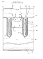
Fig. 1 is an enlarged cross-sectional view illustrating a main portion of a cross-sectional structure taken along the line A1-A2 ofFig. 2 ; -
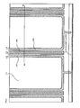
Fig. 2 is a plan view illustrating the planar layout of a main portion of a trench gate IGBT according to Embodiment 1 of the invention; -
Fig. 3 is a cross-sectional view illustrating a main portion of a cross-sectional structure taken along the line B1-B2 ofFig. 4 ; -
Fig. 4 is a plan view illustrating a main portion of a polysilicon gate electrode of a trench gate IGBT including a p-type floating region according to the related art; -
Fig. 5 is a cross-sectional view illustrating a main portion of the trench gate IGBT according to the related art; -
Fig. 6 is a cross-sectional view illustrating a main process of a method for manufacturing the trench gate IGBT according to Embodiment 1 of the invention (part 1); -
Fig. 7 is a cross-sectional view illustrating the main process of the method for manufacturing the trench gate IGBT according to Embodiment 1 of the invention (part 2); -
Fig. 8 is a cross-sectional view illustrating the main process of the method for manufacturing the trench gate IGBT according to Embodiment 1 of the invention (part 3); -
Fig. 9 is a cross-sectional view illustrating the main process of the method for manufacturing the trench gate IGBT according to Embodiment 1 of the invention (part 4); -
Fig. 10 is a cross-sectional view illustrating the main process of the method for manufacturing the trench gate IGBT according to Embodiment 1 of the invention (part 5); and -
Fig. 11 is a cross-sectional view illustrating the main process of the method for manufacturing the trench gate IGBT according to Embodiment 1 of the invention (part 6). - Hereinafter, embodiments of a trench gate MOS semiconductor device and a method for manufacturing the same according to the invention will be described in detail with reference to the drawings. In the specification and the accompanying drawings, in the layers or regions having "n" or "p" appended thereto, an electron or a hole means a majority carrier. In addition, symbols "+" and "-" added to n or p mean that impurity concentration is higher and lower than that of the layer without the symbols. In the description of the following embodiments and the accompanying drawings, the same components are denoted by the same reference numerals and the description thereof will not be repeated. In addition, in the accompanying drawings described in the embodiments, for ease of viewing or understanding, a scale and a dimensional ratio are different from the actual scale and dimensional ratio. The invention is not limited to the following embodiments as long as it does not depart from the scope and spirit thereof. In the specification, in the notation of the Miller indices, "-" means a bar added immediately before an index and "-" added before the index indicates a negative index.
- The structure of a trench gate IGBT according to the invention will be described with reference to
Figs. 1 and2 . -
Fig. 2 is a plan view illustrating the planar layout of a main portion of a trench gate IGBT according to Embodiment 1 of the invention.Fig. 2 illustrates a dividedpolysilicon electrode 21 and a contact portion of the trench gate IGBT according to Embodiment 1 of the invention.Fig. 2 is a plan view illustrating a portion including anactive region 10 that is interposed betweentrenches 15, which are parallel portions of a hatched plane pattern with a stripe shape, a p-type floating region 16 that is surrounded by the ring-shapedtrench 15, and agate runner layer 30 that is provided in the outer circumference of these regions, as viewed from the top.Fig. 1 is an enlarged cross-sectional view illustrating a main portion of the cross-sectional structure taken along the line A1-A2 ofFig. 2 . The trench gate IGBT according to Embodiment 1 of the invention includes a trench gate structure having the dividedpolysilicon electrodes trench 15 and the p-type floating region 16 that does not come into electrical contact with theemitter electrode 24. - Specifically, as illustrated in
Fig. 1 , a p-type base region 17 (and a p+ contact region 18) and an n+ emitter region 19 that is provided in a surface layer along thetrench 15 are provided in the silicon substrate in theactive region 10. Anemitter electrode 24 comes into contact with the surfaces of the two regions through an emittercontact opening portion 27 which is formed in aninterlayer insulating film 25. - In the ring-shaped
trench 15, thepolysilicon gate electrode 21 which is hatched in the drawings, is connected to a gate electrode, and is arranged close to theactive region 10 and thepolysilicon emitter electrode 22 which is connected to theemitter electrode 24 and is arranged close to the p-type floating region 16 are separated and divided. Each of thepolysilicon gate electrodes trench 15, with agate insulating film 20 interposed therebetween. AnHTO film 23 is formed between thepolysilicon gate electrode 21 and thepolysilicon emitter electrode 22 which are separated and divided in thetrench 15. TheHTO film 23 has acavity 26 provided therein and thecavity 26 is closed in the vicinity of an opening portion of thetrench 15. The trench gate IGBT according to the invention is characterized in that thecavity 26 is provided in theHTO film 23 formed in thetrench 15. TheHTO film 23 may be an oxide film formed by a low-temperature chemical vapor deposition (CVD) method. Preferably, the length of thecavity 26 is less than the length of the twopolysilicon electrodes trench 15 in a direction perpendicular to the substrate and the width of thecavity 26 is equal to or more than a quarter of the distance between the boundaries between thegate insulating film 20 and each of thepolysilicon gate electrode 21 and thepolysilicon emitter electrode 22. In this case, it is possible to obtain the effect of suppressing the occurrence of cracks while ensuring the breakdown voltage of the twopolysilicon electrodes trench 15. - In the invention, as described above, the
cavity 26 is provided in theHTO film 23 between thepolysilicon gate electrode 21 and thepolysilicon emitter electrode 22 provided in thetrench 15. Therefore, it is possible to reduce gate capacitance, to suppress the deterioration of switching characteristics, and to reduce switching loss. In addition, even when thepolysilicon gate electrode 21 and thepolysilicon emitter electrode 22 which are connected to different electrodes and have the same potential are separated and divided in thetrench 15, theHTO film 23 provided between the two polysilicon electrodes makes it possible to reliably ensure insulation. In addition, since thecavity 26 provided in theHTO film 23 absorbs stress, it is possible to obtain the effect of reducing or relaxing stress which occurs due to the difference between the thermal expansion coefficients of the oxide film and the polysilicon or silicon substrate. - In addition, the trench gate IGBT according to the invention includes the p-
type floating region 16 which has a higher concentration than the p-type base region 17 and is deeper than thetrench 15. Therefore, it is possible to reduce the on-voltage and to suppress the concentration of the electric field on the bottom of thetrench 15. As a result, it is possible to obtain electrical characteristics without a reduction in breakdown voltage. - As illustrated in
Fig. 2 , thepolysilicon gate electrode 21 which is arranged close to theactive region 10 in thetrench 15 may be connected to thegate runner layer 30 and thepolysilicon emitter electrode 22 which is arranged close to the p-type floating region 16 in thetrench 15 may be connected to an emitterelectrode contact region 31 that is provided in a surface layer of the p-type floating region 16. In this case, for example, it is preferable to formlead trenches trench 15 to thegate runner layer 30 and the p-type floating region 16 in order to facilitate connection to thegate runner layer 30 and the emitterelectrode contact region 31. - In addition, for example, a polyimide film, a nitride film, or an amorphous silicon layer is formed as a passivation film on the
emitter electrode 24, which is not illustrated in the drawings. - As described above, according to Embodiment 1, it is possible to provide a trench gate MOS semiconductor device which has very low gate mirror capacitance and improved turn-on characteristics and reduces the on-voltage and switching loss, with only a slight increase in the number of process steps.
- A method for manufacturing the trench gate MOS semiconductor device according to the invention will be described in detail with reference to
Figs. 6 to 11. Figs. 6 to 11 are cross-sectional views illustrating a main portion of a method for manufacturing the trench gate IGBT according to Embodiment 1 of the invention.Figs. 6 to 11 are the cross-sectional views of a surface layer of the substrate for illustrating the process flow of the structure in which the conductive polysilicon electrodes which are formed in the trench and are the characteristic portions of the trench gate IGBT according to the invention are separated and divided. - In the method for manufacturing the trench gate IGBT according to the invention, first, when the breakdown voltage is in the range of 600 V to 1200 V, an FZ-n semiconductor substrate (silicon substrate) 14 which has a resistivity of about 30 Ωcm to 60 Ωcm and will be a drift layer is prepared. Then, boron (B) ions are implanted with a dose of 5×1014 cm-2 to 3×1015 cm-2, using an insulating film formed on the (100) plane of the FZ-
n semiconductor substrate 14, in order to selectively form the p-type floating region 16. Then, for example, the boron ions in the boron-ion-implanted layer are diffused by a high-temperature diffusion drive of about 1150°C to obtain a p-type region with a depth of about 6 µm to 7 µm. Then, the entire surface of thesubstrate 14 is covered with the insulating film again. Then, thevertical trench 15 which has a stripe-shaped plane pattern and has a width of 1 µm to 3 µm and a depth of about 5 µm is formed from the surface of the substrate by, for example, anisotropic RIE etching so as to be laid across the outer edge of the p-type floating region 16 formed by ion implantation. - Then, the
gate insulating film 20 is formed on the inner wall of thetrench 15, which is vertically formed from the surface of thesilicon substrate 14, by a thermal oxidation method (Fig. 6 ). Then, in thetrench 15, a polysilicon layer is grown to a thickness that does not fill up thetrench 15. For example, it is preferable to grow the polysilicon layer with a thickness of about 0.5 µm with respect to the trench with a width of 2 µm. For example, the polysilicon layer is doped with impurities, such as boron, so as to have conductivity (Fig. 7 ). The conductive polysilicon layer is etched back by an anisotropic etching method such that portions of the conductive polysilicon layer which are disposed on the surface of thesubstrate 14 and at the top and bottom of thetrench 15 are removed as illustrated inFig. 8 . In this way, thepolysilicon gate electrode 21 and thepolysilicon emitter electrode 22 can be formed along the side wall of thetrench 15, with thegate insulating film 20 interposed therebetween. - Then, for example, the
oxide film 23, such as an HTO film or a TEOS film, is formed on the inner surface of thetrench 15 by a CVD method (Fig. 9 ). When theoxide film 23 and thegate insulating film 20 on the surface of the substrate are removed by etching-back, theoxide film 23 having thecavity 26 provided therein is filled between the dividedpolysilicon gate electrode 21 and the divided polysilicon emitter electrode 22 (Fig. 10 ). A process of forming theoxide film 23 will be described in detail below. - Then, the p-
type base region 17 and the n+ emitter region 19 are formed in a portion of the silicon substrate betweenadjacent trenches 15 by a general ion implantation method. Specifically, for example, the p-type base region 17 formed at a depth of 2 µm to 4 µm by the implantation of boron ions with a dose of 1×1013 cm-2 to 1×1014 cm-2 and by thermal diffusion at a temperature of 1150°C. For example, the depth of the p-type base region 17 is less than that of thetrench 15. Then, the n+ emitter region 19 which comes into contact with the side wall of thetrench 15 is selectively formed by ion implantation, using a photoresist formed on the surface of the p-type base region 17 as a mask. It is preferable that the n+ emitter region 19 be formed by the implantation of arsenic (As) ions. - Then, the surface of the p-
type floating region 16 is covered with theinterlayer insulating film 25 such that the p-type floating region 16 is insulated from theemitter electrode 24. Then, an opening portion is provided in the surfaces of the p-type base region 17 and the n+ emitter region 19, which will be theactive region 10, and theemitter electrode 24 is formed by sputter deposition. Theinterlayer insulating film 25 may be, for example, a BPSG film or a PSG film. In addition, a passivation film, such as a polyimide film, is formed on theemitter electrode 24. After the process for the front surface of thesemiconductor substrate 14 ends, the rear surface of thesemiconductor substrate 14 is polished to a predetermined thickness by a chemical mechanical polishing (CMP) apparatus. Then, after a predetermined surface treatment is performed, boron ions are implanted to form a p+ collector layer 13 and acollector electrode 12 comes into ohmic contact with the p+ collector layer 13 (Fig. 11 ). Then, the semiconductor substrate is divided into individual IGBT chips by a dicing process. In this way, the trench gate IGBT is completed. - Next, a process of forming the
oxide film 23 will be described in detail. The conductive polysilicon electrode formed in thetrench 15 is separated and divided into thepolysilicon gate electrode 21 and thepolysilicon emitter electrode 22 at the bottom of thetrench 15 by anisotropic etching. Then, when theHTO film 23 is formed between the dividedpolysilicon electrodes HTO film 23 is closed at the opening portion of thetrench 15 such that thecavity 26 remains along the inner surface of each of thepolysilicon electrodes HTO film 23 having thecavity 26 provided therein is formed between the two polysilicon electrodes by a high-temperature CVD method at a temperature of 700°C to 800°C using silane (SiH4) or nitrous oxide (N2O) as supply gas. It is preferable to use a low-pressure CVD method in which the internal gas pressure of a chamber is in the range of 30 Pa to 200 Pa. The above-mentioned formation conditions of theHTO film 23 enable thecavity 26 to be formed in theHTO film 23 between thepolysilicon gate electrode 21 and thepolysilicon emitter electrode 22. When thecavity 26 is formed in theHTO film 23, the reactivity of gas in the surface increases and gas molecules are less likely to sufficiently flow between thepolysilicon gate electrode 21 and thepolysilicon emitter electrode 22 in thetrench 15. As a result, theHTO film 23 is thick in the vicinity of the opening portion of thetrench 15 and the cavity is likely to be closed. - In the above-described embodiment, the
HTO film 23 has been described. However, a low temperature oxide (LTO) film may be used instead of theHTO film 23. In this case, the LTO film is formed, for example, at a temperature of 400°C, using silane and oxygen (O2) as the supply gas. The internal pressure of the chamber may be in the range of 30 Pa to 200 Pa or may be normal pressure. Similarly to the above, when the LTO film is formed under the above-mentioned conditions, the reactivity of gas in the surface increases and gas molecules are less likely to sufficiently flow between thepolysilicon gate electrode 21 and thepolysilicon emitter electrode 22 in thetrench 15. As a result, thecavity 26 is likely to be closed. - Even when the semiconductor device is exposed to a high-temperature heat treatment environment in the subsequent process, the
cavity 26 absorbs the distortion of stress which occurs in thepolysilicon gate electrode 21 close to theactive region 10 and thepolysilicon emitter electrode 22 close to the p-type floating region 16, which prevents the occurrence of cracks in thepolysilicon electrodes silicon substrate 14. Therefore, an increase in leakage current is suppressed and reliability is improved. In addition, since thecavity 26 is provided between thepolysilicon electrodes trench 15, gate capacitance is reduced, as compared to the device according to the related art in which the opening is filled up with the insulating film without a space therebetween. That is, it is possible to provide a trench gate IGBT which has a small leakage current, low gate mirror capacitance, and improved turn-on characteristics, without significantly increasing the number of process steps. - Various modifications and changes of the invention can be made without departing from the scope and spirit of the invention. For example, the dimensions or impurity concentration of each portion may be set to various values according to required specifications. In the above-described embodiments, the first conductivity type is an n type and the second conductivity type is a p type. However, in the invention, the first conductivity type may be a p type and the second conductivity type may be an n type. In this case, the same effect as described above is obtained.
- As described above, the trench gate MOS semiconductor device and the method for manufacturing the same according to the invention are useful for power semiconductor devices which are used in, for example, power conversion apparatuses or power supply apparatuses of various industrial machines.
-
- 12
- COLLECTOR ELECTRODE
- 13
- p+ COLLECTOR LAYER
- 14
- SEMICONDUCTOR SUBSTRATE (DRIFT LAYER)
- 15
- TRENCH
- 16
- P-TYPE FLOATING REGION
- 17
- P-TYPE BASE REGION
- 19
- n+ EMITTER REGION
- 20
- GATE INSULATING FILM
- 21
- POLYSILICON GATE ELECTRODE
- 22
- POLYSILICON EMITTER ELECTRODE
- 24
- EMITTER ELECTRODE
- 25
- INTERLAYER INSULATING FILM
- 30
- GATE RUNNER LAYER
- 32
- LEAD TRENCH
- 33
- LEAD TRENCH
Claims (6)
- A trench gate MOS semiconductor device comprising:a second-conductivity-type floating region that is provided in a surface layer of one main surface of a first-conductivity-type semiconductor substrate which will be a drift layer;a plurality of trenches that reach a predetermined depth from the surface of the first-conductivity-type semiconductor substrate;a second-conductivity-type base region that is formed in a surface layer of a portion of the first-conductivity-type semiconductor substrate which is interposed between the plurality of trenches arranged in a parallel pattern and is separated from the second-conductivity-type floating region by the trench;a first-conductivity-type emitter region that is formed in a surface layer of the second-conductivity-type base region so as to come into contact with the trench;an emitter electrode that comes into contact with the second-conductivity-type base region and the first-conductivity-type emitter region and covers the second-conductivity-type floating region, with an interlayer insulating film interposed therebetween; anda first conductive polysilicon electrode and a second conductive polysilicon electrode that are formed in the trench along both side surfaces of the trench so as to be separated from each other, with a cavity, which is surrounded by an insulating film, interposed therebetween,wherein the first conductive polysilicon electrode and the second conductive polysilicon electrode are connected to different electrodes.
- The trench gate MOS semiconductor device according to claim 1,
wherein the interlayer insulating film is a BPSG film or a PSG film, and
the insulating film is an HTO film or a TEOS oxide film. - The trench gate MOS semiconductor device according to claim 1,
wherein the first conductive polysilicon electrode is connected to a gate electrode and the second conductive polysilicon electrode is connected to the emitter electrode. - The trench gate MOS semiconductor device according to claim 1, further comprising:a collector electrode that is provided over the other main surface of the first-conductivity-type semiconductor substrate, with a p-type collector layer, which is provided in a surface layer of the other main surface, interposed therebetween.
- The trench gate MOS semiconductor device according to claim 1,
wherein the trench gate MOS semiconductor device is an IGBT. - A method for manufacturing a trench gate MOS semiconductor device including a second-conductivity-type floating region that is provided in a surface layer of one main surface of a first-conductivity-type semiconductor substrate which will be a drift layer, a plurality of trenches that reach a predetermined depth from the surface of the first-conductivity-type semiconductor substrate, a second-conductivity-type base region that is formed in a surface layer of a portion of the first-conductivity-type semiconductor substrate which is interposed between the plurality of trenches arranged in a parallel pattern and is separated from the second-conductivity-type floating region by the trench, a first-conductivity-type emitter region that is formed in a surface layer of the second-conductivity-type base region so as to come into contact with the trench, and an emitter electrode that comes into contact with the second-conductivity-type base region and the first-conductivity-type emitter region and covers the second-conductivity-type floating region, with an interlayer insulating film interposed therebetween, the method comprising:a step of forming the trench at a predetermined depth from the surface of the first-conductivity-type semiconductor substrate;a step of forming, in the trench, a first conductive polysilicon electrode provided along one side wall of the trench and a second conductive polysilicon electrode provided along the other side wall of the trench; anda step of forming an insulating film between the first conductive polysilicon electrode and the second conductive polysilicon electrode using a high-temperature CVD method or a low-temperature CVD method with a reactive gas including a silane gas so as to have a cavity therein.
Applications Claiming Priority (2)
| Application Number | Priority Date | Filing Date | Title |
|---|---|---|---|
| JP2013162948 | 2013-08-06 | ||
| PCT/JP2014/069630 WO2015019862A1 (en) | 2013-08-06 | 2014-07-24 | Trench gate mos semiconductor device and method for manufacturing same |
Publications (3)
| Publication Number | Publication Date |
|---|---|
| EP2955758A1 true EP2955758A1 (en) | 2015-12-16 |
| EP2955758A4 EP2955758A4 (en) | 2016-10-19 |
| EP2955758B1 EP2955758B1 (en) | 2018-03-07 |
Family
ID=52461201
Family Applications (1)
| Application Number | Title | Priority Date | Filing Date |
|---|---|---|---|
| EP14833749.6A Not-in-force EP2955758B1 (en) | 2013-08-06 | 2014-07-24 | Trench gate mos semiconductor device and method for manufacturing same |
Country Status (5)
| Country | Link |
|---|---|
| US (1) | US9461154B2 (en) |
| EP (1) | EP2955758B1 (en) |
| JP (1) | JP5935948B2 (en) |
| CN (1) | CN105027295B (en) |
| WO (1) | WO2015019862A1 (en) |
Cited By (2)
| Publication number | Priority date | Publication date | Assignee | Title |
|---|---|---|---|---|
| EP3460851A1 (en) * | 2017-09-26 | 2019-03-27 | NXP USA, Inc. | Field-effect transistor and method therefor |
| EP3621116A1 (en) * | 2018-09-06 | 2020-03-11 | Infineon Technologies Austria AG | Semiconductor device and manufacturing method thereof |
Families Citing this family (37)
| Publication number | Priority date | Publication date | Assignee | Title |
|---|---|---|---|---|
| JP6420175B2 (en) * | 2014-05-22 | 2018-11-07 | ルネサスエレクトロニクス株式会社 | Semiconductor device |
| US10020362B2 (en) * | 2015-09-04 | 2018-07-10 | Kabushiki Kaisha Toshiba | Semiconductor device and method of manufacturing the same |
| CN107425056A (en) * | 2016-05-24 | 2017-12-01 | 常州中明半导体技术有限公司 | A kind of insulated-gate bipolar transistor device |
| CN108346692B (en) * | 2017-01-25 | 2023-11-21 | 杭州士兰集成电路有限公司 | Power semiconductor device and manufacturing method thereof |
| KR20180104236A (en) * | 2017-03-10 | 2018-09-20 | 매그나칩 반도체 유한회사 | Method of Manufacturing Power Semiconductor Device |
| JP6958093B2 (en) * | 2017-08-09 | 2021-11-02 | 富士電機株式会社 | Semiconductor device |
| US10522677B2 (en) | 2017-09-26 | 2019-12-31 | Nxp Usa, Inc. | Field-effect transistor and method therefor |
| US10600911B2 (en) | 2017-09-26 | 2020-03-24 | Nxp Usa, Inc. | Field-effect transistor and method therefor |
| JP7009933B2 (en) * | 2017-11-03 | 2022-01-26 | 株式会社デンソー | Semiconductor device |
| US10600879B2 (en) | 2018-03-12 | 2020-03-24 | Nxp Usa, Inc. | Transistor trench structure with field plate structures |
| US10833174B2 (en) | 2018-10-26 | 2020-11-10 | Nxp Usa, Inc. | Transistor devices with extended drain regions located in trench sidewalls |
| US10749023B2 (en) | 2018-10-30 | 2020-08-18 | Nxp Usa, Inc. | Vertical transistor with extended drain region |
| US10749028B2 (en) | 2018-11-30 | 2020-08-18 | Nxp Usa, Inc. | Transistor with gate/field plate structure |
| JP7077251B2 (en) * | 2019-02-25 | 2022-05-30 | 株式会社東芝 | Semiconductor device |
| CN110504314B (en) * | 2019-08-30 | 2023-03-03 | 电子科技大学 | Groove-type insulated gate bipolar transistor and preparation method thereof |
| US11387348B2 (en) | 2019-11-22 | 2022-07-12 | Nxp Usa, Inc. | Transistor formed with spacer |
| US11329156B2 (en) | 2019-12-16 | 2022-05-10 | Nxp Usa, Inc. | Transistor with extended drain region |
| JP7249269B2 (en) | 2019-12-27 | 2023-03-30 | 株式会社東芝 | Semiconductor device and its manufacturing method |
| US10937899B1 (en) * | 2020-02-07 | 2021-03-02 | Renesas Electronics Corporation | Semiconductor device |
| CN113497121B (en) * | 2020-03-18 | 2024-04-16 | 芯恩(青岛)集成电路有限公司 | Method for forming split gate trench structure power device |
| US11075110B1 (en) | 2020-03-31 | 2021-07-27 | Nxp Usa, Inc. | Transistor trench with field plate structure |
| US11217675B2 (en) | 2020-03-31 | 2022-01-04 | Nxp Usa, Inc. | Trench with different transverse cross-sectional widths |
| DE102020119738B4 (en) * | 2020-07-27 | 2022-02-03 | Infineon Technologies Dresden GmbH & Co. KG | Process for manufacturing a semiconductor device and semiconductor device with deep trenches |
| JP7438080B2 (en) * | 2020-10-30 | 2024-02-26 | 三菱電機株式会社 | semiconductor equipment |
| JP7446212B2 (en) * | 2020-12-07 | 2024-03-08 | 三菱電機株式会社 | Semiconductor device and its manufacturing method |
| CN114975577B (en) * | 2021-02-19 | 2025-07-29 | 苏州东微半导体股份有限公司 | Semiconductor device with a semiconductor layer having a plurality of semiconductor layers |
| JP7474214B2 (en) | 2021-03-17 | 2024-04-24 | 株式会社東芝 | Semiconductor Device |
| JP7471250B2 (en) * | 2021-03-19 | 2024-04-19 | 株式会社東芝 | Semiconductor Device |
| CN112802841B (en) * | 2021-04-08 | 2021-07-09 | 成都蓉矽半导体有限公司 | A Power MOSFET with Miller Clamping Function |
| DE112022000136T5 (en) * | 2021-05-24 | 2023-06-15 | Fuji Electric Co., Ltd. | SEMICONDUCTOR DEVICE |
| CN116153989A (en) * | 2021-11-23 | 2023-05-23 | 无锡华润华晶微电子有限公司 | IEGT structure and its fabrication method |
| CN114093934B (en) * | 2022-01-20 | 2022-05-20 | 深圳市威兆半导体有限公司 | An IGBT device and its manufacturing method |
| KR20230151276A (en) * | 2022-04-25 | 2023-11-01 | 현대모비스 주식회사 | Power semiconductor device, power semiconductor chip including the same, and method for manufacturing the same |
| TWI810076B (en) * | 2022-09-26 | 2023-07-21 | 國立陽明交通大學 | Gate fabrication method of an u-metal-oxide-semiconductor field-effect transistor and trench gate structure formed thereof |
| CN115775823B (en) * | 2022-11-29 | 2023-07-21 | 上海功成半导体科技有限公司 | Shielding grid power device and preparation method thereof |
| JPWO2025126658A1 (en) * | 2023-12-15 | 2025-06-19 | ||
| CN120825996B (en) * | 2025-09-15 | 2025-12-23 | 杭州谱析光晶半导体科技有限公司 | SiC VDMOSFET structure integrated with gradient strain bar array and preparation process thereof |
Family Cites Families (14)
| Publication number | Priority date | Publication date | Assignee | Title |
|---|---|---|---|---|
| DE69233105T2 (en) | 1991-08-08 | 2004-05-06 | Kabushiki Kaisha Toshiba, Kawasaki | Insulated trench gate bipolar transistor |
| JP4581179B2 (en) | 2000-04-26 | 2010-11-17 | 富士電機システムズ株式会社 | Insulated gate semiconductor device |
| DE10203164B4 (en) * | 2002-01-28 | 2005-06-16 | Infineon Technologies Ag | Power semiconductor component and method for its production |
| JP3930486B2 (en) * | 2004-02-26 | 2007-06-13 | 株式会社東芝 | Semiconductor device and manufacturing method thereof |
| JP2007035841A (en) * | 2005-07-26 | 2007-02-08 | Toshiba Corp | Semiconductor device |
| JP2007180310A (en) | 2005-12-28 | 2007-07-12 | Toshiba Corp | Semiconductor device |
| US7838389B2 (en) * | 2008-05-30 | 2010-11-23 | Freescale Semiconductor, Inc. | Enclosed void cavity for low dielectric constant insulator |
| US7919388B2 (en) * | 2008-05-30 | 2011-04-05 | Freescale Semiconductor, Inc. | Methods for fabricating semiconductor devices having reduced gate-drain capacitance |
| JP2010171074A (en) * | 2009-01-20 | 2010-08-05 | Renesas Technology Corp | Semiconductor device |
| US8319278B1 (en) * | 2009-03-31 | 2012-11-27 | Maxpower Semiconductor, Inc. | Power device structures and methods using empty space zones |
| EP2546882B1 (en) * | 2010-03-09 | 2018-04-18 | Fuji Electric Co., Ltd. | Semiconductor device |
| WO2013001677A1 (en) | 2011-06-28 | 2013-01-03 | パナソニック株式会社 | Semiconductor device and method for manufacturing same |
| JP5059989B1 (en) * | 2011-06-28 | 2012-10-31 | パナソニック株式会社 | Semiconductor device and manufacturing method thereof |
| US8907408B2 (en) * | 2012-03-26 | 2014-12-09 | Infineon Technologies Austria Ag | Stress-reduced field-effect semiconductor device and method for forming therefor |
-
2014
- 2014-07-24 JP JP2015530817A patent/JP5935948B2/en not_active Expired - Fee Related
- 2014-07-24 EP EP14833749.6A patent/EP2955758B1/en not_active Not-in-force
- 2014-07-24 WO PCT/JP2014/069630 patent/WO2015019862A1/en not_active Ceased
- 2014-07-24 CN CN201480013055.4A patent/CN105027295B/en not_active Expired - Fee Related
-
2015
- 2015-09-08 US US14/848,201 patent/US9461154B2/en not_active Expired - Fee Related
Cited By (4)
| Publication number | Priority date | Publication date | Assignee | Title |
|---|---|---|---|---|
| EP3460851A1 (en) * | 2017-09-26 | 2019-03-27 | NXP USA, Inc. | Field-effect transistor and method therefor |
| EP3621116A1 (en) * | 2018-09-06 | 2020-03-11 | Infineon Technologies Austria AG | Semiconductor device and manufacturing method thereof |
| US11316020B2 (en) | 2018-09-06 | 2022-04-26 | Infineon Technologies Austria Ag | Semiconductor device and method |
| US11682704B2 (en) | 2018-09-06 | 2023-06-20 | Infineon Technologies Austria Ag | Method of producing a semiconductor device |
Also Published As
| Publication number | Publication date |
|---|---|
| US9461154B2 (en) | 2016-10-04 |
| JPWO2015019862A1 (en) | 2017-03-02 |
| WO2015019862A1 (en) | 2015-02-12 |
| EP2955758A4 (en) | 2016-10-19 |
| US20150380538A1 (en) | 2015-12-31 |
| CN105027295B (en) | 2018-02-06 |
| EP2955758B1 (en) | 2018-03-07 |
| CN105027295A (en) | 2015-11-04 |
| JP5935948B2 (en) | 2016-06-15 |
Similar Documents
| Publication | Publication Date | Title |
|---|---|---|
| EP2955758B1 (en) | Trench gate mos semiconductor device and method for manufacturing same | |
| TWI518803B (en) | Device structure for high-density MOSFET for load switch and DC-DC device and preparation method thereof | |
| JP5089284B2 (en) | Semiconductor device having a space-saving edge structure | |
| US10020391B2 (en) | Semiconductor device and manufacturing method of the same | |
| TWI512844B (en) | High-frequency switching MOSFET with low output capacitance depleted by P-shield | |
| US9748229B2 (en) | Semiconductor device | |
| EP2822039B1 (en) | Semiconductor device | |
| KR100661109B1 (en) | Vertical semiconductor device and manufacturing method thereof | |
| EP2787534B1 (en) | Insulated gate semiconductor device and method for manufacturing same | |
| TWI412071B (en) | Self-aligned charge-balanced power double-diffused metal oxide semiconductor preparation method | |
| TW201427022A (en) | High-density trench-based power MOSFET with self-aligned active contact and preparation method thereof | |
| US9000516B2 (en) | Super-junction device and method of forming the same | |
| JP6980692B2 (en) | Insulated gate power semiconductor device and its manufacturing method | |
| CN102097470A (en) | Semiconductor device and method for manufacturing the same | |
| CN103890954B (en) | Semiconductor device and method of manufacturing semiconductor device | |
| CN110419111B (en) | Self-aligned and Robust Insulated Gate Bipolar Transistor Devices | |
| CN115939141A (en) | Fully isolated lateral double diffused semiconductor device and method of manufacture | |
| CN113224146B (en) | Transistor devices and methods for fabricating gates of transistor devices | |
| TWI555095B (en) | Semiconductor device and manufacturing method thereof | |
| US7268392B2 (en) | Trench gate semiconductor device with a reduction in switching loss | |
| JP2012195394A (en) | Method of manufacturing semiconductor device | |
| CN112635331A (en) | Preparation method of super junction power device | |
| CN222146233U (en) | Asymmetric SiC withstand voltage MOSFET device | |
| CN116799034A (en) | Semiconductor device and method for manufacturing semiconductor device |
Legal Events
| Date | Code | Title | Description |
|---|---|---|---|
| PUAI | Public reference made under article 153(3) epc to a published international application that has entered the european phase |
Free format text: ORIGINAL CODE: 0009012 |
|
| 17P | Request for examination filed |
Effective date: 20150909 |
|
| AK | Designated contracting states |
Kind code of ref document: A1 Designated state(s): AL AT BE BG CH CY CZ DE DK EE ES FI FR GB GR HR HU IE IS IT LI LT LU LV MC MK MT NL NO PL PT RO RS SE SI SK SM TR |
|
| AX | Request for extension of the european patent |
Extension state: BA ME |
|
| A4 | Supplementary search report drawn up and despatched |
Effective date: 20160920 |
|
| RIC1 | Information provided on ipc code assigned before grant |
Ipc: H01L 29/78 20060101AFI20160914BHEP Ipc: H01L 29/739 20060101ALI20160914BHEP Ipc: H01L 29/423 20060101ALI20160914BHEP Ipc: H01L 29/40 20060101ALI20160914BHEP Ipc: H01L 21/02 20060101ALN20160914BHEP Ipc: H01L 21/28 20060101ALI20160914BHEP Ipc: H01L 29/66 20060101ALI20160914BHEP Ipc: H01L 29/10 20060101ALN20160914BHEP Ipc: H01L 29/49 20060101ALI20160914BHEP Ipc: H01L 29/06 20060101ALI20160914BHEP Ipc: H01L 21/316 20060101ALI20160914BHEP |
|
| DAX | Request for extension of the european patent (deleted) | ||
| GRAP | Despatch of communication of intention to grant a patent |
Free format text: ORIGINAL CODE: EPIDOSNIGR1 |
|
| STAA | Information on the status of an ep patent application or granted ep patent |
Free format text: STATUS: GRANT OF PATENT IS INTENDED |
|
| RIC1 | Information provided on ipc code assigned before grant |
Ipc: H01L 29/739 20060101ALI20170426BHEP Ipc: H01L 29/40 20060101ALI20170426BHEP Ipc: H01L 29/06 20060101ALI20170426BHEP Ipc: H01L 29/10 20060101ALN20170426BHEP Ipc: H01L 21/02 20060101ALN20170426BHEP Ipc: H01L 21/331 20060101ALI20170426BHEP Ipc: H01L 29/423 20060101AFI20170426BHEP |
|
| RIC1 | Information provided on ipc code assigned before grant |
Ipc: H01L 29/739 20060101ALI20170428BHEP Ipc: H01L 21/02 20060101ALN20170428BHEP Ipc: H01L 21/331 20060101ALI20170428BHEP Ipc: H01L 29/06 20060101ALI20170428BHEP Ipc: H01L 29/423 20060101AFI20170428BHEP Ipc: H01L 29/40 20060101ALI20170428BHEP Ipc: H01L 29/10 20060101ALN20170428BHEP |
|
| INTG | Intention to grant announced |
Effective date: 20170519 |
|
| GRAJ | Information related to disapproval of communication of intention to grant by the applicant or resumption of examination proceedings by the epo deleted |
Free format text: ORIGINAL CODE: EPIDOSDIGR1 |
|
| STAA | Information on the status of an ep patent application or granted ep patent |
Free format text: STATUS: REQUEST FOR EXAMINATION WAS MADE |
|
| REG | Reference to a national code |
Ref country code: DE Ref legal event code: R079 Ref document number: 602014022186 Country of ref document: DE Free format text: PREVIOUS MAIN CLASS: H01L0029780000 Ipc: H01L0029423000 |
|
| GRAP | Despatch of communication of intention to grant a patent |
Free format text: ORIGINAL CODE: EPIDOSNIGR1 |
|
| STAA | Information on the status of an ep patent application or granted ep patent |
Free format text: STATUS: GRANT OF PATENT IS INTENDED |
|
| RAP1 | Party data changed (applicant data changed or rights of an application transferred) |
Owner name: FUJI ELECTRIC CO., LTD. |
|
| RIN1 | Information on inventor provided before grant (corrected) |
Inventor name: OGAWA, ERI |
|
| INTC | Intention to grant announced (deleted) | ||
| RIC1 | Information provided on ipc code assigned before grant |
Ipc: H01L 29/40 20060101ALI20170913BHEP Ipc: H01L 29/06 20060101ALI20170913BHEP Ipc: H01L 21/02 20060101ALN20170913BHEP Ipc: H01L 29/10 20060101ALN20170913BHEP Ipc: H01L 29/423 20060101AFI20170913BHEP Ipc: H01L 21/331 20060101ALI20170913BHEP Ipc: H01L 29/739 20060101ALI20170913BHEP |
|
| INTG | Intention to grant announced |
Effective date: 20170926 |
|
| GRAS | Grant fee paid |
Free format text: ORIGINAL CODE: EPIDOSNIGR3 |
|
| GRAA | (expected) grant |
Free format text: ORIGINAL CODE: 0009210 |
|
| STAA | Information on the status of an ep patent application or granted ep patent |
Free format text: STATUS: THE PATENT HAS BEEN GRANTED |
|
| AK | Designated contracting states |
Kind code of ref document: B1 Designated state(s): AL AT BE BG CH CY CZ DE DK EE ES FI FR GB GR HR HU IE IS IT LI LT LU LV MC MK MT NL NO PL PT RO RS SE SI SK SM TR |
|
| REG | Reference to a national code |
Ref country code: GB Ref legal event code: FG4D |
|
| REG | Reference to a national code |
Ref country code: CH Ref legal event code: EP Ref country code: AT Ref legal event code: REF Ref document number: 977412 Country of ref document: AT Kind code of ref document: T Effective date: 20180315 |
|
| REG | Reference to a national code |
Ref country code: DE Ref legal event code: R096 Ref document number: 602014022186 Country of ref document: DE |
|
| REG | Reference to a national code |
Ref country code: IE Ref legal event code: FG4D |
|
| REG | Reference to a national code |
Ref country code: NL Ref legal event code: MP Effective date: 20180307 |
|
| REG | Reference to a national code |
Ref country code: LT Ref legal event code: MG4D |
|
| PG25 | Lapsed in a contracting state [announced via postgrant information from national office to epo] |
Ref country code: FI Free format text: LAPSE BECAUSE OF FAILURE TO SUBMIT A TRANSLATION OF THE DESCRIPTION OR TO PAY THE FEE WITHIN THE PRESCRIBED TIME-LIMIT Effective date: 20180307 Ref country code: NO Free format text: LAPSE BECAUSE OF FAILURE TO SUBMIT A TRANSLATION OF THE DESCRIPTION OR TO PAY THE FEE WITHIN THE PRESCRIBED TIME-LIMIT Effective date: 20180607 Ref country code: CY Free format text: LAPSE BECAUSE OF FAILURE TO SUBMIT A TRANSLATION OF THE DESCRIPTION OR TO PAY THE FEE WITHIN THE PRESCRIBED TIME-LIMIT Effective date: 20180307 Ref country code: ES Free format text: LAPSE BECAUSE OF FAILURE TO SUBMIT A TRANSLATION OF THE DESCRIPTION OR TO PAY THE FEE WITHIN THE PRESCRIBED TIME-LIMIT Effective date: 20180307 Ref country code: LT Free format text: LAPSE BECAUSE OF FAILURE TO SUBMIT A TRANSLATION OF THE DESCRIPTION OR TO PAY THE FEE WITHIN THE PRESCRIBED TIME-LIMIT Effective date: 20180307 Ref country code: HR Free format text: LAPSE BECAUSE OF FAILURE TO SUBMIT A TRANSLATION OF THE DESCRIPTION OR TO PAY THE FEE WITHIN THE PRESCRIBED TIME-LIMIT Effective date: 20180307 |
|
| REG | Reference to a national code |
Ref country code: AT Ref legal event code: MK05 Ref document number: 977412 Country of ref document: AT Kind code of ref document: T Effective date: 20180307 |
|
| PG25 | Lapsed in a contracting state [announced via postgrant information from national office to epo] |
Ref country code: GR Free format text: LAPSE BECAUSE OF FAILURE TO SUBMIT A TRANSLATION OF THE DESCRIPTION OR TO PAY THE FEE WITHIN THE PRESCRIBED TIME-LIMIT Effective date: 20180608 Ref country code: BG Free format text: LAPSE BECAUSE OF FAILURE TO SUBMIT A TRANSLATION OF THE DESCRIPTION OR TO PAY THE FEE WITHIN THE PRESCRIBED TIME-LIMIT Effective date: 20180607 Ref country code: RS Free format text: LAPSE BECAUSE OF FAILURE TO SUBMIT A TRANSLATION OF THE DESCRIPTION OR TO PAY THE FEE WITHIN THE PRESCRIBED TIME-LIMIT Effective date: 20180307 Ref country code: SE Free format text: LAPSE BECAUSE OF FAILURE TO SUBMIT A TRANSLATION OF THE DESCRIPTION OR TO PAY THE FEE WITHIN THE PRESCRIBED TIME-LIMIT Effective date: 20180307 Ref country code: LV Free format text: LAPSE BECAUSE OF FAILURE TO SUBMIT A TRANSLATION OF THE DESCRIPTION OR TO PAY THE FEE WITHIN THE PRESCRIBED TIME-LIMIT Effective date: 20180307 |
|
| PG25 | Lapsed in a contracting state [announced via postgrant information from national office to epo] |
Ref country code: PL Free format text: LAPSE BECAUSE OF FAILURE TO SUBMIT A TRANSLATION OF THE DESCRIPTION OR TO PAY THE FEE WITHIN THE PRESCRIBED TIME-LIMIT Effective date: 20180307 Ref country code: EE Free format text: LAPSE BECAUSE OF FAILURE TO SUBMIT A TRANSLATION OF THE DESCRIPTION OR TO PAY THE FEE WITHIN THE PRESCRIBED TIME-LIMIT Effective date: 20180307 Ref country code: RO Free format text: LAPSE BECAUSE OF FAILURE TO SUBMIT A TRANSLATION OF THE DESCRIPTION OR TO PAY THE FEE WITHIN THE PRESCRIBED TIME-LIMIT Effective date: 20180307 Ref country code: NL Free format text: LAPSE BECAUSE OF FAILURE TO SUBMIT A TRANSLATION OF THE DESCRIPTION OR TO PAY THE FEE WITHIN THE PRESCRIBED TIME-LIMIT Effective date: 20180307 Ref country code: IT Free format text: LAPSE BECAUSE OF FAILURE TO SUBMIT A TRANSLATION OF THE DESCRIPTION OR TO PAY THE FEE WITHIN THE PRESCRIBED TIME-LIMIT Effective date: 20180307 Ref country code: AL Free format text: LAPSE BECAUSE OF FAILURE TO SUBMIT A TRANSLATION OF THE DESCRIPTION OR TO PAY THE FEE WITHIN THE PRESCRIBED TIME-LIMIT Effective date: 20180307 |
|
| PG25 | Lapsed in a contracting state [announced via postgrant information from national office to epo] |
Ref country code: SK Free format text: LAPSE BECAUSE OF FAILURE TO SUBMIT A TRANSLATION OF THE DESCRIPTION OR TO PAY THE FEE WITHIN THE PRESCRIBED TIME-LIMIT Effective date: 20180307 Ref country code: AT Free format text: LAPSE BECAUSE OF FAILURE TO SUBMIT A TRANSLATION OF THE DESCRIPTION OR TO PAY THE FEE WITHIN THE PRESCRIBED TIME-LIMIT Effective date: 20180307 Ref country code: SM Free format text: LAPSE BECAUSE OF FAILURE TO SUBMIT A TRANSLATION OF THE DESCRIPTION OR TO PAY THE FEE WITHIN THE PRESCRIBED TIME-LIMIT Effective date: 20180307 Ref country code: CZ Free format text: LAPSE BECAUSE OF FAILURE TO SUBMIT A TRANSLATION OF THE DESCRIPTION OR TO PAY THE FEE WITHIN THE PRESCRIBED TIME-LIMIT Effective date: 20180307 |
|
| REG | Reference to a national code |
Ref country code: DE Ref legal event code: R097 Ref document number: 602014022186 Country of ref document: DE |
|
| PG25 | Lapsed in a contracting state [announced via postgrant information from national office to epo] |
Ref country code: PT Free format text: LAPSE BECAUSE OF FAILURE TO SUBMIT A TRANSLATION OF THE DESCRIPTION OR TO PAY THE FEE WITHIN THE PRESCRIBED TIME-LIMIT Effective date: 20180709 |
|
| PLBE | No opposition filed within time limit |
Free format text: ORIGINAL CODE: 0009261 |
|
| STAA | Information on the status of an ep patent application or granted ep patent |
Free format text: STATUS: NO OPPOSITION FILED WITHIN TIME LIMIT |
|
| PG25 | Lapsed in a contracting state [announced via postgrant information from national office to epo] |
Ref country code: DK Free format text: LAPSE BECAUSE OF FAILURE TO SUBMIT A TRANSLATION OF THE DESCRIPTION OR TO PAY THE FEE WITHIN THE PRESCRIBED TIME-LIMIT Effective date: 20180307 |
|
| 26N | No opposition filed |
Effective date: 20181210 |
|
| PG25 | Lapsed in a contracting state [announced via postgrant information from national office to epo] |
Ref country code: SI Free format text: LAPSE BECAUSE OF FAILURE TO SUBMIT A TRANSLATION OF THE DESCRIPTION OR TO PAY THE FEE WITHIN THE PRESCRIBED TIME-LIMIT Effective date: 20180307 |
|
| REG | Reference to a national code |
Ref country code: CH Ref legal event code: PL |
|
| GBPC | Gb: european patent ceased through non-payment of renewal fee |
Effective date: 20180724 |
|
| PG25 | Lapsed in a contracting state [announced via postgrant information from national office to epo] |
Ref country code: LU Free format text: LAPSE BECAUSE OF NON-PAYMENT OF DUE FEES Effective date: 20180724 Ref country code: MC Free format text: LAPSE BECAUSE OF FAILURE TO SUBMIT A TRANSLATION OF THE DESCRIPTION OR TO PAY THE FEE WITHIN THE PRESCRIBED TIME-LIMIT Effective date: 20180307 |
|
| REG | Reference to a national code |
Ref country code: BE Ref legal event code: MM Effective date: 20180731 |
|
| REG | Reference to a national code |
Ref country code: IE Ref legal event code: MM4A |
|
| PG25 | Lapsed in a contracting state [announced via postgrant information from national office to epo] |
Ref country code: FR Free format text: LAPSE BECAUSE OF NON-PAYMENT OF DUE FEES Effective date: 20180731 Ref country code: GB Free format text: LAPSE BECAUSE OF NON-PAYMENT OF DUE FEES Effective date: 20180724 Ref country code: LI Free format text: LAPSE BECAUSE OF NON-PAYMENT OF DUE FEES Effective date: 20180731 Ref country code: IE Free format text: LAPSE BECAUSE OF NON-PAYMENT OF DUE FEES Effective date: 20180724 Ref country code: CH Free format text: LAPSE BECAUSE OF NON-PAYMENT OF DUE FEES Effective date: 20180731 |
|
| PG25 | Lapsed in a contracting state [announced via postgrant information from national office to epo] |
Ref country code: BE Free format text: LAPSE BECAUSE OF NON-PAYMENT OF DUE FEES Effective date: 20180731 |
|
| PG25 | Lapsed in a contracting state [announced via postgrant information from national office to epo] |
Ref country code: MT Free format text: LAPSE BECAUSE OF NON-PAYMENT OF DUE FEES Effective date: 20180724 |
|
| PG25 | Lapsed in a contracting state [announced via postgrant information from national office to epo] |
Ref country code: TR Free format text: LAPSE BECAUSE OF FAILURE TO SUBMIT A TRANSLATION OF THE DESCRIPTION OR TO PAY THE FEE WITHIN THE PRESCRIBED TIME-LIMIT Effective date: 20180307 |
|
| PG25 | Lapsed in a contracting state [announced via postgrant information from national office to epo] |
Ref country code: HU Free format text: LAPSE BECAUSE OF FAILURE TO SUBMIT A TRANSLATION OF THE DESCRIPTION OR TO PAY THE FEE WITHIN THE PRESCRIBED TIME-LIMIT; INVALID AB INITIO Effective date: 20140724 Ref country code: MK Free format text: LAPSE BECAUSE OF NON-PAYMENT OF DUE FEES Effective date: 20180307 |
|
| PG25 | Lapsed in a contracting state [announced via postgrant information from national office to epo] |
Ref country code: IS Free format text: LAPSE BECAUSE OF FAILURE TO SUBMIT A TRANSLATION OF THE DESCRIPTION OR TO PAY THE FEE WITHIN THE PRESCRIBED TIME-LIMIT Effective date: 20180707 |
|
| PGFP | Annual fee paid to national office [announced via postgrant information from national office to epo] |
Ref country code: DE Payment date: 20220531 Year of fee payment: 9 |
|
| REG | Reference to a national code |
Ref country code: DE Ref legal event code: R119 Ref document number: 602014022186 Country of ref document: DE |
|
| PG25 | Lapsed in a contracting state [announced via postgrant information from national office to epo] |
Ref country code: DE Free format text: LAPSE BECAUSE OF NON-PAYMENT OF DUE FEES Effective date: 20240201 |