EP2954341B1 - Magnetic field sensor comprising angle correction module - Google Patents
Magnetic field sensor comprising angle correction module Download PDFInfo
- Publication number
- EP2954341B1 EP2954341B1 EP14702173.7A EP14702173A EP2954341B1 EP 2954341 B1 EP2954341 B1 EP 2954341B1 EP 14702173 A EP14702173 A EP 14702173A EP 2954341 B1 EP2954341 B1 EP 2954341B1
- Authority
- EP
- European Patent Office
- Prior art keywords
- value
- angle
- magnetic field
- temperature
- error
- Prior art date
- Legal status (The legal status is an assumption and is not a legal conclusion. Google has not performed a legal analysis and makes no representation as to the accuracy of the status listed.)
- Active
Links
- 230000005291 magnetic effect Effects 0.000 title claims description 234
- 238000012937 correction Methods 0.000 title claims description 180
- 230000008859 change Effects 0.000 claims description 51
- 238000000034 method Methods 0.000 claims description 49
- 239000000758 substrate Substances 0.000 claims description 30
- 230000005355 Hall effect Effects 0.000 claims description 17
- 239000004065 semiconductor Substances 0.000 claims description 13
- 230000004044 response Effects 0.000 claims description 11
- 238000009792 diffusion process Methods 0.000 claims description 10
- 239000007943 implant Substances 0.000 claims description 10
- 230000001419 dependent effect Effects 0.000 claims description 8
- 238000001514 detection method Methods 0.000 claims description 6
- 238000012545 processing Methods 0.000 claims description 4
- 238000009987 spinning Methods 0.000 description 103
- ORQBXQOJMQIAOY-UHFFFAOYSA-N nobelium Chemical compound [No] ORQBXQOJMQIAOY-UHFFFAOYSA-N 0.000 description 44
- 238000000819 phase cycle Methods 0.000 description 33
- 230000003595 spectral effect Effects 0.000 description 17
- 230000006870 function Effects 0.000 description 10
- 230000008878 coupling Effects 0.000 description 8
- 238000010168 coupling process Methods 0.000 description 8
- 238000005859 coupling reaction Methods 0.000 description 8
- 230000035945 sensitivity Effects 0.000 description 6
- PCTMTFRHKVHKIS-BMFZQQSSSA-N (1s,3r,4e,6e,8e,10e,12e,14e,16e,18s,19r,20r,21s,25r,27r,30r,31r,33s,35r,37s,38r)-3-[(2r,3s,4s,5s,6r)-4-amino-3,5-dihydroxy-6-methyloxan-2-yl]oxy-19,25,27,30,31,33,35,37-octahydroxy-18,20,21-trimethyl-23-oxo-22,39-dioxabicyclo[33.3.1]nonatriaconta-4,6,8,10 Chemical compound C1C=C2C[C@@H](OS(O)(=O)=O)CC[C@]2(C)[C@@H]2[C@@H]1[C@@H]1CC[C@H]([C@H](C)CCCC(C)C)[C@@]1(C)CC2.O[C@H]1[C@@H](N)[C@H](O)[C@@H](C)O[C@H]1O[C@H]1/C=C/C=C/C=C/C=C/C=C/C=C/C=C/[C@H](C)[C@@H](O)[C@@H](C)[C@H](C)OC(=O)C[C@H](O)C[C@H](O)CC[C@@H](O)[C@H](O)C[C@H](O)C[C@](O)(C[C@H](O)[C@H]2C(O)=O)O[C@H]2C1 PCTMTFRHKVHKIS-BMFZQQSSSA-N 0.000 description 5
- 101100321992 Drosophila melanogaster ABCD gene Proteins 0.000 description 5
- 238000012163 sequencing technique Methods 0.000 description 5
- 238000004364 calculation method Methods 0.000 description 4
- 238000010586 diagram Methods 0.000 description 4
- 238000012546 transfer Methods 0.000 description 4
- 238000004891 communication Methods 0.000 description 3
- VUFOSBDICLTFMS-UHFFFAOYSA-M ethyl-hexadecyl-dimethylazanium;bromide Chemical compound [Br-].CCCCCCCCCCCCCCCC[N+](C)(C)CC VUFOSBDICLTFMS-UHFFFAOYSA-M 0.000 description 3
- 230000005294 ferromagnetic effect Effects 0.000 description 3
- 230000008569 process Effects 0.000 description 3
- 230000003252 repetitive effect Effects 0.000 description 3
- 230000009977 dual effect Effects 0.000 description 2
- WPYVAWXEWQSOGY-UHFFFAOYSA-N indium antimonide Chemical compound [Sb]#[In] WPYVAWXEWQSOGY-UHFFFAOYSA-N 0.000 description 2
- 238000002347 injection Methods 0.000 description 2
- 239000007924 injection Substances 0.000 description 2
- 238000002955 isolation Methods 0.000 description 2
- 239000000463 material Substances 0.000 description 2
- 229910052751 metal Inorganic materials 0.000 description 2
- 239000002184 metal Substances 0.000 description 2
- -1 type III-V Chemical class 0.000 description 2
- WPWLFFMSSOAORQ-UHFFFAOYSA-N 5-bromo-4-chloro-3-indolyl acetate Chemical compound C1=C(Br)C(Cl)=C2C(OC(=O)C)=CNC2=C1 WPWLFFMSSOAORQ-UHFFFAOYSA-N 0.000 description 1
- JBRZTFJDHDCESZ-UHFFFAOYSA-N AsGa Chemical compound [As]#[Ga] JBRZTFJDHDCESZ-UHFFFAOYSA-N 0.000 description 1
- XUIMIQQOPSSXEZ-UHFFFAOYSA-N Silicon Chemical compound [Si] XUIMIQQOPSSXEZ-UHFFFAOYSA-N 0.000 description 1
- 230000001174 ascending effect Effects 0.000 description 1
- 230000006399 behavior Effects 0.000 description 1
- 150000001875 compounds Chemical class 0.000 description 1
- 239000004020 conductor Substances 0.000 description 1
- 238000013461 design Methods 0.000 description 1
- 229910052732 germanium Inorganic materials 0.000 description 1
- GNPVGFCGXDBREM-UHFFFAOYSA-N germanium atom Chemical compound [Ge] GNPVGFCGXDBREM-UHFFFAOYSA-N 0.000 description 1
- 150000002472 indium compounds Chemical class 0.000 description 1
- 238000002372 labelling Methods 0.000 description 1
- 230000005381 magnetic domain Effects 0.000 description 1
- 230000010363 phase shift Effects 0.000 description 1
- 230000009467 reduction Effects 0.000 description 1
- 229910052710 silicon Inorganic materials 0.000 description 1
- 239000010703 silicon Substances 0.000 description 1
- 230000005641 tunneling Effects 0.000 description 1
Images


Classifications
-
- G—PHYSICS
- G01—MEASURING; TESTING
- G01B—MEASURING LENGTH, THICKNESS OR SIMILAR LINEAR DIMENSIONS; MEASURING ANGLES; MEASURING AREAS; MEASURING IRREGULARITIES OF SURFACES OR CONTOURS
- G01B7/00—Measuring arrangements characterised by the use of electric or magnetic techniques
- G01B7/02—Measuring arrangements characterised by the use of electric or magnetic techniques for measuring length, width or thickness
- G01B7/023—Measuring arrangements characterised by the use of electric or magnetic techniques for measuring length, width or thickness for measuring distance between sensor and object
-
- G—PHYSICS
- G01—MEASURING; TESTING
- G01R—MEASURING ELECTRIC VARIABLES; MEASURING MAGNETIC VARIABLES
- G01R33/00—Arrangements or instruments for measuring magnetic variables
- G01R33/0023—Electronic aspects, e.g. circuits for stimulation, evaluation, control; Treating the measured signals; calibration
-
- G—PHYSICS
- G01—MEASURING; TESTING
- G01R—MEASURING ELECTRIC VARIABLES; MEASURING MAGNETIC VARIABLES
- G01R33/00—Arrangements or instruments for measuring magnetic variables
- G01R33/007—Environmental aspects, e.g. temperature variations, radiation, stray fields
-
- G—PHYSICS
- G01—MEASURING; TESTING
- G01R—MEASURING ELECTRIC VARIABLES; MEASURING MAGNETIC VARIABLES
- G01R33/00—Arrangements or instruments for measuring magnetic variables
- G01R33/02—Measuring direction or magnitude of magnetic fields or magnetic flux
- G01R33/06—Measuring direction or magnitude of magnetic fields or magnetic flux using galvano-magnetic devices
- G01R33/07—Hall effect devices
- G01R33/077—Vertical Hall-effect devices
-
- G—PHYSICS
- G01—MEASURING; TESTING
- G01R—MEASURING ELECTRIC VARIABLES; MEASURING MAGNETIC VARIABLES
- G01R33/00—Arrangements or instruments for measuring magnetic variables
- G01R33/02—Measuring direction or magnitude of magnetic fields or magnetic flux
- G01R33/06—Measuring direction or magnitude of magnetic fields or magnetic flux using galvano-magnetic devices
- G01R33/07—Hall effect devices
- G01R33/072—Constructional adaptation of the sensor to specific applications
- G01R33/075—Hall devices configured for spinning current measurements
Definitions
- This invention relates generally to magnetic field sensors and, more particularly, to a magnetic field sensor that can provide an output signal representative of an angle of rotation of a target object, for which angular errors are reduced.
- Magnetic field sensing elements can be used in a variety of applications.
- a magnetic field sensing element can be used to detect a direction of a magnetic field, i.e., and angle of the direction of the magnetic field.
- Planar Hall elements and vertical Hall elements are known types of magnetic field sensing elements.
- a planar Hall element tends to be responsive to magnetic field perpendicular to a surface of a substrate on which the planar Hall element is formed.
- a vertical Hall element tends to be responsive to magnetic field parallel to a surface of a substrate on which the vertical Hall element is formed.
- CVH circular vertical Hall
- PCT Patent Application No. PCT/EP2008/056517 entitled “Magnetic Field Sensor for Measuring Direction of a Magnetic Field in a Plane,” filed May 28, 2008, and published in the English language as PCT Publication No. WO 2008/145662 .
- the CVH sensing element is a circular arrangement of vertical Hall elements arranged over a common circular implant and diffusion region in a substrate.
- the common implant and diffusion region can be a common epi (epitaxial) region (e.g., layer) upon a substrate, bounded by semiconductor isolation structures.
- the CVH sensing element can be used to sense a direction (i.e., an angle) (and optionally a strength) of a magnetic field in a plane of the substrate.
- Various parameters characterize the performance of magnetic field sensing elements and magnetic field sensors that use magnetic field sensing elements. These parameters include sensitivity, which is a change in an output signal of a magnetic field sensing element in response to a change of magnetic field experienced by the magnetic sensing element, and linearity, which is a degree to which the output signal of the magnetic field sensing element varies in direct proportion to the magnetic field. These parameters also include an offset, which is characterized by an output signal from the magnetic field sensing element not representative of a zero magnetic field when the magnetic field sensing element experiences a zero magnetic field.
- the above-described CVH sensing element is operable, with associated circuits, to provide an output signal representative of an angle of a direction of a magnetic field. Therefore, as described below, if a magnet is disposed upon or otherwise coupled to a so-called "target object," for example, a camshaft in an engine, the CVH sensing element can be used to provide an output signal representative of an angle of rotation of the target object.
- target object for example, a camshaft in an engine
- the CVH sensing element is but one element that can provide an output signal representative of an angle of a magnetic field, i.e., an angle sensor.
- an angle sensor can be provided from a plurality of separate vertical Hall elements or a plurality of magnetoresistance elements.
- magnetic field sensing element(s) that generate an output signal related to an angle of a magnetic field are referred to herein "angle sensing elements.”
- More parameters can characterize the performance of and angle sensing element(s), e.g., a CVH sensing element
- One such parameter is an angular accuracy of the output signal generated by the angle sensing elements).
- Angular accuracy can have both an average angle error that is the same at all magnetic field pointing angles, and also an angle error that is different at different magnetic field angles (i.e. a non-linearity error).
- Another parameter is the speed with which the angle sensing element(s) can convey the angle of the magnetic field. It will be understood that the speed is particularly important for applications in which the angle of the magnetic field may be rapidly changing.
- US 2005/278137 A1 discloses a method for adjusting a determination rule for an error compensation of an angle sensor, which is designed to detect a first component of a direction along a first axis and a second component of a direction along a second axis, and to determine an angle of the direction according to the determination rule based on the first and second components.
- the method includes: detecting values of component pairs consisting of two predetermined components for the calculation of offset and/or amplitude and/or axis-angle errors.
- US 2012/095712 A1 discloses an angle detection unit including first to third arithmetic units which receives first and second signals that are associated with intensities of components of a rotating magnetic field in mutually different directions.
- the first arithmetic unit generates a sum of squares signal made up of the sum of squares of the first and second signals.
- the second arithmetic unit calculates a first error component estimate which is an estimated value of a first error component included in the first signal and a second error component estimate which is an estimated value of a second error component included in the second signal.
- the third arithmetic unit generates a first corrected signal by subtracting the first error component estimate from the first signal, generates a second corrected signal by subtracting the second error component estimate from the second signal, and calculates a detected angle value based on the first and second corrected signals.
- WO 98/02721 A2 discloses a digital compensation circuit for calibrating a sensor.
- the compensator circuit comprises a serial communication circuit for receiving data relating to a plurality of parameters, and means coupled to serial communication circuit for providing piece-wise linear compensation of a temperature coefficient.
- the piece-wise linear compensation means further comprises detector means for detecting a threshold for a digital temperature and providing an output, and a plurality of registers coupled to the detector means and the serial communication circuit, a first of the plurality of registers for providing a first value if the digital temperature is above the threshold, a second of the plurality of registers for providing a second value if the digital temperature is below the threshold.
- the piece-wise linear compensation means further includes a selector means coupled to the detector means and the plurality of registers for selecting one of the first and second of the plurality of registers dependent upon the output of the detector means for providing piece-wise linear compensation of a temperature coefficient.
- US 2012/086442 A1 discloses a magnetic field sensor and a method associated with the magnetic field sensor, which provide gain correction coefficients and/or offset correction coefficients stored in the magnetic field sensor in digital form.
- the gain correction coefficients and/or offset correction coefficients can be used to generate analog control signals to control a sensitivity and/or an offset of an analog signal path through the magnetic field sensor.
- the present invention provides circuits and techniques that can process output signals from an angle sensing element to provide an output signal that has a high degree of angle accuracy and a relatively high speed.
- a magnetic field sensor includes a plurality of magnetic field sensing elements, each one of the plurality of magnetic field sensing elements is configured to generate a respective x-y output signal responsive to a magnetic field in an x-y plane.
- the magnetic field sensor also includes an angle processing circuit coupled to receive the x-y output signals and configured to generate an uncorrected x-y angle value representative of an angle of the magnetic field in an x-y plane.
- the uncorrected x-y angle value has a first angle error component.
- the magnetic field sensor also includes an angle error correction module coupled to the angle processing circuit and configured to generate an x-y angle error value indicative of an error in the uncorrected x-y angle value.
- the magnetic field sensor also includes a combining module configured to combine the uncorrected x-y angle value with the x-y angle error value to generate a corrected x-y angle value having a second angle error component smaller than the first angle error component.
- the above magnetic field sensor further Includes a sine lookup table for storing a plurality of sine values, wherein the algorithm module is coupled to receive a sine value selected from among the plurality of sine values and to apply the algorithm also using the selected sine value.
- the above magnetic field sensor can include one or more of the following aspects, in any combination.
- the plurality of magnetic field sensing elements comprises a plurality of vertical Hall Effect elements arranged as a circular vertical Hall (CVH) element, wherein each one of the plurality of vertical Hall Effect elements is arranged upon a common circular implant and diffusion region in a first major surface of a semiconductor substrate, wherein the plurality of vertical Hall Effect elements is configured to generate a respective plurality of x-y output signals responsive to a magnetic field having a direction component in an x-y plane parallel to the first surface of the semiconductor substrate, the x-y plane having an x-direction and a y-direction orthogonal to the x-direction, wherein the plurality of x-y output signals is generated in a plurality of cycle periods, each cycle period corresponding to one cycle around the CVH sensing element, the cycle periods occurring at a cycle rate.
- CVH circular vertical Hall
- the selected sine value is selected in accordance with the uncorrected x-y angle value.
- the selected sine value is selected in accordance with the x-y angle value and in accordance with an interpolated phase coefficient.
- the angle error correction module is configured to use a temperature-dependent sinusoidal error relationship to describe the first angle error component, sinusoidal with respect to the angle of the magnetic field, and wherein the plurality of correction coefficients comprises: a plurality of correction coefficients representative of respective magnitudes and phases of one or more harmonics of the sinusoidal error relationship at a corresponding plurality of different temperatures.
- the plurality of correction coefficients further comprises a plurality of correction coefficients representative of respective magnitudes and phases of first and second harmonics of the sinusoidal error relationship at a corresponding plurality of different temperatures.
- the plurality of correction coefficients further comprises a plurality of correction coefficients representative of respective magnitudes of average angle errors of the sinusoidal error relationship at a corresponding plurality of different temperatures.
- the above magnetic field sensor further includes a program control register coupled to receive a program control value, wherein the interpolation module is coupled to receive a value representative of the program control value, and, in response to the program control value, the interpolation module is configured to select the sinusoidal error relationship from among a plurality of sinusoidal error relationships.
- the above magnetic field sensor further includes a program control register coupled to receive a program control value, wherein the interpolation module is coupled to receive a value representative of the program control value, and, in response to the program control value, the interpolation module is configured to select an interpolation type from among a plurality of interpolation types.
- the interpolation module is configured to generate linear interpolations.
- the interpolation module is configured to generate non-linear interpolations.
- boundaries of the plurality of temperature segments are unequally spaced in temperature.
- the above magnetic field sensor further includes: a temperature change detection module coupled to the temperature sensor and configured to detect a change in temperature and to generate a temperature change signal indicative of a change in temperature or indicative of no change in temperature, wherein the interpolation module is coupled to the temperature change module and configured to change the plurality of interpolated correction coefficients when the temperature change signal is indicative of a change in temperature and to hold the plurality of interpolated correction coefficients when the temperature change signal is indicative of no change in temperature.
- a temperature change detection module coupled to the temperature sensor and configured to detect a change in temperature and to generate a temperature change signal indicative of a change in temperature or indicative of no change in temperature
- the interpolation module is coupled to the temperature change module and configured to change the plurality of interpolated correction coefficients when the temperature change signal is indicative of a change in temperature and to hold the plurality of interpolated correction coefficients when the temperature change signal is indicative of no change in temperature.
- the above magnetic field sensor further includes:
- the above magnetic field sensor further includes:
- the above magnetic field sensor further includes:
- a method of reducing an error in a magnetic field sensor includes providing a plurality of magnetic field sensing elements. Each one of the plurality of magnetic field sensing elements is configured to generate a respective x-y output signal responsive to a magnetic field in an x-y plane. The method also includes using the x-y output signals to generate an uncorrected x-y angle value representative of an angle of the magnetic field in an x-y plane. The uncorrected x-y angle value comprises a first angle error component. The method includes generating an x-y angle error value indicative of an error In the uncorrected x-y angle value.
- the method also includes correcting the uncorrected x-y angle value to provide a corrected x-y angle value having a second angle error component smaller than the first angle error component, wherein the correcting the uncorrected x-y angle value comprises:
- the plurality of magnetic field sensing elements comprises a plurality of vertical Hall Effect elements arranged as a circular vertical Hall (CVH) element, wherein each one of the plurality of vertical Hall Effect elements is arranged upon a common circular implant and diffusion region in a first major surface of a semiconductor substrate, wherein the plurality of vertical Hall Effect elements is configured to generate a respective plurality of x-y output signals responsive to a magnetic field having a direction component in an x-y plane parallel to the first surface of the semiconductor substrate, the x-y plane having an x-direction and a y-direction orthogonal to the x-direction, wherein the plurality of x-y output signals is generated in a plurality of cycle periods, each cycle period corresponding to one cycle around the CVH sensing element, the cycle periods occurring at a cycle rate.
- CVH circular vertical Hall
- the selected sine value is selected in accordance with the uncorrected x-y angle value.
- the selected sine value is selected in accordance with the uncorrected x-y angle value and in accordance with an interpolated phase coefficient
- the applying the algorithm comprises:
- the plurality of correction coefficients further comprises a plurality of correction coefficients representative of respective magnitudes and phases of first and second harmonics of the sinusoidal error relationship at a corresponding plurality of different temperatures.
- the plurality of correction coefficients further comprises a plurality of correction coefficients representative of respective magnitudes of average angle errors of the sinusoidal error relationship at a corresponding plurality of different temperatures.
- the above method further includes:
- the above method further includes:
- the interpolation module is configured to generate linear interpolations.
- the interpolation module is configured to generate non-linear interpolations
- boundaries of the plurality of temperature segments are unequally spaced in temperature.
- the above method further includes:
- the above method further includes:
- the above method further includes:
- the above method further includes:
- magnetic field sensing element is used to describe a variety of electronic elements that can sense a magnetic field
- the magnetic field sensing element can be, but is not limited to, a Hall Effect element, a magnetoresistance element, or a magnetotransistor.
- Hall Effect elements for example, a planar Hall element, a vertical Hall element, and a circular vertical Hall (CVH) element.
- magnetoresistance elements for example, a semiconductor magnetoresistance element such as Indium Antimonide (InSb), a giant magnetoresistance (GMR) element, an anisotropic magnetoresistance element (AMR), a tunneling magnetoresistance (TMR) element, and a magnetic tunnel junction (MTJ).
- the magnetic field sensing element may be a single element or, alternatively, may include two or more magnetic field sensing elements arranged in various configurations, e.g., a half bridge or full (Wheatstone) bridge.
- the magnetic field sensing element may be a device made of a type IV semiconductor material such as Silicon (Si) or Germanium (Ge), or a compound, e.g., type III-V, semiconductor material like Gallium-Arsenide (GaAs) or an Indium compound, e.g., Indium-Antimonide (InSb).
- a type IV semiconductor material such as Silicon (Si) or Germanium (Ge)
- a compound e.g., type III-V, semiconductor material like Gallium-Arsenide (GaAs) or an Indium compound, e.g., Indium-Antimonide (InSb).
- some of the above-described magnetic field sensing elements tend to have an axis of maximum sensitivity parallel to a substrate that supports the magnetic field sensing element, and others of the above-described magnetic field sensing elements tend to have an axis of maximum sensitivity perpendicular to a substrate that supports the magnetic field sensing element.
- planar Hall elements tend to have axes of sensitivity perpendicular to a substrate
- metal based or metallic magnetoresistance elements e.g., GMR, TMR, AMR
- vertical Hall elements tend to have axes of sensitivity parallel to a substrate.
- magnetic field sensor is used to describe a circuit that uses a magnetic field sensing element, generally in combination with other circuits.
- Magnetic field sensors are used in a variety of applications, including, but not limited to, an angle sensor that senses an angle of a direction of a magnetic field, a current sensor that senses a magnetic field generated by a current carried by a current-carrying conductor, a magnetic switch that senses the proximity of a ferromagnetic object, a rotation detector that senses passing ferromagnetic articles, for example, magnetic domains of a ring magnet or a ferromagnetic target (e.g., gear teeth) where the magnetic field sensor is used in combination with a back-biased or other magnet, and a magnetic field sensor that senses a magnetic field density of a magnetic field.
- an angle sensor that senses an angle of a direction of a magnetic field
- a current sensor that senses a magnetic field generated by a current carried by a current-carrying conductor
- a magnetic switch that
- a circular vertical Hall (CVH) element 12 includes a circular implant and diffusion region 18 in a substrate (not shown).
- the CVH sensing element 12 has a plurality of vertical Hall elements, of which a vertical Hall element 12a is but one example.
- the common implant and diffusion region 18 can be characterized as a common epitaxial region upon a substrate, bounded by semiconductor isolation structures.
- Each vertical Hall element has a plurality of Hall element contacts (e.g., four or five contacts), e.g., 12aa.
- Each vertical Hall element contact can be comprised of a metal contact over a contact diffusion region (a pickup) diffused into the common implant and diffusion region 18.
- a next vertical Hall element can be shifted by one contact from a prior vertical Hall element.
- the number of vertical Hall elements is equal to the number of vertical Hall element contacts, e.g., 32 or 64.
- a next vertical Hall element can be shifted by more than one contact from the prior vertical Hall element, in which case, there are fewer vertical Hall elements than there are vertical Hall element contacts in the CVH sensing element
- a center of a vertical Hall element 0 can positioned along an x-axis 20 and a center of vertical Hall element 8 can be positioned along a y-axis 22.
- a CVH can have more than or fewer than thirty-two vertical Hall elements and more than or fewer than thirty-two vertical Hall element contacts.
- a circular magnet 14 having a north side 14b and a south side 14a can be disposed over the CVH 12.
- the circular magnet 14 tends to generate a magnetic field 16 having a direction from the north side 14b to the south side 14a, here shown to be pointed to a direction of about forty-five degrees relative to x-axis 20.
- the circular magnet 14 is mechanically coupled to a rotating target object, for example, an automobile steering shaft of an automobile camshaft, and is subject to rotation relative to the CVH sensing element 12.
- a rotating target object for example, an automobile steering shaft of an automobile camshaft
- the CVH sensing element 12 in combination with an electronic circuit described below, can generate a signal related to the angle of rotation of the magnet 14, i.e., an angle of rotation of the target object to which the magnet is coupled.
- a plurality of magnetic field sensing elements 30a-30h can be any type of magnetic field sensing elements.
- the magnetic field sensing elements 30a-30h can be, for example, separate vertical Hall elements or separate magnetoresistance elements, each having an axis of maximum response parallel to a surface of a substrate 34.
- These magnetic field sensing elements can be coupled to an electronic circuit the same as or similar to electronic circuits described below in conjunction with FIGS. 3 and 6 .
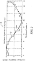
- a graph 50 has a horizontal axis with a scale in units of CVH vertical Hall element position, n, around a CVH sensing element, for example, the CVH sensing element 12 of FIG. 1 .
- the graph 50 also has a vertical axis with a scale in amplitude in units of millivolts.
- the vertical axis is representative of output signal levels from the plurality of vertical Hall elements of the CVH sensing element taken sequentially, one at a time, about the ring of contacts of the CVH sensing element
- the graph 50 includes a signal 52 representative of output signal levels from the plurality of vertical Hall elements of the CVH taken with the magnetic field of FIG. 1 pointing in a direction of forty-five degrees.
- vertical Hall element 0 is centered along the x-axis 20 and vertical Hall element 8 is centered along the y-axis 22.
- the exemplary CVH sensing element 12 there are thirty-two vertical Hall element contacts and a corresponding thirty-two vertical Hall elements, each vertical Hall element having a plurality of vertical Hall element contacts, for example, five contacts. In other embodiments, there are sixty-four vertical Hall element contacts and a corresponding sixty-four vertical Hall elements.
- a maximum positive signal is achieved from a vertical Hall element centered at position 4, which is aligned with the magnetic field 16 of FIG. 1 , such that a line drawn between the vertical Hall element contacts (e.g., five contacts) of the vertical Hall element at position 4 is perpendicular to the magnetic field.
- a maximum negative signal is achieved from a vertical Hall element centered at position 20, which is also aligned with the magnetic field 16 of FIG. 1 , such that a line drawn between the vertical Hall element contacts (e.g., five contacts) of the vertical Hall element at position 20 is also perpendicular to the magnetic field.
- a sine wave 54 is provided to more clearly show ideal behavior of the signal 52.
- the signal 52 has variations due to vertical Hall element offsets, which tend to cause corresponding variations of output signals causing them to be too high or too low relative to the sine wave 54, in accordance with offset errors for each element.
- the offset signal errors are undesirable.
- Groups of contacts of each vertical Hall element can be used in a chopped arrangement (also referred to herein as current spinning) to generate chopped output signals from each vertical Hall element Thereafter, a new group of adjacent vertical Hall element contacts can be selected (i.e., a new vertical Hall element), which can be offset by one element from the prior group. The new group can be used in the chopped arrangement to generate another chopped output signal from the next group, and so on.
- Each step of the signal 52 is representative of an unchopped output signal, i.e., from one respective group of vertical Hall element contacts, i.e., from one respective vertical Hall element.
- each step of the signal 52 can be comprised of several sub-steps (not shown, e.g., four sub-steps), each sub-step indicative of a current spinning "phase.”
- a phase of the signal 52 is related to an angle of the magnetic field 16 of FIG. 1 relative to position zero of the CVH sensing element 12. It will also be understood that a peak amplitude of the signal 52 is generally representative of a strength of the magnetic field 16.
- a phase of the signal 52 e.g., a phase of the signal 54
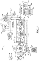
- a magnetic field sensor 100 includes a CVH sensing element 102 having a plurality of vertical Hall elements, each vertical Hall element comprising a group of vertical Hall element contacts (e.g., five vertical Hall element contacts).
- the CVH sensing element 102 can be the same as or similar to the CVH sensing element 12 described above in conjunction with FIG. 1 , and can be disposed proximate to a two pole magnet 144 coupled to a target object 146, which magnet 144 can be the same as or similar to the magnet 14 of FIG. 1 .
- the CVH sensing element 102 can be replaced by a group of magnetic field sensing elements the same as or similar to those described above in conjunction with FIG. 1A .
- the CVH sensing element 102 can be coupled to sequence switches 104 that sequence through the vertical Hall elements of the CVH sensing element 102 to provide an output signal 104a, which can be the same as or similar to the sequenced signal 52 of FIG. 2 .
- the CVH sensing element 102 can also be coupled to current spinning switches 105, which can be coupled to the CVH sensing element 102 via the sequence switches 104.
- Current sources 103 can be configured to generate one or more current signals 103a.
- the current spinning switches 105 can be coupled to receive the one or more current signals 103a and to provide the current signals as signals 104b to the selected vertical Hall elements within the CVH sensing element 102.
- current spinning also referred to as chopping
- current sources e.g., current sources 103
- current sources 103 are sequentially coupled to different selected nodes of a selected vertical Hall element (selected via the sequence switches 104) within the CVH sensing element 102 using the current spinning switches 105.
- the current spinning switches 105 provide couplings to selected output nodes of the selected vertical Hall element in accordance with so-called current spinning phase. Current spinning is further described below in conjunction with FIGS. 4-4D .
- a current spinning sequence selection module 119 can generate a current spinning sequence control signal 119a received by an oscillator and logic module 120.
- the oscillator and logic module 120 can be coupled to provide a control signal 120b to the current spinning switches 105 to control current spinning phase sequences of selected ones of the vertical Hall elements of the CVH sensing element 102.
- the oscillator and logic 120 can also be coupled provide a control signal 120a to the sequence switches 104, to provide sequential selections of the vertical Hall elements within the CVH sensing element 102 and to provide the sequential output signal 104a from the vertical Hall elements of the CVH sensing element 102 in accordance with the selection.
- current spinning is not used.
- a multiplexer 106 can be coupled to receive a signal 105a, with or without current spinning, from the CVH sensing element 102 via the sequences switches 104 and current spinning switches 105.
- the signal 105a can be the same as or similar to the sequential signal 52 of FIG. 2 , or a similar signal that has current spinning, i.e., the above-described sub-steps.
- the multiplexer 106 can also be coupled to receive a clock signal 102c from the oscillator and logic module 120.
- the multiplexer is configured to generate a multiplexed output signal 106a, which, at some times, is representative of the signal 105a, and, at other times, is representative of the clock signal 120c.
- a relative phase between the clock signal 120c and the signal 105a is representative of an angle of the magnetic field generated by the magnet 144 and sensed by the CVH sensing element 102.
- a dual differential amplifier (DDA) 108 can be coupled to receive the multiplexed signal 106a and configured to generate an amplified signal 108a.
- a bandpass filter 110 can be coupled to receive the amplified signal 108a and configured to generate a filtered signal 110a.
- An analog-to-digital converter 112 can be coupled to receive the filtered signal 110a and configured to generate a converted signal 112a, a digital signal.
- An angle calculation module 118 can be coupled to receive the converted signal 112a and configured to generate an uncorrected x-y angle value 118a indicative of the angle of the magnetic field generated by the magnet 144, but with angle error more fully described below.
- the angle calculation module 118 can also be coupled to receive clock signals 120c, 120d from the oscillator and logic module 120.
- the clock signal 120d can be a high speed clock signal.
- the angle calculation module 118 is configured to compare relative phases of the signal 112a, which, at some times, is representative of an amplified and filtered version of the signal 105a, and, at other times, is representative of an amplified and filtered version of the clock signal 120c.
- the uncorrected x-y angle value 118a can have a first angle error component.
- the first angle error component is described more fully below in conjunction with FIG. 5 . Let it suffice here to say that the first angle error component is an angle error component that causes the uncorrected x-y angle value 118a to not be perfectly representative of the true angle of the magnetic field generated by the magnet 144.
- An angle error correction module 138 is coupled to receive the uncorrected x-y angle value 118a and configured to generate an angle error value 138a indicative of the first error component within the uncorrected x-y angle value 118a.
- a combining module 126 here shown to be a summing node, is coupled to receive the uncorrected x-y angle value 118a, coupled to receive the angle error value 138a, and configured to generate a corrected x-y angle value 126a.
- the corrected x-y angle value 126a has a second angle error component that is smaller than the first angle error component of the uncorrected x-y angle value 118a.
- the corrected x-y angle value 126a is more accurately representative of the true angle of the magnetic field generated by the magnet 144.
- the angle correction module 138 is coupled to receive a temperature signal 136a generated by a temperature sensor 136.
- the angle correction module 138 is also coupled to receive sine values, here shown as two sine values 148a, 148b, from a sine look up table (LUT) 148.
- the sine value 148a is representative of a sine value at a fundamental frequency the same as or related to a frequency of the signal 52 of FIG. 2 , i.e., a frequency of the signal 104a and the signal 105a.
- the sine value 148b is representative of a sine value at a second harmonic of the fundamental frequency.
- the sine look up table 148 can provide any number of sine values representative of any number of harmonics of the fundamental frequency. Sine values are described more fully below in conjunction with FIGS. 5 and 6 .
- the sine lookup table 148 can be coupled to receive, and can be indexed in accordance with, the uncorrected x-y angle value 118a and in accordance with so-called interpolated phase values 138b generated by angle error correction module 138. Interpolated phase values are further described below in conjunction with FIG. 6 .
- the magnetic field sensor 100 can be coupled to receive a control signal 142 from outside of the magnetic field sensor 100.
- an electrically erasable programmable read-only memory EEPROM
- EEPROM electrically erasable programmable read-only memory
- the angle correction module 138 is described in greater detail in conjunction with FIG. 6 . However, let it suffice here to say that the angle correction module 138 is configured to use the temperature signal 136a to adjust the angle error value 138a according to the sensed temperature signal 136a.
- the magnetic field sensor 100 can also include a rotation speed module 130 and/or a rotation direction module 132, each coupled to receive the corrected x-y angle value 126a. It will be understood that the corrected x-y angle value 126a can change, and therefore, can be representative of a rotating magnetic field when the magnet 144 rotates.
- the rotation speed module 130 is configured to generate a rotation speed signal or value 130a indicative of a rotation speed of the magnet.
- the rotation direction module 132 is configured to generate a direction signal or value 132a indicative of a rotation direction of the magnet 144.
- An output protocol module 134 is coupled to receive the corrected x-y angle value 126a, the ring rotation speed value 130a, and the rotation direction value 132a.
- the output protocol module 134 is configured to generate an output signal 134a representative of the angle of the magnetic field generated by the magnet 144, representative of the speed of rotation of the magnet 144, and representative of the direction of rotation of the magnet 144.
- the output signal 134a can be provided with the hope one of a variety of conventional formats, for example, an SPI format, a CAN format, anI2C format, or a Manchester format.
- the angle error correction module 138 can be coupled to receive one or more other control signals 150.
- the other control signals 150 are described more fully below in conjunction with FIG. 6 .
- the angle error correction module 138 can make adjustments to the angle error value 138a according to other characteristics of the magnetic field sensor 100.
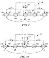
- FIGS. 4-4C are representative of a four phase current spinning or chopping that can be used for a vertical Hall element having five contacts.
- current spinning can be used for each selected vertical Hall element within the CVH sensing element 12 of FIG. 1 and the CVH sensing element 102 of FIG. 3 .
- current spinning can also be used for separate magnetic field sensing elements, for example, the magnetic field sensing elements 30a-30h of FIG. 1A , where the magnetic field sensing elements 30a-30h are selected and chopped one of the time.
- a vertical Hall element 200 of the CVH sensing element 102 of FIG. 3 is comprised of five vertical Hall element contacts, namely, first, second, third, fourth, and fifth vertical Hall element contacts, 202a, 202b, 202c, 202d, 202e, respectively.
- a current source 208 which can be the same as or similar to the current sources 103 of FIG.
- the third vertical Hall element contact 202c is coupled to a voltage reference 210, for example, ground.
- Currents from the current source 208 flow from the first and fifth vertical Hall element contacts 202a, 202e, respectively, through a substrate 206 (e.g., through an epitaxial layer upon a substrate) of the CVH sensing element 200 to the third vertical Hall element contact 202c, as represented by dashed lines.
- the current spinning switches 105 of FIG. 3 can select the second and fourth vertical Hall element contacts 202b, 202d to provide the output signal 105a, and can select the first, fifth, and third vertical Hall element contacts 202a, 202e, 202c, respectively, as those contacts coupled to the current sources 103 of FIG. 3 . Couplings during other current spinning phases described below will be apparent.
- FIG. 4A in which like elements of FIG. 4 are shown having like reference designations, in a second current spinning phase of the same vertical Hall element 200 (same five vertical Hall element contacts) of the CVH sensing element 102, couplings are changed by the current spinning switches 105 of FIG. 3 .
- the current source 208 is coupled to the third vertical Hall element contact 202c, and the first and fifth vertical Hal element contacts 202a, 202e, respectively, are coupled together and to the reference voltage 210.
- the currents flow through the substrate 206 in opposite directions from those shown in FIG. 4 .
- a signal, Vm responsive to an external magnetic field, results between the second and fourth vertical Hall element contacts, 202b, 202d, respectively.
- the signal, Vm, of FIG. 4A is like the signal, Vm, of FIG. 4 .
- the offset voltage within the signals can be different, e.g., different in sign.
- FIG. 4B in which like elements of FIGS. 4 and 4A are shown having like reference designations, in a third current spinning phase upon the same vertical Hall element 200 (same five vertical Hall element contacts) of the CVH sensing element 102), couplings are again changed by the current spinning switches 105.
- the current source 208 is coupled to the second vertical Hall element contact 202b
- the fourth vertical Hall element contact 202d is coupled to the reference voltage 210.
- a current flows from the second vertical Hall element contact 202b through the substrate 206 to the fourth vertical Hall element contact 202d.
- the first and fifth vertical Hall element contacts 202a, 202e, respectively, are coupled together. Some current also flows from the second vertical Hall element contact 202b through the substrate 206 to the first vertical Hall element contact 202a and through the mutual coupling to the fifth vertical Hall element contact 202e. Some current also flows from the fifth vertical Hall element contact 202e through the substrate 206 to the fourth vertical Hall element contact 202d.
- the signal, Vm, of FIG. 4B is like the signal, Vm, of FIGS. 4 and 4A .
- the offset voltage within the signal can be different.
- FIG. 4C in which like elements of FIGS. 4-4B are shown having like reference designations, in a fourth chopping phase upon the same vertical Hall element 200 (same five vertical Hall element contacts) of the CVH sensing element 102, couplings are again changed by the current spinning switches 105.
- the current is reversed from that shown in FIG. 4B .
- the current source 208 is coupled to the fourth vertical Hall element contact 202d, and the second vertical Hall element contact 202b is coupled to the reference voltage 210.
- a current flows from the fourth vertical Hall element contact 202d through the substrate 206 to the second vertical Hall element contact 202b.
- the first and fifth vertical Hall element contacts202a, 202e, respectively, are coupled together. Some current also flows from the fourth vertical Hall element contact 202d through the substrate 206 to the fifth vertical Hall element contact 202e, through the mutual coupling to the first vertical Hall element contact 202a. Some current also flows from the first vertical Hall element contact 202a through the substrate 206 to the second vertical Hall element contact 202b.
- the signal, Vm, of FIG. 4C is like the signal, Vm, of FIGS. 4-4B .
- the offset voltage within the signal can be different.
- the signals, Vm, provided by the four phases of chopping of FIGS. 4-4C are responsive to an external magnetic field.
- the current spinning arrangements of FIGS. 4-4C can move to a next vertical Hall element, e.g., five vertical Hall element contacts offset by one vertical Hall element contact from those shown in FIGS. 4-4C , and the four current spinning phases can be performed on the new vertical Hall element by operation of the current spinning switches 105 of FIG. 3 .
- a sequence of phases (A, B, C, D) represented by the four current spinning phases of FIGS, 4-4C can be changed in one of a variety of ways.
- the sequence of the (A, B, C, D) phases can be randomly selected for each one of the selected vertical Hall elements within the CVH sensing element 102.
- the random selection is fully random, and in some other embodiments, the random selection is a pseudo-random selection.
- the random or pseudo random selection is within each rotation around the CVH sensing element, and in other embodiments, the random or pseudo random selection is among a plurality of rotations around the CVH sensing element.
- the vertical Hall elements within the CVH sensing element 102 can be partitioned into at least two groups or sets of vertical Hall elements, wherein a first set of the vertical Hall elements uses a first sequence of current spinning phases, e.g., ABCD, and a second set of the vertical Hall elements uses a second different sequence of current spinning phases, e.g., CDAB each time the sequence switches 104 sequence around the CVH sensing element 102. There can be one or more vertical Hall elements within each one of the at least two sets of vertical Hall elements.
- phase sequences are also possible, for example, using different phase sequences for any possible number of sets of vertical Hall elements, for example, three, four, five, or more, including twenty-four respective sets of vertical Hall elements, each time the sequence switches 104 sequence around the CVH sensing element 102.
- the above-described different sets of vertical Hall elements receive the above-described randomly or pseudo randomly selected phase sequences selected within each rotation around the CVH sensing element, and in other embodiments, the random or pseudo random selection is among a plurality of rotations around the CVH sensing element.
- a graph 280 has a horizontal axis with a scale in units of angular degrees and a vertical axis with a scale in units of value of an x-y angle value magnitude, for example, a magnitude of the uncorrected x-y angle value 118a of FIG. 3 .
- a line 282 is representative of an x-y angle value that has no angle error.
- the x-y angle value has no angle error, the x-y angle value is perfectly linear with respect to actual angle, i.e., the x-y angle value is a perfect and true representation of the angle of the magnetic field generated by the magnet 144 of FIG. 3 , and the line 282 passes through zero.
- a line 284 is representative of an x-y angle value that has only an average or DC angle error, such that all angles represented by the x-y angle value are offset by a fixed number of degrees.
- the line 284 does not pass through zero.
- a curve 286 is representative of an x-y angle value that has errors in representation of the true angle of the magnetic field generated by the magnet 14, average or DC errors and also an error that has a sinusoidal appearance.
- a curve 288 is representative of an x-y angle value that has other errors in representation of the true angle of the magnetic field generated by the magnet 14.
- a variety of circuit characteristics of the magnetic field sensor 100 contribute to the errors, i.e., to both the DC (or average) angle error represented by the curves 286, 288, and to the sinusoidal shapes of the curves 286, 288.
- One factor that contributes to the errors is switching noise generated by the sequence switches 104 and/or by the current spinning switches 105 of FIG. 3 .
- noise charge injection or switching spikes (together referred to as noise) generated by the sequence switches 104 are not necessarily exactly the same as each sequential vertical Hall element is selected in the CVH sensing element 102.
- a DC (or average) angle error is generated and also a sinusoidal type error such as that represented by the curves 286, 288.
- the sinusoidal error characteristic can be, in part, a result of the noise generated by the sequence switches being repetitive for each cycle around the CVH sensing element 102, and thus, the noise will have an angle error frequency component at a frequency of the signal 52 of FIG. 2 , and will add to the signal 52 (104a of FIG. 3 ).
- the angle error frequency component is essentially fixed in phase relative the signal 104a, and therefore, the addition of the angle error causes different phase shift errors in the summed signal depending on the phase of the signal 104a. Higher harmonics can also result from the noise.
- noise charge injection or switching spikes (together referred to as noise) generated by the current spinning switches 105 are not necessarily exactly the same as each sequential vertical Hall element is selected in the CVH sensing element 102.
- a DC (or average) angle error is generated and also a sinusoidal type error such as that represented by the curves 286, 288.
- the sinusoidal error characteristic can, in part, result from the noise generated by the current spinning switches 105 being repetitive for each cycle around the CVH sensing element.
- phase sequences of the vertical Hall elements within the CVH sensing element 102 can be varied, and thus, the noise generated by the current spinning switches 105 need not be repetitive for each cycle around the CVH sensing element, and corresponding angle error is reduced.
- circuit characteristics including, but not limited to, switching noise and lack of circuit elements settling to final values, tend to be influenced by (i.e., changed by) a variety factors including, but not limited to, temperature of the magnetic field sensor 100 of FIG. 2 , rate of sequencing around the CVH sensing element 102, peak magnitude of the magnetic field experience by the CVH sensing element 102 as the magnet 144 rotates, and selected current spinning sequence(s) among the various vertical Hall elements.
- Differences between the curves 286, 288 can be attributed to changes in the same factors, namely, changes in the temperature, changes in or differences in peak amplitude of the magnetic field experience by the CVH sensing element 102 as the magnet 144 rotates, changes in or differences in rates of sequencing around the CVH sensing element 102, and changes in or differences in selected current spinning sequence(s) among the various vertical Hall elements within the CVH sensing element 102.
- changes in the temperature can occur at any time.
- the changes in the peak amplitude of the magnetic field can be influenced by positional changes, i.e., air gap changes, between the magnet 144 and the CVH sensing element 102 of FIG. 3 .
- the changes in the peak amplitude of the magnetic field can also be influenced by mechanical considerations, for example, wear of a bearing or a shaft upon which the magnet 144 rotates.
- the changes in sequencing rates and the changes in current spinning sequences can be fixed, and changed only for different applications of the magnetic field sensor 100.
- the dominant angle error frequency components occur at first and second harmonics of the frequency of the signal 52 (i.e., 104a or 105a).
- the curves 286, 288 are representative of angle error functions dominated by first and second harmonics of the frequency of the signal 52 (104a).
- the angle error correction module 138 of FIG. 3 is configured to make changes to angle error corrections it applies according to at least the temperature contribution to the angle error represented by the curves 286, 288. In some embodiments, the angle error correction module 138 is also configured to make changes to the angle error corrections according to one or more of the other above-described factors that contribute to the difference between the curves 286, 288.
- angle errors represented by the curves 286, 288 are referred to as first error characteristics, each influenced by the above factors.
- the angle correction module 138 of FIG. 3 can be used to generate the angle error value 138a, which can be used to generate the corrected x-y angle value 126a. Accordingly, other angle error curves (not shown) with lower peak to peak variation than the error curves 286, 288 are representative of second error characteristics that are smaller than the first error characteristics.
- the error curves 286, 288 can be mathematically described in the following way.
- An estimated and quantized angle error (rather than non-quantized error of equation (1)) can be mathematically expressed as: where: q stands for quantized values.
- the angle error correction module 138 of FIG. 3 can use a set of programmable average correction coefficients, programmable amplitude correction coefficients, and programmable phase correction coefficients stored within the EEPROM 140 of FIG. 3 in an expression the same as or similar to the expression of equation (2).
- the misalignment correction coefficient, OFF can also be stored and used.
- the angle error correction module 138 of FIG. 3 can digitally weight, in accordance with the correction coefficients, one or more normalized sine waveforms (values) (i.e., one or more harmonic values) provided by the sine LUT 148, the results of which are summed together in order to approximate the angle error according to equation (2).
- the angle error correction module 138 of FIG. 3 can generate the angle error value 138a according to equation (2).
- the error correction module 138 evaluates equation (2) using two harmonics, first and second. In some other embodiments, the error correction module 138 evaluates equation (2) with one harmonic, first or second. In some other embodiments, the error connection module 138 evaluates equation (2) with more than two harmonics, for example, first, second, third, fourth, and fifth harmonics. In some other embodiments, the error correction module 138 evaluates equation (2) also using also the average value, DC q ( T ). In some other embodiments, the error correction module 138 evaluates equation (2) using only the average value, DC q ( T ), without any sine functions or harmonics, and with or without the misalignment correction coefficient, OFF. In some embodiments, the error correction module 138 evaluates an equation different from equation (2), but having correction coefficients that can be stored in the coefficient table EEPROM 310.
- the combining module 126 is operable to combine the angle error value (i.e., the estimated error according to equation (2)), which is temperature dependent, with the uncorrected x-y angle value 118a.
- the estimated error, ⁇ ' err for measured angle ⁇ according to equation (2) can be digitally subtracted from (or added to) the sensed (i.e., measured) angle, ⁇ , (i.e., the uncorrected x-y angle value 118a of FIG. 2 ), which contains an error represented by the curves 286, 288 of FIG. 5 .
- each harmonic component of the angle error represented by equation (2) can change independently in amplitude and phase.
- angle error variations as a function of temperature of each parameter are approximated between pairs of stored average, amplitude, and phase values using a piecewise-linear interpolation.
- Variation in current spinning phase sequences is described above in conjunction with FIG. 3 .
- An angle error correction module is also described above in conjunction with FIGS. 3 and 5 . It should be apparent that both a proper selection of the variation of the current spinning phase sequences and the use of the angle error correction module tend to reduce a magnitude of the angle error represented by the curves 286, 288. It should be appreciated that the two techniques can be used separately or together to achieve a reduction in angle error of the magnetic field sensor 100.
- the angle error correction module 138 can coupled to a coefficient table EEPROM 310.
- the coefficient table EEPROM 310 is configured to store a plurality of correction coefficients of values associated with the above equation (2), and associated with so-called temperature segments.
- the coefficient table EEPROM 310 can be part of the EEPROM 140 of FIG. 3 .
- the term "temperature segment” is used to describe one of a plurality of temperature ranges, each temperature range bounded by a pair of temperatures. Examples shown herein and described below use four such temperature segments, a first temperature segment adjacent to the second temperature segment, the second temperature segment adjacent to a third temperature segment, and a fourth temperature segment adjacent to the third temperature segment, in ascending order of temperatures, In some embodiments the temperature segments overlap, and, in other embodiments, there are temperature spaces between the temperature segments. In some embodiments, each temperature segment spans the same number of degrees of temperature, and in other embodiments the temperature segments span different numbers of degrees of temperature. For example, in some embodiments the second and third temperature segments can each have wider temperature span than the first and fourth segments.
- the coefficient table EEPROM 310 can store therein a plurality of temperature values, e.g., T0, T1, T2, T3, T4, T5, representative of boundaries of four temperature segments.
- the coefficient table EEPROM 310 can also store therein a plurality of correction coefficients.
- the coefficient table EEPROM 310 can store five average correction coefficients, Coeff A0, Coeff A1, Coeff A2, Coeff A3, Coeff A4.
- Each of the five average correction coefficients is representative of an average value, DC q ( T ), in equation (2), at a different respective temperature corresponding to temperatures at the boundaries of the four temperature segments.
- the coefficient table EEPROM 310 can also store five first harmonic amplitude correction coefficients, Coeff B0, Coeff B1, Coeff B2, Coeff B3, Coeff B4.
- the coefficient table EEPROM 310 can also store five first harmonic phase correction coefficients, Coeff C0, Coeff C1, Coeff C2, Coeff C3, Coeff C4.
- the coefficient table EEPROM 310 can also store five second harmonic amplitude correction coefficients, Coeff D0, Coeff D1, Coeff D2, Coeff D3, Coeff D4.
- the coefficient table EEPROM 310 can also store five second harmonic phase correction coefficients, Cooff E0, Coeff E1, Coeff E2, Coeff E3, Coeff E4.
- the coefficient table EEPROM 310 can also store the misalignment correction coefficient, OFF, (not shown) representative of the above described mechanical misalignment of the CVH sensing element 102 with the magnetic field generated by the magnet 144 of FIG. 3 .
- all of the stored correction coefficients and values can be programmed into the coefficient table EEPROM 310, for example, by way of the control signal 142.
- the angle error correction module 138 can include an analog-to-digital converter 300 coupled to receive the temperature signal 136a from the temperature sensor 136.
- the analog-to-digital converter 300 is configured to generate a converted signal 300a, which is a digital signal representative of the temperature of the magnetic field sensor 100.
- the angle error correction module 138 includes a segment identification module 302 coupled to receive the digital temperature signal 300a and configured to identify one of a plurality of temperature segments in which the digital temperature signal 300a lies.
- the segment identification module 302 can receive information 310a about the stored temperature segments, e.g., temperature boundaries T0, T1, T2, T3, T4, T5 of four stored four temperature segments, from the coefficient table EEPROM 310.
- the segment identification module 302 is operable to identify between which two adjacent temperatures the digital temperature signal 300a lies, i.e., within which one of the four temperature segments the digital temperature signal 300a lies.
- the segment identification module is operable to generate a segment identifier signal 302b representative of the identified temperature segment.
- the angle error correction module 138 also includes an interpolation module 304 coupled to receive the digital temperature signal 300a and coupled to receive the segment identifier signal 302b.
- the interpolation module 304 is also coupled to receive identified coefficients 310b, identified by the segment identification module 302.
- the interpolation module is configured to generate a correction coefficient request signal 304b received by the coefficient table EEPROM 310.
- the coefficient table EEPROM provides a plurality of correction coefficients 310b associated with the temperature boundaries of the identified temperature segment. It will be understood that identification of the temperature segment results in selection of ten correction coefficients, five correction coefficients at the temperature of each one of the boundaries of the identified temperature sites.
- the interpolation module 304 is operable to interpolate between pairs of the identified and received correction coefficients 310b. For example, if the digital temperature signal 300a is representative of a temperature of two hundred fifty degrees, and if the pair of average value correction coefficients, e.g., Coeff A2, Coeff A3 are correction coefficients associated with a temperature segment spanning from two hundred degrees to three hundred degrees (i.e., a third temperature segment in which the digital temperature signal 300a lies), then it should be apparent that the interpolation module can interpolate between the two correction coefficients, Coeff A2, Coeff A3, to arrive at an interpolated correction coefficient. Similar interpolations can be performed by the interpolation module 304 between other ones of the pairs of correction coefficients associated with the third temperature segment to generate a plurality of interpolated correction coefficients 304a
- the interpolation module 304 can perform linear interpolations. In other embodiments the interpolation module 314 can perform nonlinear interpolations. In some embodiments, the interpolation module 304 can perform a type of interpolation appropriate for a width of a temperature segment For example, if a width of the identified temperature segment is relatively wide, then the interpolation module 304 can perform a linear interpolation where the digital temperature signal 300a falls within that wide temperature segment. Conversely, if a width of the identified temperature segment is narrow, which may be indicative of a rapidly changing error characteristic, and the interpolation module 304 can perform a nonlinear interpolation where the digital temperature signal 300a falls within that narrower temperatures segment.
- the angle error correction module 138 includes an algorithm module 306 coupled to receive the interpolated correction coefficients 304a and configured to use the interpolated correction coefficients 304a in an algorithm, for example, an algorithm that uses equation (2) above.
- the algorithm module 306 can employ equation (2) with any number of harmonics and with or without the average or DC correction coefficients.
- the algorithm module 306 is configured to generate an x-y angle error value 306a.
- the x-y angle error value 306a bypasses an optional combining module 313, and becomes the x-y angle error value 138a described above in conjunction with FIG. 3 .
- a combining module 126 is coupled to receive the x-y angle error value 138a, coupled to receive the uncorrected x-y angle value 124a, and configured to combine the two values to generate the corrected x-y angle value 126a that is more accurate and has a smaller (i.e., a second) error component smaller than the first error component of the uncorrected x-y angle value 124a.
- the sine look up table 148 is described above in conjunction with FIG. 3 .
- the sine lookup table 148 can provide first and second harmonics sine values 148a, 148b, respectively, to the algorithm module 306 for use in evaluating equation (2) above.
- a sine lookup controller 318 can be coupled to receive the uncorrected x-y angle value 124a, and coupled to receive interpolated phase values 304b from the interpolation module. It will be apparent from equation (2) that both of these values are required in order to know how to index into the sine lookup table 148.
- the parameter sin (na + H nP_q ( T )) of equation (2) requires an index including both the measured (i.e., uncorrected) angle, ⁇ , and an interpolated phase, H nP_q ( T ). Recall that the parameter n is a harmonic number.
- the angle error correction module 138 can optionally include a temperature change detection module 315 coupled to receive the digital temperature signal 300a and configured to identify if the digital temperature signal 300a is representative of a change in temperature or representative of no change temperature.
- the temperature change detection module can be configured to generate a control signal 315a also indicative of a change in temperature or indicative of no change in temperature.
- the interpolation module 304 can perform the above described interpolations and provide new interpolated correction coefficients 304a only when the control signal 315a is indicative of a change in temperature. At other times, the algorithm module can use interpolated correction coefficients that were previously calculated.
- the angle error correction module 138 can include one or more of a correction versus current spinning sequence module 311, a correction versus magnetic field amplitude module 309, or a correction versus sequence rate module 307.
- the correction versus current spinning sequence module 311 is configured to identify a correction factor related to the selected sequence of current spinning phase sequence groups that can be applied to further improve the x-y angle error value 138a.
- the correction versus magnetic field amplitude module 309 is configured to identify a correction factor related to the amplitude of the magnetic field experience by the CVH sensing element 102 and can be applied to further improve the x-y angle error value 138a.
- the correction versus sequence rate module 307 is configured to identify a correction factor related to the rate at which a vertical Hall elements within the CVH sensing element 102 of FIG. 3 are sequenced, which correction factor can be applied to further improve the x-y angle error value 138a.
- a correction value 307a includes one or more of the above correction factors.
- the correction value 307a can be received by a combining module 313, and can be applied to the x-y angle error value 306a, so that the corrected x-y angle value 126a will have a third error component, which is smaller than the above-described first and second error components. In other words, the corrected x-y angle value 126a is still more truly representative of an actual angle.
- a program control EEPROM 308 can be coupled to receive the control signal 142.
- the program control EEPROM 308 can be coupled to one or more of the interpolation module 304 or the algorithm module 306.
- a user can program the magnetic field sensor 100 of FIG. 3 to use a selected type of interpolation within the interpolation module.
- a user can program the magnetic field sensor 100 of FIG. 3 to use a selected type of algorithm within the algorithm module 306.
- the magnetic field sensor 100 uses equation (2) as the algorithm, and in other embodiments, the magnetic field sensor uses a different algorithm.
- FIGS. 7-9 show the advantages of similar current spinning phase sequence variations applied to a simple planar Hall Effect element, by way of an example useful for understanding the invention.
- a simple magnetic field sensor 400 includes a planar Hall Effect element 402.
- the Hall element 402 is coupled to receive a current signal 412a at different selected ones of four contacts in accordance with a plurality of current spinning phases determined by current spinning switches 412.
- a current source 410 supplies a current signal 410a to the current spinning switches 412.
- a differential output 402a, 402b of the Hall effect element 402 is coupled to current spinning switches 404, which select different ones of the four terminals as the output terminals as current spinning progresses through the plurality of phases.
- the magnetic field sensor 400 can include a current spinning and filter control module 408 coupled to the current spinning switches 404, 412, which can be configured to vary or change the sequence of phases from time to time or upon each cycle through a set of four phases.
- the variations can be fully random or pseudo-random. However, in other arrangements the variations can select between two or more current spinning phase sequences from time to time.
- current spinning phases can take on the following four sequences and then repeat: ABCD, BCDA, CDAB, DABC.
- ABCD ABCD
- BCDA CDAB
- DABC current spinning phase sequences
- only four current spinning phase sequences are used, each having four phases.
- four current spinning phases can result in twenty-four combinations of the four phases in twenty-four current spinning phase sequences.
- the twenty-four current spinning phase sequences can be randomly selected, pseudo-randomly selected, or periodically selected.
- the current spinning phase sequence applied to the Hall element 402 can be changed from time to time between the two phase sequences.
- the current spinning switches 404 are configured to provide a differential output signal 404a, 404b.
- a filter 406 is coupled to receive the differential signal from the current spinning switches 404 and is configured to provide a differential output signal 406a, 406b.
- the differential signal 404a, 404b appearing at the current spinning switches has two frequency components.
- a baseband component is responsive to a magnetic field and remains at baseband.
- an offset signal component with the differential signal 404a, 404b is shifted to a higher frequency according to a frequency at which the current spinning sequences through the phases, i.e., a chopping frequency.
- the filter 406 can remove the offset signal component of the differential signal 404a, 404b, leaving only the magnetically responsive signal component in the differential output signal 406a, 406b.
- a graph 450 has a horizontal axis with a scale in units of frequency in arbitrary units and a vertical axis with a scale in amplitude in arbitrary units.
- the graph 450 is representative of operation of a magnetic field sensor like the magnetic field sensor 400 of FIG. 7 , but without any variation of the current spinning phase sequences applied to the Hall element 402.
- the phase sequence ABCD repeats over and over without variation.
- a spectral line 454 is representative of the magnetically responsive signal component of the differential signal 404a, 404b of FIG. 7 .
- a spectral line 458 is representative of the offset signal component of the differential signal 404a, 404b of FIG. 7 after the current spinning operation of the current spinning switches 404, 412, but without variation of the current spinning phase sequences.
- a spectral line 460 is representative of a third harmonic of the offset signal component represented by the spectral line 456.
- spectral line 454 is representative of the magnetic field sensing element 402 being responsive to a DC magnetic field.
- the magnetic field sensing element 402 can be responsive to AC magnetic fields.
- a baseband bandwidth 456 is representative of a region in which the magnetic field sensing element 402 can provide signal information responsive to a magnetic field.
- a transfer function 452 is representative of a transfer function of one of particular example of the filter 406 of FIG. 7 .
- the transfer function 452 is representative of a digital filter having transfer function notches.
- the differential output signal 406a, 406b will have content only within the baseband 456.
- a graph 500 has a horizontal axis with a scale in units of frequency in arbitrary units and a vertical axis with a scale in amplitude in arbitrary units.
- the graph 500 is representative of operation of a magnetic field sensor like the magnetic field sensor 400, including variations or changes of the current spinning phase sequences. It will become apparent from discussion below that, using variation of the current spinning phase sequences, in some examples, the filter 406 of FIG. 7 can be eliminated.
- a spectral line 502 is representative of the magnetically responsive signal component of the differential signal 404a, 404b.
- a spectral line 506 is representative of the offset signal component of the differential signal 404a, 404b after the varied current spinning operation of the current spinning switches 404, 412.
- a spectral line 508 is representative of a third harmonic of the offset signal component represented by the spectral line 506.
- spectral line 502 is representative of the magnetic field sensing element 402 being responsive to a DC magnetic field.
- the magnetic field sensing element 402 can be responsive to an AC magnetic field.
- a baseband bandwidth 504 is representative of a region in which the magnetic field sensing element 402 can provide signal information responsive to a magnetic field.
- the spectral lines 506, 508, and all other extraneous spectral lines have a much lower amplitude than the spectral lines 458, 460 of FIG. 8 .
- the various low amplitude spectral lines have a low enough amplitude that the filter 406 of FIG. 7 is not required in all. Having no filter at all results in a faster magnetic field sensing element and a wider bandwidth magnetic field sensing element.
- the baseband passband 504 can be substantially wider than that shown, and can be wider than the baseband passband 456 of FIG. 8 . In some examples, the baseband passband 504 can extend well beyond the frequency 3fc.
Landscapes
- Physics & Mathematics (AREA)
- General Physics & Mathematics (AREA)
- Condensed Matter Physics & Semiconductors (AREA)
- Health & Medical Sciences (AREA)
- Engineering & Computer Science (AREA)
- Environmental & Geological Engineering (AREA)
- Toxicology (AREA)
- Transmission And Conversion Of Sensor Element Output (AREA)
- Measuring Magnetic Variables (AREA)
Description
- This invention relates generally to magnetic field sensors and, more particularly, to a magnetic field sensor that can provide an output signal representative of an angle of rotation of a target object, for which angular errors are reduced.
- Magnetic field sensing elements can be used in a variety of applications. In one application, a magnetic field sensing element can be used to detect a direction of a magnetic field, i.e., and angle of the direction of the magnetic field.
- Planar Hall elements and vertical Hall elements are known types of magnetic field sensing elements. A planar Hall element tends to be responsive to magnetic field perpendicular to a surface of a substrate on which the planar Hall element is formed. A vertical Hall element tends to be responsive to magnetic field parallel to a surface of a substrate on which the vertical Hall element is formed.
- Other types of magnetic field sensing elements are known. For example, a so-called "circular vertical Hall" (CVH) sensing element, which includes a plurality of vertical Hall elements, is known and described in PCT Patent Application No.
PCT/EP2008/056517 PCT Publication No. WO 2008/145662 . The CVH sensing element is a circular arrangement of vertical Hall elements arranged over a common circular implant and diffusion region in a substrate. The common implant and diffusion region can be a common epi (epitaxial) region (e.g., layer) upon a substrate, bounded by semiconductor isolation structures. The CVH sensing element can be used to sense a direction (i.e., an angle) (and optionally a strength) of a magnetic field in a plane of the substrate. - Various parameters characterize the performance of magnetic field sensing elements and magnetic field sensors that use magnetic field sensing elements. These parameters include sensitivity, which is a change in an output signal of a magnetic field sensing element in response to a change of magnetic field experienced by the magnetic sensing element, and linearity, which is a degree to which the output signal of the magnetic field sensing element varies in direct proportion to the magnetic field. These parameters also include an offset, which is characterized by an output signal from the magnetic field sensing element not representative of a zero magnetic field when the magnetic field sensing element experiences a zero magnetic field.
- The above-described CVH sensing element is operable, with associated circuits, to provide an output signal representative of an angle of a direction of a magnetic field. Therefore, as described below, if a magnet is disposed upon or otherwise coupled to a so-called "target object," for example, a camshaft in an engine, the CVH sensing element can be used to provide an output signal representative of an angle of rotation of the target object.
- The CVH sensing element is but one element that can provide an output signal representative of an angle of a magnetic field, i.e., an angle sensor. For example, an angle sensor can be provided from a plurality of separate vertical Hall elements or a plurality of magnetoresistance elements. Collectively, magnetic field sensing element(s) that generate an output signal related to an angle of a magnetic field are referred to herein "angle sensing elements."
- More parameters can characterize the performance of and angle sensing element(s), e.g., a CVH sensing element One such parameter is an angular accuracy of the output signal generated by the angle sensing elements). Angular accuracy can have both an average angle error that is the same at all magnetic field pointing angles, and also an angle error that is different at different magnetic field angles (i.e. a non-linearity error). Another parameter is the speed with which the angle sensing element(s) can convey the angle of the magnetic field. It will be understood that the speed is particularly important for applications in which the angle of the magnetic field may be rapidly changing.
- It is know that some parameters that can characterize an angle sensing element tend to change with temperature.
-
US 2005/278137 A1 discloses a method for adjusting a determination rule for an error compensation of an angle sensor, which is designed to detect a first component of a direction along a first axis and a second component of a direction along a second axis, and to determine an angle of the direction according to the determination rule based on the first and second components. The method includes: detecting values of component pairs consisting of two predetermined components for the calculation of offset and/or amplitude and/or axis-angle errors. -
US 2012/095712 A1 discloses an angle detection unit including first to third arithmetic units which receives first and second signals that are associated with intensities of components of a rotating magnetic field in mutually different directions. The first arithmetic unit generates a sum of squares signal made up of the sum of squares of the first and second signals. Based on the sum of squares signal, the second arithmetic unit calculates a first error component estimate which is an estimated value of a first error component included in the first signal and a second error component estimate which is an estimated value of a second error component included in the second signal. The third arithmetic unit generates a first corrected signal by subtracting the first error component estimate from the first signal, generates a second corrected signal by subtracting the second error component estimate from the second signal, and calculates a detected angle value based on the first and second corrected signals. -
WO 98/02721 A2 -
US 2012/086442 A1 discloses a magnetic field sensor and a method associated with the magnetic field sensor, which provide gain correction coefficients and/or offset correction coefficients stored in the magnetic field sensor in digital form. The gain correction coefficients and/or offset correction coefficients can be used to generate analog control signals to control a sensitivity and/or an offset of an analog signal path through the magnetic field sensor. - Other arrangements of magnetic field sensors are disclosed in
US 4327416 A ,DE 10 2005 024879 A1US 2012/262155 A1 . - It would be desirable to provide circuits and techniques that can process output signals from an angle sensing element to provide an output signal that has a high degree of angle accuracy and a relatively high speed.
- The present invention provides circuits and techniques that can process output signals from an angle sensing element to provide an output signal that has a high degree of angle accuracy and a relatively high speed.
- In accordance with one aspect, a magnetic field sensor includes a plurality of magnetic field sensing elements, each one of the plurality of magnetic field sensing elements is configured to generate a respective x-y output signal responsive to a magnetic field in an x-y plane. The magnetic field sensor also includes an angle processing circuit coupled to receive the x-y output signals and configured to generate an uncorrected x-y angle value representative of an angle of the magnetic field in an x-y plane. The uncorrected x-y angle value has a first angle error component. The magnetic field sensor also includes an angle error correction module coupled to the angle processing circuit and configured to generate an x-y angle error value indicative of an error in the uncorrected x-y angle value. The magnetic field sensor also includes a combining module configured to combine the uncorrected x-y angle value with the x-y angle error value to generate a corrected x-y angle value having a second angle error component smaller than the first angle error component.
- The above magnetic field sensor further includes:
- a coefficient table memory configured to store a plurality of correction coefficients, associated with respective boundaries of a plurality of temperature segments, each temperature segment bounded by a pair of temperatures; and
- a temperature sensor configured to generate a temperature signal representative of a temperature; wherein the angle error correction module comprises:
- a segment identification module coupled to receive a temperature value representative of the temperature signal and configured to identify a temperature segment in which the temperature value falls;
- an interpolation module coupled to receive a plurality of the correction coefficients associated with the identified temperature segment, coupled to receive the temperature value, and configured to interpolate between pairs of the correction coefficients in accordance with the temperature value to generate a plurality of interpolated correction coefficients; and
- an algorithm module coupled to receive the plurality of interpolated correction coefficients and configured to apply an algorithm using the plurality of interpolated correction coefficients to generate an x-y angle error value.
- The above magnetic field sensor further Includes a sine lookup table for storing a plurality of sine values, wherein the algorithm module is coupled to receive a sine value selected from among the plurality of sine values and to apply the algorithm also using the selected sine value.
- In some embodiments, the above magnetic field sensor can Include one or more of the following aspects, in any combination.
- In some embodiments of the above magnetic field sensor, the plurality of magnetic field sensing elements comprises a plurality of vertical Hall Effect elements arranged as a circular vertical Hall (CVH) element, wherein each one of the plurality of vertical Hall Effect elements is arranged upon a common circular implant and diffusion region in a first major surface of a semiconductor substrate, wherein the plurality of vertical Hall Effect elements is configured to generate a respective plurality of x-y output signals responsive to a magnetic field having a direction component in an x-y plane parallel to the first surface of the semiconductor substrate, the x-y plane having an x-direction and a y-direction orthogonal to the x-direction, wherein the plurality of x-y output signals is generated in a plurality of cycle periods, each cycle period corresponding to one cycle around the CVH sensing element, the cycle periods occurring at a cycle rate.
- In some embodiments of the above magnetic field sensor, the selected sine value is selected in accordance with the uncorrected x-y angle value.
- In some embodiments of the above magnetic field sensor, the selected sine value is selected in accordance with the x-y angle value and in accordance with an interpolated phase coefficient.
- In some embodiments of the above magnetic field sensor, the angle error correction module is configured to use a temperature-dependent sinusoidal error relationship to describe the first angle error component, sinusoidal with respect to the angle of the magnetic field, and wherein the plurality of correction coefficients comprises:
a plurality of correction coefficients representative of respective magnitudes and phases of one or more harmonics of the sinusoidal error relationship at a corresponding plurality of different temperatures. - In some embodiments of the above magnetic field sensor, the plurality of correction coefficients further comprises a plurality of correction coefficients representative of respective magnitudes and phases of first and second harmonics of the sinusoidal error relationship at a corresponding plurality of different temperatures.
- In some embodiments of the above magnetic field sensor, the plurality of correction coefficients further comprises a plurality of correction coefficients representative of respective magnitudes of average angle errors of the sinusoidal error relationship at a corresponding plurality of different temperatures.
- In some embodiments, the above magnetic field sensor further includes a program control register coupled to receive a program control value, wherein the interpolation module is coupled to receive a value representative of the program control value, and, in response to the program control value, the interpolation module is configured to select the sinusoidal error relationship from among a plurality of sinusoidal error relationships.
- In some embodiments, the above magnetic field sensor further includes a program control register coupled to receive a program control value, wherein the interpolation module is coupled to receive a value representative of the program control value, and, in response to the program control value, the interpolation module is configured to select an interpolation type from among a plurality of interpolation types.
- In some embodiments of the above magnetic field sensor, the interpolation module is configured to generate linear interpolations.
- In some embodiments of the above magnetic field sensor, the interpolation module is configured to generate non-linear interpolations.
- In some embodiments of the above magnetic field sensor, boundaries of the plurality of temperature segments are unequally spaced in temperature.
- In some embodiments, the above magnetic field sensor further includes:
a temperature change detection module coupled to the temperature sensor and configured to detect a change in temperature and to generate a temperature change signal indicative of a change in temperature or indicative of no change in temperature, wherein the interpolation module is coupled to the temperature change module and configured to change the plurality of interpolated correction coefficients when the temperature change signal is indicative of a change in temperature and to hold the plurality of interpolated correction coefficients when the temperature change signal is indicative of no change in temperature. - In some embodiments, the above magnetic field sensor further includes:
- a correction versus rate module coupled to receive a control signal related to the cycle rate and configured to generate a cycle rate correction value in accordance with the cycle rate; and
- a second combining module configured to combine the cycle rate correction value with the x-y angle error value to generate a further corrected x-y angle value comprising a third angle error component smaller than the second angle error component.
- In some embodiments, the above magnetic field sensor further includes:
- a correction versus current spin sequence module coupled to receive a control signal related to a current spin sequence of the CVH sensing element and configured to generate a current spin sequence correction value in accordance with the current spin sequence; and
- a second combining module configured to combine the current spin sequence correction value with the angle error value to generate a further corrected x-y angle value comprising a third angle error component smaller than the second angle error component.
- In some embodiments, the above magnetic field sensor further includes:
- a correction versus magnetic field strength module coupled to receive a control signal related to a magnitude of the magnetic field and configured to generate a magnetic field strength correction value in accordance with the magnitude of the magnetic field; and
- a second combining module configured to combine the magnetic field strength correction value with the angle error value to generate a further corrected x-y angle value comprising a third angle error component smaller than the second angle error component
- In accordance with another aspect, a method of reducing an error in a magnetic field sensor includes providing a plurality of magnetic field sensing elements. Each one of the plurality of magnetic field sensing elements is configured to generate a respective x-y output signal responsive to a magnetic field in an x-y plane. The method also includes using the x-y output signals to generate an uncorrected x-y angle value representative of an angle of the magnetic field in an x-y plane. The uncorrected x-y angle value comprises a first angle error component. The method includes generating an x-y angle error value indicative of an error In the uncorrected x-y angle value.
- The method also includes correcting the uncorrected x-y angle value to provide a corrected x-y angle value having a second angle error component smaller than the first angle error component, wherein the correcting the uncorrected x-y angle value comprises:
- storing a plurality of correction coefficients associated with respective boundaries of a plurality of temperature segments, each temperature segment bounded by a pair of temperatures;
- generating a temperature signal representative of a temperature;
- identifying a temperature segment in which the temperature value falls;
- interpolating between pairs of the correction coefficients in accordance with the temperature value to generate a plurality of interpolated correction coefficients; and
- applying an algorithm using the plurality of interpolated correction coefficients to generate an x-y angle error value, wherein the combining comprises:
combining the uncorrected x-y angle value with the x-y angle error value to generate the corrected x-y angle value, wherein the method further includes storing a plurality of sine values, wherein applying the algorithm further comprises: selecting a sine value from among the plurality of sine values; and applying the algorithm using the selected sine value. - In some embodiments of the above method, the plurality of magnetic field sensing elements comprises a plurality of vertical Hall Effect elements arranged as a circular vertical Hall (CVH) element, wherein each one of the plurality of vertical Hall Effect elements is arranged upon a common circular implant and diffusion region in a first major surface of a semiconductor substrate, wherein the plurality of vertical Hall Effect elements is configured to generate a respective plurality of x-y output signals responsive to a magnetic field having a direction component in an x-y plane parallel to the first surface of the semiconductor substrate, the x-y plane having an x-direction and a y-direction orthogonal to the x-direction, wherein the plurality of x-y output signals is generated in a plurality of cycle periods, each cycle period corresponding to one cycle around the CVH sensing element, the cycle periods occurring at a cycle rate.
- In some embodiments of the above method, the selected sine value is selected in accordance with the uncorrected x-y angle value.
- In some embodiments of the above method, the selected sine value is selected in accordance with the uncorrected x-y angle value and in accordance with an interpolated phase coefficient
- In some embodiments of the above method, the applying the algorithm comprises:
- using a temperature dependent sinusoidal error relationship to describe the first angle error component, sinusoidal with respect to the angle of the magnetic field, and wherein the plurality of correction coefficients comprises;
- a plurality of correction coefficients representative of respective magnitudes and phases of one or more harmonics of the sinusoidal error relationship at a corresponding plurality of different temperatures.
- In some embodiments of the above method, the plurality of correction coefficients further comprises a plurality of correction coefficients representative of respective magnitudes and phases of first and second harmonics of the sinusoidal error relationship at a corresponding plurality of different temperatures.
- In some embodiments of the above method, the plurality of correction coefficients further comprises a plurality of correction coefficients representative of respective magnitudes of average angle errors of the sinusoidal error relationship at a corresponding plurality of different temperatures.
- In some embodiments, the above method further includes:
- receiving a program control value; and
- selecting the sinusoidal error relationship from among a plurality of sinusoidal error relationships.
- In some embodiments, the above method further includes:
- receiving a program control value; and
- selecting an interpolation type from among a plurality of interpolation types.
- In some embodiments of the above method, the interpolation module is configured to generate linear interpolations.
- In some embodiments of the above method, the interpolation module is configured to generate non-linear interpolations
- In some embodiments of the above method, boundaries of the plurality of temperature segments are unequally spaced in temperature.
- In some embodiments, the above method further includes:
- detecting a change in temperature;
- generating a temperature change signal indicative of a change in temperature or indicative of no change in temperature; and
- changing the plurality of interpolated correction coefficients when the temperature change signal is indicative of a change in temperature and holding the plurality of interpolated correction coefficients when the temperature change signal is indicative of no change in temperature.
- In some embodiments, the above method further includes:
- generating a cycle rate correction value in accordance with the cycle rate; and
- combining the cycle rate correction value with the angle error value and with the uncorrected angle value to generate a further corrected x-y angle value comprising a third angle error component smaller than the second angle error component.
- In some embodiments, the above method further includes:
- generating a current spin sequence correction value in accordance with the current spin sequence; and
- combining the current spin sequence correction value with the angle error value to generate a further corrected x-y angle value comprising a third angle error component smaller than the second angle error component.
- In some embodiments, the above method further includes:
- generating a magnetic field strength correction value in accordance with the magnitude of the magnetic field; and
- combining the magnetic field strength correction value with the angle error value to generate a further corrected x-y angle value comprising a third angle error component smaller than the second angle error component
- The foregoing features of the invention, as well as the invention itself may be more fully understood from the following detailed description of the drawings, in which:
-
FIG. 1 is a pictorial showing a circular vertical Hall (CVH) sensing element having a plurality of vertical Hall elements arranged in a circle over a common implant region upon a substrate, and a two pole magnet disposed close to the CVH sensing element; -
FIG. 1A is pictorial showing a plurality of magnetic field sensing elements; -
FIG. 2 is a graph showing an output signal as may be generated by the CVH sensing element ofFIG. 1 or by the plurality of magnetic field sensing elements ofFIG. 1A ; -
FIG. 3 is a block diagram of an exemplary magnetic field sensor having a CVH sensing element, having a current spinning sequence selection module configured to provide current spinning of vertical Hall elements within the CVH sensing element with variations of current spinning phase sequences, and also having an angle error correction module configured to estimate an angle error value that can be applied to reduce an angular error; -
FIGS. 4-4C are block diagrams showing a vertical Hall element of the CVH sensing element ofFIG. 3 when coupled into four current spinning phases, each phase associated with operation of one of the vertical Hall elements of the CVH sensing element ofFIG. 3 ; -
FIG. 5 is a graph showing ideal and non-ideal operation of the magnetic field sensor ofFIG. 3 ; -
FIG. 6 is a block diagram showing further details of the angle error correction module ofFIG. 3 ; -
FIG. 7 is a block diagram of a magnetic field sensor that has but one planar Hall element, and that has a current spinning/filter control module to control current spinning phases; -
FIG. 8 is a graph showing a frequency domain of operation of the magnetic field sensor ofFIG. 7 , when operated in a with repeating current spinning phase sequences; and -
FIG. 9 is a graph showing a frequency domain of operation of the magnetic field sensor ofFIG. 7 when operated with varying current spinning phase sequences. - As used herein, the term "magnetic field sensing element" is used to describe a variety of electronic elements that can sense a magnetic field The magnetic field sensing element can be, but is not limited to, a Hall Effect element, a magnetoresistance element, or a magnetotransistor. As is known, there are different types of Hall Effect elements, for example, a planar Hall element, a vertical Hall element, and a circular vertical Hall (CVH) element. As is also known, there are different types of magnetoresistance elements, for example, a semiconductor magnetoresistance element such as Indium Antimonide (InSb), a giant magnetoresistance (GMR) element, an anisotropic magnetoresistance element (AMR), a tunneling magnetoresistance (TMR) element, and a magnetic tunnel junction (MTJ). The magnetic field sensing element may be a single element or, alternatively, may include two or more magnetic field sensing elements arranged in various configurations, e.g., a half bridge or full (Wheatstone) bridge. Depending on the device type and other application requirements, the magnetic field sensing element may be a device made of a type IV semiconductor material such as Silicon (Si) or Germanium (Ge), or a compound, e.g., type III-V, semiconductor material like Gallium-Arsenide (GaAs) or an Indium compound, e.g., Indium-Antimonide (InSb).
- As is known, some of the above-described magnetic field sensing elements tend to have an axis of maximum sensitivity parallel to a substrate that supports the magnetic field sensing element, and others of the above-described magnetic field sensing elements tend to have an axis of maximum sensitivity perpendicular to a substrate that supports the magnetic field sensing element. In particular, planar Hall elements tend to have axes of sensitivity perpendicular to a substrate, while metal based or metallic magnetoresistance elements (e.g., GMR, TMR, AMR) and vertical Hall elements tend to have axes of sensitivity parallel to a substrate.
- As used herein, the term "magnetic field sensor" is used to describe a circuit that uses a magnetic field sensing element, generally in combination with other circuits. Magnetic field sensors are used in a variety of applications, including, but not limited to, an angle sensor that senses an angle of a direction of a magnetic field, a current sensor that senses a magnetic field generated by a current carried by a current-carrying conductor, a magnetic switch that senses the proximity of a ferromagnetic object, a rotation detector that senses passing ferromagnetic articles, for example, magnetic domains of a ring magnet or a ferromagnetic target (e.g., gear teeth) where the magnetic field sensor is used in combination with a back-biased or other magnet, and a magnetic field sensor that senses a magnetic field density of a magnetic field.
- While a circular vertical Hall (CVH) element, which has a plurality of vertical Hall elements, is described in examples below, it should be appreciated that the same or similar techniques and circuits apply to any type of magnetic field sensing element(s) arranged in a manner to detect an angle of a pointing direction of a magnetic field, i.e., a rotation angle of a target object to which a magnet is attached.
- Referring to
FIG. 1 , a circular vertical Hall (CVH)element 12 includes a circular implant anddiffusion region 18 in a substrate (not shown). TheCVH sensing element 12 has a plurality of vertical Hall elements, of which a vertical Hall element 12a is but one example. In some embodiments, the common implant anddiffusion region 18 can be characterized as a common epitaxial region upon a substrate, bounded by semiconductor isolation structures. - Each vertical Hall element has a plurality of Hall element contacts (e.g., four or five contacts), e.g., 12aa. Each vertical Hall element contact can be comprised of a metal contact over a contact diffusion region (a pickup) diffused into the common implant and
diffusion region 18. - A particular vertical Hall element (e.g., 12a) within the
CVH sensing element 12, which, for example, can have five adjacent contacts, can share some, for example, four, of the five contacts with a next vertical Hall element (e.g., 12b). Thus, a next vertical Hall element can be shifted by one contact from a prior vertical Hall element. For such shifts by one contact, it will be understood that the number of vertical Hall elements is equal to the number of vertical Hall element contacts, e.g., 32 or 64. However, it will also be understood that a next vertical Hall element can be shifted by more than one contact from the prior vertical Hall element, in which case, there are fewer vertical Hall elements than there are vertical Hall element contacts in the CVH sensing element - As shown, a center of a vertical Hall element 0 can positioned along an
x-axis 20 and a center ofvertical Hall element 8 can be positioned along a y-axis 22. In the exemplaryCVH sensing element 12, there are thirty-two vertical Hall elements and thirty-two vertical Hall element contacts. However, a CVH can have more than or fewer than thirty-two vertical Hall elements and more than or fewer than thirty-two vertical Hall element contacts. - In some applications, a
circular magnet 14 having anorth side 14b and asouth side 14a can be disposed over theCVH 12. Thecircular magnet 14 tends to generate amagnetic field 16 having a direction from thenorth side 14b to thesouth side 14a, here shown to be pointed to a direction of about forty-five degrees relative tox-axis 20. - In some applications, the
circular magnet 14 is mechanically coupled to a rotating target object, for example, an automobile steering shaft of an automobile camshaft, and is subject to rotation relative to theCVH sensing element 12. With this arrangement, theCVH sensing element 12, in combination with an electronic circuit described below, can generate a signal related to the angle of rotation of themagnet 14, i.e., an angle of rotation of the target object to which the magnet is coupled. - Referring now to
FIG. 1A , a plurality of magneticfield sensing elements 30a-30h, in a general case, can be any type of magnetic field sensing elements. The magneticfield sensing elements 30a-30h can be, for example, separate vertical Hall elements or separate magnetoresistance elements, each having an axis of maximum response parallel to a surface of asubstrate 34. These magnetic field sensing elements can be coupled to an electronic circuit the same as or similar to electronic circuits described below in conjunction withFIGS. 3 and6 . There can also be a magnet the same as or similar to themagnet 14 ofFIG. 1 disposed proximate to the magneticfield sensing elements 30a-30h. - Referring now to
FIG. 2 , a graph 50 has a horizontal axis with a scale in units of CVH vertical Hall element position, n, around a CVH sensing element, for example, theCVH sensing element 12 ofFIG. 1 . The graph 50 also has a vertical axis with a scale in amplitude in units of millivolts. The vertical axis is representative of output signal levels from the plurality of vertical Hall elements of the CVH sensing element taken sequentially, one at a time, about the ring of contacts of the CVH sensing element - The graph 50 includes a
signal 52 representative of output signal levels from the plurality of vertical Hall elements of the CVH taken with the magnetic field ofFIG. 1 pointing in a direction of forty-five degrees. - Referring briefly to
FIG. 1 , as described above, vertical Hall element 0 is centered along thex-axis 20 andvertical Hall element 8 is centered along the y-axis 22. In the exemplaryCVH sensing element 12, there are thirty-two vertical Hall element contacts and a corresponding thirty-two vertical Hall elements, each vertical Hall element having a plurality of vertical Hall element contacts, for example, five contacts. In other embodiments, there are sixty-four vertical Hall element contacts and a corresponding sixty-four vertical Hall elements. - In
FIG. 2 , for themagnetic field 16 pointing at positive forty-five degrees, a maximum positive signal is achieved from a vertical Hall element centered atposition 4, which is aligned with themagnetic field 16 ofFIG. 1 , such that a line drawn between the vertical Hall element contacts (e.g., five contacts) of the vertical Hall element atposition 4 is perpendicular to the magnetic field. A maximum negative signal is achieved from a vertical Hall element centered atposition 20, which is also aligned with themagnetic field 16 ofFIG. 1 , such that a line drawn between the vertical Hall element contacts (e.g., five contacts) of the vertical Hall element atposition 20 is also perpendicular to the magnetic field. - A
sine wave 54 is provided to more clearly show ideal behavior of thesignal 52. Thesignal 52 has variations due to vertical Hall element offsets, which tend to cause corresponding variations of output signals causing them to be too high or too low relative to thesine wave 54, in accordance with offset errors for each element. The offset signal errors are undesirable. - Full operation of the
CVH sensing element 12 ofFIG. 1 and generation of thesignal 52 ofFIG. 2 are described in more detail in the above-described PCT Patent Application No.PCT/EP2008/056517 PCT Publication No. WO 2008/145662 . - Groups of contacts of each vertical Hall element can be used in a chopped arrangement (also referred to herein as current spinning) to generate chopped output signals from each vertical Hall element Thereafter, a new group of adjacent vertical Hall element contacts can be selected (i.e., a new vertical Hall element), which can be offset by one element from the prior group. The new group can be used in the chopped arrangement to generate another chopped output signal from the next group, and so on.
- Each step of the
signal 52 is representative of an unchopped output signal, i.e., from one respective group of vertical Hall element contacts, i.e., from one respective vertical Hall element. Thus, for a CVH sensing element having 32 vertical Hall elements taken sequentially, there are thirty-two steps in thesignal 52 when current spinning is not used. However, for embodiments in which current spinning is used, each step of thesignal 52 can be comprised of several sub-steps (not shown, e.g., four sub-steps), each sub-step indicative of a current spinning "phase." - Current spinning and current spinning phases are described more fully below in conjunction with
FIGS. 4-4D . - It will be understood that a phase of the
signal 52 is related to an angle of themagnetic field 16 ofFIG. 1 relative to position zero of theCVH sensing element 12. It will also be understood that a peak amplitude of thesignal 52 is generally representative of a strength of themagnetic field 16. Using electronic circuit techniques described above in PCT Patent Application No.PCT/EP2008/056517 magnetic field 16 ofFIG. 1 relative to theCVH sensing element 12. - Referring now to
FIG. 3 , amagnetic field sensor 100 includes a CVH sensing element 102 having a plurality of vertical Hall elements, each vertical Hall element comprising a group of vertical Hall element contacts (e.g., five vertical Hall element contacts). In some embodiments, the CVH sensing element 102 can be the same as or similar to theCVH sensing element 12 described above in conjunction withFIG. 1 , and can be disposed proximate to a two pole magnet 144 coupled to atarget object 146, which magnet 144 can be the same as or similar to themagnet 14 ofFIG. 1 .. However, in some embodiments, the CVH sensing element 102 can be replaced by a group of magnetic field sensing elements the same as or similar to those described above in conjunction withFIG. 1A . - The CVH sensing element 102 can be coupled to sequence
switches 104 that sequence through the vertical Hall elements of the CVH sensing element 102 to provide an output signal 104a, which can be the same as or similar to the sequencedsignal 52 ofFIG. 2 . - The CVH sensing element 102 can also be coupled to current spinning switches 105, which can be coupled to the CVH sensing element 102 via the sequence switches 104.
-
Current sources 103 can be configured to generate one or more current signals 103a. The current spinning switches 105 can be coupled to receive the one or more current signals 103a and to provide the current signals as signals 104b to the selected vertical Hall elements within the CVH sensing element 102. - As described above, current spinning, also referred to as chopping, is also process by which current sources, e.g.,
current sources 103, are sequentially coupled to different selected nodes of a selected vertical Hall element (selected via the sequence switches 104) within the CVH sensing element 102 using the current spinning switches 105. At the same time, and synchronously, the current spinning switches 105 provide couplings to selected output nodes of the selected vertical Hall element in accordance with so-called current spinning phase. Current spinning is further described below in conjunction withFIGS. 4-4D . - A current spinning sequence selection module 119 can generate a current spinning sequence control signal 119a received by an oscillator and logic module 120. The oscillator and logic module 120 can be coupled to provide a control signal 120b to the current spinning switches 105 to control current spinning phase sequences of selected ones of the vertical Hall elements of the CVH sensing element 102. The oscillator and logic 120 can also be coupled provide a control signal 120a to the sequence switches 104, to provide sequential selections of the vertical Hall elements within the CVH sensing element 102 and to provide the sequential output signal 104a from the vertical Hall elements of the CVH sensing element 102 in accordance with the selection.
- In some embodiments, current spinning is not used.
- A
multiplexer 106 can be coupled to receive a signal 105a, with or without current spinning, from the CVH sensing element 102 via the sequences switches 104 and current spinning switches 105. The signal 105a can be the same as or similar to thesequential signal 52 ofFIG. 2 , or a similar signal that has current spinning, i.e., the above-described sub-steps. - The
multiplexer 106 can also be coupled to receive a clock signal 102c from the oscillator and logic module 120. - The multiplexer is configured to generate a multiplexed output signal 106a, which, at some times, is representative of the signal 105a, and, at other times, is representative of the clock signal 120c.
- For reasons that will be apparent from discussion above, a relative phase between the clock signal 120c and the signal 105a is representative of an angle of the magnetic field generated by the magnet 144 and sensed by the CVH sensing element 102.
- A dual differential amplifier (DDA) 108 can be coupled to receive the multiplexed signal 106a and configured to generate an amplified signal 108a. A bandpass filter 110 can be coupled to receive the amplified signal 108a and configured to generate a filtered signal 110a. An analog-to-
digital converter 112 can be coupled to receive the filtered signal 110a and configured to generate a converted signal 112a, a digital signal. Anangle calculation module 118 can be coupled to receive the converted signal 112a and configured to generate an uncorrected x-y angle value 118a indicative of the angle of the magnetic field generated by the magnet 144, but with angle error more fully described below. - The
angle calculation module 118 can also be coupled to receive clock signals 120c, 120d from the oscillator and logic module 120. The clock signal 120d can be a high speed clock signal. - The
angle calculation module 118 is configured to compare relative phases of the signal 112a, which, at some times, is representative of an amplified and filtered version of the signal 105a, and, at other times, is representative of an amplified and filtered version of the clock signal 120c. - In operation, the uncorrected x-y angle value 118a can have a first angle error component. The first angle error component is described more fully below in conjunction with
FIG. 5 . Let it suffice here to say that the first angle error component is an angle error component that causes the uncorrected x-y angle value 118a to not be perfectly representative of the true angle of the magnetic field generated by the magnet 144. - An angle
error correction module 138 is coupled to receive the uncorrected x-y angle value 118a and configured to generate an angle error value 138a indicative of the first error component within the uncorrected x-y angle value 118a. A combiningmodule 126, here shown to be a summing node, is coupled to receive the uncorrected x-y angle value 118a, coupled to receive the angle error value 138a, and configured to generate a corrected x-y angle value 126a. The corrected x-y angle value 126a has a second angle error component that is smaller than the first angle error component of the uncorrected x-y angle value 118a. Thus, the corrected x-y angle value 126a is more accurately representative of the true angle of the magnetic field generated by the magnet 144. - The
angle correction module 138 is coupled to receive atemperature signal 136a generated by atemperature sensor 136. Theangle correction module 138 is also coupled to receive sine values, here shown as two sine values 148a, 148b, from a sine look up table (LUT) 148. In some embodiments, the sine value 148a is representative of a sine value at a fundamental frequency the same as or related to a frequency of thesignal 52 ofFIG. 2 , i.e., a frequency of the signal 104a and the signal 105a. In some embodiments, the sine value 148b is representative of a sine value at a second harmonic of the fundamental frequency. However, the sine look up table 148 can provide any number of sine values representative of any number of harmonics of the fundamental frequency. Sine values are described more fully below in conjunction withFIGS. 5 and6 . - The sine lookup table 148 can be coupled to receive, and can be indexed in accordance with, the uncorrected x-y angle value 118a and in accordance with so-called interpolated phase values 138b generated by angle
error correction module 138. Interpolated phase values are further described below in conjunction withFIG. 6 . - The
magnetic field sensor 100 can be coupled to receive acontrol signal 142 from outside of themagnetic field sensor 100. In particular, an electrically erasable programmable read-only memory (EEPROM) can be coupled to receive thecontrol signal 142 having one or more correction coefficients, and can be configured to supply the one or more correction coefficients to theangle correction module 138 as correction coefficients 140a. - The
angle correction module 138 is described in greater detail in conjunction withFIG. 6 . However, let it suffice here to say that theangle correction module 138 is configured to use thetemperature signal 136a to adjust the angle error value 138a according to the sensedtemperature signal 136a. - The
magnetic field sensor 100 can also include a rotation speed module 130 and/or arotation direction module 132, each coupled to receive the corrected x-y angle value 126a. It will be understood that the corrected x-y angle value 126a can change, and therefore, can be representative of a rotating magnetic field when the magnet 144 rotates. - The rotation speed module 130 is configured to generate a rotation speed signal or
value 130a indicative of a rotation speed of the magnet. Therotation direction module 132 is configured to generate a direction signal or value 132a indicative of a rotation direction of the magnet 144. - An
output protocol module 134 is coupled to receive the corrected x-y angle value 126a, the ringrotation speed value 130a, and the rotation direction value 132a. Theoutput protocol module 134 is configured to generate an output signal 134a representative of the angle of the magnetic field generated by the magnet 144, representative of the speed of rotation of the magnet 144, and representative of the direction of rotation of the magnet 144. The output signal 134a can be provided with the hope one of a variety of conventional formats, for example, an SPI format, a CAN format, anI2C format, or a Manchester format. - In some embodiments, the angle
error correction module 138 can be coupled to receive one or more other control signals 150. Theother control signals 150 are described more fully below in conjunction withFIG. 6 . However, it will be appreciated that, by way of the one or moreother control signals 150, the angleerror correction module 138 can make adjustments to the angle error value 138a according to other characteristics of themagnetic field sensor 100. -
FIGS. 4-4C are representative of a four phase current spinning or chopping that can be used for a vertical Hall element having five contacts. Thus, it should be appreciated that such current spinning can be used for each selected vertical Hall element within theCVH sensing element 12 ofFIG. 1 and the CVH sensing element 102 ofFIG. 3 . It should also be appreciated that such current spinning can also be used for separate magnetic field sensing elements, for example, the magneticfield sensing elements 30a-30h ofFIG. 1A , where the magneticfield sensing elements 30a-30h are selected and chopped one of the time. - Referring now to
FIG. 4 , avertical Hall element 200 of the CVH sensing element 102 ofFIG. 3 is comprised of five vertical Hall element contacts, namely, first, second, third, fourth, and fifth vertical Hall element contacts, 202a, 202b, 202c, 202d, 202e, respectively. In a first chopping or current spinning phase, acurrent source 208, which can be the same as or similar to thecurrent sources 103 ofFIG. 3 , can be coupled to the first and fifth verticalHall element contacts Hall element contact 202a and half of the current, I/2, flowing to the fifth verticalHall element contact 202e. The third verticalHall element contact 202c is coupled to avoltage reference 210, for example, ground. Currents from thecurrent source 208 flow from the first and fifth verticalHall element contacts CVH sensing element 200 to the third verticalHall element contact 202c, as represented by dashed lines. - A signal, Vm, responsive to an external magnetic field, results between the second and fourth vertical
Hall element contacts FIG. 3 can select the second and fourth verticalHall element contacts Hall element contacts current sources 103 ofFIG. 3 . Couplings during other current spinning phases described below will be apparent. - Referring now to
FIG. 4A , in which like elements ofFIG. 4 are shown having like reference designations, in a second current spinning phase of the same vertical Hall element 200 (same five vertical Hall element contacts) of the CVH sensing element 102, couplings are changed by the current spinning switches 105 ofFIG. 3 . In the second phase, thecurrent source 208 is coupled to the third verticalHall element contact 202c, and the first and fifth verticalHal element contacts reference voltage 210. Thus, the currents flow through thesubstrate 206 in opposite directions from those shown inFIG. 4 . - As in
FIG. 4 , a signal, Vm, responsive to an external magnetic field, results between the second and fourth vertical Hall element contacts, 202b, 202d, respectively. The signal, Vm, ofFIG. 4A is like the signal, Vm, ofFIG. 4 . However, the offset voltage within the signals can be different, e.g., different in sign. - Referring now to
FIG. 4B , in which like elements ofFIGS. 4 and 4A are shown having like reference designations, in a third current spinning phase upon the same vertical Hall element 200 (same five vertical Hall element contacts) of the CVH sensing element 102), couplings are again changed by the current spinning switches 105. In the third phase, thecurrent source 208 is coupled to the second verticalHall element contact 202b, and the fourth verticalHall element contact 202d is coupled to thereference voltage 210. Thus, a current flows from the second verticalHall element contact 202b through thesubstrate 206 to the fourth verticalHall element contact 202d. - The first and fifth vertical
Hall element contacts Hall element contact 202b through thesubstrate 206 to the first verticalHall element contact 202a and through the mutual coupling to the fifth verticalHall element contact 202e. Some current also flows from the fifth verticalHall element contact 202e through thesubstrate 206 to the fourth verticalHall element contact 202d. - A signal, Vm, responsive to an external magnetic field, results between the first vertical
Hall element contact 202a first (and the fifth verticalHall element contact 202e) and the third verticalHall element contact 202c. The signal, Vm, ofFIG. 4B is like the signal, Vm, ofFIGS. 4 and 4A . However, the offset voltage within the signal can be different. - Referring now to
FIG. 4C , in which like elements ofFIGS. 4-4B are shown having like reference designations, in a fourth chopping phase upon the same vertical Hall element 200 (same five vertical Hall element contacts) of the CVH sensing element 102, couplings are again changed by the current spinning switches 105. In the fourth phase, the current is reversed from that shown inFIG. 4B . Thecurrent source 208 is coupled to the fourth verticalHall element contact 202d, and the second verticalHall element contact 202b is coupled to thereference voltage 210. Thus, a current flows from the fourth verticalHall element contact 202d through thesubstrate 206 to the second verticalHall element contact 202b. - The first and fifth vertical Hall element contacts202a, 202e, respectively, are coupled together. Some current also flows from the fourth vertical
Hall element contact 202d through thesubstrate 206 to the fifth verticalHall element contact 202e, through the mutual coupling to the first verticalHall element contact 202a. Some current also flows from the first verticalHall element contact 202a through thesubstrate 206 to the second verticalHall element contact 202b. - A signal, Vm, responsive to an external magnetic field, results between the first vertical
Hall element contact 202a (and the fifth verticalHall element contact 202e) and the third verticalHall element contact 202c. The signal, Vm, ofFIG. 4C is like the signal, Vm, ofFIGS. 4-4B . However, the offset voltage within the signal can be different. - The signals, Vm, provided by the four phases of chopping of
FIGS. 4-4C are responsive to an external magnetic field. - As described above, after generating the four current spinning phases on any one vertical Hall element within the CVH sensing element 102, by sequencing operation of the sequence switches 104 of
FIG. 3 , the current spinning arrangements ofFIGS. 4-4C can move to a next vertical Hall element, e.g., five vertical Hall element contacts offset by one vertical Hall element contact from those shown inFIGS. 4-4C , and the four current spinning phases can be performed on the new vertical Hall element by operation of the current spinning switches 105 ofFIG. 3 . - However, in some embodiments, a sequence of phases (A, B, C, D) represented by the four current spinning phases of
FIGS, 4-4C , can be changed in one of a variety of ways. For example, in some embodiments, the sequence of the (A, B, C, D) phases can be randomly selected for each one of the selected vertical Hall elements within the CVH sensing element 102. In some embodiments the random selection is fully random, and in some other embodiments, the random selection is a pseudo-random selection. In some embodiments, the random or pseudo random selection is within each rotation around the CVH sensing element, and in other embodiments, the random or pseudo random selection is among a plurality of rotations around the CVH sensing element. - In some other embodiments, the vertical Hall elements within the CVH sensing element 102 can be partitioned into at least two groups or sets of vertical Hall elements, wherein a first set of the vertical Hall elements uses a first sequence of current spinning phases, e.g., ABCD, and a second set of the vertical Hall elements uses a second different sequence of current spinning phases, e.g., CDAB each time the sequence switches 104 sequence around the CVH sensing element 102. There can be one or more vertical Hall elements within each one of the at least two sets of vertical Hall elements. Other variations of phase sequences are also possible, for example, using different phase sequences for any possible number of sets of vertical Hall elements, for example, three, four, five, or more, including twenty-four respective sets of vertical Hall elements, each time the sequence switches 104 sequence around the CVH sensing element 102.
- In some embodiments, the above-described different sets of vertical Hall elements receive the above-described randomly or pseudo randomly selected phase sequences selected within each rotation around the CVH sensing element, and in other embodiments, the random or pseudo random selection is among a plurality of rotations around the CVH sensing element.
- Thus, in general, there can be variations in, or differences in, the current spinning phase sequences among the plurality of vertical Hall elements within the CVH sensing element 102.
- Reasons for selection of a different phase sequences among the vertical Hall elements of the CVH sensing element 102 are described more fully below in conjunction with
FIG. 5 . - Referring now to
FIG. 5 , agraph 280 has a horizontal axis with a scale in units of angular degrees and a vertical axis with a scale in units of value of an x-y angle value magnitude, for example, a magnitude of the uncorrected x-y angle value 118a ofFIG. 3 . - A
line 282 is representative of an x-y angle value that has no angle error. When the x-y angle value has no angle error, the x-y angle value is perfectly linear with respect to actual angle, i.e., the x-y angle value is a perfect and true representation of the angle of the magnetic field generated by the magnet 144 ofFIG. 3 , and theline 282 passes through zero. - A line 284 is representative of an x-y angle value that has only an average or DC angle error, such that all angles represented by the x-y angle value are offset by a fixed number of degrees. The line 284 does not pass through zero.
- A
curve 286 is representative of an x-y angle value that has errors in representation of the true angle of the magnetic field generated by themagnet 14, average or DC errors and also an error that has a sinusoidal appearance. - A
curve 288 is representative of an x-y angle value that has other errors in representation of the true angle of the magnetic field generated by themagnet 14. - A variety of circuit characteristics of the
magnetic field sensor 100 contribute to the errors, i.e., to both the DC (or average) angle error represented by thecurves curves FIG. 3 . - First, regarding the sequence switches 104, it will be understood that charge injection or switching spikes (together referred to as noise) generated by the sequence switches 104 are not necessarily exactly the same as each sequential vertical Hall element is selected in the CVH sensing element 102. When the noise generated by the sequence switches 104 is not the same as each vertical Hall element is selected, a DC (or average) angle error is generated and also a sinusoidal type error such as that represented by the
curves signal 52 ofFIG. 2 , and will add to the signal 52 (104a ofFIG. 3 ). The angle error frequency component is essentially fixed in phase relative the signal 104a, and therefore, the addition of the angle error causes different phase shift errors in the summed signal depending on the phase of the signal 104a. Higher harmonics can also result from the noise. - Next, regarding the current spinning switches 105, it will be understood that charge injection or switching spikes (together referred to as noise) generated by the current spinning switches 105 are not necessarily exactly the same as each sequential vertical Hall element is selected in the CVH sensing element 102. When the noise generated by the current spinning switches 105 is not the same as each vertical Hall element is selected, a DC (or average) angle error is generated and also a sinusoidal type error such as that represented by the
curves - Other circuit characteristics can also contribute to the angle errors, i.e., to both the DC (or average) angle error represented by the error curves 286, 288, and to the sinusoidal shapes of the error curves 286, 288. Namely, a speed with which the dual
differential amplifier 108 ofFIG. 3 , and also other circuit elements ofFIG. 3 , are unable to settle to final values as the sequence switches 104 switch among the vertical Hall elements of the CVH sensing element 102, and also as the current spinning switches 105 switch among the various current spinning phases, contribute to the errors. - The above-described circuit characteristics, including, but not limited to, switching noise and lack of circuit elements settling to final values, tend to be influenced by (i.e., changed by) a variety factors including, but not limited to, temperature of the
magnetic field sensor 100 ofFIG. 2 , rate of sequencing around the CVH sensing element 102, peak magnitude of the magnetic field experience by the CVH sensing element 102 as the magnet 144 rotates, and selected current spinning sequence(s) among the various vertical Hall elements. - Differences between the
curves FIG. 3 . The changes in the peak amplitude of the magnetic field can also be influenced by mechanical considerations, for example, wear of a bearing or a shaft upon which the magnet 144 rotates. However, the changes in sequencing rates and the changes in current spinning sequences can be fixed, and changed only for different applications of themagnetic field sensor 100. - In general, it has been determined that the dominant angle error frequency components occur at first and second harmonics of the frequency of the signal 52 (i.e., 104a or 105a). The
curves - The angle
error correction module 138 ofFIG. 3 is configured to make changes to angle error corrections it applies according to at least the temperature contribution to the angle error represented by thecurves error correction module 138 is also configured to make changes to the angle error corrections according to one or more of the other above-described factors that contribute to the difference between thecurves - As described herein, angle errors represented by the
curves - As also described herein, the
angle correction module 138 ofFIG. 3 can be used to generate the angle error value 138a, which can be used to generate the corrected x-y angle value 126a. Accordingly, other angle error curves (not shown) with lower peak to peak variation than the error curves 286, 288 are representative of second error characteristics that are smaller than the first error characteristics. - The error curves 286, 288 can be mathematically described in the following way.
- Mathematically, the angle error represented by the
curves 
- α = measured angle with error (see uncorrected x-y angle value 118a of
FIG. 3 ); - n = a variable indicative of an nth harmonic;
- T = temperature measured by
temperature sensor 136; - OFF = a magnetic target positioning error, i.e., a mechanical misalignment of the CVH sensing element 102 in relation to the magnet 144 of
FIG. 3 , which is usually independent of the temperature, T; - DC (T) = an average of DC angle error, which is a function of the temperature, T;
- HnA(T) = an amplitude of an nth-harmonic component of the error, which is a function of the temperature, T; and
- HnP(T) = a phase of the nth-harmonic component, which is a function of the temperature, T.
- Other factors described above, other than temperature, which affect the angle error, are not taken into account in
equation 1. Namely, the rate of sequencing around the CVH sensing element 102 is not taken into account, the peak amplitude of the magnetic field experienced by the CVH sensing element 102 and generated by the magnet 144 is not taken into account, and the current spinning phase sequence generated by the current spinning sequence selection module 119 is not taken into account in the above expression. - An estimated and quantized angle error (rather than non-quantized error of equation (1)) can be mathematically expressed as:

q stands for quantized values. - It is described below in conjunction with
FIG. 6 that the angleerror correction module 138 ofFIG. 3 can use a set of programmable average correction coefficients, programmable amplitude correction coefficients, and programmable phase correction coefficients stored within theEEPROM 140 ofFIG. 3 in an expression the same as or similar to the expression of equation (2). As described below, in some embodiments, the misalignment correction coefficient, OFF, can also be stored and used. - The angle
error correction module 138 ofFIG. 3 can digitally weight, in accordance with the correction coefficients, one or more normalized sine waveforms (values) (i.e., one or more harmonic values) provided by thesine LUT 148, the results of which are summed together in order to approximate the angle error according to equation (2). Thus, in some embodiments, the angleerror correction module 138 ofFIG. 3 can generate the angle error value 138a according to equation (2). - In some embodiments, the
error correction module 138 evaluates equation (2) using two harmonics, first and second. In some other embodiments, theerror correction module 138 evaluates equation (2) with one harmonic, first or second. In some other embodiments, theerror connection module 138 evaluates equation (2) with more than two harmonics, for example, first, second, third, fourth, and fifth harmonics. In some other embodiments, theerror correction module 138 evaluates equation (2) also using also the average value, DCq (T). In some other embodiments, theerror correction module 138 evaluates equation (2) using only the average value, DCq (T), without any sine functions or harmonics, and with or without the misalignment correction coefficient, OFF. In some embodiments, theerror correction module 138 evaluates an equation different from equation (2), but having correction coefficients that can be stored in the coefficient table EEPROM 310. - As described above in conjunction with
FIG. 3 , the combiningmodule 126 is operable to combine the angle error value (i.e., the estimated error according to equation (2)), which is temperature dependent, with the uncorrected x-y angle value 118a. Thus, for each temperature Ti , the estimated error, α' err , for measured angle α according to equation (2) can be digitally subtracted from (or added to) the sensed (i.e., measured) angle, α, (i.e., the uncorrected x-y angle value 118a ofFIG. 2 ), which contains an error represented by thecurves FIG. 5 . - As temperature varies, each harmonic component of the angle error represented by equation (2) can change independently in amplitude and phase. As described below in conjunction with
FIG. 6 , in some embodiments, angle error variations as a function of temperature of each parameter (average, and also amplitude and phase of each harmonic component) are approximated between pairs of stored average, amplitude, and phase values using a piecewise-linear interpolation. - Variation in current spinning phase sequences is described above in conjunction with
FIG. 3 . An angle error correction module is also described above in conjunction withFIGS. 3 and5 . It should be apparent that both a proper selection of the variation of the current spinning phase sequences and the use of the angle error correction module tend to reduce a magnitude of the angle error represented by thecurves magnetic field sensor 100. - Referring now to
FIG. 6 , in which like elements ofFIG. 3 are shown having like reference designations, the angleerror correction module 138 can coupled to a coefficient table EEPROM 310. The coefficient table EEPROM 310 is configured to store a plurality of correction coefficients of values associated with the above equation (2), and associated with so-called temperature segments. The coefficient table EEPROM 310 can be part of theEEPROM 140 ofFIG. 3 . - As used herein, the term "temperature segment" is used to describe one of a plurality of temperature ranges, each temperature range bounded by a pair of temperatures. Examples shown herein and described below use four such temperature segments, a first temperature segment adjacent to the second temperature segment, the second temperature segment adjacent to a third temperature segment, and a fourth temperature segment adjacent to the third temperature segment, in ascending order of temperatures, In some embodiments the temperature segments overlap, and, in other embodiments, there are temperature spaces between the temperature segments. In some embodiments, each temperature segment spans the same number of degrees of temperature, and in other embodiments the temperature segments span different numbers of degrees of temperature. For example, in some embodiments the second and third temperature segments can each have wider temperature span than the first and fourth segments.
- The coefficient table EEPROM 310 can store therein a plurality of temperature values, e.g., T0, T1, T2, T3, T4, T5, representative of boundaries of four temperature segments.
- The coefficient table EEPROM 310 can also store therein a plurality of correction coefficients. For example, the coefficient table EEPROM 310 can store five average correction coefficients, Coeff A0, Coeff A1, Coeff A2, Coeff A3, Coeff A4. Each of the five average correction coefficients is representative of an average value, DCq (T), in equation (2), at a different respective temperature corresponding to temperatures at the boundaries of the four temperature segments.
- In some embodiments, the coefficient table EEPROM 310 can also store five first harmonic amplitude correction coefficients, Coeff B0, Coeff B1, Coeff B2, Coeff B3, Coeff B4. Each of the five first harmonic amplitude correction coefficients is representative of the amplitude value, HnA_q (T), in equation (2) for n=1, i.e., for the first harmonic of the error signals 286, 288 of
FIG. 5 , at a different respective temperature corresponding to temperatures at the boundaries of the four temperature segments. - In some embodiments, the coefficient table EEPROM 310 can also store five first harmonic phase correction coefficients, Coeff C0, Coeff C1, Coeff C2, Coeff C3, Coeff C4. Each of the five first harmonic phase correction coefficients is representative of the phase value, (Hnp_q (T)), in equation (2) for n=1, i.e., for the first harmonic of the error signals 286, 288 of
FIG. 5 , at a different respective temperature corresponding to temperatures at the boundaries of the four temperature segments. - In some embodiments, the coefficient table EEPROM 310 can also store five second harmonic amplitude correction coefficients, Coeff D0, Coeff D1, Coeff D2, Coeff D3, Coeff D4. Each of the five second harmonic amplitude correction coefficients is representative of the amplitude value, HnA_q (T), in equation (2) for n=2, i.e., for the second harmonic of the error signals 286, 288 of
FIG. 5 , at a different respective temperature corresponding to temperatures at the boundaries of the four temperature segments. - In some embodiments, the coefficient table EEPROM 310 can also store five second harmonic phase correction coefficients, Cooff E0, Coeff E1, Coeff E2, Coeff E3, Coeff E4. Each of the five second harmonic phase correction coefficients is representative of the phase value, (HnP_q (T)), in equation (2) for n=2, i.e., for the second harmonic of the error signals 286, 288 of
FIG. 5 , at a different respective temperature corresponding to temperatures at the boundaries of the four temperature segments. - In some embodiments, the coefficient table EEPROM 310 can also store the misalignment correction coefficient, OFF, (not shown) representative of the above described mechanical misalignment of the CVH sensing element 102 with the magnetic field generated by the magnet 144 of
FIG. 3 . - In some embodiments, all of the stored correction coefficients and values can be programmed into the coefficient table EEPROM 310, for example, by way of the
control signal 142. - As described above, while four temperature segments and associated temperatures and coefficients are shown, in other embodiments, there can be more than or fewer than four temperature segments, and more than or fewer than thirty stored coefficients in accordance with a number of temperature segments. Also, in accordance with that described above, while coefficients representative of temperatures, coefficients representative of average values, coefficients representative of amplitude and phase values of the first harmonic, and coefficients representative of amplitude and phase values of the second harmonic of the error curves 286, 288 of
FIG. 5 are shown, in other embodiments, fewer than those coefficients can be stored and used. However, in still other embodiments coefficients representative of even higher harmonics can be stored and used, for example, by way of equation (2). - The angle
error correction module 138 can include an analog-to-digital converter 300 coupled to receive thetemperature signal 136a from thetemperature sensor 136. The analog-to-digital converter 300 is configured to generate a converted signal 300a, which is a digital signal representative of the temperature of themagnetic field sensor 100. - The angle
error correction module 138 includes asegment identification module 302 coupled to receive the digital temperature signal 300a and configured to identify one of a plurality of temperature segments in which the digital temperature signal 300a lies. To this end, thesegment identification module 302 can receive information 310a about the stored temperature segments, e.g., temperature boundaries T0, T1, T2, T3, T4, T5 of four stored four temperature segments, from the coefficient table EEPROM 310. Thesegment identification module 302 is operable to identify between which two adjacent temperatures the digital temperature signal 300a lies, i.e., within which one of the four temperature segments the digital temperature signal 300a lies. In accordance with the identified temperature segment, the segment identification module is operable to generate a segment identifier signal 302b representative of the identified temperature segment. - The angle
error correction module 138 also includes aninterpolation module 304 coupled to receive the digital temperature signal 300a and coupled to receive the segment identifier signal 302b. Theinterpolation module 304 is also coupled to receive identifiedcoefficients 310b, identified by thesegment identification module 302. - In accordance with the segment identifier signal 302b, the interpolation module is configured to generate a correction
coefficient request signal 304b received by the coefficient table EEPROM 310. In response to the correctioncoefficient request signal 304b, the coefficient table EEPROM provides a plurality ofcorrection coefficients 310b associated with the temperature boundaries of the identified temperature segment. It will be understood that identification of the temperature segment results in selection of ten correction coefficients, five correction coefficients at the temperature of each one of the boundaries of the identified temperature sites. - The
interpolation module 304 is operable to interpolate between pairs of the identified and receivedcorrection coefficients 310b. For example, if the digital temperature signal 300a is representative of a temperature of two hundred fifty degrees, and if the pair of average value correction coefficients, e.g., Coeff A2, Coeff A3 are correction coefficients associated with a temperature segment spanning from two hundred degrees to three hundred degrees (i.e., a third temperature segment in which the digital temperature signal 300a lies), then it should be apparent that the interpolation module can interpolate between the two correction coefficients, Coeff A2, Coeff A3, to arrive at an interpolated correction coefficient. Similar interpolations can be performed by theinterpolation module 304 between other ones of the pairs of correction coefficients associated with the third temperature segment to generate a plurality of interpolatedcorrection coefficients 304a - In some embodiments, the
interpolation module 304 can perform linear interpolations. In other embodiments the interpolation module 314 can perform nonlinear interpolations. In some embodiments, theinterpolation module 304 can perform a type of interpolation appropriate for a width of a temperature segment For example, if a width of the identified temperature segment is relatively wide, then theinterpolation module 304 can perform a linear interpolation where the digital temperature signal 300a falls within that wide temperature segment. Conversely, if a width of the identified temperature segment is narrow, which may be indicative of a rapidly changing error characteristic, and theinterpolation module 304 can perform a nonlinear interpolation where the digital temperature signal 300a falls within that narrower temperatures segment. - The angle
error correction module 138 includes analgorithm module 306 coupled to receive the interpolatedcorrection coefficients 304a and configured to use the interpolatedcorrection coefficients 304a in an algorithm, for example, an algorithm that uses equation (2) above. As described above, thealgorithm module 306 can employ equation (2) with any number of harmonics and with or without the average or DC correction coefficients. - The
algorithm module 306 is configured to generate an x-y angle error value 306a. In some embodiments, the x-y angle error value 306a bypasses anoptional combining module 313, and becomes the x-y angle error value 138a described above in conjunction withFIG. 3 . - As described above in conjunction with
FIG. 3 , a combiningmodule 126 is coupled to receive the x-y angle error value 138a, coupled to receive the uncorrected x-y angle value 124a, and configured to combine the two values to generate the corrected x-y angle value 126a that is more accurate and has a smaller (i.e., a second) error component smaller than the first error component of the uncorrected x-y angle value 124a. - The sine look up table 148 is described above in conjunction with
FIG. 3 . The sine lookup table 148 can provide first and second harmonics sine values 148a, 148b, respectively, to thealgorithm module 306 for use in evaluating equation (2) above. - A
sine lookup controller 318 can be coupled to receive the uncorrected x-y angle value 124a, and coupled to receive interpolated phase values 304b from the interpolation module. It will be apparent from equation (2) that both of these values are required in order to know how to index into the sine lookup table 148. In particular, the parameter sin (na + HnP_q (T)) of equation (2) requires an index including both the measured (i.e., uncorrected) angle, α, and an interpolated phase, HnP_q (T). Recall that the parameter n is a harmonic number. - In some embodiments, the angle
error correction module 138 can optionally include a temperaturechange detection module 315 coupled to receive the digital temperature signal 300a and configured to identify if the digital temperature signal 300a is representative of a change in temperature or representative of no change temperature. The temperature change detection module can be configured to generate acontrol signal 315a also indicative of a change in temperature or indicative of no change in temperature. Accordingly, in some embodiments, theinterpolation module 304 can perform the above described interpolations and provide new interpolatedcorrection coefficients 304a only when thecontrol signal 315a is indicative of a change in temperature. At other times, the algorithm module can use interpolated correction coefficients that were previously calculated. - In some embodiments, the angle
error correction module 138 can include one or more of a correction versus currentspinning sequence module 311, a correction versus magnetic field amplitude module 309, or a correction versussequence rate module 307. - In response to a clock signal 120b, the correction versus current
spinning sequence module 311 is configured to identify a correction factor related to the selected sequence of current spinning phase sequence groups that can be applied to further improve the x-y angle error value 138a. In response to the signal 112a from the analog-to-digital converter 112 ofFIG. 3 , the correction versus magnetic field amplitude module 309 is configured to identify a correction factor related to the amplitude of the magnetic field experience by the CVH sensing element 102 and can be applied to further improve the x-y angle error value 138a. In response to the clock signal 120d, the correction versussequence rate module 307 is configured to identify a correction factor related to the rate at which a vertical Hall elements within the CVH sensing element 102 ofFIG. 3 are sequenced, which correction factor can be applied to further improve the x-y angle error value 138a. - Collectively, a correction value 307a includes one or more of the above correction factors. The correction value 307a can be received by a combining
module 313, and can be applied to the x-y angle error value 306a, so that the corrected x-y angle value 126a will have a third error component, which is smaller than the above-described first and second error components. In other words, the corrected x-y angle value 126a is still more truly representative of an actual angle. - In some embodiments a
program control EEPROM 308 can be coupled to receive thecontrol signal 142. Theprogram control EEPROM 308 can be coupled to one or more of theinterpolation module 304 or thealgorithm module 306. In some embodiments, by way of thecontrol signal 142, a user can program themagnetic field sensor 100 ofFIG. 3 to use a selected type of interpolation within the interpolation module. In some embodiments, by way of thecontrol signal 142, a user can program themagnetic field sensor 100 ofFIG. 3 to use a selected type of algorithm within thealgorithm module 306. Thus, in some embodiments, themagnetic field sensor 100 uses equation (2) as the algorithm, and in other embodiments, the magnetic field sensor uses a different algorithm. - Returning again to the subject of variations or changes of current spinning phase sequences first described above in conjunction with
FIG. 3 with respect to a the CVH sensing element 102,FIGS. 7-9 show the advantages of similar current spinning phase sequence variations applied to a simple planar Hall Effect element, by way of an example useful for understanding the invention. - Referring to
FIG. 7 , a simple magnetic field sensor 400 includes a planarHall Effect element 402. TheHall element 402 is coupled to receive a current signal 412a at different selected ones of four contacts in accordance with a plurality of current spinning phases determined by current spinning switches 412. A current source 410 supplies a current signal 410a to the current spinning switches 412. - A
differential output 402a, 402b of theHall effect element 402 is coupled to current spinning switches 404, which select different ones of the four terminals as the output terminals as current spinning progresses through the plurality of phases. - Specific couplings for two or four phase current spinning of the four terminal planar Hall element are not shown herein but are well understood. Taking an example where the current spinning is done in four phases and labeling the phases with letters, a conventional arrangement would repeat the same phase sequence periodically, e.g., ABCD, where each sequence of phases occurs in a respective current spinning cycle having a cycle period. However, the magnetic field sensor 400 can include a current spinning and
filter control module 408 coupled to the current spinning switches 404, 412, which can be configured to vary or change the sequence of phases from time to time or upon each cycle through a set of four phases. The variations can be fully random or pseudo-random. However, in other arrangements the variations can select between two or more current spinning phase sequences from time to time. - In one non-limiting example, current spinning phases can take on the following four sequences and then repeat: ABCD, BCDA, CDAB, DABC. In this particular example, only four current spinning phase sequences are used, each having four phases. However, it will be understood that four current spinning phases can result in twenty-four combinations of the four phases in twenty-four current spinning phase sequences. The twenty-four current spinning phase sequences can be randomly selected, pseudo-randomly selected, or periodically selected.
- In a basic and non-limiting example, there are only two current spinning phase sequences, e.g., ABCD and CDAB, and the current spinning phase sequence applied to the
Hall element 402 can be changed from time to time between the two phase sequences. There can also be more than two phase sequences and the current spinning phase sequence applied theHall element 402 can be changed from time to time between the more than two phase sequences. - The current spinning switches 404 are configured to provide a
differential output signal 404a, 404b. Afilter 406 is coupled to receive the differential signal from the current spinning switches 404 and is configured to provide adifferential output signal - It will be understood that, in the frequency domain, a result of a particular type of current spinning, referred to herein as an offset current spinning, the
differential signal 404a, 404b appearing at the current spinning switches has two frequency components. A baseband component is responsive to a magnetic field and remains at baseband. However, an offset signal component with thedifferential signal 404a, 404b is shifted to a higher frequency according to a frequency at which the current spinning sequences through the phases, i.e., a chopping frequency. - In operation, the
filter 406 can remove the offset signal component of thedifferential signal 404a, 404b, leaving only the magnetically responsive signal component in thedifferential output signal - Referring now to
FIG. 8 , a graph 450 has a horizontal axis with a scale in units of frequency in arbitrary units and a vertical axis with a scale in amplitude in arbitrary units. - The graph 450 is representative of operation of a magnetic field sensor like the magnetic field sensor 400 of
FIG. 7 , but without any variation of the current spinning phase sequences applied to theHall element 402. In other words, for example, the phase sequence ABCD repeats over and over without variation. - A spectral line 454 is representative of the magnetically responsive signal component of the
differential signal 404a, 404b ofFIG. 7 . Aspectral line 458 is representative of the offset signal component of thedifferential signal 404a, 404b ofFIG. 7 after the current spinning operation of the current spinning switches 404, 412, but without variation of the current spinning phase sequences. Aspectral line 460 is representative of a third harmonic of the offset signal component represented by thespectral line 456. - It will be understood that the spectral line 454 is representative of the magnetic
field sensing element 402 being responsive to a DC magnetic field. However, the magneticfield sensing element 402 can be responsive to AC magnetic fields. Thus, abaseband bandwidth 456 is representative of a region in which the magneticfield sensing element 402 can provide signal information responsive to a magnetic field. - A
transfer function 452 is representative of a transfer function of one of particular example of thefilter 406 ofFIG. 7 . In particular, thetransfer function 452 is representative of a digital filter having transfer function notches. In some examples, it is advantageous to design thefilter 406 and control thefilter 406 with control signal 408c such that the notches appear at the same positions as the offset componentspectral lines differential output signal baseband 456. - It will be recognized that use of a filter tends to slow down operation of the magnetic field sensor 400. Also, because the
passband 456 must roll off below the frequency fc, the operational bandwidth or the magnetic field sensor 400 tends to be restricted. - Referring now to
FIG. 9 , a graph 500 has a horizontal axis with a scale in units of frequency in arbitrary units and a vertical axis with a scale in amplitude in arbitrary units. - The graph 500 is representative of operation of a magnetic field sensor like the magnetic field sensor 400, including variations or changes of the current spinning phase sequences. It will become apparent from discussion below that, using variation of the current spinning phase sequences, in some examples, the
filter 406 ofFIG. 7 can be eliminated. - A
spectral line 502 is representative of the magnetically responsive signal component of thedifferential signal 404a, 404b. A spectral line 506 is representative of the offset signal component of thedifferential signal 404a, 404b after the varied current spinning operation of the current spinning switches 404, 412. A spectral line 508 is representative of a third harmonic of the offset signal component represented by the spectral line 506. - It will be understood that the
spectral line 502 is representative of the magneticfield sensing element 402 being responsive to a DC magnetic field. However, the magneticfield sensing element 402 can be responsive to an AC magnetic field. Thus, a baseband bandwidth 504 is representative of a region in which the magneticfield sensing element 402 can provide signal information responsive to a magnetic field. - Other low amplitude spectral lines as shown may result from the variation of the current spinning phase sequences, depending upon the exact nature of the variation. There can be additional spectral lines that are not shown, but which are also at low amplitude.
- It will be appreciated that the spectral lines 506, 508, and all other extraneous spectral lines have a much lower amplitude than the
spectral lines FIG. 8 . In some applications, the various low amplitude spectral lines have a low enough amplitude that thefilter 406 ofFIG. 7 is not required in all. Having no filter at all results in a faster magnetic field sensing element and a wider bandwidth magnetic field sensing element. Accordingly, in some such examples, the baseband passband 504 can be substantially wider than that shown, and can be wider than thebaseband passband 456 ofFIG. 8 . In some examples, the baseband passband 504 can extend well beyond the frequency 3fc. - Having described preferred embodiments, which serve to illustrate various concepts, structures and techniques, which are the subject of this patent, it will now become apparent to those of ordinary skill in the art that other embodiments incorporating these concepts, structures and techniques may be used. Accordingly, it is submitted that that scope of the patent should not be limited to the described embodiments but rather should be limited only by the scope of the following claims.
Claims (22)
- A magnetic field sensor (100; 400), comprising:a plurality of magnetic field sensing elements (12a, 12b; 30a-30h), wherein each one of the plurality of magnetic field sensing elements is configured to generate a respective x-y output signal responsive to a magnetic field in an x-y plane;an angle processing circuit (124) coupled to receive the x-y output signals and configured to generate an uncorrected x-y angle value (118a) representative of an angle of the magnetic field in an x-y plane, wherein the uncorrected x-y angle value comprises a first angle error component;an angle error correction module (138) coupled to the angle processing circuit and configured to generate an x-y angle error value (138a) indicative of an error in the uncorrected x-y angle value; anda combining module (126) configured to combine the uncorrected x-y angle value (118a) with the x-y angle error value (138a) to generate a corrected x-y angle value (126a) having a second angle error component smaller than the first angle error component,characterized in that the magnetic field sensor further comprises:a sine look up table (148) for storing a plurality of sine values;a coefficient table memory (310) configured to store a plurality of correction coefficients associated with respective boundaries of a plurality of temperature segments, each temperature segment bounded by a pair of temperatures; anda temperature sensor (136) configured to generate a temperature signal (136a) representative of a temperature; wherein the angle error correction module (138) comprises:a segment identification module (302) coupled to receive a temperature value representative of the temperature signal and configured to identify a temperature segment in which the temperature value falls;an interpolation module (304) coupled to receive a plurality of the correction coefficients associated with the identified temperature segment, coupled to receive the temperature value, and configured to interpolate between pairs of the correction coefficients in accordance with the temperature value to generate a plurality of interpolated correction coefficients, andan algorithm module (306) coupled to receive the plurality of interpolated correction coefficients and configured to apply an algorithm using the plurality of interpolated correction coefficients to generate the x-y angle error value (306a), wherein the algorithm module is coupled to receive a sine value selected from among the plurality of sine values and to apply the algorithm also using the selected sine value.
- The magnetic field sensor of Claim 1, wherein the plurality of magnetic field sensing elements (12a, 12b; 30a-30h) comprises a plurality of vertical Hall Effect elements arranged as a circular vertical Hall (CVH) element (12), wherein each one of the plurality of vertical Hall Effect elements is arranged upon a common circular implant and diffusion region (18) in a first major surface of a semiconductor substrate, wherein the plurality of vertical Hall Effect elements is configured to generate a respective plurality of x-y output signals responsive to a magnetic field (16) having a direction component in an x-y plane parallel to the first surface of the semiconductor substrate, the x-y plane having an x-direction (20) and a y-direction (22) orthogonal to the x-direction, wherein the plurality of x-y output signals is generated in a plurality of cycle periods, each cycle period corresponding to one cycle around the CVH sensing element, the cycle periods occurring at a cycle rate.
- The magnetic field sensor of Claim 2, wherein the selected sine value is selected in accordance with: (i) the uncorrected x-y angle value (118a); or (ii) the x-y angle value and in accordance with an interpolated phase correction coefficient.
- The magnetic field sensor of Claim 2, wherein the algorithm module (306) is configured to use a temperature-dependent sinusoidal error relationship to describe the first angle error component, sinusoidal with respect to the angle of the magnetic field, and wherein the plurality of correction coefficients comprises:(i) a plurality of correction coefficients representative of amplitudes and phases of one or more harmonics of the sinusoidal error relationship at a corresponding plurality of different temperatures;(ii) a plurality of correction coefficients representative of amplitudes and phases of first and second harmonics of the sinusoidal error relationship at a corresponding plurality of different temperatures; or(iii) a plurality of correction coefficients representative of amplitudes of average angle errors of the sinusoidal error relationship at a corresponding plurality of different temperatures.
- The magnetic field sensor of Claim 2, further comprising a program control register (308) coupled to receive a program control value, wherein the interpolation module (304) is coupled to receive a value representative of the program control value, and wherein:(i) the algorithm module (306) is configured to use a temperature-dependent sinusoidal error relationship to describe the first angle error component, sinusoidal with respect to the angle of the magnetic field, the plurality of correction coefficients comprises a plurality of correction coefficients representative of amplitudes and phases of one or more harmonics of the sinusoidal error relationship at a corresponding plurality of different temperatures, and in response to the program control value, the interpolation module (304) is configured to select the sinusoidal error relationship from among a plurality of sinusoidal error relationships; or(ii) in response to the program control value, the interpolation module (304) is configured to select an interpolation type from among a plurality of interpolation types.
- The magnetic field sensor of Claim 2, wherein the interpolation module (304) is configured to generate linear interpolations.
- The magnetic field sensor of Claim 2, wherein the interpolation module (304) is configured to generate non-linear interpolations.
- The magnetic field sensor of Claim 2, wherein boundaries of the plurality of temperature segments are unequally spaced in temperature.
- The magnetic field sensor of Claim 2, further comprising:
a temperature change detection module (315) coupled to the temperature sensor (136) and configured to detect a change in temperature and to generate a temperature change signal (315a) indicative of a change in temperature or indicative of no change in temperature, wherein the interpolation module (304) is coupled to the temperature change detection module and configured to change the plurality of interpolated correction coefficients when the temperature change signal is indicative of a change in temperature and to hold the plurality of interpolated correction coefficients when the temperature change signal is indicative of no change in temperature. - The magnetic field sensor of Claim 2, further comprising one of:(i) a correction versus rate module (307) coupled to receive a control signal (120d) related to the cycle rate and configured to generate a cycle rate correction value (307a) in accordance with the cycle rate; and
a second combining module (313) configured to combine the cycle rate correction value with the x-y angle error value (306a) to generate a further corrected x-y angle value comprising a third angle error component smaller than the second angle error component;(ii) a correction versus current spin sequence module (311) coupled to receive a control signal (120b) related to a current spin sequence of the CVH sensing element and configured to generate a current spin sequence correction value in accordance with the current spin sequence; and
a second combining module configured to combine the current spin sequence correction value with the angle error value to generate a further corrected x-y angle value comprising a third angle error component smaller than the second angle error component; or(iii) a correction versus magnetic field strength module (309) coupled to receive a control signal (112a) related to an amplitude of the magnetic field and configured to generate a magnetic field strength correction value in accordance with the amplitude of the magnetic field; anda second combining module configured to combine the magnetic field strength correction value with the angle error value to generate a further corrected x-y angle value comprising a third angle error component smaller than the second angle error component. - A method of reducing an error in a magnetic field sensor (100; 400), comprising:providing a plurality of magnetic field sensing elements (12a, 12b; 30a-30h), wherein each one of the plurality of magnetic field sensing elements is configured to generate a respective x-y output signal responsive to a magnetic field in an x-y plane;using the x-y output signals to generate an uncorrected x-y angle value (118a) representative of an angle of the magnetic field in an x-y plane, wherein the uncorrected x-y angle value comprises a first angle error component;generating an x-y angle error value (138a) indicative of an error in the uncorrected x-y angle value; andcorrecting the uncorrected x-y angle value (118a) by combining the uncorrected x-y angle value with the x-y angle error value (138a) to generate a corrected x-y angle value (126a) having a second angle error component smaller than the first angle error component;characterized in that the method further comprises:storing a plurality of sine values,and wherein the correcting the uncorrected x-y angle value (118a) further comprises:storing a plurality of correction coefficients associated with respective boundaries of a plurality of temperature segments, each temperature segment bounded by a pair of temperatures;generating a temperature signal (136a) representative of a temperature;identifying a temperature segment in which the temperature value falls;interpolating between pairs of the correction coefficients in accordance with the temperature value to generate a plurality of interpolated correction coefficients; andapplying an algorithm using the plurality of interpolated correction coefficients to generate the x-y angle error value,wherein applying the algorithm further comprises:selecting a sine value from among the plurality of sine values; andapplying the algorithm using the selected sine value.
- The method of Claim 11, wherein the plurality of magnetic field sensing elements (12a, 12b; 30a-30h) comprises a plurality of vertical Hall Effect elements arranged as a circular vertical Hall (CVH) element (12), wherein each one of the plurality of vertical Hall Effect elements is arranged upon a common circular implant and diffusion region (18) in a first major surface of a semiconductor substrate, wherein the plurality of vertical Hall Effect elements is configured to generate a respective plurality of x-y output signals responsive to a magnetic field (16) having a direction component in an x-y plane parallel to the first surface of the semiconductor substrate, the x-y plane having an x-direction (20) and a y-direction (22) orthogonal to the x-direction, wherein the plurality of x-y output signals is generated in a plurality of cycle periods, each cycle period corresponding to one cycle around the CVH sensing element, the cycle periods occurring at a cycle rate.
- The method of Claim 12, wherein the selected sine value is selected in accordance with: (i) the uncorrected x-y angle value (118a); or (ii) the uncorrected x-y angle value and in accordance with an interpolated phase coefficient.
- The method of Claim 12, wherein the applying the algorithm comprises:
using a temperature dependent sinusoidal error relationship to describe the first angle error component, sinusoidal with respect to the angle of the magnetic field, and wherein the plurality of correction coefficients comprises:(i) a plurality of correction coefficients representative of amplitudes and phases of one or more harmonics of the sinusoidal error relationship at a corresponding plurality of different temperatures;(ii) a plurality of correction coefficients representative of amplitudes and phases of first and second harmonics of the sinusoidal error relationship at a corresponding plurality of different temperatures; or(iii) a plurality of correction coefficients representative of amplitudes of average angle errors of the sinusoidal error relationship at a corresponding plurality of different temperatures. - The method of Claim 12, further comprising:
receiving a program control value; wherein:(i) the applying the algorithm comprises using a temperature dependent sinusoidal error relationship to describe the first angle error component, sinusoidal with respect to the angle of the magnetic field, and the plurality of correction coefficients comprises a plurality of correction coefficients representative of amplitudes and phases of one or more harmonics of the sinusoidal error relationship at a corresponding plurality of different temperatures, and the method further comprises selecting the sinusoidal error relationship from among a plurality of sinusoidal error relationships; or(ii) the method further comprises selecting an interpolation type from among a plurality of interpolation types. - The method of Claim 12, wherein the interpolating comprises generating linear interpolations.
- The method of Claim 12, wherein the interpolating comprises generating non-linear interpolations.
- The method of Claim 12, wherein boundaries of the plurality of temperature segments are unequally spaced in temperature.
- The method of Claim 12, further comprising:detecting a change in temperature;generating a temperature change signal (315a) indicative of a change in temperature or indicative of no change in temperature; andchanging the plurality of interpolated correction coefficients when the temperature change signal is indicative of a change in temperature and holding the plurality of interpolated correction coefficients when the temperature change signal is indicative of no change in temperature.
- The method of Claim 12, further comprising one of:(i) generating a cycle rate correction value in accordance with the cycle rate; and
combining the cycle rate correction value with the angle error value and with the uncorrected angle value to generate a further corrected x-y angle value comprising a third angle error component smaller than the second angle error component;(ii) generating a current spin sequence correction value in accordance with the current spin sequence; and
combining the current spin sequence correction value with the angle error value to generate a further corrected x-y angle value comprising a third angle error component smaller than the second angle error component; or(iii) generating a magnetic field strength correction value in accordance with an amplitude of the magnetic field; andcombining the magnetic field strength correction value with the angle error value to generate a further corrected x-y angle value comprising a third angle error component smaller than the second angle error component. - The magnetic field sensor of Claim 1, further comprising a program control register (308) coupled to receive a program control value, wherein the interpolation module (304) is coupled to receive a value representative of the program control value, and, in response to the program control value, the interpolation module is configured to select the sinusoidal error relationship from among a plurality of sinusoidal error relationships.
- The method of Claim 11, further comprising:receiving a program control value; andselecting the sinusoidal error relationship from among a plurality of sinusoidal error relationships.
Priority Applications (1)
| Application Number | Priority Date | Filing Date | Title |
|---|---|---|---|
| EP21151501.0A EP3828572B1 (en) | 2013-02-13 | 2014-01-15 | Magnetic field sensor comprising angle correction module |
Applications Claiming Priority (2)
| Application Number | Priority Date | Filing Date | Title |
|---|---|---|---|
| US13/766,327 US9389060B2 (en) | 2013-02-13 | 2013-02-13 | Magnetic field sensor and related techniques that provide an angle error correction module |
| PCT/US2014/011580 WO2014126670A1 (en) | 2013-02-13 | 2014-01-15 | Magnetic field sensor comprising angle correction module |
Related Child Applications (2)
| Application Number | Title | Priority Date | Filing Date |
|---|---|---|---|
| EP21151501.0A Division EP3828572B1 (en) | 2013-02-13 | 2014-01-15 | Magnetic field sensor comprising angle correction module |
| EP21151501.0A Division-Into EP3828572B1 (en) | 2013-02-13 | 2014-01-15 | Magnetic field sensor comprising angle correction module |
Publications (2)
| Publication Number | Publication Date |
|---|---|
| EP2954341A1 EP2954341A1 (en) | 2015-12-16 |
| EP2954341B1 true EP2954341B1 (en) | 2021-02-24 |
Family
ID=50030551
Family Applications (2)
| Application Number | Title | Priority Date | Filing Date |
|---|---|---|---|
| EP21151501.0A Active EP3828572B1 (en) | 2013-02-13 | 2014-01-15 | Magnetic field sensor comprising angle correction module |
| EP14702173.7A Active EP2954341B1 (en) | 2013-02-13 | 2014-01-15 | Magnetic field sensor comprising angle correction module |
Family Applications Before (1)
| Application Number | Title | Priority Date | Filing Date |
|---|---|---|---|
| EP21151501.0A Active EP3828572B1 (en) | 2013-02-13 | 2014-01-15 | Magnetic field sensor comprising angle correction module |
Country Status (5)
| Country | Link |
|---|---|
| US (1) | US9389060B2 (en) |
| EP (2) | EP3828572B1 (en) |
| JP (1) | JP6271593B2 (en) |
| KR (1) | KR102057891B1 (en) |
| WO (1) | WO2014126670A1 (en) |
Families Citing this family (37)
| Publication number | Priority date | Publication date | Assignee | Title |
|---|---|---|---|---|
| US9389060B2 (en) | 2013-02-13 | 2016-07-12 | Allegro Microsystems, Llc | Magnetic field sensor and related techniques that provide an angle error correction module |
| US9671486B2 (en) * | 2013-06-18 | 2017-06-06 | Infineon Technologies Ag | Sensors, systems and methods for compensating for thermal EMF |
| US9400164B2 (en) * | 2013-07-22 | 2016-07-26 | Allegro Microsystems, Llc | Magnetic field sensor and related techniques that provide an angle correction module |
| US9574867B2 (en) | 2013-12-23 | 2017-02-21 | Allegro Microsystems, Llc | Magnetic field sensor and related techniques that inject an error correction signal into a signal channel to result in reduced error |
| US10120042B2 (en) | 2013-12-23 | 2018-11-06 | Allegro Microsystems, Llc | Magnetic field sensor and related techniques that inject a synthesized error correction signal into a signal channel to result in reduced error |
| US9547048B2 (en) * | 2014-01-14 | 2017-01-17 | Allegro Micosystems, LLC | Circuit and method for reducing an offset component of a plurality of vertical hall elements arranged in a circle |
| GB2531257A (en) * | 2014-10-13 | 2016-04-20 | Skf Ab | Compass sensor based angle encoder for a magnetic target ring |
| US11163022B2 (en) | 2015-06-12 | 2021-11-02 | Allegro Microsystems, Llc | Magnetic field sensor for angle detection with a phase-locked loop |
| CN108450056B (en) * | 2015-12-02 | 2022-02-18 | 蒂森克虏伯普利斯坦股份公司 | Stray magnetic field compensation for rotor position sensor |
| US9739847B1 (en) | 2016-02-01 | 2017-08-22 | Allegro Microsystems, Llc | Circular vertical hall (CVH) sensing element with signal processing |
| US10481220B2 (en) | 2016-02-01 | 2019-11-19 | Allegro Microsystems, Llc | Circular vertical hall (CVH) sensing element with signal processing and arctangent function |
| US9739848B1 (en) | 2016-02-01 | 2017-08-22 | Allegro Microsystems, Llc | Circular vertical hall (CVH) sensing element with sliding integration |
| US10585147B2 (en) * | 2016-06-14 | 2020-03-10 | Allegro Microsystems, Llc | Magnetic field sensor having error correction |
| DE102016212925A1 (en) * | 2016-07-14 | 2018-01-18 | Schaeffler Technologies AG & Co. KG | Permanent magnet for a sensor arrangement for determining an angular position of the permanent magnet |
| US9999107B1 (en) | 2016-12-14 | 2018-06-12 | Allegro Microsystems, Llc | Light emitting diode driver for dimming and on/off control |
| DE102016225305B4 (en) * | 2016-12-16 | 2019-07-11 | Fraunhofer-Gesellschaft zur Förderung der angewandten Forschung e.V. | Method for offset compensation of a sensor signal of a Hall sensor and sensor arrangement |
| JP6319601B1 (en) * | 2016-12-19 | 2018-05-09 | Tdk株式会社 | Angle sensor correction device and angle sensor |
| EP3502628B1 (en) * | 2017-12-21 | 2020-07-29 | Melexis Technologies SA | Redundant combinatory readout |
| EP3517897B1 (en) * | 2018-01-25 | 2020-10-28 | Melexis Technologies SA | Position sensing device |
| JP7260871B2 (en) * | 2018-10-16 | 2023-04-19 | ナブテスコ株式会社 | Displacement sensor |
| CN109342984A (en) * | 2018-11-16 | 2019-02-15 | 南方电网科学研究院有限责任公司 | A kind of magnetoresistive chip temperature and humidity influences rectification building-out system and method |
| US11333486B2 (en) | 2019-10-04 | 2022-05-17 | Allegro Microsystems, Llc | Angle sensor with offline error correction |
| US11175160B2 (en) | 2019-10-18 | 2021-11-16 | Allegro Microsystems, Llc | Magnetic field sensor and method with reduced distortion measurement in sideshaft applications |
| US11333530B2 (en) | 2019-11-20 | 2022-05-17 | Allegro Microsystems, Llc | Absolute angle sensor with improved accuracy using error estimation |
| JP2021143969A (en) * | 2020-03-13 | 2021-09-24 | Tdk株式会社 | Magnetic field detection device, rotation detection device, and electric power steering device |
| US11703314B2 (en) | 2020-05-29 | 2023-07-18 | Allegro Microsystems, Llc | Analog angle sensor with digital feedback loop |
| DE102020120803B3 (en) * | 2020-08-06 | 2022-01-13 | Fraunhofer-Gesellschaft zur Förderung der angewandten Forschung eingetragener Verein | Hall sensor |
| US11733316B2 (en) | 2020-12-14 | 2023-08-22 | Allegro Microsystems, Llc | Position sensor having harmonic distortion compensation |
| US11802922B2 (en) | 2021-01-13 | 2023-10-31 | Allegro Microsystems, Llc | Circuit for reducing an offset component of a plurality of vertical hall elements arranged in one or more circles |
| US11581697B2 (en) | 2021-03-10 | 2023-02-14 | Allegro Microsystems, Llc | Detector system comparing pixel response with photonic energy decay |
| US20220317142A1 (en) * | 2021-03-30 | 2022-10-06 | Allegro Microsystems, Llc | Automatic phase offset calculation |
| US11815406B2 (en) | 2021-04-14 | 2023-11-14 | Allegro Microsystems, Llc | Temperature sensing of an array from temperature dependent properties of a PN junction |
| US11601733B2 (en) | 2021-04-14 | 2023-03-07 | Allegro Microsystems, Llc | Temperature sensing of a photodetector array |
| US11770632B2 (en) | 2021-04-14 | 2023-09-26 | Allegro Microsystems, Llc | Determining a temperature of a pixel array by measuring voltage of a pixel |
| US11473935B1 (en) | 2021-04-16 | 2022-10-18 | Allegro Microsystems, Llc | System and related techniques that provide an angle sensor for sensing an angle of rotation of a ferromagnetic screw |
| FR3126499B1 (en) * | 2021-09-02 | 2023-12-15 | Continental Automotive Gmbh | Method for determining the position of a rotating element of a vehicle from a position sensor |
| US11555716B1 (en) | 2021-10-20 | 2023-01-17 | Allegro Microsystems, Llc | Harmonic compensation with magnitude feedback for magnetic field sensors |
Family Cites Families (80)
| Publication number | Priority date | Publication date | Assignee | Title |
|---|---|---|---|---|
| US4327416A (en) | 1980-04-16 | 1982-04-27 | Sangamo Weston, Inc. | Temperature compensation system for Hall effect element |
| JPS5855688A (en) | 1981-09-28 | 1983-04-02 | Kawasaki Heavy Ind Ltd | Heat accumulating system utilizing hydrogenated metal |
| DE3346646A1 (en) | 1983-12-23 | 1985-07-04 | Standard Elektrik Lorenz Ag, 7000 Stuttgart | MAGNETIC SENSOR |
| DE3422490A1 (en) | 1984-06-16 | 1985-12-19 | Robert Bosch Gmbh, 7000 Stuttgart | METHOD FOR CORRECTING ANGLE ERRORS IN AN ELECTRONIC COMPASS IN VEHICLES |
| CH669068A5 (en) | 1986-04-29 | 1989-02-15 | Landis & Gyr Ag | INTEGRATED HALL ELEMENT. |
| US4761569A (en) | 1987-02-24 | 1988-08-02 | Sprague Electric Company | Dual trigger Hall effect I.C. switch |
| US5331218A (en) | 1992-07-13 | 1994-07-19 | Allegro Microsystems, Inc. | Switched-capacitor notch filter with programmable notch width and depth |
| JP2833964B2 (en) | 1993-06-28 | 1998-12-09 | 日本電気株式会社 | Foldable mobile phone |
| US5541506A (en) | 1993-10-28 | 1996-07-30 | Nippondenso Co., Ltd. | Rotational position detector having initial setting function |
| JPH0888425A (en) | 1994-09-19 | 1996-04-02 | Fujitsu Ltd | Hall effect magnetic sensor and thin film magnetic head |
| JPH08105707A (en) | 1994-10-06 | 1996-04-23 | Nippondenso Co Ltd | Rotational position detector |
| US5844411A (en) | 1995-05-31 | 1998-12-01 | Borg-Warner Automotive, Inc. | Diagnostic detection for hall effect digital gear tooth sensors and related method |
| US5572058A (en) | 1995-07-17 | 1996-11-05 | Honeywell Inc. | Hall effect device formed in an epitaxial layer of silicon for sensing magnetic fields parallel to the epitaxial layer |
| DE59609089D1 (en) | 1995-10-30 | 2002-05-23 | Sentron Ag Zug | Magnetic field sensor and current or energy sensor |
| US5621319A (en) | 1995-12-08 | 1997-04-15 | Allegro Microsystems, Inc. | Chopped hall sensor with synchronously chopped sample-and-hold circuit |
| US6297627B1 (en) | 1996-01-17 | 2001-10-02 | Allegro Microsystems, Inc. | Detection of passing magnetic articles with a peak-to-peak percentage threshold detector having a forcing circuit and automatic gain control |
| US6232768B1 (en) | 1996-01-17 | 2001-05-15 | Allegro Microsystems Inc. | Centering a signal within the dynamic range of a peak detecting proximity detector |
| US5694038A (en) | 1996-01-17 | 1997-12-02 | Allegro Microsystems, Inc. | Detector of passing magnetic articles with automatic gain control |
| US6525531B2 (en) | 1996-01-17 | 2003-02-25 | Allegro, Microsystems, Inc. | Detection of passing magnetic articles while adapting the detection threshold |
| US6100680A (en) | 1996-01-17 | 2000-08-08 | Allegro Microsystems, Inc. | Detecting the passing of magnetic articles using a transducer-signal detector having a switchable dual-mode threshold |
| US5619137A (en) | 1996-02-12 | 1997-04-08 | Allegro Microsystems, Inc. | Chopped low power magnetic-field detector with hysteresis memory |
| US5902925A (en) | 1996-07-01 | 1999-05-11 | Integrated Sensor Solutions | System and method for high accuracy calibration of a sensor for offset and sensitivity variation with temperature |
| JP3835486B2 (en) | 1996-09-09 | 2006-10-18 | アーエムエス インターナショナル アーゲー | Method for reducing the offset voltage of a hall device |
| US5831513A (en) | 1997-02-04 | 1998-11-03 | United Microelectronics Corp. | Magnetic field sensing device |
| DE69822030T2 (en) | 1997-04-28 | 2004-08-12 | Allegro Microsystems, Inc., Worcester | Detection of magnetic objects moving past with a threshold value detector, the threshold value being a percentage of the peak values |
| DE69816755T2 (en) | 1997-05-29 | 2004-06-03 | Ams International Ag | MAGNETIC ENCODER |
| DE19738836A1 (en) | 1997-09-05 | 1999-03-11 | Hella Kg Hueck & Co | Inductive angle sensor |
| DE19738834A1 (en) | 1997-09-05 | 1999-03-11 | Hella Kg Hueck & Co | Inductive angle sensor for a motor vehicle |
| US6064202A (en) | 1997-09-09 | 2000-05-16 | Physical Electronics Laboratory | Spinning current method of reducing the offset voltage of a hall device |
| US6064199A (en) | 1998-02-23 | 2000-05-16 | Analog Devices, Inc. | Magnetic field change detection circuitry having threshold establishing circuitry |
| EP0954085A1 (en) | 1998-04-27 | 1999-11-03 | Roulements Miniatures S.A. | Vertical hall sensor and brushless electric motor with a vertical hall sensor |
| EP1129495B1 (en) | 1998-07-02 | 2006-08-23 | Austria Mikro Systeme International (AMS) | Integrated hall device |
| US6356741B1 (en) | 1998-09-18 | 2002-03-12 | Allegro Microsystems, Inc. | Magnetic pole insensitive switch circuit |
| US6265864B1 (en) | 1999-02-24 | 2001-07-24 | Melexis, N.V. | High speed densor circuit for stabilized hall effect sensor |
| DE19943128A1 (en) | 1999-09-09 | 2001-04-12 | Fraunhofer Ges Forschung | Hall sensor arrangement for offset-compensated magnetic field measurement |
| JP4936299B2 (en) | 2000-08-21 | 2012-05-23 | メレクシス・テクノロジーズ・ナムローゼフェンノートシャップ | Magnetic field direction detection sensor |
| EP1260825A1 (en) | 2001-05-25 | 2002-11-27 | Sentron Ag | Magnetic field probe |
| DE10130988A1 (en) | 2001-06-27 | 2003-01-16 | Philips Corp Intellectual Pty | Adjustment of a magnetoresistive angle sensor |
| US7075290B2 (en) | 2001-07-27 | 2006-07-11 | Delphi Technologies, Inc. | Tachometer apparatus and method for motor velocity measurement |
| JP3775257B2 (en) | 2001-07-30 | 2006-05-17 | アイシン精機株式会社 | Angle sensor |
| DE10148918A1 (en) | 2001-10-04 | 2003-04-10 | Philips Corp Intellectual Pty | Method for offset compensation of a magnetoresistive displacement or angle measuring system |
| DE10150950C1 (en) | 2001-10-16 | 2003-06-18 | Fraunhofer Ges Forschung | Compact vertical Hall sensor |
| US6969988B2 (en) | 2002-03-22 | 2005-11-29 | Asahi Kasei Emd Corporation | Angle determining apparatus and angle determining system |
| WO2004013645A1 (en) | 2002-08-01 | 2004-02-12 | Sentron Ag | Magnetic field sensor and method for operating said magnetic field sensor |
| CN100388523C (en) | 2002-09-10 | 2008-05-14 | 梅莱克塞斯技术股份有限公司 | Magnetic field sensor comprising Hall element |
| DE10313642A1 (en) | 2003-03-26 | 2004-10-14 | Micronas Gmbh | Hall sensor with reduced offset |
| JP4044880B2 (en) * | 2003-08-05 | 2008-02-06 | 株式会社日立製作所 | Non-contact angle measuring device |
| AU2003277879A1 (en) | 2003-08-22 | 2005-04-11 | Sentron Ag | Sensor for detecting the direction of a magnetic field in a plane |
| JP2005241269A (en) | 2004-02-24 | 2005-09-08 | Aisin Seiki Co Ltd | Angle sensor |
| GB2413905B (en) * | 2004-05-05 | 2006-05-03 | Imra Europ S A S Uk Res Ct | Permanent magnet synchronous motor and controller therefor |
| DE102004024398B4 (en) * | 2004-05-17 | 2008-05-15 | Infineon Technologies Ag | Method and apparatus for setting a determination of an angle sensor |
| DE102004038621B3 (en) * | 2004-08-09 | 2006-02-16 | Siemens Ag | Determination procedure for a position signal |
| JP4792215B2 (en) | 2004-09-09 | 2011-10-12 | トヨタ自動車株式会社 | Control device for internal combustion engine |
| EP1637898A1 (en) | 2004-09-16 | 2006-03-22 | Liaisons Electroniques-Mecaniques Lem S.A. | Continuously calibrated magnetic field sensor |
| DE102004057163B3 (en) | 2004-11-26 | 2006-08-03 | A. Raymond & Cie | Arrangement for tightly covering a carrier part in the region of a recess |
| EP1679524A1 (en) | 2005-01-11 | 2006-07-12 | Ecole Polytechnique Federale De Lausanne Epfl - Sti - Imm - Lmis3 | Hall sensor and method of operating a Hall sensor |
| DE102005014509B4 (en) | 2005-03-30 | 2007-09-13 | Austriamicrosystems Ag | Sensor arrangement and method for determining a rotation angle |
| DE102005024879B4 (en) | 2005-05-31 | 2018-12-06 | Infineon Technologies Ag | A method for determining residual error compensation parameters for a magnetoresistive angle sensor and method for reducing a residual angle error in a magnetoresistive angle sensor |
| US7362094B2 (en) | 2006-01-17 | 2008-04-22 | Allegro Microsystems, Inc. | Methods and apparatus for magnetic article detection |
| JP2007304000A (en) * | 2006-05-12 | 2007-11-22 | Tokai Rika Co Ltd | Rotation angle detecting device |
| US7714570B2 (en) | 2006-06-21 | 2010-05-11 | Allegro Microsystems, Inc. | Methods and apparatus for an analog rotational sensor having magnetic sensor elements |
| DE102006037226B4 (en) | 2006-08-09 | 2008-05-29 | Fraunhofer-Gesellschaft zur Förderung der angewandten Forschung e.V. | Calibratable magnetic 3D-point sensor during measuring operation |
| EP2000813A1 (en) | 2007-05-29 | 2008-12-10 | Ecole Polytechnique Fédérale de Lausanne | Magnetic field sensor for measuring a direction of a magnetic field in a plane |
| EP2000814B1 (en) | 2007-06-04 | 2011-10-26 | Melexis NV | Magnetic field orientation sensor |
| EP2210065A1 (en) * | 2007-10-25 | 2010-07-28 | Sensordynamics AG | Method and device for contactless sensing rotation and angular position using orientation tracking |
| US8125216B2 (en) | 2008-01-04 | 2012-02-28 | Allegro Microsystems, Inc. | Methods and apparatus for angular position sensing using multiple quadrature signals |
| EP2108966A1 (en) | 2008-04-08 | 2009-10-14 | Ecole Polytechnique Fédérale de Lausanne (EPFL) | Current sensor and assembly group for current measurement |
| JP2010014607A (en) | 2008-07-04 | 2010-01-21 | Aisin Seiki Co Ltd | Rotational angle detection apparatus |
| JP5369527B2 (en) | 2008-07-29 | 2013-12-18 | 株式会社ジェイテクト | Rudder angle detector |
| JP2010078366A (en) | 2008-09-24 | 2010-04-08 | Aisin Seiki Co Ltd | Angle detecting apparatus |
| US20100156397A1 (en) | 2008-12-23 | 2010-06-24 | Hitoshi Yabusaki | Methods and apparatus for an angle sensor for a through shaft |
| US7990209B2 (en) | 2009-06-19 | 2011-08-02 | Allegro Microsystems, Inc. | Switched capacitor notch filter |
| US8416014B2 (en) | 2010-03-12 | 2013-04-09 | Allegro Microsystems, Inc. | Switched capacitor notch filter with fast response time |
| US8350563B2 (en) * | 2010-10-12 | 2013-01-08 | Allegro Microsystems, Inc. | Magnetic field sensor and method used in a magnetic field sensor that adjusts a sensitivity and/or an offset over temperature |
| JP5177197B2 (en) | 2010-10-13 | 2013-04-03 | Tdk株式会社 | Rotating magnetic field sensor |
| US8577634B2 (en) | 2010-12-15 | 2013-11-05 | Allegro Microsystems, Llc | Systems and methods for synchronizing sensor data |
| US9062990B2 (en) * | 2011-02-25 | 2015-06-23 | Allegro Microsystems, Llc | Circular vertical hall magnetic field sensing element and method with a plurality of continuous output signals |
| US8729890B2 (en) * | 2011-04-12 | 2014-05-20 | Allegro Microsystems, Llc | Magnetic angle and rotation speed sensor with continuous and discontinuous modes of operation based on rotation speed of a target object |
| US9007054B2 (en) | 2012-04-04 | 2015-04-14 | Allegro Microsystems, Llc | Angle sensor with misalignment detection and correction |
| US9389060B2 (en) | 2013-02-13 | 2016-07-12 | Allegro Microsystems, Llc | Magnetic field sensor and related techniques that provide an angle error correction module |
-
2013
- 2013-02-13 US US13/766,327 patent/US9389060B2/en active Active
-
2014
- 2014-01-15 WO PCT/US2014/011580 patent/WO2014126670A1/en active Application Filing
- 2014-01-15 EP EP21151501.0A patent/EP3828572B1/en active Active
- 2014-01-15 EP EP14702173.7A patent/EP2954341B1/en active Active
- 2014-01-15 KR KR1020157024923A patent/KR102057891B1/en active IP Right Grant
- 2014-01-15 JP JP2015558010A patent/JP6271593B2/en active Active
Non-Patent Citations (1)
| Title |
|---|
| None * |
Also Published As
| Publication number | Publication date |
|---|---|
| WO2014126670A1 (en) | 2014-08-21 |
| KR102057891B1 (en) | 2020-01-22 |
| US9389060B2 (en) | 2016-07-12 |
| JP6271593B2 (en) | 2018-01-31 |
| EP3828572C0 (en) | 2024-01-03 |
| US20140225597A1 (en) | 2014-08-14 |
| KR20150121054A (en) | 2015-10-28 |
| EP3828572A1 (en) | 2021-06-02 |
| JP2016507071A (en) | 2016-03-07 |
| EP3828572B1 (en) | 2024-01-03 |
| EP2954341A1 (en) | 2015-12-16 |
Similar Documents
| Publication | Publication Date | Title |
|---|---|---|
| EP2954341B1 (en) | Magnetic field sensor comprising angle correction module | |
| US9377285B2 (en) | Magnetic field sensor and related techniques that provide varying current spinning phase sequences of a magnetic field sensing element | |
| EP3019882B1 (en) | Magnetic field sensor and related techniques that provide an angle correction module | |
| US11287489B2 (en) | Magnetic field sensor for angle detection with a phase-locked loop | |
| EP3087404B1 (en) | Magnetic field sensor and related techniques that inject an error correction signal into a signal channel to result in reduced error | |
| US10120042B2 (en) | Magnetic field sensor and related techniques that inject a synthesized error correction signal into a signal channel to result in reduced error | |
| US9448288B2 (en) | Magnetic field sensor with improved accuracy resulting from a digital potentiometer | |
| US9638766B2 (en) | Magnetic field sensor with improved accuracy resulting from a variable potentiometer and a gain circuit | |
| US9547048B2 (en) | Circuit and method for reducing an offset component of a plurality of vertical hall elements arranged in a circle | |
| US9684042B2 (en) | Magnetic field sensor with improved accuracy and method of obtaining improved accuracy with a magnetic field sensor |
Legal Events
| Date | Code | Title | Description |
|---|---|---|---|
| PUAI | Public reference made under article 153(3) epc to a published international application that has entered the european phase |
Free format text: ORIGINAL CODE: 0009012 |
|
| 17P | Request for examination filed |
Effective date: 20150907 |
|
| AK | Designated contracting states |
Kind code of ref document: A1 Designated state(s): AL AT BE BG CH CY CZ DE DK EE ES FI FR GB GR HR HU IE IS IT LI LT LU LV MC MK MT NL NO PL PT RO RS SE SI SK SM TR |
|
| AX | Request for extension of the european patent |
Extension state: BA ME |
|
| DAX | Request for extension of the european patent (deleted) | ||
| RAP1 | Party data changed (applicant data changed or rights of an application transferred) |
Owner name: ALLEGRO MICROSYSTEMS, LLC |
|
| STAA | Information on the status of an ep patent application or granted ep patent |
Free format text: STATUS: EXAMINATION IS IN PROGRESS |
|
| 17Q | First examination report despatched |
Effective date: 20190222 |
|
| GRAP | Despatch of communication of intention to grant a patent |
Free format text: ORIGINAL CODE: EPIDOSNIGR1 |
|
| STAA | Information on the status of an ep patent application or granted ep patent |
Free format text: STATUS: GRANT OF PATENT IS INTENDED |
|
| RIC1 | Information provided on ipc code assigned before grant |
Ipc: G01R 33/07 20060101ALI20201012BHEP Ipc: G01R 33/00 20060101AFI20201012BHEP |
|
| INTG | Intention to grant announced |
Effective date: 20201029 |
|
| GRAS | Grant fee paid |
Free format text: ORIGINAL CODE: EPIDOSNIGR3 |
|
| GRAA | (expected) grant |
Free format text: ORIGINAL CODE: 0009210 |
|
| STAA | Information on the status of an ep patent application or granted ep patent |
Free format text: STATUS: THE PATENT HAS BEEN GRANTED |
|
| AK | Designated contracting states |
Kind code of ref document: B1 Designated state(s): AL AT BE BG CH CY CZ DE DK EE ES FI FR GB GR HR HU IE IS IT LI LT LU LV MC MK MT NL NO PL PT RO RS SE SI SK SM TR |
|
| REG | Reference to a national code |
Ref country code: GB Ref legal event code: FG4D |
|
| REG | Reference to a national code |
Ref country code: CH Ref legal event code: EP |
|
| REG | Reference to a national code |
Ref country code: DE Ref legal event code: R096 Ref document number: 602014075088 Country of ref document: DE |
|
| REG | Reference to a national code |
Ref country code: AT Ref legal event code: REF Ref document number: 1365159 Country of ref document: AT Kind code of ref document: T Effective date: 20210315 |
|
| REG | Reference to a national code |
Ref country code: IE Ref legal event code: FG4D |
|
| REG | Reference to a national code |
Ref country code: LT Ref legal event code: MG9D |
|
| REG | Reference to a national code |
Ref country code: NL Ref legal event code: MP Effective date: 20210224 |
|
| PG25 | Lapsed in a contracting state [announced via postgrant information from national office to epo] |
Ref country code: LT Free format text: LAPSE BECAUSE OF FAILURE TO SUBMIT A TRANSLATION OF THE DESCRIPTION OR TO PAY THE FEE WITHIN THE PRESCRIBED TIME-LIMIT Effective date: 20210224 Ref country code: PT Free format text: LAPSE BECAUSE OF FAILURE TO SUBMIT A TRANSLATION OF THE DESCRIPTION OR TO PAY THE FEE WITHIN THE PRESCRIBED TIME-LIMIT Effective date: 20210624 Ref country code: FI Free format text: LAPSE BECAUSE OF FAILURE TO SUBMIT A TRANSLATION OF THE DESCRIPTION OR TO PAY THE FEE WITHIN THE PRESCRIBED TIME-LIMIT Effective date: 20210224 Ref country code: HR Free format text: LAPSE BECAUSE OF FAILURE TO SUBMIT A TRANSLATION OF THE DESCRIPTION OR TO PAY THE FEE WITHIN THE PRESCRIBED TIME-LIMIT Effective date: 20210224 Ref country code: GR Free format text: LAPSE BECAUSE OF FAILURE TO SUBMIT A TRANSLATION OF THE DESCRIPTION OR TO PAY THE FEE WITHIN THE PRESCRIBED TIME-LIMIT Effective date: 20210525 Ref country code: BG Free format text: LAPSE BECAUSE OF FAILURE TO SUBMIT A TRANSLATION OF THE DESCRIPTION OR TO PAY THE FEE WITHIN THE PRESCRIBED TIME-LIMIT Effective date: 20210524 Ref country code: NO Free format text: LAPSE BECAUSE OF FAILURE TO SUBMIT A TRANSLATION OF THE DESCRIPTION OR TO PAY THE FEE WITHIN THE PRESCRIBED TIME-LIMIT Effective date: 20210524 |
|
| REG | Reference to a national code |
Ref country code: AT Ref legal event code: MK05 Ref document number: 1365159 Country of ref document: AT Kind code of ref document: T Effective date: 20210224 |
|
| PG25 | Lapsed in a contracting state [announced via postgrant information from national office to epo] |
Ref country code: RS Free format text: LAPSE BECAUSE OF FAILURE TO SUBMIT A TRANSLATION OF THE DESCRIPTION OR TO PAY THE FEE WITHIN THE PRESCRIBED TIME-LIMIT Effective date: 20210224 Ref country code: LV Free format text: LAPSE BECAUSE OF FAILURE TO SUBMIT A TRANSLATION OF THE DESCRIPTION OR TO PAY THE FEE WITHIN THE PRESCRIBED TIME-LIMIT Effective date: 20210224 Ref country code: PL Free format text: LAPSE BECAUSE OF FAILURE TO SUBMIT A TRANSLATION OF THE DESCRIPTION OR TO PAY THE FEE WITHIN THE PRESCRIBED TIME-LIMIT Effective date: 20210224 Ref country code: NL Free format text: LAPSE BECAUSE OF FAILURE TO SUBMIT A TRANSLATION OF THE DESCRIPTION OR TO PAY THE FEE WITHIN THE PRESCRIBED TIME-LIMIT Effective date: 20210224 Ref country code: SE Free format text: LAPSE BECAUSE OF FAILURE TO SUBMIT A TRANSLATION OF THE DESCRIPTION OR TO PAY THE FEE WITHIN THE PRESCRIBED TIME-LIMIT Effective date: 20210224 |
|
| PG25 | Lapsed in a contracting state [announced via postgrant information from national office to epo] |
Ref country code: IS Free format text: LAPSE BECAUSE OF FAILURE TO SUBMIT A TRANSLATION OF THE DESCRIPTION OR TO PAY THE FEE WITHIN THE PRESCRIBED TIME-LIMIT Effective date: 20210624 |
|
| PG25 | Lapsed in a contracting state [announced via postgrant information from national office to epo] |
Ref country code: SM Free format text: LAPSE BECAUSE OF FAILURE TO SUBMIT A TRANSLATION OF THE DESCRIPTION OR TO PAY THE FEE WITHIN THE PRESCRIBED TIME-LIMIT Effective date: 20210224 Ref country code: EE Free format text: LAPSE BECAUSE OF FAILURE TO SUBMIT A TRANSLATION OF THE DESCRIPTION OR TO PAY THE FEE WITHIN THE PRESCRIBED TIME-LIMIT Effective date: 20210224 Ref country code: CZ Free format text: LAPSE BECAUSE OF FAILURE TO SUBMIT A TRANSLATION OF THE DESCRIPTION OR TO PAY THE FEE WITHIN THE PRESCRIBED TIME-LIMIT Effective date: 20210224 Ref country code: AT Free format text: LAPSE BECAUSE OF FAILURE TO SUBMIT A TRANSLATION OF THE DESCRIPTION OR TO PAY THE FEE WITHIN THE PRESCRIBED TIME-LIMIT Effective date: 20210224 |
|
| REG | Reference to a national code |
Ref country code: DE Ref legal event code: R097 Ref document number: 602014075088 Country of ref document: DE |
|
| PG25 | Lapsed in a contracting state [announced via postgrant information from national office to epo] |
Ref country code: RO Free format text: LAPSE BECAUSE OF FAILURE TO SUBMIT A TRANSLATION OF THE DESCRIPTION OR TO PAY THE FEE WITHIN THE PRESCRIBED TIME-LIMIT Effective date: 20210224 Ref country code: SK Free format text: LAPSE BECAUSE OF FAILURE TO SUBMIT A TRANSLATION OF THE DESCRIPTION OR TO PAY THE FEE WITHIN THE PRESCRIBED TIME-LIMIT Effective date: 20210224 Ref country code: DK Free format text: LAPSE BECAUSE OF FAILURE TO SUBMIT A TRANSLATION OF THE DESCRIPTION OR TO PAY THE FEE WITHIN THE PRESCRIBED TIME-LIMIT Effective date: 20210224 Ref country code: ES Free format text: LAPSE BECAUSE OF FAILURE TO SUBMIT A TRANSLATION OF THE DESCRIPTION OR TO PAY THE FEE WITHIN THE PRESCRIBED TIME-LIMIT Effective date: 20210224 |
|
| PLBE | No opposition filed within time limit |
Free format text: ORIGINAL CODE: 0009261 |
|
| STAA | Information on the status of an ep patent application or granted ep patent |
Free format text: STATUS: NO OPPOSITION FILED WITHIN TIME LIMIT |
|
| PG25 | Lapsed in a contracting state [announced via postgrant information from national office to epo] |
Ref country code: AL Free format text: LAPSE BECAUSE OF FAILURE TO SUBMIT A TRANSLATION OF THE DESCRIPTION OR TO PAY THE FEE WITHIN THE PRESCRIBED TIME-LIMIT Effective date: 20210224 |
|
| 26N | No opposition filed |
Effective date: 20211125 |
|
| PG25 | Lapsed in a contracting state [announced via postgrant information from national office to epo] |
Ref country code: SI Free format text: LAPSE BECAUSE OF FAILURE TO SUBMIT A TRANSLATION OF THE DESCRIPTION OR TO PAY THE FEE WITHIN THE PRESCRIBED TIME-LIMIT Effective date: 20210224 |
|
| PG25 | Lapsed in a contracting state [announced via postgrant information from national office to epo] |
Ref country code: IT Free format text: LAPSE BECAUSE OF FAILURE TO SUBMIT A TRANSLATION OF THE DESCRIPTION OR TO PAY THE FEE WITHIN THE PRESCRIBED TIME-LIMIT Effective date: 20210224 |
|
| PG25 | Lapsed in a contracting state [announced via postgrant information from national office to epo] |
Ref country code: IS Free format text: LAPSE BECAUSE OF FAILURE TO SUBMIT A TRANSLATION OF THE DESCRIPTION OR TO PAY THE FEE WITHIN THE PRESCRIBED TIME-LIMIT Effective date: 20210624 |
|
| PG25 | Lapsed in a contracting state [announced via postgrant information from national office to epo] |
Ref country code: MC Free format text: LAPSE BECAUSE OF FAILURE TO SUBMIT A TRANSLATION OF THE DESCRIPTION OR TO PAY THE FEE WITHIN THE PRESCRIBED TIME-LIMIT Effective date: 20210224 |
|
| REG | Reference to a national code |
Ref country code: CH Ref legal event code: PL |
|
| GBPC | Gb: european patent ceased through non-payment of renewal fee |
Effective date: 20220115 |
|
| REG | Reference to a national code |
Ref country code: BE Ref legal event code: MM Effective date: 20220131 |
|
| PG25 | Lapsed in a contracting state [announced via postgrant information from national office to epo] |
Ref country code: LU Free format text: LAPSE BECAUSE OF NON-PAYMENT OF DUE FEES Effective date: 20220115 Ref country code: GB Free format text: LAPSE BECAUSE OF NON-PAYMENT OF DUE FEES Effective date: 20220115 |
|
| PG25 | Lapsed in a contracting state [announced via postgrant information from national office to epo] |
Ref country code: BE Free format text: LAPSE BECAUSE OF NON-PAYMENT OF DUE FEES Effective date: 20220131 |
|
| PG25 | Lapsed in a contracting state [announced via postgrant information from national office to epo] |
Ref country code: LI Free format text: LAPSE BECAUSE OF NON-PAYMENT OF DUE FEES Effective date: 20220131 Ref country code: CH Free format text: LAPSE BECAUSE OF NON-PAYMENT OF DUE FEES Effective date: 20220131 |
|
| PG25 | Lapsed in a contracting state [announced via postgrant information from national office to epo] |
Ref country code: IE Free format text: LAPSE BECAUSE OF NON-PAYMENT OF DUE FEES Effective date: 20220115 |
|
| PGFP | Annual fee paid to national office [announced via postgrant information from national office to epo] |
Ref country code: DE Payment date: 20221123 Year of fee payment: 10 |
|
| PGFP | Annual fee paid to national office [announced via postgrant information from national office to epo] |
Ref country code: FR Payment date: 20231108 Year of fee payment: 11 |
|
| PG25 | Lapsed in a contracting state [announced via postgrant information from national office to epo] |
Ref country code: HU Free format text: LAPSE BECAUSE OF FAILURE TO SUBMIT A TRANSLATION OF THE DESCRIPTION OR TO PAY THE FEE WITHIN THE PRESCRIBED TIME-LIMIT; INVALID AB INITIO Effective date: 20140115 |