EP2948979B1 - Open cavity plastic package - Google Patents
Open cavity plastic package Download PDFInfo
- Publication number
- EP2948979B1 EP2948979B1 EP14702428.5A EP14702428A EP2948979B1 EP 2948979 B1 EP2948979 B1 EP 2948979B1 EP 14702428 A EP14702428 A EP 14702428A EP 2948979 B1 EP2948979 B1 EP 2948979B1
- Authority
- EP
- European Patent Office
- Prior art keywords
- mold
- integrated circuit
- die
- pin
- plastic
- Prior art date
- Legal status (The legal status is an assumption and is not a legal conclusion. Google has not performed a legal analysis and makes no representation as to the accuracy of the status listed.)
- Active
Links
Images


Classifications
-
- B—PERFORMING OPERATIONS; TRANSPORTING
- B29—WORKING OF PLASTICS; WORKING OF SUBSTANCES IN A PLASTIC STATE IN GENERAL
- B29C—SHAPING OR JOINING OF PLASTICS; SHAPING OF MATERIAL IN A PLASTIC STATE, NOT OTHERWISE PROVIDED FOR; AFTER-TREATMENT OF THE SHAPED PRODUCTS, e.g. REPAIRING
- B29C45/00—Injection moulding, i.e. forcing the required volume of moulding material through a nozzle into a closed mould; Apparatus therefor
- B29C45/17—Component parts, details or accessories; Auxiliary operations
- B29C45/26—Moulds
- B29C45/2628—Moulds with mould parts forming holes in or through the moulded article, e.g. for bearing cages
-
- B—PERFORMING OPERATIONS; TRANSPORTING
- B81—MICROSTRUCTURAL TECHNOLOGY
- B81B—MICROSTRUCTURAL DEVICES OR SYSTEMS, e.g. MICROMECHANICAL DEVICES
- B81B7/00—Microstructural systems ; Auxiliary parts of microstructural devices or systems
- B81B7/0032—Packages or encapsulation
- B81B7/0058—Packages or encapsulation for protecting against damages due to external chemical or mechanical influences, e.g. shocks or vibrations
-
- H—ELECTRICITY
- H10—SEMICONDUCTOR DEVICES; ELECTRIC SOLID-STATE DEVICES NOT OTHERWISE PROVIDED FOR
- H10P—GENERIC PROCESSES OR APPARATUS FOR THE MANUFACTURE OR TREATMENT OF DEVICES COVERED BY CLASS H10
- H10P72/00—Handling or holding of wafers, substrates or devices during manufacture or treatment thereof
- H10P72/04—Apparatus for manufacture or treatment
- H10P72/0438—Apparatus for making assemblies not otherwise provided for, e.g. package constructions
-
- H—ELECTRICITY
- H10—SEMICONDUCTOR DEVICES; ELECTRIC SOLID-STATE DEVICES NOT OTHERWISE PROVIDED FOR
- H10W—GENERIC PACKAGES, INTERCONNECTIONS, CONNECTORS OR OTHER CONSTRUCTIONAL DETAILS OF DEVICES COVERED BY CLASS H10
- H10W74/00—Encapsulations, e.g. protective coatings
- H10W74/01—Manufacture or treatment
- H10W74/016—Manufacture or treatment using moulds
-
- B—PERFORMING OPERATIONS; TRANSPORTING
- B29—WORKING OF PLASTICS; WORKING OF SUBSTANCES IN A PLASTIC STATE IN GENERAL
- B29L—INDEXING SCHEME ASSOCIATED WITH SUBCLASS B29C, RELATING TO PARTICULAR ARTICLES
- B29L2031/00—Other particular articles
- B29L2031/34—Electrical apparatus, e.g. sparking plugs or parts thereof
- B29L2031/3481—Housings or casings incorporating or embedding electric or electronic elements
-
- H—ELECTRICITY
- H10—SEMICONDUCTOR DEVICES; ELECTRIC SOLID-STATE DEVICES NOT OTHERWISE PROVIDED FOR
- H10W—GENERIC PACKAGES, INTERCONNECTIONS, CONNECTORS OR OTHER CONSTRUCTIONAL DETAILS OF DEVICES COVERED BY CLASS H10
- H10W42/00—Arrangements for protection of devices
-
- H—ELECTRICITY
- H10—SEMICONDUCTOR DEVICES; ELECTRIC SOLID-STATE DEVICES NOT OTHERWISE PROVIDED FOR
- H10W—GENERIC PACKAGES, INTERCONNECTIONS, CONNECTORS OR OTHER CONSTRUCTIONAL DETAILS OF DEVICES COVERED BY CLASS H10
- H10W72/00—Interconnections or connectors in packages
- H10W72/50—Bond wires
- H10W72/551—Materials of bond wires
- H10W72/552—Materials of bond wires comprising metals or metalloids, e.g. silver
- H10W72/5522—Materials of bond wires comprising metals or metalloids, e.g. silver comprising gold [Au]
-
- H—ELECTRICITY
- H10—SEMICONDUCTOR DEVICES; ELECTRIC SOLID-STATE DEVICES NOT OTHERWISE PROVIDED FOR
- H10W—GENERIC PACKAGES, INTERCONNECTIONS, CONNECTORS OR OTHER CONSTRUCTIONAL DETAILS OF DEVICES COVERED BY CLASS H10
- H10W74/00—Encapsulations, e.g. protective coatings
- H10W74/10—Encapsulations, e.g. protective coatings characterised by their shape or disposition
-
- H—ELECTRICITY
- H10—SEMICONDUCTOR DEVICES; ELECTRIC SOLID-STATE DEVICES NOT OTHERWISE PROVIDED FOR
- H10W—GENERIC PACKAGES, INTERCONNECTIONS, CONNECTORS OR OTHER CONSTRUCTIONAL DETAILS OF DEVICES COVERED BY CLASS H10
- H10W90/00—Package configurations
- H10W90/701—Package configurations characterised by the relative positions of pads or connectors relative to package parts
- H10W90/751—Package configurations characterised by the relative positions of pads or connectors relative to package parts of bond wires
- H10W90/756—Package configurations characterised by the relative positions of pads or connectors relative to package parts of bond wires between a chip and a stacked lead frame, conducting package substrate or heat sink
Definitions
- the present disclosure relates to a method for manufacturing open cavity plastic packages for integrated circuits (ICs), in particular, using a cover over the IC die during the encapsulation process to provide a plastic package with an open cavity to allow the device to act as a sensing device.
- ICs integrated circuits
- Integrated circuits may include sensors for a variety of reasons.
- ICs may comprise moisture-sensitive sensors to detect liquid or humidity.
- Manufacturers may include a moisture-sensitive sensor to determine whether an IC has been damaged by immersion in water, so as to know whether a customer returning an IC is entitled to a replacement of the IC under warranty.
- Other ICs include sensors that are part of the functionality of the IC.
- ICs have sensors to detect: radio frequency identification, temperature, ambient light, mechanical shock, liquid immersion, humidity, CO 2 , O 2 , pH, and ethylene. These IC chips may be used to monitor these ambient conditions.
- US Patent Application Publication US 2004/0017000 discloses an integrated circuit package with exposed die surfaces and auxiliary attachments.
- US Patent Application Publication US 2003/0214021 discloses a molded integrated circuit package with exposed active area.
- JP H04 352435 discloses a mold for manufacturing hollow semiconductor pressure sensor sealed with resin.
- EP 1 220 309 discloses a manufacturing method of an electronic device package.
- EP 2 490 250 discloses a mold module with sensor element.
- JP H09 304211 discloses a structure and method for packaging of a capacitive pressure sensor.
- International Patent Application WO 03/028086 discloses a method for encapsulating a chip and/or other article.
- JP S59 63735 discloses a manufacture of a semiconductor device.
- Integrated circuit devices that operate as sensors may require a specific opening in the package to be able to act as an environmental sensing device.
- Conventional sensing devices use tape assist in the mold operation to create a cavity in the package. That technology is expensive and there are problems associated with it, in particular, damage to the sensor area (for example, die surface scratches, puncture marks in the sensor area or resin bleed from the molding operation). These problems continue to be the major issues with the tape assist art.
- a spring-loaded solution is provided to resolve all those issues addressed above and make the process of manufacturing of an environmental sensing device even less expensive.
- a retractable spring loaded pin is provided in the mold to create an open cavity molded package.
- the open cavity concept is used to expose a certain sensor area to the environment (for example, a specific top area of an integrated circuit die). It is important that, during the manufacturing process, the sensor area is not scratched, punctured, nor covered with any resin residue from the mold operation. According to various embodiments, all those issues are resolved, and the sensor device can be economically produced.
- a cavity or hole is created in a plastic package such that there will be no resin bleed from mold flash nor can there be any damage to the sensor area.
- a retractable spring-loaded pin or pins are used within the mold to create the cavity (for example, in a top half of a mold). The spring-loaded pins actually retracts back when the mold is closed and thus protect the sensor area on the silicon die from being covered by mold compound.
- One aspect of the invention provides a method for manufacturing open cavity integrated circuit packages, the method comprising: placing a wire-bound integrated circuit in a mold; forcing a pin to contact a die of the wire-bound integrated circuit by applying a force between the pin and the mold; injecting plastic into the mold; allowing the plastic to set around the integrated circuit to form a package having an open cavity defined by the pin; and removing the open cavity integrated circuit package from the mold.
- a mold for forming a package for an integrated circuit sensor device comprising: a bottom part for supporting an integrated circuit die; and a top part that is operable to be placed on top of said bottom part to form a cavity into which a plastic material can be injected to form the package, wherein the top part of the mold comprises a spring loaded pin arrangement comprising a cover that covers a sensor area on the integrated circuit die and provides for an opening when the plastic material is injected.
- the spring-loaded pin arrangement may comprise a spring housing supporting a pin that can be vertically moved against a spring force.
- the mold may further comprise a cover attached to said spring loaded pin configured to cover the sensor area.
- the cover may provide for a conical recess.
- the cover is made from high temperature plastic material.
- the pin can extend about 4 to 5 mm from the spring housing.
- the spring may provide for a spring force of about 80-120g.
- Still another aspect of the invention provides a process of manufacturing a sensor device comprising: placing an integrated circuit die on a support placed on a bottom part of a mold; wire-bonding the integrated circuit die; placing a top part of a mold on top of said bottom part to form a cavity for a package, wherein the top part of the mold comprises a spring-loaded pin arrangement comprising a cover that covers a sensor area on the integrated circuit die; and injecting plastic material into the mold formed by the top and bottom part, wherein the cover provides for an opening in the package formed by said injected plastic material.
- the placing a top part of a mold on top of said bottom part to form a cavity for a package comprises applying a force to the integrated circuit die independent of the closure force of the top part of the mold.
- a process of manufacturing an open cavity integrated circuit package may comprise: placing a wire-bound integrated circuit in a mold; forcing a pin to contact a die of the wire-bound integrated circuit by applying a force between the pin and the mold; injecting plastic into the mold; allowing the plastic to set around the integrated circuit to form a package having an open cavity defined by the pin; and removing the open cavity integrated circuit package from the mold.
- the forcing a pin to contact a die may comprise applying a spring force.
- the forcing a pin to contact a die may comprise applying a piston force.
- the forcing a pin to contact a die may comprise applying an elastic rod force.
- the forcing a pin to contact a die may comprise contacting the die with an annular contact face of the pin.
- the forcing a pin to contact a die may comprise forcing a plurality of pins to contact a die, and wherein the allowing the plastic to set comprises allowing the plastic to set around the plurality of pins to form a plurality of open cavities defined by the plurality of pins.
- the forcing a pin to contact a die comprises forcing a pin having a plurality of contact faces to contact a die, and wherein the allowing the plastic to set comprises allowing the plastic to set around the plurality of contact faces to form a plurality of open cavities defined by the plurality of contact faces.
- the process may further comprise pivoting the pin relative to the mold for uniform contact of a pin contact face with the die.
- the placing a wire-bound integrated circuit in a mold may comprise placing an array of wire-bound integrated circuits in a mold; wherein forcing a pin to contact a die comprises forcing a corresponding array of pins to contact the dies of the array of wire-bound integrated circuits; and wherein allowing the plastic to set comprises allowing the plastic to set around the array of integrated circuit to form an array of packages having open cavities defined by the array of pins.
- the placing a wire-bound integrated circuit in a mold may comprise closing the mold by applying a first force to the mold, wherein the forcing a pin to contact a die comprises applying a second force to the pin, wherein the first and second forces are different.
- a plurality of open cavities may be formed on a single IC.
- a plurality of covers 150 or pin heads 163 may be applied to a single IC during a molding sub-process. Where a plurality of pins are independently forced against the die, the independent application of force may ensure that the plastic encapsulant is unable to enter any of the open cavities because the plurality of pins are each able to make a firm contact with the die.
- a single cover 150 or pin head 163 may be applied to a single IC during a molding sub-process, but the single cover 150 or pin head 163 comprises a plurality of contact faces 151.
- the contact face 151 is annular, but in alternatively embodiments, the contact face may be any shape or configuration and may comprise a plurality of contact faces.
- a plurality of open cavities 147 may be useful where a plurality of sensors are attached to a single IC.
Landscapes
- Engineering & Computer Science (AREA)
- Microelectronics & Electronic Packaging (AREA)
- Manufacturing & Machinery (AREA)
- Mechanical Engineering (AREA)
- Health & Medical Sciences (AREA)
- General Health & Medical Sciences (AREA)
- Toxicology (AREA)
- Computer Hardware Design (AREA)
- Encapsulation Of And Coatings For Semiconductor Or Solid State Devices (AREA)
Description
- The present disclosure relates to a method for manufacturing open cavity plastic packages for integrated circuits (ICs), in particular, using a cover over the IC die during the encapsulation process to provide a plastic package with an open cavity to allow the device to act as a sensing device.
- Integrated circuits (ICs) may include sensors for a variety of reasons. For example, ICs may comprise moisture-sensitive sensors to detect liquid or humidity. Manufacturers may include a moisture-sensitive sensor to determine whether an IC has been damaged by immersion in water, so as to know whether a customer returning an IC is entitled to a replacement of the IC under warranty. Other ICs include sensors that are part of the functionality of the IC. For example, ICs have sensors to detect: radio frequency identification, temperature, ambient light, mechanical shock, liquid immersion, humidity, CO2, O2, pH, and ethylene. These IC chips may be used to monitor these ambient conditions.
- US Patent Application Publication
US 2004/0017000 discloses an integrated circuit package with exposed die surfaces and auxiliary attachments. US Patent Application PublicationUS 2003/0214021 discloses a molded integrated circuit package with exposed active area.JP H04 352435 EP 1 220 309 discloses a manufacturing method of an electronic device package.EP 2 490 250 discloses a mold module with sensor element.JP H09 304211 WO 03/028086 JP S59 63735 - Integrated circuit devices that operate as sensors may require a specific opening in the package to be able to act as an environmental sensing device. Conventional sensing devices use tape assist in the mold operation to create a cavity in the package. That technology is expensive and there are problems associated with it, in particular, damage to the sensor area (for example, die surface scratches, puncture marks in the sensor area or resin bleed from the molding operation). These problems continue to be the major issues with the tape assist art. Thus, a need exists for a plastic package for use as a housing for an integrated circuit device with an opening providing for a sensing area, wherein the sensing area must be free of resin bleed from the molding operation and must be free of damage.
- This and other objects can be achieved by a mold and method as defined in the independent claims. Further enhancements are characterized in the dependent claims.
- According to various embodiments, a spring-loaded solution is provided to resolve all those issues addressed above and make the process of manufacturing of an environmental sensing device even less expensive. According to an embodiment, a retractable spring loaded pin is provided in the mold to create an open cavity molded package. The open cavity concept is used to expose a certain sensor area to the environment (for example, a specific top area of an integrated circuit die). It is important that, during the manufacturing process, the sensor area is not scratched, punctured, nor covered with any resin residue from the mold operation. According to various embodiments, all those issues are resolved, and the sensor device can be economically produced.
- According to various embodiments, a cavity or hole is created in a plastic package such that there will be no resin bleed from mold flash nor can there be any damage to the sensor area. To achieve these objects, a retractable spring-loaded pin or pins are used within the mold to create the cavity (for example, in a top half of a mold). The spring-loaded pins actually retracts back when the mold is closed and thus protect the sensor area on the silicon die from being covered by mold compound.
- One aspect of the invention provides a method for manufacturing open cavity integrated circuit packages, the method comprising: placing a wire-bound integrated circuit in a mold; forcing a pin to contact a die of the wire-bound integrated circuit by applying a force between the pin and the mold; injecting plastic into the mold; allowing the plastic to set around the integrated circuit to form a package having an open cavity defined by the pin; and removing the open cavity integrated circuit package from the mold.
- According to another aspect of the invention, there is provided a mold for forming a package for an integrated circuit sensor device, comprising: a bottom part for supporting an integrated circuit die; and a top part that is operable to be placed on top of said bottom part to form a cavity into which a plastic material can be injected to form the package, wherein the top part of the mold comprises a spring loaded pin arrangement comprising a cover that covers a sensor area on the integrated circuit die and provides for an opening when the plastic material is injected. According to an embodiment, the spring-loaded pin arrangement may comprise a spring housing supporting a pin that can be vertically moved against a spring force. According to an embodiment, the mold may further comprise a cover attached to said spring loaded pin configured to cover the sensor area. According to an embodiment, the cover may provide for a conical recess. According to an embodiment of this mold, the cover is made from high temperature plastic material. According to an embodiment of this mold, the pin can extend about 4 to 5 mm from the spring housing. According to an embodiment of this mold, the spring may provide for a spring force of about 80-120g.
- Still another aspect of the invention provides a process of manufacturing a sensor device comprising: placing an integrated circuit die on a support placed on a bottom part of a mold; wire-bonding the integrated circuit die; placing a top part of a mold on top of said bottom part to form a cavity for a package, wherein the top part of the mold comprises a spring-loaded pin arrangement comprising a cover that covers a sensor area on the integrated circuit die; and injecting plastic material into the mold formed by the top and bottom part, wherein the cover provides for an opening in the package formed by said injected plastic material. According to an embodiment of this process, the placing a top part of a mold on top of said bottom part to form a cavity for a package comprises applying a force to the integrated circuit die independent of the closure force of the top part of the mold.
- A process of manufacturing an open cavity integrated circuit package may comprise: placing a wire-bound integrated circuit in a mold; forcing a pin to contact a die of the wire-bound integrated circuit by applying a force between the pin and the mold; injecting plastic into the mold; allowing the plastic to set around the integrated circuit to form a package having an open cavity defined by the pin; and removing the open cavity integrated circuit package from the mold. According to an embodiment of this process, the forcing a pin to contact a die may comprise applying a spring force. According to an embodiment of this process, the forcing a pin to contact a die may comprise applying a piston force. According to an embodiment of this process, the forcing a pin to contact a die may comprise applying an elastic rod force. According to an embodiment of this process, the forcing a pin to contact a die may comprise contacting the die with an annular contact face of the pin. According to an embodiment of this process, the forcing a pin to contact a die may comprise forcing a plurality of pins to contact a die, and wherein the allowing the plastic to set comprises allowing the plastic to set around the plurality of pins to form a plurality of open cavities defined by the plurality of pins. According to an embodiment of this process, the forcing a pin to contact a die comprises forcing a pin having a plurality of contact faces to contact a die, and wherein the allowing the plastic to set comprises allowing the plastic to set around the plurality of contact faces to form a plurality of open cavities defined by the plurality of contact faces. According to an embodiment of this process, the process may further comprise pivoting the pin relative to the mold for uniform contact of a pin contact face with the die. According to an embodiment of this process, the placing a wire-bound integrated circuit in a mold may comprise placing an array of wire-bound integrated circuits in a mold; wherein forcing a pin to contact a die comprises forcing a corresponding array of pins to contact the dies of the array of wire-bound integrated circuits; and wherein allowing the plastic to set comprises allowing the plastic to set around the array of integrated circuit to form an array of packages having open cavities defined by the array of pins. According to an embodiment of this process, the placing a wire-bound integrated circuit in a mold may comprise closing the mold by applying a first force to the mold, wherein the forcing a pin to contact a die comprises applying a second force to the pin, wherein the first and second forces are different.
-
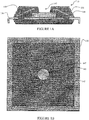
Figures 1A and 1B illustrate a cross-sectional side view and a top view of an open cavityplastic IC package 10 made by the process of the present invention. The open cavityplastic IC package 10 has a die 140 positioned on alead frame 130.Bond wires 135 extend from the die 140 to thelead frame 130. TheIC package 10 is covered with aplastic encapsulant 145, which provides a sensor port or anopen cavity 147 for a sensor on thedie 140 to have access to the ambient conditions in which theIC package 10 may be placed. -
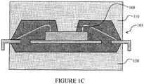
Figure 1C illustrates a cross-sectional side view of theIC package 10 ofFigures 1A and 1B in amold 105. During the manufacturing process, encapsulant in the form of a molding compound is pumped into the mold to cover the interconnects or bond wires. Themold 105 comprises two half-shell molds: a top part of themold 110 and a bottom part of themold 120. Thetop part 110 of the mold has apin 160 that contacts the upper surface of thedie 140 when the mold is assembled on thelead frame 130. Thepin 160 prevents the plastic encapsulant from forming a cover in the area above thedie 140 so that anopen cavity 147 may be formed. -
Figure 2 illustrates a cross-sectional side view of an IC package in a mold of the present invention. Thetop part 110 of themold 105 comprises apin 160. Thepin 160 has apin head 163, which contacts the die 140. Thepin 160 also has aforce element 161 and ananchor element 162. Theanchor element 162 holds thepin 160 in thetop part 110 of themold 105. Theforce element 161 is connected at one end to theanchor element 162 and at the other end to thepin head 163. Theforce element 161 pushes thepin head 163 away from theanchor element 162 toward thedie 140. The force element may take any form known to persons of skill in the art, such as a spring, a piston, an elastic rod, a magnetic rod, etc., wherein it has the capacity to force the position of thepin head 163 toward thedie 140. To provide more uniform contact between thepin head 163 and thedie 140, thepin head 163 may be flexibly or pivotably attached to theforce element 161. A flexible or pivotable attachment may allow thepin head 163 to adjust its contact face to align with thedie 140. This alignment may be particularly beneficial where the die is thicker on one side and relatively thinner on another side, or if the die is not perfectly bonded to the lead frame so as to be the same height at all points.
As IC dies may vary in thickness, the force element works beyond its means to protect the sensor area. Conventional manufacturing devices use a fixed pin and a high-temperature tape to protect the sensor area and form the open cavity. However, because fixed pins may apply different contact pressures to IC dies, depending on the IC die thicknesses, plastic encapsulate or resin may bleed or flow into the open cavity where the sensor is to be positioned or is positioned on the IC die. Further, use of a fixed pin and high-temperature tape may require additional process steps to remove the high-temperature tape. During the removal process, the sensor is further exposed and could be damaged. This conventional process uses a very expensive high-temperature tape to cover the sensor area during encapsulation and then an additional process to remove the high temperature tape from the open cavity either manually or using vacuum. These extra steps add to the unit cost. Also, additional process steps have their own process issues, i.e., they may scratch the sensor or cause resin to bleed into the open cavity over the sensor.
The force or spring-loaded concept according to various embodiments of the invention has been proven not to cause any damage to the sensor area. The technology according to various embodiments utilizes a spring-loaded pin similar to a spring-loaded pogo pin technology only present in equipment handlers for piece part testing (for example, to provide electrical connection of a test device with bond pads on a silicon die).
According to an embodiment, a spring load pogo or pin is used in the transfer molding process to create an opening in plastic packages such as in a Thin Quad Flat No Lead package. A similar concept can be applied to any other plastic package that is used in, for example, a gas or pressure sensor application that requires an opening to expose a sensor area of the device.
Using a spring-loaded pin mold (for example in the top half of a mold), provides an economically sound process without causing any sort of damage to the sensor areas. The spring loaded cavity package furthermore will not cause any damage during the transfer molding process. -
Figure 3 shows a two-part mold according to various embodiments. Thebottom part 120 of the mold provides support for adie 140, which may be placed on alead frame 130. Thetop part 110 includes the spring-moldedpin arrangement 190, wherein apin 160 supporting acover 150 provides for a cover of the sensor area that may be arranged in the center of thedie 140 on thelead frame 130. The spring can be arranged inside aspring housing 170 and extends thecover 150 into or beyond the hollow space 100 when thetop part 110 of the mold is not placed on thebottom part 120 as shown inFigure 3 . Once thetop part 110 of the mold is placed onto thebottom part 120, the spring-loadedpin 160 is pushed back by thedie 140. Anadditional opening 180 can be provided to retract thecover 150. The extension length is designed such that thecover portion 150 of the spring loadedpin arrangement 190 will form an opening in the housing. The spring-loadedpin arrangement 190 further provides for automatic adjustment depending on the thickness of thedie 140. Thus, a singletop mold part 110 can be used with various die thicknesses. Once the mold is closed by putting thetop part 110 of the mold on top of thebottom part 120, plastic can be injected into the hollow space 100 to encompass and seal thedie 140 within the housing and at the same time form the opening in the top portion of the housing. Retracting the top part of the mold leaves the sensing device package completed without damage to the sensor area. -
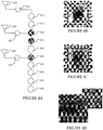
Figure 4A shows the manufacturing process in the form of a flow chart for an IC package of the present invention, wherein the process comprises three sub-processes: die attach, wire bonder, and molding. For the die attach sub-process, a supply ofwafers 410 is brought into the process forinspection 411. The wafers are then mounted 412 and sawed 413. Dies are then attached 422 to the lead frames. A machine, such as an ASM AD898 may be used, wherein the machine may have an automatic wafer handling system with water cassette elevator for up to 8-inch wafers. Such a machine may be capable of handling die sizes from 0.25mm x 0.25mm to 25.4mm x 25.4mm. The machine may also apply a bond force of 30-2000g and provide multi-grey levels PRS.Figure 4B illustrates an IC at the end of the die attach sub-process.
Referring again toFigure 4A , for the wire bonder sub-process, a supply of lead frames 420 is brought into the process forinspection 421. Bond wires are then made to bond 423 the dies to the lead frames. A step called 3rdOptical QA 424 is then performed. This sub-process creates wire-bound integrated circuits. A machine such as an ASM Eagle-60 or equivalent may be used. The wire size may be 15um to 50.8um Au. The maximum length of the wires may be 8mm. The bonding speed may be 60+ ms for 2mm wire. The bond placement accuracy may be ±3.0um. The bonding area may be 54mm x 65mm.Figure 4C illustrates an IC at the end of the wire bonder sub-process.
Referring again toFigure 4A , for the molding sub-process, a supply ofcompound 430 is brought into the process forinspection 431. The wafers are then molded 432 to form the IC packages. The wafers are then marked 433. Asaw singulation step 434 is then performed to separate the IC packages. Avisual inspection 435 is performed, and the ICs are then packed and shipped 436. An ASAHI Cosmo-T machine may be used for the molding sub-process. The mold temperature may be 180°C ±5°C. The transfer pressure may be 35 kgf. The clamp tonnage may be 45 ton. The in-mold cure time may be 90 seconds.Figure 4D illustrates an IC at the end of the molding sub-process.
Materials known to persons of skill in the art may be used to manufacture the ICs. For example, the lead frame may be µPPF 0.2mm thick, wherein the pad size may be 2.90mm x 2.90mm and the exposed pad size may be 2.60mm x 2.60mm. The die-attached epoxy may be Sumitomo CRM1076NS. Gold wire may be used having a diameter of MKE 0.8 mils. A mold compound may be Sumitomo G770HCD, wherein the pellet size may be 14 x 6.0g. -
Figures 5A - 5C show top, side, and bottom views of anIC package 10 of an environmental sensor using a TQFN package. The depth of theopen cavity 147 may be about 0.35mm ±0.05, and the diameter of theopen cavity 147 may be about 1mm, for a package that is about 4mm square. Thelead frame 130 is visible from the side and bottom, as shown inFigures 5B and 5C , respectively. -
Figures 6A and 6B show a lead frame and a top mold cavity design for an array of sensor devices, whereinFigure 6A is a top view of theentire array 605, andFigure 6B is a cross-sectional side view of a portion of thearray 605. The exemplary top mold cavity design has fourpanels 610, wherein eachpanel 610 is a 10 x 12 a for anarray 610 having a total of 480 ICs. Eachpanel 610 has alead frame 130 with an array of dies 140, wherein apin 160 is used relative to each die 140 to form an open cavity for a sensor on the die. According to one embodiment, thearray 605 may be a TQFN top mold cavity design for TQFN 4x4 pressure sensor. -
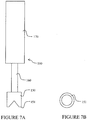
Figures 7A and 7B show an exemplary embodiment of the spring-loaded pin arrangement according to the invention.Figure 7A is a side view of a spring-moldedpin arrangement 190. The spring-moldedpin arrangement 190 comprises aspring housing 170, apin 160, and acover 150.Figure 7B is an end view of thecover 150. Thecover 150 has anannular contact face 151 that allows thecover 150 to make more uniform contact with the die 140 (seeFigure 3 ) to prevent flashing of the plastic encapsulant into the open cavity 147 (seeFigure 1A ). The outside diameter of thecover 150 is 1.2mm, and the inside diameter of the conical recess in thecover 150 is 1.0mm, so that theannular contact face 151 may be about .1mm wide. The spring-moldedpin arrangement 190 may be constructed of material sufficient to endure exposure to plastic encapsulant heated to at least 300°C. The force of the spring inside thespring housing 170 is 80-120g. - In alternative embodiments of the invention, a plurality of open cavities may be formed on a single IC. To form a plurality of open cavities, a plurality of
covers 150 or pin heads 163 may be applied to a single IC during a molding sub-process. Where a plurality of pins are independently forced against the die, the independent application of force may ensure that the plastic encapsulant is unable to enter any of the open cavities because the plurality of pins are each able to make a firm contact with the die. Alternatively, asingle cover 150 orpin head 163 may be applied to a single IC during a molding sub-process, but thesingle cover 150 orpin head 163 comprises a plurality of contact faces 151. In the embodiment illustrated inFigure 7B , thecontact face 151 is annular, but in alternatively embodiments, the contact face may be any shape or configuration and may comprise a plurality of contact faces. A plurality ofopen cavities 147 may be useful where a plurality of sensors are attached to a single IC.
Claims (10)
- A mold for forming a package for an integrated circuit sensor device, comprising
a bottom part (120) for supporting an integrated circuit die (140);
a top part (110) that is operable to be placed on top of said bottom part (120) to form a cavity into which a plastic material can be injected to form the package, wherein the top part (110) of the mold comprises a spring housing (170) of a spring-loaded pin arrangement (190) further comprising a cylindrical cover (150) made from high temperature plastic material and having a recess configured to cover a sensor area on the integrated circuit die and wherein the top part (110) further provides for an injection opening to allow injection of the plastic material, a pin (160) extending from the cylindrical cover (150) and guided within the spring housing (170) wherein the pin (160) can be vertically moved against a spring force,
wherein the top part (110) further comprises a recess (180) extending from the opening towards said cavity and configured to receive the cylindrical cover (150) when the top part (110 is placed on said bottom part (120),
wherein the pin (160) can extend 4 to 5 mm from the spring housing (170) and wherein the spring provides for a spring force of 80-120g. - The mold according to claim 1, wherein the cylindrical cover (150) comprises an annular contact face (151) and a conical recess.
- The mold according to claim 2, wherein an outside diameter of the cylindrical cover is 1.2 mm wide.
- The mold according to claim 3, wherein the inside diameter of the cylindrical cover (150) is 1.0 mm.
- The mold according to one of the preceding claims, comprising a plurality of spring-loaded pin arrangements, each comprising a cylindrical cover (150) that covers a sensor area on the integrated circuit die (140).
- A process of manufacturing an open cavity integrated circuit package using a mold according to one of the preceding claims, the method comprising:placing a wire-bound integrated circuit in the mold (110, 120);forcing the cylindrical cover (150) to contact the die (140) of the wire-bound integrated circuit by applying a force between the pin (160) and the mold (110);injecting plastic into the mold (110, 120);allowing the plastic to set around the integrated circuit to form a package having an open cavity defined by the cylindrical cover (150); andremoving the open cavity integrated circuit package from the mold (110, 120).
- The process of manufacturing an open cavity integrated circuit package as claimed in claim 6, wherein the forcing a pin to contact a die comprises applying a spring force.
- The process of manufacturing an open cavity integrated circuit package according to one of the preceding claims 6-7, wherein the forcing a pin to contact a die comprises forcing a plurality of pins to contact a die, and wherein the allowing the plastic to set comprises allowing the plastic to set around the plurality of pins to form a plurality of open cavities defined by the plurality of pins.
- The process of manufacturing an open cavity integrated circuit package according to one of the preceding claims 6-8, further comprising pivoting the pin (160) relative to the mold (110, 120) for uniform contact of a cylindrical cover contact face (151) with the die (140).
- The process of manufacturing an open cavity integrated circuit package according to one of the preceding claims 6-9, wherein the placing a wire-bound integrated circuit in a mold (110, 120) comprises placing an array of wire-bound integrated circuits in a mold; wherein forcing a cylindrical cover (150) to contact a die (140) comprises forcing a corresponding array of pins to contact the dies of the array of wire-bound integrated circuits; and wherein allowing the plastic to set comprises allowing the plastic to set around the array of integrated circuit to form an array of packages having open cavities defined by the array of pins.
Applications Claiming Priority (3)
| Application Number | Priority Date | Filing Date | Title |
|---|---|---|---|
| US201361755889P | 2013-01-23 | 2013-01-23 | |
| US14/157,382 US9269597B2 (en) | 2013-01-23 | 2014-01-16 | Open cavity plastic package |
| PCT/US2014/012512 WO2014116677A1 (en) | 2013-01-23 | 2014-01-22 | Open cavity plastic package |
Publications (2)
| Publication Number | Publication Date |
|---|---|
| EP2948979A1 EP2948979A1 (en) | 2015-12-02 |
| EP2948979B1 true EP2948979B1 (en) | 2020-08-05 |
Family
ID=51208008
Family Applications (1)
| Application Number | Title | Priority Date | Filing Date |
|---|---|---|---|
| EP14702428.5A Active EP2948979B1 (en) | 2013-01-23 | 2014-01-22 | Open cavity plastic package |
Country Status (6)
| Country | Link |
|---|---|
| US (2) | US9269597B2 (en) |
| EP (1) | EP2948979B1 (en) |
| KR (1) | KR20150111972A (en) |
| CN (1) | CN104969336B (en) |
| TW (1) | TWI604577B (en) |
| WO (1) | WO2014116677A1 (en) |
Families Citing this family (18)
| Publication number | Priority date | Publication date | Assignee | Title |
|---|---|---|---|---|
| JP5583487B2 (en) * | 2010-06-14 | 2014-09-03 | 矢崎総業株式会社 | Fuse unit, mold structure, and molding method using mold structure |
| US9269597B2 (en) | 2013-01-23 | 2016-02-23 | Microchip Technology Incorporated | Open cavity plastic package |
| ES2768272T3 (en) * | 2014-03-05 | 2020-06-22 | Yazaki Europe Ltd | Molding tool |
| DE112014007140B4 (en) * | 2014-11-07 | 2024-05-02 | Mitsubishi Electric Corporation | Power semiconductor device and method for producing the same |
| US9355870B1 (en) | 2015-01-15 | 2016-05-31 | Silicon Laboratories Inc. | Integrated circuit with sensor area and resin dam |
| US9431311B1 (en) | 2015-02-19 | 2016-08-30 | Semiconductor Components Industries, Llc | Semiconductor package with elastic coupler and related methods |
| JP6079925B1 (en) * | 2016-03-30 | 2017-02-15 | 第一精工株式会社 | Resin sealing device and abnormality detection method of resin sealing device |
| JP6319399B2 (en) * | 2016-10-28 | 2018-05-09 | 株式会社デンソー | Insert mold |
| US10199356B2 (en) | 2017-02-24 | 2019-02-05 | Micron Technology, Inc. | Semiconductor device assembles with electrically functional heat transfer structures |
| US10090282B1 (en) * | 2017-06-13 | 2018-10-02 | Micron Technology, Inc. | Semiconductor device assemblies with lids including circuit elements |
| DE102017131110B4 (en) * | 2017-12-22 | 2025-01-02 | OSRAM Opto Semiconductors Gesellschaft mit beschränkter Haftung | METHOD AND MOULD FOR EMBEDDING OPTOELECTRONIC COMPONENTS IN A LAYER |
| JP7331571B2 (en) * | 2019-09-17 | 2023-08-23 | I-Pex株式会社 | Resin encapsulation mold and resin encapsulation method |
| DE102020201666A1 (en) * | 2020-02-11 | 2021-08-12 | Robert Bosch Gesellschaft mit beschränkter Haftung | Mold device with automatically clogging shot channel |
| WO2022021094A1 (en) * | 2020-07-28 | 2022-02-03 | 华为技术有限公司 | Power module, and preparation mold and apparatus |
| US12309954B1 (en) | 2020-09-10 | 2025-05-20 | Verily Life Sciences Llc | Protective structures with integrated electrical interconnects for active implantable medical devices |
| US20220221353A1 (en) * | 2021-01-12 | 2022-07-14 | Texas Instruments Incorporated | Semiconductor force sensors |
| CN113451238B (en) * | 2021-07-16 | 2022-06-21 | 贵州中芯微电子科技有限公司 | A hollow integrated circuit package |
| CN118486612B (en) * | 2024-06-03 | 2025-10-14 | 安徽丰芯半导体有限公司 | Die assembly for chip package |
Citations (3)
| Publication number | Priority date | Publication date | Assignee | Title |
|---|---|---|---|---|
| JPS5963735A (en) * | 1982-10-05 | 1984-04-11 | Rohm Co Ltd | Manufacture of semiconductor device |
| JPH09304211A (en) * | 1996-05-15 | 1997-11-28 | Omron Corp | Capacitive pressure sensor packaging structure and packaging method |
| WO2003028086A1 (en) * | 2001-09-26 | 2003-04-03 | European Semiconductor Assembly (Eurasem) B.V. | Method for encapsulating a chip and/or other article |
Family Cites Families (15)
| Publication number | Priority date | Publication date | Assignee | Title |
|---|---|---|---|---|
| US4452420A (en) * | 1982-09-30 | 1984-06-05 | Lynn Lundquist | Compensating core pin for plastic injection molds |
| JP2705361B2 (en) | 1991-05-30 | 1998-01-28 | 三菱電機株式会社 | Mold for manufacturing hollow type resin-sealed semiconductor pressure sensor |
| SE514116C2 (en) * | 1994-10-19 | 2001-01-08 | Ericsson Telefon Ab L M | Process for producing a nested optocomponent, mold for encapsulating an optocomponent and molding device |
| JP4024335B2 (en) | 1996-01-26 | 2007-12-19 | ハリス コーポレイション | Integrated circuit device having an opening exposing die of integrated circuit and manufacturing method thereof |
| US5997798A (en) * | 1997-06-27 | 1999-12-07 | International Business Machines Corporation | Biasing mold for integrated circuit chip assembly encapsulation |
| EP1220309A1 (en) | 2000-12-28 | 2002-07-03 | STMicroelectronics S.r.l. | Manufacturing method of an electronic device package |
| US7304362B2 (en) | 2002-05-20 | 2007-12-04 | Stmicroelectronics, Inc. | Molded integrated circuit package with exposed active area |
| US7109574B2 (en) | 2002-07-26 | 2006-09-19 | Stmicroelectronics, Inc. | Integrated circuit package with exposed die surfaces and auxiliary attachment |
| JP4519424B2 (en) * | 2003-06-26 | 2010-08-04 | ルネサスエレクトロニクス株式会社 | Resin mold type semiconductor device |
| DE102005010311A1 (en) * | 2005-03-03 | 2006-09-14 | Atmel Germany Gmbh | Method and mold for producing an optical semiconductor module |
| JP2008066696A (en) * | 2006-08-10 | 2008-03-21 | Denso Corp | Semiconductor manufacturing apparatus and semiconductor manufacturing method |
| DE102011004381A1 (en) | 2011-02-18 | 2012-08-23 | Robert Bosch Gmbh | Mold module with sensor element |
| EP2573804A1 (en) | 2011-09-21 | 2013-03-27 | Nxp B.V. | Integrated circuit with sensor and manufacturing method thereof |
| US8501517B1 (en) * | 2012-04-09 | 2013-08-06 | Freescale Semiconductor, Inc. | Method of assembling pressure sensor device |
| US9269597B2 (en) | 2013-01-23 | 2016-02-23 | Microchip Technology Incorporated | Open cavity plastic package |
-
2014
- 2014-01-16 US US14/157,382 patent/US9269597B2/en active Active
- 2014-01-22 CN CN201480005724.3A patent/CN104969336B/en active Active
- 2014-01-22 KR KR1020157022855A patent/KR20150111972A/en not_active Ceased
- 2014-01-22 EP EP14702428.5A patent/EP2948979B1/en active Active
- 2014-01-22 WO PCT/US2014/012512 patent/WO2014116677A1/en not_active Ceased
- 2014-01-23 TW TW103102595A patent/TWI604577B/en active
-
2016
- 2016-02-22 US US15/050,438 patent/US9630352B2/en active Active
Patent Citations (3)
| Publication number | Priority date | Publication date | Assignee | Title |
|---|---|---|---|---|
| JPS5963735A (en) * | 1982-10-05 | 1984-04-11 | Rohm Co Ltd | Manufacture of semiconductor device |
| JPH09304211A (en) * | 1996-05-15 | 1997-11-28 | Omron Corp | Capacitive pressure sensor packaging structure and packaging method |
| WO2003028086A1 (en) * | 2001-09-26 | 2003-04-03 | European Semiconductor Assembly (Eurasem) B.V. | Method for encapsulating a chip and/or other article |
Also Published As
| Publication number | Publication date |
|---|---|
| EP2948979A1 (en) | 2015-12-02 |
| CN104969336A (en) | 2015-10-07 |
| US9269597B2 (en) | 2016-02-23 |
| KR20150111972A (en) | 2015-10-06 |
| CN104969336B (en) | 2019-02-01 |
| TWI604577B (en) | 2017-11-01 |
| US20160167273A1 (en) | 2016-06-16 |
| TW201438163A (en) | 2014-10-01 |
| WO2014116677A1 (en) | 2014-07-31 |
| US20140206122A1 (en) | 2014-07-24 |
| US9630352B2 (en) | 2017-04-25 |
Similar Documents
| Publication | Publication Date | Title |
|---|---|---|
| US9630352B2 (en) | Open cavity plastic package | |
| EP1465244B1 (en) | Integrated circuit package with exposed die surfaces and auxiliary attachment | |
| KR970006531B1 (en) | Electronic device package and manufacturing method | |
| KR101031394B1 (en) | Light sensor package | |
| EP3026696B1 (en) | Package for semiconductor devices sensitive to mechanical and thermo-mechanical stresses, such as mems pressure sensors | |
| US7582954B1 (en) | Optical leadless leadframe package | |
| US20140374848A1 (en) | Semiconductor sensor device with metal lid | |
| US20050279166A1 (en) | Semiconductor acceleration sensor device and method for manufacturing the same | |
| US20090314095A1 (en) | Pressure sensing device package and manufacturing method thereof | |
| US5378656A (en) | Leadframe, semiconductor integrated circuit device using the same, and method of and process for fabricating the same | |
| US20050184404A1 (en) | Photosensitive semiconductor package with support member and method for fabricating the same | |
| US20130119538A1 (en) | Wafer level chip size package | |
| JP6598642B2 (en) | Resin sealing device and resin sealing method | |
| US6291263B1 (en) | Method of fabricating an integrated circuit package having a core-hollowed encapsulation body | |
| CN100495689C (en) | Method of packaging an optical sensor and image sensor device | |
| US20050082490A1 (en) | Optical semiconductor housing with transparent chip and method for making same | |
| US20150035130A1 (en) | Integrated Circuit with Stress Isolation | |
| US8237293B2 (en) | Semiconductor package with protective tape | |
| KR20160081289A (en) | Boat for semiconductor package fabrication and method for fabricating the semiconductor package | |
| JP2000176967A (en) | Resin sealing device | |
| US9368424B2 (en) | Method of fabricating a semiconductor device used in a stacked-type semiconductor device | |
| KR20090066517A (en) | Wafer Level Semiconductor Package and Manufacturing Method Thereof | |
| TWI837600B (en) | Package structure and manufacturing apparatus thereof | |
| JP2011014606A (en) | Method of manufacturing semiconductor apparatus | |
| CN115881684A (en) | Strip for chip packaging, packaging module and smart card |
Legal Events
| Date | Code | Title | Description |
|---|---|---|---|
| PUAI | Public reference made under article 153(3) epc to a published international application that has entered the european phase |
Free format text: ORIGINAL CODE: 0009012 |
|
| 17P | Request for examination filed |
Effective date: 20150820 |
|
| AK | Designated contracting states |
Kind code of ref document: A1 Designated state(s): AL AT BE BG CH CY CZ DE DK EE ES FI FR GB GR HR HU IE IS IT LI LT LU LV MC MK MT NL NO PL PT RO RS SE SI SK SM TR |
|
| AX | Request for extension of the european patent |
Extension state: BA ME |
|
| DAX | Request for extension of the european patent (deleted) | ||
| STAA | Information on the status of an ep patent application or granted ep patent |
Free format text: STATUS: EXAMINATION IS IN PROGRESS |
|
| 17Q | First examination report despatched |
Effective date: 20161129 |
|
| GRAP | Despatch of communication of intention to grant a patent |
Free format text: ORIGINAL CODE: EPIDOSNIGR1 |
|
| STAA | Information on the status of an ep patent application or granted ep patent |
Free format text: STATUS: GRANT OF PATENT IS INTENDED |
|
| INTG | Intention to grant announced |
Effective date: 20200224 |
|
| GRAS | Grant fee paid |
Free format text: ORIGINAL CODE: EPIDOSNIGR3 |
|
| GRAA | (expected) grant |
Free format text: ORIGINAL CODE: 0009210 |
|
| STAA | Information on the status of an ep patent application or granted ep patent |
Free format text: STATUS: THE PATENT HAS BEEN GRANTED |
|
| AK | Designated contracting states |
Kind code of ref document: B1 Designated state(s): AL AT BE BG CH CY CZ DE DK EE ES FI FR GB GR HR HU IE IS IT LI LT LU LV MC MK MT NL NO PL PT RO RS SE SI SK SM TR |
|
| REG | Reference to a national code |
Ref country code: GB Ref legal event code: FG4D |
|
| REG | Reference to a national code |
Ref country code: CH Ref legal event code: EP |
|
| REG | Reference to a national code |
Ref country code: AT Ref legal event code: REF Ref document number: 1299909 Country of ref document: AT Kind code of ref document: T Effective date: 20200815 |
|
| REG | Reference to a national code |
Ref country code: DE Ref legal event code: R096 Ref document number: 602014068525 Country of ref document: DE |
|
| REG | Reference to a national code |
Ref country code: IE Ref legal event code: FG4D |
|
| REG | Reference to a national code |
Ref country code: LT Ref legal event code: MG4D |
|
| REG | Reference to a national code |
Ref country code: NL Ref legal event code: MP Effective date: 20200805 |
|
| REG | Reference to a national code |
Ref country code: AT Ref legal event code: MK05 Ref document number: 1299909 Country of ref document: AT Kind code of ref document: T Effective date: 20200805 |
|
| PG25 | Lapsed in a contracting state [announced via postgrant information from national office to epo] |
Ref country code: LT Free format text: LAPSE BECAUSE OF FAILURE TO SUBMIT A TRANSLATION OF THE DESCRIPTION OR TO PAY THE FEE WITHIN THE PRESCRIBED TIME-LIMIT Effective date: 20200805 Ref country code: ES Free format text: LAPSE BECAUSE OF FAILURE TO SUBMIT A TRANSLATION OF THE DESCRIPTION OR TO PAY THE FEE WITHIN THE PRESCRIBED TIME-LIMIT Effective date: 20200805 Ref country code: BG Free format text: LAPSE BECAUSE OF FAILURE TO SUBMIT A TRANSLATION OF THE DESCRIPTION OR TO PAY THE FEE WITHIN THE PRESCRIBED TIME-LIMIT Effective date: 20201105 Ref country code: HR Free format text: LAPSE BECAUSE OF FAILURE TO SUBMIT A TRANSLATION OF THE DESCRIPTION OR TO PAY THE FEE WITHIN THE PRESCRIBED TIME-LIMIT Effective date: 20200805 Ref country code: NO Free format text: LAPSE BECAUSE OF FAILURE TO SUBMIT A TRANSLATION OF THE DESCRIPTION OR TO PAY THE FEE WITHIN THE PRESCRIBED TIME-LIMIT Effective date: 20201105 Ref country code: PT Free format text: LAPSE BECAUSE OF FAILURE TO SUBMIT A TRANSLATION OF THE DESCRIPTION OR TO PAY THE FEE WITHIN THE PRESCRIBED TIME-LIMIT Effective date: 20201207 Ref country code: FI Free format text: LAPSE BECAUSE OF FAILURE TO SUBMIT A TRANSLATION OF THE DESCRIPTION OR TO PAY THE FEE WITHIN THE PRESCRIBED TIME-LIMIT Effective date: 20200805 Ref country code: GR Free format text: LAPSE BECAUSE OF FAILURE TO SUBMIT A TRANSLATION OF THE DESCRIPTION OR TO PAY THE FEE WITHIN THE PRESCRIBED TIME-LIMIT Effective date: 20201106 Ref country code: SE Free format text: LAPSE BECAUSE OF FAILURE TO SUBMIT A TRANSLATION OF THE DESCRIPTION OR TO PAY THE FEE WITHIN THE PRESCRIBED TIME-LIMIT Effective date: 20200805 Ref country code: AT Free format text: LAPSE BECAUSE OF FAILURE TO SUBMIT A TRANSLATION OF THE DESCRIPTION OR TO PAY THE FEE WITHIN THE PRESCRIBED TIME-LIMIT Effective date: 20200805 |
|
| PG25 | Lapsed in a contracting state [announced via postgrant information from national office to epo] |
Ref country code: IS Free format text: LAPSE BECAUSE OF FAILURE TO SUBMIT A TRANSLATION OF THE DESCRIPTION OR TO PAY THE FEE WITHIN THE PRESCRIBED TIME-LIMIT Effective date: 20201205 Ref country code: RS Free format text: LAPSE BECAUSE OF FAILURE TO SUBMIT A TRANSLATION OF THE DESCRIPTION OR TO PAY THE FEE WITHIN THE PRESCRIBED TIME-LIMIT Effective date: 20200805 Ref country code: PL Free format text: LAPSE BECAUSE OF FAILURE TO SUBMIT A TRANSLATION OF THE DESCRIPTION OR TO PAY THE FEE WITHIN THE PRESCRIBED TIME-LIMIT Effective date: 20200805 Ref country code: LV Free format text: LAPSE BECAUSE OF FAILURE TO SUBMIT A TRANSLATION OF THE DESCRIPTION OR TO PAY THE FEE WITHIN THE PRESCRIBED TIME-LIMIT Effective date: 20200805 Ref country code: NL Free format text: LAPSE BECAUSE OF FAILURE TO SUBMIT A TRANSLATION OF THE DESCRIPTION OR TO PAY THE FEE WITHIN THE PRESCRIBED TIME-LIMIT Effective date: 20200805 |
|
| PG25 | Lapsed in a contracting state [announced via postgrant information from national office to epo] |
Ref country code: RO Free format text: LAPSE BECAUSE OF FAILURE TO SUBMIT A TRANSLATION OF THE DESCRIPTION OR TO PAY THE FEE WITHIN THE PRESCRIBED TIME-LIMIT Effective date: 20200805 Ref country code: SM Free format text: LAPSE BECAUSE OF FAILURE TO SUBMIT A TRANSLATION OF THE DESCRIPTION OR TO PAY THE FEE WITHIN THE PRESCRIBED TIME-LIMIT Effective date: 20200805 Ref country code: CZ Free format text: LAPSE BECAUSE OF FAILURE TO SUBMIT A TRANSLATION OF THE DESCRIPTION OR TO PAY THE FEE WITHIN THE PRESCRIBED TIME-LIMIT Effective date: 20200805 Ref country code: DK Free format text: LAPSE BECAUSE OF FAILURE TO SUBMIT A TRANSLATION OF THE DESCRIPTION OR TO PAY THE FEE WITHIN THE PRESCRIBED TIME-LIMIT Effective date: 20200805 Ref country code: EE Free format text: LAPSE BECAUSE OF FAILURE TO SUBMIT A TRANSLATION OF THE DESCRIPTION OR TO PAY THE FEE WITHIN THE PRESCRIBED TIME-LIMIT Effective date: 20200805 |
|
| REG | Reference to a national code |
Ref country code: DE Ref legal event code: R097 Ref document number: 602014068525 Country of ref document: DE |
|
| PG25 | Lapsed in a contracting state [announced via postgrant information from national office to epo] |
Ref country code: AL Free format text: LAPSE BECAUSE OF FAILURE TO SUBMIT A TRANSLATION OF THE DESCRIPTION OR TO PAY THE FEE WITHIN THE PRESCRIBED TIME-LIMIT Effective date: 20200805 |
|
| PLBE | No opposition filed within time limit |
Free format text: ORIGINAL CODE: 0009261 |
|
| STAA | Information on the status of an ep patent application or granted ep patent |
Free format text: STATUS: NO OPPOSITION FILED WITHIN TIME LIMIT |
|
| PG25 | Lapsed in a contracting state [announced via postgrant information from national office to epo] |
Ref country code: SK Free format text: LAPSE BECAUSE OF FAILURE TO SUBMIT A TRANSLATION OF THE DESCRIPTION OR TO PAY THE FEE WITHIN THE PRESCRIBED TIME-LIMIT Effective date: 20200805 |
|
| 26N | No opposition filed |
Effective date: 20210507 |
|
| PG25 | Lapsed in a contracting state [announced via postgrant information from national office to epo] |
Ref country code: IT Free format text: LAPSE BECAUSE OF FAILURE TO SUBMIT A TRANSLATION OF THE DESCRIPTION OR TO PAY THE FEE WITHIN THE PRESCRIBED TIME-LIMIT Effective date: 20200805 |
|
| PG25 | Lapsed in a contracting state [announced via postgrant information from national office to epo] |
Ref country code: SI Free format text: LAPSE BECAUSE OF FAILURE TO SUBMIT A TRANSLATION OF THE DESCRIPTION OR TO PAY THE FEE WITHIN THE PRESCRIBED TIME-LIMIT Effective date: 20200805 Ref country code: MC Free format text: LAPSE BECAUSE OF FAILURE TO SUBMIT A TRANSLATION OF THE DESCRIPTION OR TO PAY THE FEE WITHIN THE PRESCRIBED TIME-LIMIT Effective date: 20200805 |
|
| REG | Reference to a national code |
Ref country code: CH Ref legal event code: PL |
|
| GBPC | Gb: european patent ceased through non-payment of renewal fee |
Effective date: 20210122 |
|
| PG25 | Lapsed in a contracting state [announced via postgrant information from national office to epo] |
Ref country code: LU Free format text: LAPSE BECAUSE OF NON-PAYMENT OF DUE FEES Effective date: 20210122 |
|
| REG | Reference to a national code |
Ref country code: BE Ref legal event code: MM Effective date: 20210131 |
|
| PG25 | Lapsed in a contracting state [announced via postgrant information from national office to epo] |
Ref country code: FR Free format text: LAPSE BECAUSE OF NON-PAYMENT OF DUE FEES Effective date: 20210131 |
|
| PG25 | Lapsed in a contracting state [announced via postgrant information from national office to epo] |
Ref country code: LI Free format text: LAPSE BECAUSE OF NON-PAYMENT OF DUE FEES Effective date: 20210131 Ref country code: GB Free format text: LAPSE BECAUSE OF NON-PAYMENT OF DUE FEES Effective date: 20210122 Ref country code: CH Free format text: LAPSE BECAUSE OF NON-PAYMENT OF DUE FEES Effective date: 20210131 |
|
| PG25 | Lapsed in a contracting state [announced via postgrant information from national office to epo] |
Ref country code: IE Free format text: LAPSE BECAUSE OF NON-PAYMENT OF DUE FEES Effective date: 20210122 |
|
| PG25 | Lapsed in a contracting state [announced via postgrant information from national office to epo] |
Ref country code: IS Free format text: LAPSE BECAUSE OF FAILURE TO SUBMIT A TRANSLATION OF THE DESCRIPTION OR TO PAY THE FEE WITHIN THE PRESCRIBED TIME-LIMIT Effective date: 20201205 |
|
| PG25 | Lapsed in a contracting state [announced via postgrant information from national office to epo] |
Ref country code: BE Free format text: LAPSE BECAUSE OF NON-PAYMENT OF DUE FEES Effective date: 20210131 |
|
| PG25 | Lapsed in a contracting state [announced via postgrant information from national office to epo] |
Ref country code: HU Free format text: LAPSE BECAUSE OF FAILURE TO SUBMIT A TRANSLATION OF THE DESCRIPTION OR TO PAY THE FEE WITHIN THE PRESCRIBED TIME-LIMIT; INVALID AB INITIO Effective date: 20140122 |
|
| PG25 | Lapsed in a contracting state [announced via postgrant information from national office to epo] |
Ref country code: CY Free format text: LAPSE BECAUSE OF FAILURE TO SUBMIT A TRANSLATION OF THE DESCRIPTION OR TO PAY THE FEE WITHIN THE PRESCRIBED TIME-LIMIT Effective date: 20200805 |
|
| P01 | Opt-out of the competence of the unified patent court (upc) registered |
Effective date: 20230528 |
|
| PG25 | Lapsed in a contracting state [announced via postgrant information from national office to epo] |
Ref country code: MK Free format text: LAPSE BECAUSE OF FAILURE TO SUBMIT A TRANSLATION OF THE DESCRIPTION OR TO PAY THE FEE WITHIN THE PRESCRIBED TIME-LIMIT Effective date: 20200805 |
|
| PG25 | Lapsed in a contracting state [announced via postgrant information from national office to epo] |
Ref country code: MT Free format text: LAPSE BECAUSE OF FAILURE TO SUBMIT A TRANSLATION OF THE DESCRIPTION OR TO PAY THE FEE WITHIN THE PRESCRIBED TIME-LIMIT Effective date: 20200805 |
|
| REG | Reference to a national code |
Ref country code: DE Ref legal event code: R079 Ref document number: 602014068525 Country of ref document: DE Free format text: PREVIOUS MAIN CLASS: H01L0021560000 Ipc: H10W0074010000 |
|
| PG25 | Lapsed in a contracting state [announced via postgrant information from national office to epo] |
Ref country code: TR Free format text: LAPSE BECAUSE OF FAILURE TO SUBMIT A TRANSLATION OF THE DESCRIPTION OR TO PAY THE FEE WITHIN THE PRESCRIBED TIME-LIMIT Effective date: 20200805 |
|
| PGFP | Annual fee paid to national office [announced via postgrant information from national office to epo] |
Ref country code: DE Payment date: 20251217 Year of fee payment: 13 |