EP2947680A1 - Semiconductor device - Google Patents
Semiconductor device Download PDFInfo
- Publication number
- EP2947680A1 EP2947680A1 EP13871657.6A EP13871657A EP2947680A1 EP 2947680 A1 EP2947680 A1 EP 2947680A1 EP 13871657 A EP13871657 A EP 13871657A EP 2947680 A1 EP2947680 A1 EP 2947680A1
- Authority
- EP
- European Patent Office
- Prior art keywords
- wiring
- input voltage
- ground voltage
- nmos transistor
- semiconductor device
- Prior art date
- Legal status (The legal status is an assumption and is not a legal conclusion. Google has not performed a legal analysis and makes no representation as to the accuracy of the status listed.)
- Withdrawn
Links
Images

Classifications
-
- H—ELECTRICITY
- H10—SEMICONDUCTOR DEVICES; ELECTRIC SOLID-STATE DEVICES NOT OTHERWISE PROVIDED FOR
- H10D—INORGANIC ELECTRIC SEMICONDUCTOR DEVICES
- H10D89/00—Aspects of integrated devices not covered by groups H10D84/00 - H10D88/00
- H10D89/60—Integrated devices comprising arrangements for electrical or thermal protection, e.g. protection circuits against electrostatic discharge [ESD]
- H10D89/601—Integrated devices comprising arrangements for electrical or thermal protection, e.g. protection circuits against electrostatic discharge [ESD] for devices having insulated gate electrodes, e.g. for IGFETs or IGBTs
- H10D89/811—Integrated devices comprising arrangements for electrical or thermal protection, e.g. protection circuits against electrostatic discharge [ESD] for devices having insulated gate electrodes, e.g. for IGFETs or IGBTs using FETs as protective elements
-
- H—ELECTRICITY
- H10—SEMICONDUCTOR DEVICES; ELECTRIC SOLID-STATE DEVICES NOT OTHERWISE PROVIDED FOR
- H10D—INORGANIC ELECTRIC SEMICONDUCTOR DEVICES
- H10D64/00—Electrodes of devices having potential barriers
- H10D64/20—Electrodes characterised by their shapes, relative sizes or dispositions
- H10D64/23—Electrodes carrying the current to be rectified, amplified, oscillated or switched, e.g. sources, drains, anodes or cathodes
- H10D64/251—Source or drain electrodes for field-effect devices
- H10D64/257—Source or drain electrodes for field-effect devices for lateral devices wherein the source or drain electrodes are characterised by top-view geometrical layouts, e.g. interdigitated, semi-circular, annular or L-shaped electrodes
-
- H—ELECTRICITY
- H10—SEMICONDUCTOR DEVICES; ELECTRIC SOLID-STATE DEVICES NOT OTHERWISE PROVIDED FOR
- H10D—INORGANIC ELECTRIC SEMICONDUCTOR DEVICES
- H10D64/00—Electrodes of devices having potential barriers
- H10D64/20—Electrodes characterised by their shapes, relative sizes or dispositions
- H10D64/27—Electrodes not carrying the current to be rectified, amplified, oscillated or switched, e.g. gates
- H10D64/311—Gate electrodes for field-effect devices
- H10D64/411—Gate electrodes for field-effect devices for FETs
- H10D64/511—Gate electrodes for field-effect devices for FETs for IGFETs
- H10D64/517—Gate electrodes for field-effect devices for FETs for IGFETs characterised by the conducting layers
- H10D64/519—Gate electrodes for field-effect devices for FETs for IGFETs characterised by the conducting layers characterised by their top-view geometrical layouts
-
- H—ELECTRICITY
- H10—SEMICONDUCTOR DEVICES; ELECTRIC SOLID-STATE DEVICES NOT OTHERWISE PROVIDED FOR
- H10D—INORGANIC ELECTRIC SEMICONDUCTOR DEVICES
- H10D89/00—Aspects of integrated devices not covered by groups H10D84/00 - H10D88/00
- H10D89/10—Integrated device layouts
-
- H—ELECTRICITY
- H10—SEMICONDUCTOR DEVICES; ELECTRIC SOLID-STATE DEVICES NOT OTHERWISE PROVIDED FOR
- H10D—INORGANIC ELECTRIC SEMICONDUCTOR DEVICES
- H10D89/00—Aspects of integrated devices not covered by groups H10D84/00 - H10D88/00
- H10D89/60—Integrated devices comprising arrangements for electrical or thermal protection, e.g. protection circuits against electrostatic discharge [ESD]
- H10D89/601—Integrated devices comprising arrangements for electrical or thermal protection, e.g. protection circuits against electrostatic discharge [ESD] for devices having insulated gate electrodes, e.g. for IGFETs or IGBTs
- H10D89/811—Integrated devices comprising arrangements for electrical or thermal protection, e.g. protection circuits against electrostatic discharge [ESD] for devices having insulated gate electrodes, e.g. for IGFETs or IGBTs using FETs as protective elements
- H10D89/813—Integrated devices comprising arrangements for electrical or thermal protection, e.g. protection circuits against electrostatic discharge [ESD] for devices having insulated gate electrodes, e.g. for IGFETs or IGBTs using FETs as protective elements specially adapted to provide an electrical current path other than the field-effect induced current path
- H10D89/815—Integrated devices comprising arrangements for electrical or thermal protection, e.g. protection circuits against electrostatic discharge [ESD] for devices having insulated gate electrodes, e.g. for IGFETs or IGBTs using FETs as protective elements specially adapted to provide an electrical current path other than the field-effect induced current path involving a parasitic bipolar transistor triggered by the local electrical biasing of the layer acting as base region of said parasitic bipolar transistor
-
- H—ELECTRICITY
- H10—SEMICONDUCTOR DEVICES; ELECTRIC SOLID-STATE DEVICES NOT OTHERWISE PROVIDED FOR
- H10W—GENERIC PACKAGES, INTERCONNECTIONS, CONNECTORS OR OTHER CONSTRUCTIONAL DETAILS OF DEVICES COVERED BY CLASS H10
- H10W20/00—Interconnections in chips, wafers or substrates
- H10W20/20—Interconnections within wafers or substrates, e.g. through-silicon vias [TSV]
-
- H—ELECTRICITY
- H10—SEMICONDUCTOR DEVICES; ELECTRIC SOLID-STATE DEVICES NOT OTHERWISE PROVIDED FOR
- H10D—INORGANIC ELECTRIC SEMICONDUCTOR DEVICES
- H10D30/00—Field-effect transistors [FET]
- H10D30/60—Insulated-gate field-effect transistors [IGFET]
Definitions
- the present invention relates to a semiconductor device having an NMOS transistor for an electrostatic discharge (ESD) protection circuit.
- ESD electrostatic discharge
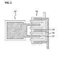
- FIG. 2 is a plan view of the related-art semiconductor device.
- an NMOS transistor is used for an ESD protection circuit for protecting an internal circuit from ESD.
- the pattern of the NMOS transistor is laid out as illustrated in FIG. 2 , for example.
- An NMOS transistor 90 includes a plurality of sources and a plurality of drains that are alternately formed, a plurality of even-numbered channels formed between the respective sources and the respective drains, and a gate 98 formed above the respective channels.
- the gate 98 is a multi-finger gate, and is formed of one polysilicon.
- Each source is connected to a source wiring 99, and each drain is connected to a drain wiring 97.
- the drain wiring 97 is extended to be connected to a pad 80 (see, for example, Patent Literature 1).
- the source wiring 99 is connected from the lower side of FIG. 2 , and hence the value of parasitic resistance of the source wiring 99 with respect to a lower channel of FIG. 2 in the NMOS transistor 90 is lower than the value of parasitic resistance of the source wiring 99 with respect to an upper channel of FIG. 2 .
- the values of the parasitic resistance of the source wiring 99 with respect to the channels differ from one another.
- a surge current due to ESD is less likely to flow uniformly among the channels.
- the surge current is liable to concentrate on a particular channel.
- the surge current is liable to concentrate on the lower channel of FIG. 2 . Consequently, in the NMOS transistor 90 for an ESD protection circuit, breakdown is liable to occur due to local heat generation, resulting in low ESD tolerance.
- the present invention has been made in view of the above-mentioned problem, and provides a semiconductor device having high ESD tolerance.
- a semiconductor device including an NMOS transistor for an ESD protection circuit, the semiconductor device including: the NMOS transistor including: a plurality of sources and a plurality of drains, which are alternately formed; a plurality of even-numbered channels formed between the plurality of sources and the plurality of drains; and a plurality of gates formed above the plurality of channels; a ground voltage wiring, which is electrically connected at one end in a wiring direction thereof to a wiring extending from a ground voltage pad used for external connection; an input voltage wiring, which is electrically connected at one end in a wiring direction thereof to a wiring extending from an input voltage pad used for external connection; a plurality of source wirings for electrically connecting the ground voltage wiring to the plurality of sources, respectively; a plurality of drain wirings for electrically connecting the input voltage wiring to the plurality of drains, respectively; and a plurality of gate wirings for electrically connecting the ground voltage wiring to
- the values of parasitic resistance of the source wiring and the drain wiring with respect to the respective channels differ from one another, but the values of the total resistance of the parasitic resistance of the source wiring and the parasitic resistance of the drain wiring are substantially equal to one another. Then, the surge current is likely to flow uniformly among the channels. In other words, the surge current is less likely to concentrate on a particular channel. Consequently, in the NMOS transistor for an ESD protection circuit, breakdown due to local heat generation is less likely to occur, resulting in high ESD tolerance.
- FIG. 1 is a plan view illustrating the semiconductor device.
- the semiconductor device includes an NMOS transistor 10 for an ESD protection circuit, a ground voltage wiring 22a, and an input voltage wiring 23a.
- the NMOS transistor 10 includes a plurality of sources 12 and a plurality of drains 13 that are alternately formed, a plurality of even-numbered channels formed between the sources 12 and the drains 13, a plurality of gates 11 formed above the plurality of channels, and a back gate 14 formed so as to surround the sources 12 and the drains 13.
- a diffusion region formed at an outermost end in a channel length direction of the NMOS transistor 10 is the source 12.
- the ground voltage wiring 22a is formed into a substantially rectangle, and is electrically connected at one end in a wiring direction thereof to a wiring 22b extending from a ground voltage pad used for external connection.
- the wiring 22b extending from the ground voltage pad used for external connection is connected to the ground voltage wiring 22a from the left side, and the one end of the ground voltage wiring 22a at which the wiring 22b is connected runs in the vertical direction of FIG. 1 .
- the input voltage wiring 23a is formed into a substantially rectangle, and is electrically connected at another end in a wiring direction thereof to a wiring 23b extending from an input voltage pad used for external connection.
- FIG. 1 the wiring 22b extending from the ground voltage pad used for external connection is connected to the ground voltage wiring 22a from the left side, and the one end of the ground voltage wiring 22a at which the wiring 22b is connected runs in the vertical direction of FIG. 1 .
- the input voltage wiring 23a is formed into a substantially rectangle, and is electrically connected at another end in a wiring direction thereof to a wiring
- the wiring 23b extending from the input voltage pad used for external connection is connected to the input voltage wiring 23a from the right side, and the another end of the input voltage wiring 23a at which the wiring 23b is connected runs in the vertical direction of FIG. 1 .
- the one end of the ground voltage wiring 22a and the another end of the input voltage wiring 23a are substantially opposed to each other across the center of the NMOS transistor 10.
- the one end of the ground voltage wiring 22a and the another end of the input voltage wiring 23a are formed at substantially point-symmetrical positions. Note that, in this case, the one end of the ground voltage wiring 22a and the another end of the input voltage wiring 23a need to be prevented from being formed at positions vertically symmetrical about the horizontal line in FIG.
- the wiring 22b extending from the ground voltage pad used for external connection and the wiring 23b extending from the input voltage pad used for external connection are each formed in parallel to the channel length direction of the NMOS transistor 10.
- a plurality of source wirings 22 electrically connect the ground voltage wiring 22a to the plurality of sources 12 via contacts 19, respectively.
- a plurality of drain wirings 23 electrically connect the input voltage wiring 23a to the plurality of drains 13 via contacts 19, respectively.
- a plurality of gate wirings 21 electrically connect the ground voltage wiring 22a to the plurality of gates 11 via contacts 19, respectively.
- a back gate wiring 24 electrically connects the ground voltage wiring 22a to the back gate 14 via contacts 19.
- the gates 11 are formed of polysilicon on a semiconductor substrate.
- the sources 12 and the drains 13 are N-type diffusion regions formed in a surface of the P-type semiconductor substrate.
- the back gate 14 is a P-type diffusion region formed in the surface of the P-type semiconductor substrate. All the wirings, such as the source wiring 22, are formed of metal films made of aluminum, copper, or the like on the semiconductor substrate.
- the plurality of source wirings 22 are formed of metal films having the same shape.
- the plurality of drain wirings 23 are formed of metal films having the same shape.
- the plurality of gate wirings 21 are formed of metal films having the same shape.
- a voltage between the source 12 and the gate 11 and between the source 12 and the back gate 14 is the ground voltage, and a voltage of the drain 13 is the input voltage. Accordingly, in the normal state, the NMOS transistor 10 is turned off and does not affect the input voltage applied to the drain 13.
- the surge current due to ESD flows from the input voltage pad to the ground voltage pad.
- the parasitic diode of the NMOS transistor 10 causes the surge current to flow in the reverse direction by breakdown operation. Then, although the input voltage pad is electrically connected to the internal circuit of the semiconductor device, the surge current from the input voltage pad does not flow to the internal circuit. Consequently, the internal circuit is protected from the surge current.
- the source 12 close to the wiring 22b extending from the ground voltage pad has a small value of parasitic resistance with respect to the ground voltage pad, and the source 12 far from the wiring 22b has a large value of parasitic resistance.
- the drain 13 close to the wiring 23b extending from the input voltage pad has a small value of parasitic resistance with respect to the input voltage pad, and the drain 13 far from the wiring 23b has a large value of parasitic resistance.
- the values of parasitic resistance of the source wiring 22 and the drain wiring 23 with respect to the respective channels differ from one another, but the values of the total resistance of the parasitic resistance of the source wiring 22 and the parasitic resistance of the drain wiring 23 are substantially equal to one another.
- the surge current is then likely to flow uniformly among the channels. In other words, the surge current is less likely to concentrate on a particular channel. Consequently, in the NMOS transistor 10 for an ESD protection circuit, breakdown due to local heat generation is less likely to occur, resulting in high ESD tolerance.
- the gates 11 may be connected to one another by polysilicon.
- each gate 11 may be connected to each source wiring 22 instead of being connected to the ground voltage wiring 22a.
- a resistive component may exist between the gate 11 and the ground voltage wiring 22a.
- the source 12, the drain 13, and the back gate 14 may be formed in a surface of a P-type well instead of being formed in the P-type semiconductor substrate.
Landscapes
- Semiconductor Integrated Circuits (AREA)
- Metal-Oxide And Bipolar Metal-Oxide Semiconductor Integrated Circuits (AREA)
- Engineering & Computer Science (AREA)
- General Engineering & Computer Science (AREA)
Abstract
Description
- The present invention relates to a semiconductor device having an NMOS transistor for an electrostatic discharge (ESD) protection circuit.
- First, a related-art semiconductor device is described.
FIG. 2 is a plan view of the related-art semiconductor device. - In general, an NMOS transistor is used for an ESD protection circuit for protecting an internal circuit from ESD. The pattern of the NMOS transistor is laid out as illustrated in
FIG. 2 , for example. - An
NMOS transistor 90 includes a plurality of sources and a plurality of drains that are alternately formed, a plurality of even-numbered channels formed between the respective sources and the respective drains, and agate 98 formed above the respective channels. Thegate 98 is a multi-finger gate, and is formed of one polysilicon. Each source is connected to asource wiring 99, and each drain is connected to adrain wiring 97. Thedrain wiring 97 is extended to be connected to a pad 80 (see, for example, Patent Literature 1). - [PTL 1]
JP 2005-294740 A FIG. 1 ) - In the technology disclosed in Patent Literature 1, in
FIG. 2 , thesource wiring 99 is connected from the lower side ofFIG. 2 , and hence the value of parasitic resistance of thesource wiring 99 with respect to a lower channel ofFIG. 2 in theNMOS transistor 90 is lower than the value of parasitic resistance of thesource wiring 99 with respect to an upper channel ofFIG. 2 . In other words, the values of the parasitic resistance of the source wiring 99 with respect to the channels differ from one another. - Accordingly a surge current due to ESD is less likely to flow uniformly among the channels. In another viewpoint, the surge current is liable to concentrate on a particular channel. In this case, the surge current is liable to concentrate on the lower channel of
FIG. 2 . Consequently, in theNMOS transistor 90 for an ESD protection circuit, breakdown is liable to occur due to local heat generation, resulting in low ESD tolerance. - The present invention has been made in view of the above-mentioned problem, and provides a semiconductor device having high ESD tolerance.
- In order to solve the above-mentioned problem, according to one embodiment of the present invention, there is provided a semiconductor device including an NMOS transistor for an ESD protection circuit, the semiconductor device including: the NMOS transistor including: a plurality of sources and a plurality of drains, which are alternately formed; a plurality of even-numbered channels formed between the plurality of sources and the plurality of drains; and a plurality of gates formed above the plurality of channels; a ground voltage wiring, which is electrically connected at one end in a wiring direction thereof to a wiring extending from a ground voltage pad used for external connection; an input voltage wiring, which is electrically connected at one end in a wiring direction thereof to a wiring extending from an input voltage pad used for external connection; a plurality of source wirings for electrically connecting the ground voltage wiring to the plurality of sources, respectively; a plurality of drain wirings for electrically connecting the input voltage wiring to the plurality of drains, respectively; and a plurality of gate wirings for electrically connecting the ground voltage wiring to the plurality of gates, respectively, in which the one end of the ground voltage wiring and the one end of the input voltage wiring are substantially opposed to each other across a center of the NMOS transistor.
- According to the one embodiment of the present invention, in the respective channels of the NMOS transistor, the values of parasitic resistance of the source wiring and the drain wiring with respect to the respective channels differ from one another, but the values of the total resistance of the parasitic resistance of the source wiring and the parasitic resistance of the drain wiring are substantially equal to one another. Then, the surge current is likely to flow uniformly among the channels. In other words, the surge current is less likely to concentrate on a particular channel. Consequently, in the NMOS transistor for an ESD protection circuit, breakdown due to local heat generation is less likely to occur, resulting in high ESD tolerance.
-
-
FIG. 1 is a plan view illustrating a semiconductor device. -
FIG. 2 is a plan view illustrating a related-art semiconductor device. - Now, an embodiment of the present invention is described with reference to the drawings.
- First, a configuration of a semiconductor device is described.
FIG. 1 is a plan view illustrating the semiconductor device. - The semiconductor device includes an
NMOS transistor 10 for an ESD protection circuit, aground voltage wiring 22a, and aninput voltage wiring 23a. TheNMOS transistor 10 includes a plurality ofsources 12 and a plurality ofdrains 13 that are alternately formed, a plurality of even-numbered channels formed between thesources 12 and thedrains 13, a plurality ofgates 11 formed above the plurality of channels, and aback gate 14 formed so as to surround thesources 12 and thedrains 13. In this case, a diffusion region formed at an outermost end in a channel length direction of theNMOS transistor 10 is thesource 12. - Then, the
ground voltage wiring 22a is formed into a substantially rectangle, and is electrically connected at one end in a wiring direction thereof to awiring 22b extending from a ground voltage pad used for external connection. Specifically, inFIG. 1 , thewiring 22b extending from the ground voltage pad used for external connection is connected to theground voltage wiring 22a from the left side, and the one end of theground voltage wiring 22a at which thewiring 22b is connected runs in the vertical direction ofFIG. 1 . Similarly, theinput voltage wiring 23a is formed into a substantially rectangle, and is electrically connected at another end in a wiring direction thereof to awiring 23b extending from an input voltage pad used for external connection. Specifically, inFIG. 1 , thewiring 23b extending from the input voltage pad used for external connection is connected to theinput voltage wiring 23a from the right side, and the another end of theinput voltage wiring 23a at which thewiring 23b is connected runs in the vertical direction ofFIG. 1 . The one end of the ground voltage wiring 22a and the another end of theinput voltage wiring 23a are substantially opposed to each other across the center of theNMOS transistor 10. Specifically, the one end of theground voltage wiring 22a and the another end of theinput voltage wiring 23a are formed at substantially point-symmetrical positions. Note that, in this case, the one end of theground voltage wiring 22a and the another end of theinput voltage wiring 23a need to be prevented from being formed at positions vertically symmetrical about the horizontal line inFIG. 1 passing through the center of theNMOS transistor 10. Further, in general, thewiring 22b extending from the ground voltage pad used for external connection and thewiring 23b extending from the input voltage pad used for external connection are each formed in parallel to the channel length direction of theNMOS transistor 10. - A plurality of
source wirings 22 electrically connect theground voltage wiring 22a to the plurality ofsources 12 viacontacts 19, respectively. A plurality ofdrain wirings 23 electrically connect theinput voltage wiring 23a to the plurality ofdrains 13 viacontacts 19, respectively. A plurality ofgate wirings 21 electrically connect theground voltage wiring 22a to the plurality ofgates 11 viacontacts 19, respectively. Aback gate wiring 24 electrically connects theground voltage wiring 22a to theback gate 14 viacontacts 19. - In this case, the
gates 11 are formed of polysilicon on a semiconductor substrate. Thesources 12 and thedrains 13 are N-type diffusion regions formed in a surface of the P-type semiconductor substrate. Theback gate 14 is a P-type diffusion region formed in the surface of the P-type semiconductor substrate. All the wirings, such as thesource wiring 22, are formed of metal films made of aluminum, copper, or the like on the semiconductor substrate. - Further, the plurality of
source wirings 22 are formed of metal films having the same shape. The plurality ofdrain wirings 23 are formed of metal films having the same shape. The plurality ofgate wirings 21 are formed of metal films having the same shape. - Next, a description is given of an operation of the
NMOS transistor 10 for an ESD protection circuit for protecting an internal circuit from electrostatic discharge (ESD) at the time when an input voltage to the input voltage pad used for external connection is normal. - A voltage between the
source 12 and thegate 11 and between thesource 12 and theback gate 14 is the ground voltage, and a voltage of thedrain 13 is the input voltage. Accordingly, in the normal state, theNMOS transistor 10 is turned off and does not affect the input voltage applied to thedrain 13. - Next, a description is given of an ESD protective operation of the
NMOS transistor 10 at the time when a surge current due to ESD flows through the input voltage pad used for external connection. - The surge current due to ESD flows from the input voltage pad to the ground voltage pad. At this time, the parasitic diode of the
NMOS transistor 10 causes the surge current to flow in the reverse direction by breakdown operation. Then, although the input voltage pad is electrically connected to the internal circuit of the semiconductor device, the surge current from the input voltage pad does not flow to the internal circuit. Consequently, the internal circuit is protected from the surge current. - At this time, in the
NMOS transistor 10, thesource 12 close to thewiring 22b extending from the ground voltage pad has a small value of parasitic resistance with respect to the ground voltage pad, and thesource 12 far from thewiring 22b has a large value of parasitic resistance. Similarly, thedrain 13 close to thewiring 23b extending from the input voltage pad has a small value of parasitic resistance with respect to the input voltage pad, and thedrain 13 far from thewiring 23b has a large value of parasitic resistance. In other words, in the respective channels of theNMOS transistor 10, the values of parasitic resistance of thesource wiring 22 and thedrain wiring 23 with respect to the respective channels differ from one another, but the values of the total resistance of the parasitic resistance of thesource wiring 22 and the parasitic resistance of thedrain wiring 23 are substantially equal to one another. The surge current is then likely to flow uniformly among the channels. In other words, the surge current is less likely to concentrate on a particular channel. Consequently, in theNMOS transistor 10 for an ESD protection circuit, breakdown due to local heat generation is less likely to occur, resulting in high ESD tolerance. - Thus, when the one end of the
ground voltage wiring 22a and the another end of theinput voltage wiring 23a are placed at positions vertically symmetrical about the horizontal line inFIG. 1 passing through the center of theNMOS transistor 10, the above-mentioned effect cannot be obtained, and the difference in parasitic resistance is generated between the channel close to the center and the channel far from the center, with the result that the uniform operation is difficult to perform. - Note that, the
gates 11 may be connected to one another by polysilicon. - Further, each
gate 11 may be connected to eachsource wiring 22 instead of being connected to theground voltage wiring 22a. - Further, in each
gate 11, a resistive component may exist between thegate 11 and theground voltage wiring 22a. - Further, the
source 12, thedrain 13, and theback gate 14 may be formed in a surface of a P-type well instead of being formed in the P-type semiconductor substrate. -
- 10
- NMOS transistor
- 11
- gate
- 12
- source
- 13
- drain
- 14
- back gate
- 19
- contact
- 21
- gate wiring
- 22
- source wiring
- 22a
- ground voltage wiring
- 22b
- wiring extending from ground voltage pad
- 23
- drain wiring
- 23a
- input voltage wiring
- 23b
- wiring extending from input voltage pad
- 24
- back gate wiring
Claims (3)
- A semiconductor device, comprising:a semiconductor substrate;an NMOS transistor, comprising:a plurality of sources and a plurality of drains alternately formed in a surface of the semiconductor substrate;an even number of channels formed between the plurality of sources and the plurality of drains; anda plurality of gates formed above the even number of channels;a ground voltage wiring electrically connected to the plurality of sources through a plurality of source wirings;an input voltage wiring electrically connected to the plurality of drains through a plurality of drain wirings;a plurality of gate wirings for electrically connecting the ground voltage wiring to the plurality of gates, respectively;a wiring extending from a ground voltage pad used for external connection, the wiring being electrically connected to one end of the ground voltage wiring; anda wiring extending from an input voltage pad used for external connection, the wiring being electrically connected to another end of the input voltage wiring,the one end of the ground voltage wiring and the another end of the input voltage wiring opposed to each other across a center of the NMOS transistor, andthe wiring formed at the one end extending from the ground voltage pad used for external connection, and the wiring formed at the another end extending from the input voltage pad used for external connection, each being formed in parallel to a channel length direction of the NMOS transistor.
- A semiconductor device according to claim 1,
wherein the plurality of source wirings are formed of metal films having the same shape, and
wherein the plurality of drain wirings are formed of metal films having the same shape. - A semiconductor device according to claim 2, wherein the plurality of gate wirings are formed of metal films having the same shape.
Applications Claiming Priority (2)
| Application Number | Priority Date | Filing Date | Title |
|---|---|---|---|
| JP2013007152A JP6099985B2 (en) | 2013-01-18 | 2013-01-18 | Semiconductor device |
| PCT/JP2013/084289 WO2014112294A1 (en) | 2013-01-18 | 2013-12-20 | Semiconductor device |
Publications (2)
| Publication Number | Publication Date |
|---|---|
| EP2947680A1 true EP2947680A1 (en) | 2015-11-25 |
| EP2947680A4 EP2947680A4 (en) | 2016-08-24 |
Family
ID=51209396
Family Applications (1)
| Application Number | Title | Priority Date | Filing Date |
|---|---|---|---|
| EP13871657.6A Withdrawn EP2947680A4 (en) | 2013-01-18 | 2013-12-20 | SEMICONDUCTOR DEVICE |
Country Status (7)
| Country | Link |
|---|---|
| US (1) | US9391064B2 (en) |
| EP (1) | EP2947680A4 (en) |
| JP (1) | JP6099985B2 (en) |
| KR (1) | KR102082644B1 (en) |
| CN (1) | CN104937701B (en) |
| TW (1) | TWI575747B (en) |
| WO (1) | WO2014112294A1 (en) |
Families Citing this family (2)
| Publication number | Priority date | Publication date | Assignee | Title |
|---|---|---|---|---|
| US10741543B2 (en) * | 2017-11-30 | 2020-08-11 | Taiwan Semiconductor Manufacturing Co., Ltd. | Device including integrated electrostatic discharge protection component |
| CN116613107B (en) * | 2023-07-21 | 2024-01-26 | 粤芯半导体技术股份有限公司 | Preparation method for improving electrostatic protection structure and structure thereof |
Family Cites Families (19)
| Publication number | Priority date | Publication date | Assignee | Title |
|---|---|---|---|---|
| JPS61216477A (en) * | 1985-03-22 | 1986-09-26 | Nec Corp | Semiconductor device |
| JP2982250B2 (en) * | 1990-08-09 | 1999-11-22 | 日本電気株式会社 | Semiconductor device |
| US6310379B1 (en) * | 1999-06-03 | 2001-10-30 | Texas Instruments Incorporated | NMOS triggered NMOS ESD protection circuit using low voltage NMOS transistors |
| US6583972B2 (en) * | 2000-06-15 | 2003-06-24 | Sarnoff Corporation | Multi-finger current ballasting ESD protection circuit and interleaved ballasting for ESD-sensitive circuits |
| JP4620282B2 (en) * | 2001-04-24 | 2011-01-26 | ルネサスエレクトロニクス株式会社 | Semiconductor device |
| KR20040086703A (en) * | 2003-04-03 | 2004-10-12 | 주식회사 하이닉스반도체 | Electrostatic discharge protecting circuit using a flash cell |
| JP2005294740A (en) | 2004-04-05 | 2005-10-20 | Canon Inc | Multi-finger NMOS transistor structure |
| JP2006165481A (en) * | 2004-12-10 | 2006-06-22 | Toshiba Corp | Semiconductor device |
| JP2007116049A (en) * | 2005-10-24 | 2007-05-10 | Toshiba Corp | Semiconductor device |
| JP5586819B2 (en) * | 2006-04-06 | 2014-09-10 | ピーエスフォー ルクスコ エスエイアールエル | Semiconductor device |
| US7847904B2 (en) * | 2006-06-02 | 2010-12-07 | Semiconductor Energy Laboratory Co., Ltd. | Liquid crystal display device and electronic appliance |
| JP5165967B2 (en) * | 2007-08-22 | 2013-03-21 | セイコーインスツル株式会社 | Semiconductor device |
| TWI386826B (en) * | 2008-03-11 | 2013-02-21 | Rdc Semiconductor Co Ltd | Method of determining 2-pin logic cell orientation |
| US8178908B2 (en) * | 2008-05-07 | 2012-05-15 | International Business Machines Corporation | Electrical contact structure having multiple metal interconnect levels staggering one another |
| JP5694020B2 (en) * | 2011-03-18 | 2015-04-01 | トランスフォーム・ジャパン株式会社 | Transistor circuit |
| CN102263104B (en) * | 2011-06-16 | 2013-04-17 | 北京大学 | Electrostatic discharge (ESD) protection device with metal oxide semiconductor (MOS) structure |
| JP2013008715A (en) * | 2011-06-22 | 2013-01-10 | Semiconductor Components Industries Llc | Semiconductor device |
| JP2013110269A (en) * | 2011-11-21 | 2013-06-06 | Samsung Electro-Mechanics Co Ltd | Cmos integrated circuit and amplifier circuit |
| JP2015216477A (en) * | 2014-05-09 | 2015-12-03 | シャープ株式会社 | Digital broadcast receiver and communication method |
-
2013
- 2013-01-18 JP JP2013007152A patent/JP6099985B2/en not_active Expired - Fee Related
- 2013-12-20 WO PCT/JP2013/084289 patent/WO2014112294A1/en not_active Ceased
- 2013-12-20 KR KR1020157018943A patent/KR102082644B1/en not_active Expired - Fee Related
- 2013-12-20 US US14/761,672 patent/US9391064B2/en not_active Expired - Fee Related
- 2013-12-20 CN CN201380070741.0A patent/CN104937701B/en not_active Expired - Fee Related
- 2013-12-20 EP EP13871657.6A patent/EP2947680A4/en not_active Withdrawn
- 2013-12-30 TW TW102148938A patent/TWI575747B/en not_active IP Right Cessation
Also Published As
| Publication number | Publication date |
|---|---|
| US9391064B2 (en) | 2016-07-12 |
| JP6099985B2 (en) | 2017-03-22 |
| US20150364465A1 (en) | 2015-12-17 |
| CN104937701A (en) | 2015-09-23 |
| KR20150109359A (en) | 2015-10-01 |
| CN104937701B (en) | 2018-05-18 |
| WO2014112294A1 (en) | 2014-07-24 |
| TWI575747B (en) | 2017-03-21 |
| KR102082644B1 (en) | 2020-02-28 |
| JP2014138145A (en) | 2014-07-28 |
| TW201444088A (en) | 2014-11-16 |
| EP2947680A4 (en) | 2016-08-24 |
Similar Documents
| Publication | Publication Date | Title |
|---|---|---|
| KR20140100424A (en) | Semiconductor device | |
| KR20090020532A (en) | Semiconductor devices | |
| US20080135940A1 (en) | Semiconductor Device | |
| US9006830B2 (en) | Semiconductor device | |
| US9343457B2 (en) | Semiconductor device | |
| US9006831B2 (en) | Semiconductor device | |
| US9391064B2 (en) | Semiconductor device | |
| US8710589B2 (en) | Semiconductor device | |
| US9397088B2 (en) | Semiconductor device | |
| TWI538160B (en) | Electrostatic discharge protection device and applications thereof |
Legal Events
| Date | Code | Title | Description |
|---|---|---|---|
| PUAI | Public reference made under article 153(3) epc to a published international application that has entered the european phase |
Free format text: ORIGINAL CODE: 0009012 |
|
| 17P | Request for examination filed |
Effective date: 20150818 |
|
| AK | Designated contracting states |
Kind code of ref document: A1 Designated state(s): AL AT BE BG CH CY CZ DE DK EE ES FI FR GB GR HR HU IE IS IT LI LT LU LV MC MK MT NL NO PL PT RO RS SE SI SK SM TR |
|
| AX | Request for extension of the european patent |
Extension state: BA ME |
|
| DAX | Request for extension of the european patent (deleted) | ||
| RAP1 | Party data changed (applicant data changed or rights of an application transferred) |
Owner name: SII SEMICONDUCTOR CORPORATION |
|
| A4 | Supplementary search report drawn up and despatched |
Effective date: 20160722 |
|
| RIC1 | Information provided on ipc code assigned before grant |
Ipc: H01L 21/336 20060101AFI20160718BHEP Ipc: H01L 27/06 20060101ALI20160718BHEP Ipc: H01L 29/423 20060101ALI20160718BHEP Ipc: H01L 29/78 20060101ALI20160718BHEP Ipc: H01L 29/417 20060101ALI20160718BHEP Ipc: H01L 21/822 20060101ALI20160718BHEP Ipc: H01L 27/02 20060101ALI20160718BHEP Ipc: H01L 27/04 20060101ALI20160718BHEP |
|
| RAP1 | Party data changed (applicant data changed or rights of an application transferred) |
Owner name: ABLIC INC. |
|
| STAA | Information on the status of an ep patent application or granted ep patent |
Free format text: STATUS: EXAMINATION IS IN PROGRESS |
|
| 17Q | First examination report despatched |
Effective date: 20190607 |
|
| GRAP | Despatch of communication of intention to grant a patent |
Free format text: ORIGINAL CODE: EPIDOSNIGR1 |
|
| STAA | Information on the status of an ep patent application or granted ep patent |
Free format text: STATUS: GRANT OF PATENT IS INTENDED |
|
| INTG | Intention to grant announced |
Effective date: 20200715 |
|
| STAA | Information on the status of an ep patent application or granted ep patent |
Free format text: STATUS: THE APPLICATION IS DEEMED TO BE WITHDRAWN |
|
| 18D | Application deemed to be withdrawn |
Effective date: 20201126 |