EP2942869A2 - Analoger variabler niederspannungsleistungsverstärker mit verbesserter linearität - Google Patents
Analoger variabler niederspannungsleistungsverstärker mit verbesserter linearität Download PDFInfo
- Publication number
- EP2942869A2 EP2942869A2 EP15001197.1A EP15001197A EP2942869A2 EP 2942869 A2 EP2942869 A2 EP 2942869A2 EP 15001197 A EP15001197 A EP 15001197A EP 2942869 A2 EP2942869 A2 EP 2942869A2
- Authority
- EP
- European Patent Office
- Prior art keywords
- mosfet
- terminal
- transistor
- amplifier
- voltage
- Prior art date
- Legal status (The legal status is an assumption and is not a legal conclusion. Google has not performed a legal analysis and makes no representation as to the accuracy of the status listed.)
- Granted
Links
Images


Classifications
-
- H—ELECTRICITY
- H03—ELECTRONIC CIRCUITRY
- H03G—CONTROL OF AMPLIFICATION
- H03G3/00—Gain control in amplifiers or frequency changers
- H03G3/20—Automatic control
- H03G3/30—Automatic control in amplifiers having semiconductor devices
- H03G3/3036—Automatic control in amplifiers having semiconductor devices in high-frequency amplifiers or in frequency-changers
- H03G3/3042—Automatic control in amplifiers having semiconductor devices in high-frequency amplifiers or in frequency-changers in modulators, frequency-changers, transmitters or power amplifiers
-
- H—ELECTRICITY
- H03—ELECTRONIC CIRCUITRY
- H03F—AMPLIFIERS
- H03F1/00—Details of amplifiers with only discharge tubes, only semiconductor devices or only unspecified devices as amplifying elements
- H03F1/02—Modifications of amplifiers to raise the efficiency, e.g. gliding Class A stages, use of an auxiliary oscillation
- H03F1/0205—Modifications of amplifiers to raise the efficiency, e.g. gliding Class A stages, use of an auxiliary oscillation in transistor amplifiers
-
- H—ELECTRICITY
- H03—ELECTRONIC CIRCUITRY
- H03F—AMPLIFIERS
- H03F1/00—Details of amplifiers with only discharge tubes, only semiconductor devices or only unspecified devices as amplifying elements
- H03F1/32—Modifications of amplifiers to reduce non-linear distortion
-
- H—ELECTRICITY
- H03—ELECTRONIC CIRCUITRY
- H03F—AMPLIFIERS
- H03F3/00—Amplifiers with only discharge tubes or only semiconductor devices as amplifying elements
- H03F3/189—High-frequency amplifiers, e.g. radio frequency amplifiers
- H03F3/19—High-frequency amplifiers, e.g. radio frequency amplifiers with semiconductor devices only
-
- H—ELECTRICITY
- H03—ELECTRONIC CIRCUITRY
- H03F—AMPLIFIERS
- H03F3/00—Amplifiers with only discharge tubes or only semiconductor devices as amplifying elements
- H03F3/45—Differential amplifiers
- H03F3/45071—Differential amplifiers with semiconductor devices only
- H03F3/45076—Differential amplifiers with semiconductor devices only characterised by the way of implementation of the active amplifying circuit in the differential amplifier
- H03F3/4508—Differential amplifiers with semiconductor devices only characterised by the way of implementation of the active amplifying circuit in the differential amplifier using bipolar transistors as the active amplifying circuit
- H03F3/45098—PI types
-
- H—ELECTRICITY
- H03—ELECTRONIC CIRCUITRY
- H03G—CONTROL OF AMPLIFICATION
- H03G1/00—Details of arrangements for controlling amplification
- H03G1/0005—Circuits characterised by the type of controlling devices operated by a controlling current or voltage signal
- H03G1/0017—Circuits characterised by the type of controlling devices operated by a controlling current or voltage signal the device being at least one of the amplifying solid-state elements
- H03G1/0023—Circuits characterised by the type of controlling devices operated by a controlling current or voltage signal the device being at least one of the amplifying solid-state elements in emitter-coupled or cascode amplifiers
-
- H—ELECTRICITY
- H03—ELECTRONIC CIRCUITRY
- H03G—CONTROL OF AMPLIFICATION
- H03G1/00—Details of arrangements for controlling amplification
- H03G1/0005—Circuits characterised by the type of controlling devices operated by a controlling current or voltage signal
- H03G1/0017—Circuits characterised by the type of controlling devices operated by a controlling current or voltage signal the device being at least one of the amplifying solid-state elements
- H03G1/0029—Circuits characterised by the type of controlling devices operated by a controlling current or voltage signal the device being at least one of the amplifying solid-state elements using field-effect transistors [FET]
-
- H—ELECTRICITY
- H03—ELECTRONIC CIRCUITRY
- H03G—CONTROL OF AMPLIFICATION
- H03G1/00—Details of arrangements for controlling amplification
- H03G1/0005—Circuits characterised by the type of controlling devices operated by a controlling current or voltage signal
- H03G1/0035—Circuits characterised by the type of controlling devices operated by a controlling current or voltage signal using continuously variable impedance elements
-
- H—ELECTRICITY
- H03—ELECTRONIC CIRCUITRY
- H03G—CONTROL OF AMPLIFICATION
- H03G1/00—Details of arrangements for controlling amplification
- H03G1/0005—Circuits characterised by the type of controlling devices operated by a controlling current or voltage signal
- H03G1/0035—Circuits characterised by the type of controlling devices operated by a controlling current or voltage signal using continuously variable impedance elements
- H03G1/007—Circuits characterised by the type of controlling devices operated by a controlling current or voltage signal using continuously variable impedance elements using field-effect transistors [FET]
-
- H—ELECTRICITY
- H04—ELECTRIC COMMUNICATION TECHNIQUE
- H04L—TRANSMISSION OF DIGITAL INFORMATION, e.g. TELEGRAPHIC COMMUNICATION
- H04L27/00—Modulated-carrier systems
- H04L27/32—Carrier systems characterised by combinations of two or more of the types covered by groups H04L27/02, H04L27/10, H04L27/18 or H04L27/26
- H04L27/34—Amplitude- and phase-modulated carrier systems, e.g. quadrature-amplitude modulated carrier systems
-
- H—ELECTRICITY
- H04—ELECTRIC COMMUNICATION TECHNIQUE
- H04L—TRANSMISSION OF DIGITAL INFORMATION, e.g. TELEGRAPHIC COMMUNICATION
- H04L27/00—Modulated-carrier systems
- H04L27/32—Carrier systems characterised by combinations of two or more of the types covered by groups H04L27/02, H04L27/10, H04L27/18 or H04L27/26
- H04L27/34—Amplitude- and phase-modulated carrier systems, e.g. quadrature-amplitude modulated carrier systems
- H04L27/36—Modulator circuits; Transmitter circuits
- H04L27/366—Arrangements for compensating undesirable properties of the transmission path between the modulator and the demodulator
- H04L27/367—Arrangements for compensating undesirable properties of the transmission path between the modulator and the demodulator using predistortion
- H04L27/368—Arrangements for compensating undesirable properties of the transmission path between the modulator and the demodulator using predistortion adaptive predistortion
-
- H—ELECTRICITY
- H03—ELECTRONIC CIRCUITRY
- H03F—AMPLIFIERS
- H03F2200/00—Indexing scheme relating to amplifiers
- H03F2200/336—A I/Q, i.e. phase quadrature, modulator or demodulator being used in an amplifying circuit
-
- H—ELECTRICITY
- H03—ELECTRONIC CIRCUITRY
- H03F—AMPLIFIERS
- H03F2200/00—Indexing scheme relating to amplifiers
- H03F2200/451—Indexing scheme relating to amplifiers the amplifier being a radio frequency amplifier
Definitions
- the present invention relates to analog, continuous controllable gain amplifier (in contrast to a digitally programmable gain amplifier) and, in particular, to such an amplifier with improved headroom.
- VGA Variable Gain Amplifier
- a VGA In some RF transmission systems, it is desirable to use a VGA.
- the gain may be varied for varying output power or used for gradual power ramping to limit signal energy spill-over in neighboring channels.
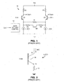
- Fig. 1 shows one type of conventional variable gain amplifier 10.
- FIG. 1 discloses a VGA as drawn in Fig. 1 .
- Fig. 1 differential input signals Vin+ and Vin- are applied to the transistors Q1 and Q2.
- Fixed current sources I_DC1 and I_DC2 couple the emitters of the transistors Q1 and Q2 to ground.
- a resistor R1 is coupled across the emitters to set a minimum gain of the amplifier.
- resistor R2 In parallel with resistor R1 are resistor R2, a MOSFET M1, and a resistor R3. When MOSFET M1 is off, the minimum gain is achieved. Progressively turning on MOSFET M1 increases the gain to a maximum.
- a V CTRL signal is converted to a proper level by a gate voltage control circuit 12.
- the currents through the transistors Q1 and Q2 cause voltage drops across the resistors R4 and R5, and the output of the amplifier may be the differential voltages Vout-and Vout+.
- headroom is the difference between the minimum input voltage Vin level needed for proper operation and Vcc (the operating voltage).
- Vcc the operating voltage
- Fig. 2 illustrates a very simple example of the current source I_DC1 or I_DC2 in Fig. 1 .
- a fixed bias voltage Vbias is coupled to the base of the bipolar transistor 14, and a degeneration resistor 16 is provided for improving the noise performance of the current source.
- the voltage drop across the resistor 16 may be 100mV.
- the collector-emitter voltage Vce may be a minimum of 0.4 volt. Therefore, the collector voltage must be at least 0.5 volt.
- the minimum level of Vin+ or Vin- must then be at least 1.2 volts, assuming a Vbe of the transistors Q1 and Q2 of 0.7 volt.
- Vcc must be high enough so that the Vce of the transistors Q1 and Q2 is sufficiently high for linear operation even with the highest currents across the transistors Q1 and Q2. As seen, due to the minimum operating requirements of the current sources I_DC1 and I_DC2, the minimum Vcc necessary to properly operate the amplifier 10 is limited.
- Vin+ and Vin- signals are generated by an upstream circuit, such as a digital-to-analog converter (DAC), the relatively high required minimum Vin+ and Vin-signals lower the headroom for those other circuits.
- an upstream circuit such as a digital-to-analog converter (DAC)
- DAC digital-to-analog converter
- variable gain amplifier that does not use an active current source between an input transistor and ground. Therefore, there is no current source that raises the required minimum input voltage level. As a result, headroom is increased, allowing the use of a lower minimum operating voltage Vcc.
- a VGA has differential (or complementary) inputs for receiving signals Vin+ and Vin-.
- Vin- is applied to the base of a bipolar first transistor whose emitter is coupled to ground via a first resistor and a MOSFET.
- the collector of the first transistor presents a current that may be used for any purpose, such as for modulating a carrier wave for RF transmission, or creating a voltage drop across an output resistor to generate an output voltage for any use.
- the conductivity of the MOSFET controls the trans-conductance gain of the first transistor.
- a bias voltage is externally supplied for setting a suitable gate bias range for the MOSFET.
- the Vin+ signal is applied to a bipolar second transistor, and the conductivity of the second transistor modulates the bias voltage applied to the MOSFET's gate.
- An increase in the Vin+ signal (while the Vin- signal decreases) lowers the gate voltage, which affects the conductivity of the MOSFET.
- the drain voltage of the MOSFET is modulated by the Vin- signal and thus undesirably generates distortion.
- the modulated gate voltage causes the AC component for a certain DC voltage at the drain of the MOSFET to be lowered, improving linearity.
- V DS AC voltage swing
- DC drain-source voltage V DS , DC
- the combined voltage drop across the first resistor and MOSFET can be made much lower than the required voltage drop across the current source I_DC1 of Fig. 1 so that the emitter voltage of the first transistor can be much lower. This results in increased headroom between Vin- and Vcc, allowing Vcc to be lower than the Vcc in Fig. 1 , while still achieving optimal operation of the amplifier. Allowing the minimum input signal Vin- to be lower also improves the headroom of the upstream circuits that generate Vin-.
- VGA Another advantage of the VGA is that the current consumption is lowered by the deletion of the two current sources, in case the gain setting is smaller than 0dB.
- a third advantage of the VGA is that it has better overall linearity due to the reduction of distortion by using a fraction of the input AC signal swing on the gate of the MOSFET.
- the single-ended amplifier may be made differential by interconnecting two of the amplifiers and reversing their input signals.
- the invention is particularly useful as an amplifier or mixer in an RF transmitter where digital signals are converted to an analog modulation signal for a carrier wave, such as in a QAM system.
- Various other embodiments are described that include a digital on-off circuit and a digital gain control for operation within various discrete gain ranges.
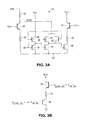
- Fig. 3A illustrates a first embodiment of a VGA 20 with increased headroom compared to the amplifier of Fig. 1 and with dynamic gain control for improving linearity.
- Differential analog signals Vin+ and Vin- are applied to the bases of transistors 22 and 24, respectively.
- the emitter of the transistor 24 is coupled to ground via a resistor 26 and an N-channel MOSFET 28.
- the output of the amplifier 20 is a variable current Iout through the collector of the transistor 24.
- the collector current may be directly coupled to the next stage, such as a mixer in a QAM modulator for a transmitter, or a resistor may be connected between the collector and Vcc, like in Fig. 1 , where the resulting voltage at the collector provides an output voltage to the next stage.
- the conductivity of the MOSFET 28 controls the gain of the amplifier 20.
- the transistor 22 has its emitter coupled to ground via a resistor 30 and its collector coupled to a gain control signal V CTRL via a resistor 32.
- V CTRL is a bias voltage that may be constant or varied by an external circuit and provides a bias voltage for the gate of the MOSFET 28. It is assumed that the signal V CTRL is constant during operation.
- the node between the resistor 32 and the collector of the transistor 22 provides a modulated control voltage V CTRL 2 to the gate of the MOSFET 28 via a digital on-off switch.
- the current through the transistor 22, controlled by the Vin+ signal, and the voltage drop across the resistor 32 are proportional to Vin-, such that the voltage applied to the gate of the MOSFET 28 can be considered to be a combined bias voltage and a signal proportional to Vin-.
- the proportionality depends on the gain of the transistor 22 and the value of the resistor 32.
- the digital signal b0 enables the amplifier 20 when high and disables the amplifier 20 when low.
- b0 is high, the N-channel MOSFET 34 is on and the P-channel MOSFET 36 is off. Therefore, the node 38 will be low.
- a pass gate is formed by parallel P-channel and N-channel MOSFETs 40 and 42, respectively.
- the low voltage at the node 38 turns the MOSFET 44 off and turns the MOSFET 40 on.
- the MOSFET 42 is also on by the high b0 signal. Since the V CTRL 2 signal is coupled to the conductive pass gate, the pass gate couples the V CTRL 2 signal directly to the gate of the MOSFET 28 to modulate the conductivity of the MOSFET 28.
- the transistor 22 draws more current and V CTRL 2 lowers. This lowers the MOSFET 28 gate voltage. At the same time, the lowered Vin- signal decreases the MOSFET's 28 drain voltage since R26 and MOSFET 28 form a voltage divider. At very low currents, the drain voltage of the MOSFET 28 may be about 0.6 volt. As the current through transistor 24 increases, the drain voltage is lowered.
- variable gain by controlling V CTRL , has a maximum range of about 70dB.
- the output of the amplifier 20 will be an output voltage at the collector of the transistor 24.
- the output of the amplifier 20 amplifies a signal to be transmitted, and the signal is mixed with a local oscillator signal or an RF signal for transmission.
- MOSFETs 40 and 42 in the pass gate are off.
- MOSFET 44 is on, connecting the gate of MOSFET 28 to ground and disabling the amplifier 20.
- the minimum level of the input voltage Vin- may be, for example, 0.7 volt or less, as compared with the minimum input voltage of 1.2 volt in Fig. 1 .
- the amplifier 20 may be operated with a lower operating voltage Vcc.
- Equation (1) W L ⁇ ⁇ ⁇ C OX ⁇ ⁇ V GS - V T ⁇ V DS - 1 2 ⁇ V DS 2 with I D being the drain current, V GS the gate-source voltage, V T the threshold voltage, V DS the drain-source voltage, W the width of the MOSFET, L the length of the MOSFET, ⁇ the electron mobility and C' OX the gate capacitance per unit area. Equation (1) is valid for V GS > V DS + V T , the so-called "triode" region. Equation (1) predicts second-order distortion because of the V DS 2 term. In a balanced configuration, the even-order contributions will largely cancel and no other distortion products will be present according to Equation (1).
- Equation (2) It seems the insight from Equation (2) is not much more than using the MOSFET models themselves as a basis to explain the third-order distortion effects.
- MOSFET 28 is controlling the variable gain aspect of Fig. 3 .
- the equivalent output resistance of MOSFET 28 seen at the drain is not only determined by the current increase caused by a drain-source voltage increase (dI D /dV DS ) but now also by a current increase caused by an increasing gate-source voltage (dI D /dV GS ).
- V CTRL sets the gate-source DC bias point (V GS, DC ) and as a result shifts the drain-source bias point (V DS, DC ) also. This shifts the contribution the gate-source AC voltage swing and the drain-source AC voltage swing have on the dynamic resistance at the drain.
- V CTRL For maximum gain (V CTRL is high, 0dB gain) the trans-conductance from the gate (dI D /dV GS ) is low compared to the trans-conductance from the drain (dI D /dV DS ). For much lower gain settings (say -10dB gain), the opposite happens. In between, both contributions can be equal (which happens for gain setting of about -2dB in our implementation).
- All components of the converter may be formed in a single integrated circuit.
- Fig. 3B illustrates the output portion of the VGA of Fig. 3A with the control signals identified.
- the control input into the gate of the MOSFET 28 can be considered to be the DC V CTRL signal modulated by a signal proportional to Vin-.
- the base voltage into the transistor 24 is a DC bias voltage V BIAS, DC (for establishing an operating point) plus the Vin-signal. Vin- is assumed to be an AC signal.
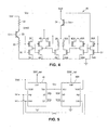
- Fig. 4 illustrates the amplifier 20 of Fig. 3 but with the gain being further controlled by the digital signals b0 and b1.
- the value of the resistor 26A is twice that of resistor 26, and the MOSFET 28 is twice as wide as the MOSFET 28A.
- the other components 34A, 36A, 40A, 42A, and 44A in the digital switch may be identical to the components 34, 36, 40, 42, and 44.
- the four gain settings produce a maximum trans-conductance gain of 0, 1/resistor 26, 1/resistor 26A, and 1/resistor 26 in parallel with resistor 26A.
- the MOSFET 28 and 28A conductivities are controlled by V CTRL 2, which are modulated by the Vin+ signal, as previously described, to improve the linearity.
- the effects of the MOSFETs 28 and 28A lower the maximum gains set by the signals b0 and b1 down to a value that can be 70dB lower.
- the amplifier 46 of Fig. 4 has a single-ended output Iout. If a differential output is desired, the configuration of Fig. 5 may be used, where two identical amplifiers 46 and 46A are used and the inputs to the amplifiers 46 and 46A are reversed. Identical b0 and b1 signals are applied to the terminals of both amplifiers 46 and 46A. In Fig. 5 , it is assumed that the outputs are differential baseband outputs BBP_out and BBM_out for a transmitter. These signals may then be applied to a differential mixer for modulating an LO carrier wave with the baseband signal. The baseband signal may represent a voice signal, a digital code, or any other signal for RF transmission. Any AC currents in the V CTRL signal will be opposite in phase for the two amplifiers and will cancel out, and only a DC current remains.
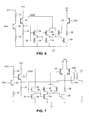
- Fig. 6 is identical to Fig. 3A except a level shifter, formed by transistor 50 and resistor 52, level shifts the V CTRL 2 signal downward by about 0.7 volt to prevent transistor 22going into saturation in case MOSFET 28 is set to a low gate voltage. Additional level shifting circuits may also be used to adjust the range of the gate voltage. Resistor 52 may have a series MOSFET to disable the current in transistor 50 when the circuit is switched off.
- Fig. 7 illustrates the VGA of Fig. 6 but where the input signal Vin- is applied to a center tap of a transformer T1 to create a differential signal applied to the transistors 24A and 24B.
- a local oscillator LO signal (e.g., 500MHz) is applied to a secondary winding of the transformer T1 to multiply the modulating signal by the LO signal.
- the differential signal at the output of the transistors 24A and 24B may then be applied to a power amplifier for RF transmission.
- OIP3 is the output third order intercept point, based on third-order inter-modulation products (IM3), and plotting the OIP3 versus various values is a common way for designers to measure the performance of a transmitter.
- IM3 third-order inter-modulation products
- the simplified results are shown in the graph of Fig. 8 .
- An ideal OIP3 value would track the solid line representing constant power difference between IM3 products and desired signal vs. gain setting.
- the graph shows much more linear operation with the transistor 22 connected versus when the transistor 22 is disconnected.
- Fig. 9 illustrates a single IC 56 that is a quadrature modulator, whose differential amplifier 58and mixer 62, is identical to the amplifier/mixer of Fig. 7 expanded in a differential fashion like Fig. 5 .
- This is doubled to create I and Q paths depicted as amplifiers 58, 60 and mixers 62, 64.
- Differential baseband signals BBPI, BBMI, BBPQ, and BBMQ are applied to the inputs of the amplifiers 58 and 60, where the positive input corresponds to the Vin+ signal and the negative input corresponds to the Vin- signal.
- Mixers 62 and 64 mix the amplified signals with differential LO signals (90° out of phase) to generate the I and Q signals for transmission.
- An RF buffer 70 converts the differential output to a single ended output for RF transmission.
- the AC Gate-Source voltage swing divided by the input signal AC voltage swing is called ⁇ .
- the VGA gain values from -10dB to 0dB in 1dB steps are indicated in the graph (with 0dB normalized to the maximum gain setting).
- the gain is decreased from 0dB to -10dB, the AC voltage swing on the MOSFET 28 drain is increased significantly and is causing the dominant source of distortion.
- V DS AC voltage swing
- V DS, DC DC drain-source voltage
- the inter-modulation distortion is derived by multiplying the third-order derivative of I D vs V DS (notation: d 3 I D /dV DS 3 ) with the qubic voltage swing (v DS 3 ).
- the scaling factor can be derived from equations 3, 4 and 5 using the Taylor expansion and goniometric formulas.
- OIP3 Output Third-Order Intercept Point
- Vin+ and Vin- signals may be reversed.
- transistors may be all MOSFETs.
- the MOSFETs shown as NMOS transistors may be switched with PMOS transistors and vice versa, and the NPN transistors can be switched with PNP transistors, also making Vcc negative while it is assumed positive in the figures.
Landscapes
- Engineering & Computer Science (AREA)
- Power Engineering (AREA)
- Computer Networks & Wireless Communication (AREA)
- Signal Processing (AREA)
- Physics & Mathematics (AREA)
- Nonlinear Science (AREA)
- Amplifiers (AREA)
- Control Of Amplification And Gain Control (AREA)
Applications Claiming Priority (2)
| Application Number | Priority Date | Filing Date | Title |
|---|---|---|---|
| US201461989908P | 2014-05-07 | 2014-05-07 | |
| US14/670,031 US9391577B2 (en) | 2014-05-07 | 2015-03-26 | Low-voltage analog variable gain amplifier with enhanced linearity |
Publications (3)
| Publication Number | Publication Date |
|---|---|
| EP2942869A2 true EP2942869A2 (de) | 2015-11-11 |
| EP2942869A3 EP2942869A3 (de) | 2015-12-09 |
| EP2942869B1 EP2942869B1 (de) | 2020-10-28 |
Family
ID=53002470
Family Applications (1)
| Application Number | Title | Priority Date | Filing Date |
|---|---|---|---|
| EP15001197.1A Active EP2942869B1 (de) | 2014-05-07 | 2015-04-22 | Analoger variabler niederspannungsleistungsverstärker mit verbesserter linearität |
Country Status (3)
| Country | Link |
|---|---|
| US (1) | US9391577B2 (de) |
| EP (1) | EP2942869B1 (de) |
| TW (1) | TWI571051B (de) |
Cited By (1)
| Publication number | Priority date | Publication date | Assignee | Title |
|---|---|---|---|---|
| CN109150112A (zh) * | 2018-08-01 | 2019-01-04 | 电子科技大学 | 超宽带可变增益混频器 |
Families Citing this family (6)
| Publication number | Priority date | Publication date | Assignee | Title |
|---|---|---|---|---|
| CN113810000A (zh) | 2016-05-12 | 2021-12-17 | 华为技术有限公司 | 含压降元件的电路 |
| WO2018075599A1 (en) | 2016-10-18 | 2018-04-26 | Carrier Corporation | Flame scanner having non-linear amplifier with temperature compensation |
| US10848109B2 (en) | 2017-01-26 | 2020-11-24 | Analog Devices, Inc. | Bias modulation active linearization for broadband amplifiers |
| US10374092B2 (en) | 2017-04-17 | 2019-08-06 | Globalfoundries Inc. | Power amplifier ramping and power control with forward and reverse back-gate bias |
| US11128499B2 (en) | 2018-04-18 | 2021-09-21 | Rambus Inc. | Serial-link receiver using time-interleaved discrete time gain |
| US12489443B2 (en) * | 2022-10-12 | 2025-12-02 | Xilinx, Inc. | Low power driver scheme for on-chip and interposer based data transmission |
Citations (1)
| Publication number | Priority date | Publication date | Assignee | Title |
|---|---|---|---|---|
| US7889006B1 (en) | 2009-09-23 | 2011-02-15 | Maxim Integrated Products, Inc. | dB-linear process-independent variable gain amplifier |
Family Cites Families (9)
| Publication number | Priority date | Publication date | Assignee | Title |
|---|---|---|---|---|
| US4081609A (en) * | 1977-01-28 | 1978-03-28 | Reliance Telecommunication Electronics Company | Synchronous ring detector for station carrier telephone systems |
| US4495470A (en) * | 1983-02-07 | 1985-01-22 | Tektronix, Inc. | Offset balancing method and apparatus for a DC amplifier |
| US5724519A (en) * | 1989-02-17 | 1998-03-03 | Hitachi, Ltd. | Complementary transistor circuit and amplifier and CRT display device using the same |
| WO1998059416A1 (en) | 1997-06-25 | 1998-12-30 | Koninklijke Philips Electronics N.V. | A differential amplifier, an integrated circuit, and a telephone |
| US6218902B1 (en) | 1999-04-20 | 2001-04-17 | Nortel Networks Limited | Wide-band linearization technique |
| JP2001274641A (ja) | 2000-03-27 | 2001-10-05 | Toshiba Corp | 差動増幅器及びこれを用いたフィルタ回路 |
| FR2872648B1 (fr) | 2004-06-30 | 2006-09-08 | St Microelectronics Sa | Amplificateur a transconductance rapide |
| US7741909B2 (en) | 2008-04-14 | 2010-06-22 | Mediatek Singapore Pte Ltd | Linear-in-dB variable gain amplifier |
| JP5308243B2 (ja) * | 2009-06-10 | 2013-10-09 | 株式会社日立製作所 | 可変ゲイン回路 |
-
2015
- 2015-03-26 US US14/670,031 patent/US9391577B2/en active Active
- 2015-04-22 EP EP15001197.1A patent/EP2942869B1/de active Active
- 2015-04-24 TW TW104113315A patent/TWI571051B/zh active
Patent Citations (1)
| Publication number | Priority date | Publication date | Assignee | Title |
|---|---|---|---|---|
| US7889006B1 (en) | 2009-09-23 | 2011-02-15 | Maxim Integrated Products, Inc. | dB-linear process-independent variable gain amplifier |
Cited By (1)
| Publication number | Priority date | Publication date | Assignee | Title |
|---|---|---|---|---|
| CN109150112A (zh) * | 2018-08-01 | 2019-01-04 | 电子科技大学 | 超宽带可变增益混频器 |
Also Published As
| Publication number | Publication date |
|---|---|
| TW201545472A (zh) | 2015-12-01 |
| US9391577B2 (en) | 2016-07-12 |
| EP2942869B1 (de) | 2020-10-28 |
| US20150326198A1 (en) | 2015-11-12 |
| EP2942869A3 (de) | 2015-12-09 |
| TWI571051B (zh) | 2017-02-11 |
Similar Documents
| Publication | Publication Date | Title |
|---|---|---|
| EP2942869B1 (de) | Analoger variabler niederspannungsleistungsverstärker mit verbesserter linearität | |
| US4814649A (en) | Dual gate FET mixing apparatus with feedback means | |
| US8841968B2 (en) | Class-AB radio frequency amplifier for envelope detector | |
| US7679448B1 (en) | Continuous wave based bias method and apparatus for minimizing MOS transistor distortion | |
| US9178476B2 (en) | Envelope detector with enhanced linear range | |
| US20110050319A1 (en) | Multiplier, Mixer, Modulator, Receiver and Transmitter | |
| US8471637B2 (en) | Variable gain amplifier | |
| KR20020035324A (ko) | 차동 증폭기 | |
| CN107994897B (zh) | 一种偏置电流控制电路、方法以及功率放大控制电路 | |
| US7777575B2 (en) | Circuit with single-ended input and differential output | |
| CN101542896A (zh) | 混频器 | |
| JP2017079447A (ja) | 駆動回路及び可変利得増幅器 | |
| US20100001797A1 (en) | Differential amplifier | |
| JP2009534957A (ja) | 併合型の混合器及び可変利得増幅器を備える温度補償されたcmos送信回路 | |
| CN115606100B (zh) | 射频调制器装置 | |
| US7446608B2 (en) | Variable gain amplifier with constant input referred third order intercept | |
| KR101013382B1 (ko) | 주파수 혼합기 | |
| US7106606B2 (en) | Voltage-current converter with adjustable quiescent current | |
| US7426372B2 (en) | Piecewise linearizer circuit for radio frequency amplification | |
| US7821342B2 (en) | Device comprising a feedback-less gain controlled amplifier | |
| US7342432B2 (en) | Mixer circuit having improved linearity and noise figure | |
| US20080315953A1 (en) | Variable Gain Mixer | |
| Ananda et al. | A Wide Tuning Range and Low Power RF Filter for Wireless Local Area Network Applications | |
| KR20150055347A (ko) | 디지털 바이어스 회로를 이용한 디지털 rf 전력 증폭기 장치 | |
| JP2006295374A (ja) | 増幅回路、電圧電流変換回路および送信装置 |
Legal Events
| Date | Code | Title | Description |
|---|---|---|---|
| PUAL | Search report despatched |
Free format text: ORIGINAL CODE: 0009013 |
|
| PUAI | Public reference made under article 153(3) epc to a published international application that has entered the european phase |
Free format text: ORIGINAL CODE: 0009012 |
|
| AK | Designated contracting states |
Kind code of ref document: A2 Designated state(s): AL AT BE BG CH CY CZ DE DK EE ES FI FR GB GR HR HU IE IS IT LI LT LU LV MC MK MT NL NO PL PT RO RS SE SI SK SM TR |
|
| AX | Request for extension of the european patent |
Extension state: BA ME |
|
| AK | Designated contracting states |
Kind code of ref document: A3 Designated state(s): AL AT BE BG CH CY CZ DE DK EE ES FI FR GB GR HR HU IE IS IT LI LT LU LV MC MK MT NL NO PL PT RO RS SE SI SK SM TR |
|
| AX | Request for extension of the european patent |
Extension state: BA ME |
|
| RIC1 | Information provided on ipc code assigned before grant |
Ipc: H03F 1/32 20060101AFI20151105BHEP Ipc: H03G 1/00 20060101ALI20151105BHEP |
|
| 17P | Request for examination filed |
Effective date: 20160607 |
|
| RBV | Designated contracting states (corrected) |
Designated state(s): AL AT BE BG CH CY CZ DE DK EE ES FI FR GB GR HR HU IE IS IT LI LT LU LV MC MK MT NL NO PL PT RO RS SE SI SK SM TR |
|
| STAA | Information on the status of an ep patent application or granted ep patent |
Free format text: STATUS: EXAMINATION IS IN PROGRESS |
|
| 17Q | First examination report despatched |
Effective date: 20180302 |
|
| GRAJ | Information related to disapproval of communication of intention to grant by the applicant or resumption of examination proceedings by the epo deleted |
Free format text: ORIGINAL CODE: EPIDOSDIGR1 |
|
| STAA | Information on the status of an ep patent application or granted ep patent |
Free format text: STATUS: GRANT OF PATENT IS INTENDED |
|
| GRAP | Despatch of communication of intention to grant a patent |
Free format text: ORIGINAL CODE: EPIDOSNIGR1 |
|
| RIC1 | Information provided on ipc code assigned before grant |
Ipc: H03F 1/02 20060101ALI20200327BHEP Ipc: H04L 27/36 20060101ALI20200327BHEP Ipc: H03G 1/00 20060101ALI20200327BHEP Ipc: H03F 3/45 20060101ALI20200327BHEP Ipc: H03F 1/32 20060101AFI20200327BHEP Ipc: H03F 3/19 20060101ALI20200327BHEP |
|
| INTG | Intention to grant announced |
Effective date: 20200506 |
|
| GRAS | Grant fee paid |
Free format text: ORIGINAL CODE: EPIDOSNIGR3 |
|
| GRAA | (expected) grant |
Free format text: ORIGINAL CODE: 0009210 |
|
| STAA | Information on the status of an ep patent application or granted ep patent |
Free format text: STATUS: THE PATENT HAS BEEN GRANTED |
|
| AK | Designated contracting states |
Kind code of ref document: B1 Designated state(s): AL AT BE BG CH CY CZ DE DK EE ES FI FR GB GR HR HU IE IS IT LI LT LU LV MC MK MT NL NO PL PT RO RS SE SI SK SM TR |
|
| RAP1 | Party data changed (applicant data changed or rights of an application transferred) |
Owner name: ANALOG DEVICES INTERNATIONAL UNLIMITED COMPANY |
|
| REG | Reference to a national code |
Ref country code: GB Ref legal event code: FG4D |
|
| REG | Reference to a national code |
Ref country code: CH Ref legal event code: EP |
|
| REG | Reference to a national code |
Ref country code: DE Ref legal event code: R096 Ref document number: 602015061011 Country of ref document: DE |
|
| REG | Reference to a national code |
Ref country code: AT Ref legal event code: REF Ref document number: 1329257 Country of ref document: AT Kind code of ref document: T Effective date: 20201115 |
|
| REG | Reference to a national code |
Ref country code: IE Ref legal event code: FG4D |
|
| REG | Reference to a national code |
Ref country code: AT Ref legal event code: MK05 Ref document number: 1329257 Country of ref document: AT Kind code of ref document: T Effective date: 20201028 |
|
| REG | Reference to a national code |
Ref country code: NL Ref legal event code: MP Effective date: 20201028 |
|
| PG25 | Lapsed in a contracting state [announced via postgrant information from national office to epo] |
Ref country code: GR Free format text: LAPSE BECAUSE OF FAILURE TO SUBMIT A TRANSLATION OF THE DESCRIPTION OR TO PAY THE FEE WITHIN THE PRESCRIBED TIME-LIMIT Effective date: 20210129 Ref country code: FI Free format text: LAPSE BECAUSE OF FAILURE TO SUBMIT A TRANSLATION OF THE DESCRIPTION OR TO PAY THE FEE WITHIN THE PRESCRIBED TIME-LIMIT Effective date: 20201028 Ref country code: RS Free format text: LAPSE BECAUSE OF FAILURE TO SUBMIT A TRANSLATION OF THE DESCRIPTION OR TO PAY THE FEE WITHIN THE PRESCRIBED TIME-LIMIT Effective date: 20201028 Ref country code: NO Free format text: LAPSE BECAUSE OF FAILURE TO SUBMIT A TRANSLATION OF THE DESCRIPTION OR TO PAY THE FEE WITHIN THE PRESCRIBED TIME-LIMIT Effective date: 20210128 Ref country code: NL Free format text: LAPSE BECAUSE OF FAILURE TO SUBMIT A TRANSLATION OF THE DESCRIPTION OR TO PAY THE FEE WITHIN THE PRESCRIBED TIME-LIMIT Effective date: 20201028 Ref country code: PT Free format text: LAPSE BECAUSE OF FAILURE TO SUBMIT A TRANSLATION OF THE DESCRIPTION OR TO PAY THE FEE WITHIN THE PRESCRIBED TIME-LIMIT Effective date: 20210301 |
|
| REG | Reference to a national code |
Ref country code: LT Ref legal event code: MG4D |
|
| PG25 | Lapsed in a contracting state [announced via postgrant information from national office to epo] |
Ref country code: BG Free format text: LAPSE BECAUSE OF FAILURE TO SUBMIT A TRANSLATION OF THE DESCRIPTION OR TO PAY THE FEE WITHIN THE PRESCRIBED TIME-LIMIT Effective date: 20210128 Ref country code: ES Free format text: LAPSE BECAUSE OF FAILURE TO SUBMIT A TRANSLATION OF THE DESCRIPTION OR TO PAY THE FEE WITHIN THE PRESCRIBED TIME-LIMIT Effective date: 20201028 Ref country code: AT Free format text: LAPSE BECAUSE OF FAILURE TO SUBMIT A TRANSLATION OF THE DESCRIPTION OR TO PAY THE FEE WITHIN THE PRESCRIBED TIME-LIMIT Effective date: 20201028 Ref country code: SE Free format text: LAPSE BECAUSE OF FAILURE TO SUBMIT A TRANSLATION OF THE DESCRIPTION OR TO PAY THE FEE WITHIN THE PRESCRIBED TIME-LIMIT Effective date: 20201028 Ref country code: PL Free format text: LAPSE BECAUSE OF FAILURE TO SUBMIT A TRANSLATION OF THE DESCRIPTION OR TO PAY THE FEE WITHIN THE PRESCRIBED TIME-LIMIT Effective date: 20201028 Ref country code: LV Free format text: LAPSE BECAUSE OF FAILURE TO SUBMIT A TRANSLATION OF THE DESCRIPTION OR TO PAY THE FEE WITHIN THE PRESCRIBED TIME-LIMIT Effective date: 20201028 Ref country code: IS Free format text: LAPSE BECAUSE OF FAILURE TO SUBMIT A TRANSLATION OF THE DESCRIPTION OR TO PAY THE FEE WITHIN THE PRESCRIBED TIME-LIMIT Effective date: 20210228 |
|
| PG25 | Lapsed in a contracting state [announced via postgrant information from national office to epo] |
Ref country code: HR Free format text: LAPSE BECAUSE OF FAILURE TO SUBMIT A TRANSLATION OF THE DESCRIPTION OR TO PAY THE FEE WITHIN THE PRESCRIBED TIME-LIMIT Effective date: 20201028 |
|
| REG | Reference to a national code |
Ref country code: DE Ref legal event code: R097 Ref document number: 602015061011 Country of ref document: DE |
|
| PG25 | Lapsed in a contracting state [announced via postgrant information from national office to epo] |
Ref country code: SM Free format text: LAPSE BECAUSE OF FAILURE TO SUBMIT A TRANSLATION OF THE DESCRIPTION OR TO PAY THE FEE WITHIN THE PRESCRIBED TIME-LIMIT Effective date: 20201028 Ref country code: CZ Free format text: LAPSE BECAUSE OF FAILURE TO SUBMIT A TRANSLATION OF THE DESCRIPTION OR TO PAY THE FEE WITHIN THE PRESCRIBED TIME-LIMIT Effective date: 20201028 Ref country code: EE Free format text: LAPSE BECAUSE OF FAILURE TO SUBMIT A TRANSLATION OF THE DESCRIPTION OR TO PAY THE FEE WITHIN THE PRESCRIBED TIME-LIMIT Effective date: 20201028 Ref country code: SK Free format text: LAPSE BECAUSE OF FAILURE TO SUBMIT A TRANSLATION OF THE DESCRIPTION OR TO PAY THE FEE WITHIN THE PRESCRIBED TIME-LIMIT Effective date: 20201028 Ref country code: RO Free format text: LAPSE BECAUSE OF FAILURE TO SUBMIT A TRANSLATION OF THE DESCRIPTION OR TO PAY THE FEE WITHIN THE PRESCRIBED TIME-LIMIT Effective date: 20201028 Ref country code: LT Free format text: LAPSE BECAUSE OF FAILURE TO SUBMIT A TRANSLATION OF THE DESCRIPTION OR TO PAY THE FEE WITHIN THE PRESCRIBED TIME-LIMIT Effective date: 20201028 |
|
| PG25 | Lapsed in a contracting state [announced via postgrant information from national office to epo] |
Ref country code: DK Free format text: LAPSE BECAUSE OF FAILURE TO SUBMIT A TRANSLATION OF THE DESCRIPTION OR TO PAY THE FEE WITHIN THE PRESCRIBED TIME-LIMIT Effective date: 20201028 |
|
| PLBE | No opposition filed within time limit |
Free format text: ORIGINAL CODE: 0009261 |
|
| STAA | Information on the status of an ep patent application or granted ep patent |
Free format text: STATUS: NO OPPOSITION FILED WITHIN TIME LIMIT |
|
| 26N | No opposition filed |
Effective date: 20210729 |
|
| PG25 | Lapsed in a contracting state [announced via postgrant information from national office to epo] |
Ref country code: AL Free format text: LAPSE BECAUSE OF FAILURE TO SUBMIT A TRANSLATION OF THE DESCRIPTION OR TO PAY THE FEE WITHIN THE PRESCRIBED TIME-LIMIT Effective date: 20201028 Ref country code: IT Free format text: LAPSE BECAUSE OF FAILURE TO SUBMIT A TRANSLATION OF THE DESCRIPTION OR TO PAY THE FEE WITHIN THE PRESCRIBED TIME-LIMIT Effective date: 20201028 |
|
| PGFP | Annual fee paid to national office [announced via postgrant information from national office to epo] |
Ref country code: IE Payment date: 20210707 Year of fee payment: 7 |
|
| PG25 | Lapsed in a contracting state [announced via postgrant information from national office to epo] |
Ref country code: SI Free format text: LAPSE BECAUSE OF FAILURE TO SUBMIT A TRANSLATION OF THE DESCRIPTION OR TO PAY THE FEE WITHIN THE PRESCRIBED TIME-LIMIT Effective date: 20201028 Ref country code: MC Free format text: LAPSE BECAUSE OF FAILURE TO SUBMIT A TRANSLATION OF THE DESCRIPTION OR TO PAY THE FEE WITHIN THE PRESCRIBED TIME-LIMIT Effective date: 20201028 |
|
| PG25 | Lapsed in a contracting state [announced via postgrant information from national office to epo] |
Ref country code: LU Free format text: LAPSE BECAUSE OF NON-PAYMENT OF DUE FEES Effective date: 20210422 |
|
| REG | Reference to a national code |
Ref country code: BE Ref legal event code: MM Effective date: 20210430 |
|
| PG25 | Lapsed in a contracting state [announced via postgrant information from national office to epo] |
Ref country code: LI Free format text: LAPSE BECAUSE OF NON-PAYMENT OF DUE FEES Effective date: 20210430 Ref country code: CH Free format text: LAPSE BECAUSE OF NON-PAYMENT OF DUE FEES Effective date: 20210430 |
|
| PG25 | Lapsed in a contracting state [announced via postgrant information from national office to epo] |
Ref country code: IS Free format text: LAPSE BECAUSE OF FAILURE TO SUBMIT A TRANSLATION OF THE DESCRIPTION OR TO PAY THE FEE WITHIN THE PRESCRIBED TIME-LIMIT Effective date: 20210228 |
|
| PG25 | Lapsed in a contracting state [announced via postgrant information from national office to epo] |
Ref country code: BE Free format text: LAPSE BECAUSE OF NON-PAYMENT OF DUE FEES Effective date: 20210430 |
|
| PG25 | Lapsed in a contracting state [announced via postgrant information from national office to epo] |
Ref country code: IE Free format text: LAPSE BECAUSE OF NON-PAYMENT OF DUE FEES Effective date: 20220422 |
|
| PG25 | Lapsed in a contracting state [announced via postgrant information from national office to epo] |
Ref country code: HU Free format text: LAPSE BECAUSE OF FAILURE TO SUBMIT A TRANSLATION OF THE DESCRIPTION OR TO PAY THE FEE WITHIN THE PRESCRIBED TIME-LIMIT; INVALID AB INITIO Effective date: 20150422 |
|
| PG25 | Lapsed in a contracting state [announced via postgrant information from national office to epo] |
Ref country code: CY Free format text: LAPSE BECAUSE OF FAILURE TO SUBMIT A TRANSLATION OF THE DESCRIPTION OR TO PAY THE FEE WITHIN THE PRESCRIBED TIME-LIMIT Effective date: 20201028 |
|
| PG25 | Lapsed in a contracting state [announced via postgrant information from national office to epo] |
Ref country code: MK Free format text: LAPSE BECAUSE OF FAILURE TO SUBMIT A TRANSLATION OF THE DESCRIPTION OR TO PAY THE FEE WITHIN THE PRESCRIBED TIME-LIMIT Effective date: 20201028 |
|
| PG25 | Lapsed in a contracting state [announced via postgrant information from national office to epo] |
Ref country code: MT Free format text: LAPSE BECAUSE OF FAILURE TO SUBMIT A TRANSLATION OF THE DESCRIPTION OR TO PAY THE FEE WITHIN THE PRESCRIBED TIME-LIMIT Effective date: 20201028 |
|
| PGFP | Annual fee paid to national office [announced via postgrant information from national office to epo] |
Ref country code: DE Payment date: 20250319 Year of fee payment: 11 |
|
| PG25 | Lapsed in a contracting state [announced via postgrant information from national office to epo] |
Ref country code: TR Free format text: LAPSE BECAUSE OF FAILURE TO SUBMIT A TRANSLATION OF THE DESCRIPTION OR TO PAY THE FEE WITHIN THE PRESCRIBED TIME-LIMIT Effective date: 20201028 |
|
| PGFP | Annual fee paid to national office [announced via postgrant information from national office to epo] |
Ref country code: GB Payment date: 20260319 Year of fee payment: 12 |
|
| PGFP | Annual fee paid to national office [announced via postgrant information from national office to epo] |
Ref country code: FR Payment date: 20260319 Year of fee payment: 12 |