EP2934075A1 - Multilayer wiring substrate and production method therefor - Google Patents
Multilayer wiring substrate and production method therefor Download PDFInfo
- Publication number
- EP2934075A1 EP2934075A1 EP13862412.7A EP13862412A EP2934075A1 EP 2934075 A1 EP2934075 A1 EP 2934075A1 EP 13862412 A EP13862412 A EP 13862412A EP 2934075 A1 EP2934075 A1 EP 2934075A1
- Authority
- EP
- European Patent Office
- Prior art keywords
- electronic component
- layered structure
- insulation layer
- layer
- wiring substrate
- Prior art date
- Legal status (The legal status is an assumption and is not a legal conclusion. Google has not performed a legal analysis and makes no representation as to the accuracy of the status listed.)
- Withdrawn
Links
Images







Classifications
-
- H—ELECTRICITY
- H05—ELECTRIC TECHNIQUES NOT OTHERWISE PROVIDED FOR
- H05K—PRINTED CIRCUITS; CASINGS OR CONSTRUCTIONAL DETAILS OF ELECTRIC APPARATUS; MANUFACTURE OF ASSEMBLAGES OF ELECTRICAL COMPONENTS
- H05K1/00—Printed circuits
- H05K1/18—Printed circuits structurally associated with non-printed electric components
- H05K1/182—Printed circuits structurally associated with non-printed electric components associated with components mounted in printed circuit boards [PCB], e.g. insert-mounted components [IMC]
- H05K1/185—Printed circuits structurally associated with non-printed electric components associated with components mounted in printed circuit boards [PCB], e.g. insert-mounted components [IMC] associated with components encapsulated in the insulating substrate of the PCBs; associated with components incorporated in internal layers of multilayer circuit boards
-
- H—ELECTRICITY
- H05—ELECTRIC TECHNIQUES NOT OTHERWISE PROVIDED FOR
- H05K—PRINTED CIRCUITS; CASINGS OR CONSTRUCTIONAL DETAILS OF ELECTRIC APPARATUS; MANUFACTURE OF ASSEMBLAGES OF ELECTRICAL COMPONENTS
- H05K1/00—Printed circuits
- H05K1/02—Details
- H05K1/0296—Conductive pattern lay-out details not covered by sub groups H05K1/02 - H05K1/0295
- H05K1/0298—Multilayer circuits
-
- H—ELECTRICITY
- H05—ELECTRIC TECHNIQUES NOT OTHERWISE PROVIDED FOR
- H05K—PRINTED CIRCUITS; CASINGS OR CONSTRUCTIONAL DETAILS OF ELECTRIC APPARATUS; MANUFACTURE OF ASSEMBLAGES OF ELECTRICAL COMPONENTS
- H05K1/00—Printed circuits
- H05K1/02—Details
- H05K1/11—Printed elements for providing electric connections to or between printed circuits
- H05K1/115—Via connections; Lands around holes or via connections
-
- H—ELECTRICITY
- H05—ELECTRIC TECHNIQUES NOT OTHERWISE PROVIDED FOR
- H05K—PRINTED CIRCUITS; CASINGS OR CONSTRUCTIONAL DETAILS OF ELECTRIC APPARATUS; MANUFACTURE OF ASSEMBLAGES OF ELECTRICAL COMPONENTS
- H05K1/00—Printed circuits
- H05K1/18—Printed circuits structurally associated with non-printed electric components
- H05K1/182—Printed circuits structurally associated with non-printed electric components associated with components mounted in printed circuit boards [PCB], e.g. insert-mounted components [IMC]
-
- H—ELECTRICITY
- H05—ELECTRIC TECHNIQUES NOT OTHERWISE PROVIDED FOR
- H05K—PRINTED CIRCUITS; CASINGS OR CONSTRUCTIONAL DETAILS OF ELECTRIC APPARATUS; MANUFACTURE OF ASSEMBLAGES OF ELECTRICAL COMPONENTS
- H05K3/00—Apparatus or processes for manufacturing printed circuits
- H05K3/30—Assembling printed circuits with electric components, e.g. with resistors
-
- H—ELECTRICITY
- H05—ELECTRIC TECHNIQUES NOT OTHERWISE PROVIDED FOR
- H05K—PRINTED CIRCUITS; CASINGS OR CONSTRUCTIONAL DETAILS OF ELECTRIC APPARATUS; MANUFACTURE OF ASSEMBLAGES OF ELECTRICAL COMPONENTS
- H05K3/00—Apparatus or processes for manufacturing printed circuits
- H05K3/40—Forming printed elements for providing electric connections to or between printed circuits
- H05K3/42—Plated through-holes or plated via connections
- H05K3/429—Plated through-holes specially for multilayer circuits, e.g. having connections to inner circuit layers
-
- H—ELECTRICITY
- H05—ELECTRIC TECHNIQUES NOT OTHERWISE PROVIDED FOR
- H05K—PRINTED CIRCUITS; CASINGS OR CONSTRUCTIONAL DETAILS OF ELECTRIC APPARATUS; MANUFACTURE OF ASSEMBLAGES OF ELECTRICAL COMPONENTS
- H05K3/00—Apparatus or processes for manufacturing printed circuits
- H05K3/46—Manufacturing multilayer circuits
- H05K3/4644—Manufacturing multilayer circuits by building the multilayer layer by layer, i.e. build-up multilayer circuits
- H05K3/4647—Manufacturing multilayer circuits by building the multilayer layer by layer, i.e. build-up multilayer circuits by applying an insulating layer around previously made via studs
-
- H—ELECTRICITY
- H05—ELECTRIC TECHNIQUES NOT OTHERWISE PROVIDED FOR
- H05K—PRINTED CIRCUITS; CASINGS OR CONSTRUCTIONAL DETAILS OF ELECTRIC APPARATUS; MANUFACTURE OF ASSEMBLAGES OF ELECTRICAL COMPONENTS
- H05K3/00—Apparatus or processes for manufacturing printed circuits
- H05K3/46—Manufacturing multilayer circuits
- H05K3/4644—Manufacturing multilayer circuits by building the multilayer layer by layer, i.e. build-up multilayer circuits
- H05K3/4682—Manufacture of core-less build-up multilayer circuits on a temporary carrier or on a metal foil
-
- H—ELECTRICITY
- H05—ELECTRIC TECHNIQUES NOT OTHERWISE PROVIDED FOR
- H05K—PRINTED CIRCUITS; CASINGS OR CONSTRUCTIONAL DETAILS OF ELECTRIC APPARATUS; MANUFACTURE OF ASSEMBLAGES OF ELECTRICAL COMPONENTS
- H05K1/00—Printed circuits
- H05K1/18—Printed circuits structurally associated with non-printed electric components
- H05K1/182—Printed circuits structurally associated with non-printed electric components associated with components mounted in printed circuit boards [PCB], e.g. insert-mounted components [IMC]
- H05K1/185—Printed circuits structurally associated with non-printed electric components associated with components mounted in printed circuit boards [PCB], e.g. insert-mounted components [IMC] associated with components encapsulated in the insulating substrate of the PCBs; associated with components incorporated in internal layers of multilayer circuit boards
- H05K1/186—Printed circuits structurally associated with non-printed electric components associated with components mounted in printed circuit boards [PCB], e.g. insert-mounted components [IMC] associated with components encapsulated in the insulating substrate of the PCBs; associated with components incorporated in internal layers of multilayer circuit boards manufactured by mounting on or connecting to patterned circuits before or during embedding
-
- H—ELECTRICITY
- H05—ELECTRIC TECHNIQUES NOT OTHERWISE PROVIDED FOR
- H05K—PRINTED CIRCUITS; CASINGS OR CONSTRUCTIONAL DETAILS OF ELECTRIC APPARATUS; MANUFACTURE OF ASSEMBLAGES OF ELECTRICAL COMPONENTS
- H05K2203/00—Indexing scheme relating to apparatus or processes for manufacturing printed circuits covered by H05K3/00
- H05K2203/14—Related to the order of processing steps
- H05K2203/1461—Applying or finishing the circuit pattern after another process, e.g. after filling of vias with conductive paste, after making printed resistors
- H05K2203/1469—Circuit made after mounting or encapsulation of the components
-
- H—ELECTRICITY
- H05—ELECTRIC TECHNIQUES NOT OTHERWISE PROVIDED FOR
- H05K—PRINTED CIRCUITS; CASINGS OR CONSTRUCTIONAL DETAILS OF ELECTRIC APPARATUS; MANUFACTURE OF ASSEMBLAGES OF ELECTRICAL COMPONENTS
- H05K3/00—Apparatus or processes for manufacturing printed circuits
- H05K3/46—Manufacturing multilayer circuits
- H05K3/4602—Manufacturing multilayer circuits characterized by a special circuit board as base or central core whereon additional circuit layers are built or additional circuit boards are laminated
-
- H—ELECTRICITY
- H10—SEMICONDUCTOR DEVICES; ELECTRIC SOLID-STATE DEVICES NOT OTHERWISE PROVIDED FOR
- H10W—GENERIC PACKAGES, INTERCONNECTIONS, CONNECTORS OR OTHER CONSTRUCTIONAL DETAILS OF DEVICES COVERED BY CLASS H10
- H10W70/00—Package substrates; Interposers; Redistribution layers [RDL]
- H10W70/60—Insulating or insulated package substrates; Interposers; Redistribution layers
- H10W70/67—Insulating or insulated package substrates; Interposers; Redistribution layers characterised by their insulating layers or insulating parts
- H10W70/68—Shapes or dispositions thereof
- H10W70/682—Shapes or dispositions thereof comprising holes having chips therein
-
- H—ELECTRICITY
- H10—SEMICONDUCTOR DEVICES; ELECTRIC SOLID-STATE DEVICES NOT OTHERWISE PROVIDED FOR
- H10W—GENERIC PACKAGES, INTERCONNECTIONS, CONNECTORS OR OTHER CONSTRUCTIONAL DETAILS OF DEVICES COVERED BY CLASS H10
- H10W72/00—Interconnections or connectors in packages
- H10W72/851—Dispositions of multiple connectors or interconnections
- H10W72/874—On different surfaces
-
- H—ELECTRICITY
- H10—SEMICONDUCTOR DEVICES; ELECTRIC SOLID-STATE DEVICES NOT OTHERWISE PROVIDED FOR
- H10W—GENERIC PACKAGES, INTERCONNECTIONS, CONNECTORS OR OTHER CONSTRUCTIONAL DETAILS OF DEVICES COVERED BY CLASS H10
- H10W72/00—Interconnections or connectors in packages
- H10W72/90—Bond pads, in general
- H10W72/941—Dispositions of bond pads
- H10W72/9413—Dispositions of bond pads on encapsulations
-
- Y—GENERAL TAGGING OF NEW TECHNOLOGICAL DEVELOPMENTS; GENERAL TAGGING OF CROSS-SECTIONAL TECHNOLOGIES SPANNING OVER SEVERAL SECTIONS OF THE IPC; TECHNICAL SUBJECTS COVERED BY FORMER USPC CROSS-REFERENCE ART COLLECTIONS [XRACs] AND DIGESTS
- Y10—TECHNICAL SUBJECTS COVERED BY FORMER USPC
- Y10T—TECHNICAL SUBJECTS COVERED BY FORMER US CLASSIFICATION
- Y10T29/00—Metal working
- Y10T29/49—Method of mechanical manufacture
- Y10T29/49002—Electrical device making
- Y10T29/49117—Conductor or circuit manufacturing
- Y10T29/49124—On flat or curved insulated base, e.g., printed circuit, etc.
- Y10T29/4913—Assembling to base an electrical component, e.g., capacitor, etc.
- Y10T29/49131—Assembling to base an electrical component, e.g., capacitor, etc. by utilizing optical sighting device
Definitions
- the present invention relates to a multilayer wiring substrate having a structure in which a plurality of insulation layers and a plurality of conductor layers are alternately stacked, and to a method for producing the multilayer wiring substrate.
- Patent Document 1 Japanese Patent Application Laid-Open ( kokai ) No. 2012-99610
- a region for incorporation of an electronic component is limited to a portion near the front surface of the wiring substrate, which may reduce the degree of freedom of design of the wiring substrate (e.g., wiring layout in the wiring substrate).
- an object of the present invention is to improve the degree of freedom of design of a multilayer wiring substrate incorporating therein an electronic component.
- the present invention provides a multilayer wiring substrate comprising a plurality of insulation layers and a plurality of conductor layers, the insulation layers and the conductor layers being alternately stacked, and a via conductor formed in each insulation layer for electrically connecting conductor layers formed on upper and lower surfaces of the insulation layer
- the multilayer wiring substrate being characterized by comprising a first layered structure including a plurality of conductor layers, and a plurality of insulation layers each including therein a via conductor having a diameter which decreases from the upper surface of the insulation layer toward the lower surface thereof; an electronic component embedded in the first layered structure; and a second layered structure stacked on the first layered structure, and including at least one conductor layer, and at least one insulation layer including therein a via conductor having a diameter which decreases from the upper surface of the insulation layer toward the lower surface thereof.
- the electronic component is embedded in the first layered structure, and the second layered structure, which includes at least one insulation layer and at least one conductor layer, is stacked on the first layered structure.
- the embedded electronic component is located in a region near the upper surface of the multilayer wiring substrate.
- the embedded electronic component is located in a region away from the upper surface of the multilayer wiring substrate.
- the multilayer wiring substrate of the present invention since a region for incorporation of the electronic component is not limited to a portion near the upper surface of the multilayer wiring substrate, the degree of freedom of design can be improved.
- the first layered structure may include a metal layer which is formed below the electronic component so as to be in contact with a lower portion of the electronic component.
- the heat release performance of the electronic component can be improved.
- a plurality of electronic components may be embedded in the first layered structure, and the electronic components may be located at different positions on a plane perpendicular to a stacking direction of the first layered structure.
- the positions of the electronic components embedded in the first layered structure are not limited to a specific one position on a plane perpendicular to the stacking direction of the first layered structure. Therefore, the degree of freedom of the positions of the electronic components incorporated in the multilayer wiring substrate can be improved.
- one electronic component of the electronic components embedded in the first layered structure may be defined as a first electronic component; another electronic component different from the first electronic component may be defined as a second electronic component; among the insulation layers forming the first layered structure, an insulation layer which does not have the first electronic component embedded therein may be defined as a non-embedded insulation layer; and the second electronic component may also be embedded in the non-embedded insulation layer.
- the via conductor may be connected to an upper portion of the electronic component, and the via conductor may have a length in the stacking direction of the first layered structure greater than that of the insulation layer through which the via conductor penetrates.
- the via conductor when an upper portion of the electronic component is embedded in a first insulation layer, and a second insulation layer is stacked on the first insulation layer, the via conductor penetrates the second insulation layer, extends in the first insulation layer, and is connected to the electronic component. Therefore, the via conductor may be formed through a process in which the second insulation layer is stacked on the first insulation layer, and then a via hole is provided so as to penetrate the second insulation layer, to extend in the first insulation layer, and to reach the electronic component. That is, there is no requirement to carry out a process in which a first via conductor is formed after formation of the first insulation layer, and then a second via conductor is formed after formation of the second insulation layer. Thus, a process of forming the via conductor can be simplified.
- a glass fiber layer may be provided in the first layered structure, and the electronic component may be embedded so as to penetrate the glass fiber layer.
- the rigidity of a portion in which the electronic component is embedded i.e., the first layered structure
- the first layered structure may have therein an accommodation hole for accommodating the electronic component in the first layered structure, the accommodation hole being provided before embedment of the electronic component in the first layered structure, and the accommodation hole may have a diameter which decreases downwardly.
- the area of the opening of the accommodation hole is larger than that of the bottom thereof. Therefore, the electronic component can be readily accommodated into the accommodation hole through the opening thereof, and the electronic component can be reliably mounted in the multilayer wiring substrate.
- the present invention also provides a method for producing a multilayer wiring substrate comprising a plurality of insulation layers and a plurality of conductor layers, the insulation layers and the conductor layers being alternately stacked, and a via conductor formed in each insulation layer for electrically connecting conductor layers formed on upper and lower surfaces of the insulation layer, the method being characterized by comprising a first layered structure formation step of forming a first layered structure including a plurality of conductor layers, and a plurality of insulation layers each including therein a via conductor having a diameter which decreases from the upper surface of the insulation layer toward the lower surface thereof; a metal layer formation step of forming a metal layer in a region in the first layered structure in which an electronic component is to be embedded, the metal layer formation step being carried out during the course of the first layered structure formation step; an accommodation hole provision step of applying a laser beam via an upper surface of the first layered structure toward the metal layer in the first layered structure, to thereby provide an accommodation hole which extend
- This production method is employed for producing the multilayer wiring substrate of the present invention. When this method is carried out, there can be obtained effects similar to those of the multilayer wiring substrate of the present invention.
- the accommodation hole which extends to the metal layer but does not penetrate therethrough is formed through application of a laser beam toward the metal layer in the first layered structure. Therefore, the depth of the accommodation hole can be accurately controlled with respect to the position at which the metal layer is formed.
- the electronic component Since the electronic component is accommodated in the accommodation hole after provision thereof, the electronic component is embedded so that a lower portion thereof comes into contact with the metal layer. Therefore, heat generated in the electronic component is conducted to the metal layer and released to the outside of the electronic component, and the heat release performance of the electronic component can be improved.
- the multilayer wiring substrate production method of the present invention there may be carried out a removal step of removing the metal layer after provision of the accommodation hole and before accommodation of the electronic component in the accommodation hole.
- a multilayer wiring substrate 1 of the first embodiment to which the present invention is applied includes a plurality of (eight in the present embodiment) conductor layers 11, 12, 13, 14, 15, 16, 17, and 18, and a plurality of (seven in the present embodiment; i.e., smaller by one in number than the conductor layers 11 to 18) insulation layers 21, 22, 23, 24, 25, 26, and 27, wherein the conductor layers and the insulation layers are alternately stacked in a stacking direction SD.
- the insulation layers 21, 22, 23, 24, 25, 26, and 27 forming the multilayer wiring substrate 1 respectively include therein via conductors 31, 32, 33, 34, 35, 36, and 37 extending in the stacking direction SD.
- the conductor layers 11, 12, 13, 14, 15, 16, and 17 are electrically connected to the conductor layers 12, 13, 14, 15, 16, 17, and 18, respectively.
- a solder resist layer 41 is stacked so as to cover the insulation layer 21 on the side opposite the insulation layer 22, and a solder resist layer 42 is stacked so as to cover the insulation layer 27 on the side opposite the insulation layer 26.
- the solder resist layers 41 and 42 respectively have openings 410 and 420 in regions in which the conductor layers 11 and 18 are provided, respectively.
- a Ni/Au layer 43 is stacked on the conductor layer 18 exposed through the openings 420.
- An electronic component 51 is embedded in the insulation layers 23, 24, 25, and 26 forming the multilayer wiring substrate 1.
- a support substrate 60 is provided.
- the support substrate 60 is a plate-like member prepared through, for example, impregnation of glass fiber with an epoxy resin, and exhibits high rigidity.
- the multilayer wiring substrate 1 is produced by stacking, on opposite surfaces of the support substrate 60, the conductor layers 11 to 18, the insulation layers 21 to 27, and other components.
- illustration on the lower surface side of the support substrate 60 is omitted for the sake of simplification.
- a release sheet 61 is placed, via a prepreg layer (not shown) serving as an adhesive layer, on each of the opposite surfaces of the support substrate 60, and the release sheet 61 is press-bonded to the support substrate 60 by means of, for example, a vacuum heating press, to thereby stack the release sheet 61 on the substrate.
- the release sheet 61 is formed by stacking a metal layer 611 (a copper layer in the present embodiment) and a metal layer 612 (a copper layer in the present embodiment). Since a metal plating layer (e.g., Cr plating layer) is provided between the metal layer 611 and the metal layer 612, the metal layer 611 and the metal layer 612 can be separated from each other.
- a metal plating layer e.g., Cr plating layer
- a film-like resin material e.g., epoxy resin
- the resin material is cured through heating under vacuum, to thereby form the solder resist layer 41.
- the release sheet 61 is covered with the solder resist layer 41.
- a laser beam is applied to specific positions on the surface of the solder resist layer 41, to thereby provide openings 410 in the solder resist layer 41.
- a desmear treatment is carried out for removing smears generated in the thus-provided openings 410.
- electroless plating is carried out, to thereby form a thin electroless plating layer (a copper layer in the present embodiment) on the solder resist layer 41.
- a specific resist pattern corresponding to the wiring pattern of the conductor layer 11 is formed on the electroless plating layer.
- plating layer (a copper layer in the present embodiment) on a region which is not covered with the resist pattern.
- unwanted electroless plating layer and resist pattern are removed through etching.
- metal conductors 62 are formed in the openings 410, and the conductor layer 11 having a specific wiring pattern is formed.
- a film-like resin material e.g., epoxy resin
- the resin material is cured through heating under vacuum, to thereby form the insulation layer 21.
- a laser beam is applied to specific positions on the surface of the insulation layer 21, to thereby provide a plurality of via holes in the insulation layer 21.
- a desmear treatment is carried out for removing smears generated in the thus-provided via holes.
- electroless plating is carried out, to thereby form a thin electroless plating layer (a copper layer in the present embodiment) on the insulation layer 21.
- a specific resist pattern corresponding to the wiring pattern of the conductor layer 12 is formed on the electroless plating layer.
- electroplating is carried out, to thereby form a plating layer (a copper layer in the present embodiment) on a region which is not covered with the resist pattern.
- unwanted electroless plating layer and resist pattern are removed through etching.
- the via conductors 31 are formed in the via holes, and the conductor layer 12 having a specific wiring pattern is formed.
- steps similar to those for forming the insulation layer 21, the conductor layer 12, and the via conductors 31 are carried out, to thereby form, on the insulation layer 21, the insulation layers 22, 23, 24, and 25, the conductor layers 13, 14, 15, and 16, and the via conductors 32, 33, 34, and 35.
- the conductor layer 13 is formed of a specific wiring pattern 131 and a depth controlling pattern 132.
- the conductor layers 14, 15, and 16 are provided so as not to be located above the depth controlling pattern 132 in the stacking direction SD.
- a laser beam is applied to a specific position on the surface of the insulation layer 25, the position being located above the depth controlling pattern 132 in the stacking direction SD, to thereby provide, as shown in FIG. 3 , a bottomed hole 63 which penetrates the insulation layers 25 and 24 and reaches the upper surface of the depth controlling pattern 132 in the insulation layer 23. Since the bottomed hole 63 is provided through laser processing, the bottomed hole 63 has a diameter which decreases from the upper surface of the insulation layer 25 toward the depth controlling pattern 132.
- a specific resist pattern 64 is formed so as to cover the wiring pattern of the conductor layer 16, followed by etching.
- the depth controlling pattern 132 is removed.
- the electronic component 51 is accommodated in the bottomed hole 63.
- the insulation layer 26 is formed on the insulation layer 25 in the same manner as employed for formation of the insulation layers 21, 22, 23, 24, and 25.
- the upper surface of the insulation layer 25 and the conductor layer 16 are covered with the insulation layer 26, and a space between the bottomed hole 63 and the electronic component 51 is filled with the insulation layer 26, whereby the electronic component 51 is embedded in the bottomed hole 63.
- a laser beam is applied to specific positions on the surface of the insulation layer 26, to thereby provide, as shown in FIG. 8 , a plurality of via holes 65 in the insulation layer 21.
- a desmear treatment is carried out for removing smears generated in the via holes 65.
- electroless plating is carried out, to thereby form a thin electroless plating layer (a copper layer in the present embodiment) on the insulation layer 26.
- a specific resist pattern corresponding to the wiring pattern of the conductor layer 17 is formed on the electroless plating layer.
- electroplating is carried out, to thereby form a plating layer (a copper layer in the present embodiment) on a region which is not covered with the resist pattern.
- unwanted electroless plating layer and resist pattern are removed through etching.
- the via conductors 36 are formed in the via holes 65, and the conductor layer 17 having a specific wiring pattern is formed.
- steps similar to those for forming the insulation layer 21, the conductor layer 12, and the via conductors 31 are carried out, to thereby form, on the insulation layer 26, the insulation layer 27, the conductor layer 18, and the via conductors 37.
- solder resist containing an organic resin material e.g., epoxy resin
- an organic resin material e.g., epoxy resin
- the metal layer 611 is removed from the metal layer 612, to thereby separate, from the support substrate 60, a layered structure 2 including, for example, the metal layer 612, and the conductor layers 11 to 18 and the insulation layers 21 to 27 stacked on the metal layer 612.
- a layered structure 2 including, for example, the metal layer 612, and the conductor layers 11 to 18 and the insulation layers 21 to 27 stacked on the metal layer 612.
- the metal layer 612 and the metal conductors 62 are removed through etching, to thereby produce, as shown in FIG. 1 , the multilayer wiring substrate 1, which includes the insulation layer 21 having thereon the solder resist layer 41 having the openings 410 in regions in which the conductor layer 11 is provided.
- the multilayer wiring substrate 1 having the aforementioned configuration includes a first layered structure including the conductor layers 13, 14, 15, and 16, and the insulation layers 23, 24, 25, and 26 including therein the via conductors 33, 34, 35, and 36 each having a diameter which decreases from the upper surface of the insulation layer toward the lower surface thereof; the electronic component 51 embedded in the first layered structure; and a second layered structure stacked on the first layered structure, and including the conductor layers 17 and 18, and the insulation layer 27 including therein the via conductors 37 each having a diameter which decreases from the upper surface of the insulation layer toward the lower surface thereof.
- the embedded electronic component 51 when the number of insulation layers forming the second layered structure is small, the embedded electronic component 51 is located in a region near the upper surface of the multilayer wiring substrate 1. Meanwhile, when the number of insulation layers forming the second layered structure is large, the embedded electronic component 51 is located in a region away from the upper surface of the multilayer wiring substrate 1.
- the multilayer wiring substrate 1 since a region for incorporation of the electronic component 51 is not limited to a portion near the upper surface of the multilayer wiring substrate 1, the degree of freedom of design can be improved.
- the method for producing the multilayer wiring substrate 1 includes a first layered structure formation step of forming a first layered structure including the conductor layers 13, 14, 15, and 16, and the insulation layers 23, 24, 25, and 26 including therein the via conductors 33, 34, 35, and 36 each having a diameter which decreases from the upper surface of the insulation layer toward the lower surface thereof; a depth controlling pattern formation step of forming the depth controlling pattern 132 in a region in the first layered structure in which the electronic component 51 is to be embedded, the depth controlling pattern formation step being carried out during the course of the first layered structure formation step; a bottomed hole provision step of applying a laser beam via the upper surface of the first layered structure toward the depth controlling pattern 132 in the first layered structure, to thereby provide the bottomed hole 63 which extends through the first layered structure in the stacking direction SD to the depth controlling pattern 132, and which does not penetrate the depth controlling pattern 132; an accommodation step of accommodating the electronic component 51 in the bottomed hole 63; and an insulation layer stacking step of stack
- the bottomed hole 63 which extends to the depth controlling pattern 132 but does not penetrate therethrough, is formed through application of a laser beam toward the depth controlling pattern 132 in the first layered structure. Therefore, the depth of the bottomed hole 63 can be accurately controlled with respect to the position at which the depth controlling pattern 132 is formed.
- the bottomed hole 63 has a diameter which decreases downwardly.
- the electronic component 51 can be readily accommodated into the accommodation hole through the opening of the bottomed hole 63, and the electronic component 51 can be reliably mounted in the multilayer wiring substrate 1.
- the depth controlling pattern 132 corresponds to the metal layer in the present invention
- the bottomed hole 63 corresponds to the accommodation hole in the present invention.
- the multilayer wiring substrate 1 of the second embodiment has the same configuration as that of the second embodiment, except that an electronic component 52 is additionally embedded, and depth controlling patterns 132 and 142 are additionally provided.
- the electronic component 51 is embedded in the insulation layers 23, 24, 25, and 26, whereas the electronic component 52 is embedded in the insulation layers 24, 25, and 26.
- the depth controlling pattern 132 is formed on the insulation layer 22.
- the bottomed hole 63 penetrates the insulation layer 25 and the insulation layer 24, and reaches the upper surface of the depth controlling pattern 132 in the insulation layer 23.
- the electronic component 51 is embedded in the insulation layers 23, 24, 25, and 26 such that the bottom of the electronic component 51 is in contact with the depth controlling pattern 132.
- the depth controlling pattern 142 is formed on the insulation layer 23.
- a bottomed hole 66 penetrates the insulation layer 25 and reaches the upper surface of the depth controlling pattern 142 in the insulation layer 24.
- the electronic component 52 is embedded in the insulation layers 24, 25, and 26 such that the bottom of the electronic component 52 is in contact with the depth controlling pattern 142.
- the insulation layers 22, 23, 24, and 25, the conductor layers 13, 14, 15, and 16, and the via conductors 32, 33, 34, and 35 are formed on the insulation layer 21.
- the conductor layer 13 is formed of the specific wiring pattern 131 and the depth controlling pattern 132.
- the conductor layer 14 is formed of the specific wiring pattern 141 and the depth controlling pattern 142.
- a laser beam is applied to specific positions on the surface of the insulation layer 25, the positions being located above the depth controlling patterns 132 and 142, to thereby provide the bottomed hole 63 which penetrates the insulation layers 25 and 24 and reaches the upper surface of the depth controlling pattern 132 in the insulation layer 23, and to provide the bottomed hole 66 which penetrates the insulation layer 25 and reaches the upper surface of the depth controlling pattern 142 in the insulation layer 24.
- the electronic component 51 is accommodated in the bottomed hole 63, and the electronic component 52 is accommodated in the bottomed hole 66. Then, the insulation layer 26 is formed on the insulation layer 25. Thus, the electronic component 51 is embedded in the bottomed hole 63, and the electronic component 52 is embedded in the bottomed hole 66.
- the depth controlling patterns 132 and 142 which are in contact with the bottoms of the electronic components 51 and 52, are located below the electronic components 51 and 52. Therefore, since heat generated in the electronic components 51 and 52 is conducted to the depth controlling patterns 132 and 142 and released to the outside of the electronic components 51 and 52, the heat release performance of the electronic components 51 and 52 can be improved.
- the multilayer wiring substrate 1 of the third embodiment has the same configuration as that of the second embodiment, except that the depth controlling patterns 132 and 142 are omitted.
- the electronic component 51 is embedded in the insulation layers 23, 24, 25, and 26 such that the bottom of the electronic component 51 is in contact with the insulation layer 22, and the electronic component 52 is embedded in the insulation layers 24, 25, and 26 such that the bottom of the electronic component 52 is in contact with the insulation layer 23.
- the electronic components 51 and 52 are embedded in the same manner as described in the second embodiment, except that a step of removing the depth controlling patterns 132 and 142 through etching is additionally carried out after provision of the bottomed holes 63 and 65 by laser beam application.
- the electronic components 51 and 52 are embedded in the multilayer wiring substrate 1, and the electronic components 51 and 52 are located at different positions on a plane perpendicular to the stacking direction SD.
- the positions of the electronic components 51 and 52 embedded in the multilayered wiring substrate 1 are not limited to a specific one position on a plane perpendicular to the stacking direction SD. Therefore, the degree of freedom of the positions of the electronic components 51 and 52 incorporated in the multilayer wiring substrate 1 can be improved.
- the multilayer wiring substrate 1 of the fourth embodiment has the same configuration as that of the third embodiment, except that the electronic component 51 is embedded in the insulation layers 22, 23, 24, and 25.
- the insulation layers 21, 22, 23, and 24, the conductor layers 11, 12, 13, 14, and 15, and the via conductors 31, 32, 33, and 34 are formed on the solder resist layer 41.
- the conductor layer 12 is formed of a specific wiring pattern 121 and a depth controlling pattern 122.
- the conductor layer 14 is formed of the specific wiring pattern 141 and the depth controlling pattern 142.
- a laser beam is applied to a specific position on the surface of the insulation layer 25, the position being located above the depth controlling pattern 122, to thereby provide a bottomed hole 67 which penetrates the insulation layers 24 and 23 and reaches the upper surface of the depth controlling pattern 122 in the insulation layer 22.
- a specific resist pattern is formed so as to cover the wiring pattern of the conductor layer 15, followed by etching, to thereby remove the depth controlling pattern 122.
- the electronic component 51 is accommodated in the bottomed hole 67.
- the insulation layer 25 is formed on the insulation layer 24.
- the upper surface of the insulation layer 24 and the conductor layer 15 are covered with the insulation layer 25, and a space between the bottomed hole 67 and the electronic component 51 is filled with the insulation layer 25, whereby the electronic component 51 is embedded in the bottomed hole 67.
- the via conductors 35 are formed in the insulation layer 25, and the conductor layer 16 is formed on the insulation layer 25.
- a laser beam is applied to a specific position on the surface of the insulation layer 25, the position being located above the depth controlling pattern 142, to thereby provide a bottomed hole 66 which penetrates the insulation layer 25 and reaches the upper surface of the depth controlling pattern 142 in the insulation layer 24.
- a specific resist pattern is formed so as to cover the wiring pattern of the conductor layer 16, followed by etching, to thereby remove the depth controlling pattern 142.
- the electronic component 52 is accommodated in the bottomed hole 66.
- the insulation layer 26 is formed on the insulation layer 25.
- the upper surface of the insulation layer 25 and the conductor layer 16 are covered with the insulation layer 26, and a space between the bottomed hole 66 and the electronic component 52 is filled with the insulation layer 26, whereby the electronic component 52 is embedded in the bottomed hole 66.
- the subsequent steps are carried out in the same manner as described in the first embodiment.
- the electronic component 51 is embedded in the insulation layers 22 and 23 in which the electronic component 52 is not embedded. Therefore, since a wire can be formed in the insulation layers 22 and 23 (in which the electronic component 51 is embedded) at a region facing the electronic component 52 in the stacking direction SD, wiring density can be improved in the insulation layers 22 and 23 in which the electronic component 51 is embedded.
- a fifth embodiment of the present invention will next be described with reference to the drawings. The following description is focused on the difference between the fifth embodiment and the first embodiment.
- the multilayer wiring substrate 1 of the fifth embodiment has the same configuration as that of the first embodiment, except that the height of the electronic component 51 is varied, and a via conductor 68 is provided instead of the via conductor 36 for connecting the electronic component 51 to the conductor layer 17.
- the height (length in the stacking direction SD) of the electronic component 51 is smaller than that of the bottomed hole 63.
- the electronic component 51 is embedded in the insulation layers 23, 24, 25, and 26, whereas in the fifth embodiment, the electronic component 51 is embedded in the insulation layers 23, 24, and 25.
- the via conductor 68 electrically connects the electronic component 51 to the conductor layer 17, and the length of the via conductor 68 in the stacking direction SD is larger than that of the insulation layer 26 through which the via conductor 68 penetrates.
- the via conductor 68 is formed through a process in which the insulation layer 26 is stacked on the insulation layer 25, and then a via hole is provided so as to penetrate the insulation layer 26, to extend in the insulation layer 25, and to reach the electronic component 51. That is, formation of the via conductor 68 does not require a process in which the via conductor 35 is formed after stacking of the insulation layer 25, and then the via conductor 36 is formed after stacking of the insulation layer 26. Thus, the process of forming the via conductor 68 can be simplified.
- the multilayer wiring substrate 1 of the sixth embodiment has the same configuration as that of the first embodiment, except that a glass fiber layer 69 is provided in the insulation layer 24.
- the bottomed hole 63 and the via conductor 34 are provided so as to penetrate the glass fiber layer 69.
- the glass fiber layer 69 is provided in the insulation layer 24, and the electronic component 51 is embedded so as to penetrate the glass fiber layer 69.
- the rigidity of a portion in which the electronic component 51 is embedded can be enhanced in the multilayer wiring substrate 1.
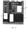
- the electronic component is embedded in the multilayer wiring substrate.
- an electronic component 53 may be embedded in a core substrate 102 which supports a multilayer wiring substrate 101 in which an electronic component 51 is embedded.
Landscapes
- Engineering & Computer Science (AREA)
- Microelectronics & Electronic Packaging (AREA)
- Manufacturing & Machinery (AREA)
- Production Of Multi-Layered Print Wiring Board (AREA)
Abstract
To improve the degree of freedom of design of a multilayer wiring substrate incorporating therein an electronic component. A multilayer wiring substrate 1 includes a first layered structure including conductor layers 13, 14, 15, and 16, and insulation layers 23, 24, 25, and 26 including therein via conductors 33, 34, 35, and 36 each having a diameter which decreases from the upper surface of the insulation layer toward the lower surface thereof; an electronic component 51 embedded in the first layered structure; and a second layered structure stacked on the first layered structure, and including conductor layers 17 and 18, and an insulation layer 27 including therein a via conductor 37 having a diameter which decreases from the upper surface of the insulation layer toward the lower surface thereof.
Description
- The present invention relates to a multilayer wiring substrate having a structure in which a plurality of insulation layers and a plurality of conductor layers are alternately stacked, and to a method for producing the multilayer wiring substrate.
- Hitherto, there has been known a technique for providing a hole in a front-surface portion of a multilayer wiring substrate including a plurality of insulation layers and a plurality of conductor layers, the insulation layers and the conductor layers being alternately stacked, so that the hole penetrates the insulation layers, and accommodating an electronic component in the hole so that the electronic component is incorporated into the multilayer wiring substrate (see, for example, Patent Document 1).
- Patent Document 1: Japanese Patent Application Laid-Open (kokai) No.
2012-99610 - However, in the case of the technique described in
Patent Document 1, a region for incorporation of an electronic component is limited to a portion near the front surface of the wiring substrate, which may reduce the degree of freedom of design of the wiring substrate (e.g., wiring layout in the wiring substrate). - In view of the foregoing, an object of the present invention is to improve the degree of freedom of design of a multilayer wiring substrate incorporating therein an electronic component.
- In order to achieve the aforementioned object, the present invention provides a multilayer wiring substrate comprising a plurality of insulation layers and a plurality of conductor layers, the insulation layers and the conductor layers being alternately stacked, and a via conductor formed in each insulation layer for electrically connecting conductor layers formed on upper and lower surfaces of the insulation layer, the multilayer wiring substrate being characterized by comprising a first layered structure including a plurality of conductor layers, and a plurality of insulation layers each including therein a via conductor having a diameter which decreases from the upper surface of the insulation layer toward the lower surface thereof; an electronic component embedded in the first layered structure; and a second layered structure stacked on the first layered structure, and including at least one conductor layer, and at least one insulation layer including therein a via conductor having a diameter which decreases from the upper surface of the insulation layer toward the lower surface thereof.
- According to the multilayer wiring substrate with this configuration, the electronic component is embedded in the first layered structure, and the second layered structure, which includes at least one insulation layer and at least one conductor layer, is stacked on the first layered structure. Thus, when the number of insulation layers forming the second layered structure is small, the embedded electronic component is located in a region near the upper surface of the multilayer wiring substrate. Meanwhile, when the number of insulation layers forming the second layered structure is large, the embedded electronic component is located in a region away from the upper surface of the multilayer wiring substrate.
- Therefore, according to the multilayer wiring substrate of the present invention, since a region for incorporation of the electronic component is not limited to a portion near the upper surface of the multilayer wiring substrate, the degree of freedom of design can be improved.
- In the multilayer wiring substrate of the present invention, the first layered structure may include a metal layer which is formed below the electronic component so as to be in contact with a lower portion of the electronic component.
- According to the multilayer wiring substrate with this configuration, since heat generated in the electronic component is conducted to the metal layer and released to the outside of the electronic component, the heat release performance of the electronic component can be improved.
- In the multilayer wiring substrate of the present invention, a plurality of electronic components may be embedded in the first layered structure, and the electronic components may be located at different positions on a plane perpendicular to a stacking direction of the first layered structure.
- According to the multilayer wiring substrate with this configuration, the positions of the electronic components embedded in the first layered structure are not limited to a specific one position on a plane perpendicular to the stacking direction of the first layered structure. Therefore, the degree of freedom of the positions of the electronic components incorporated in the multilayer wiring substrate can be improved.
- In the multilayer wiring substrate of the present invention, one electronic component of the electronic components embedded in the first layered structure may be defined as a first electronic component; another electronic component different from the first electronic component may be defined as a second electronic component; among the insulation layers forming the first layered structure, an insulation layer which does not have the first electronic component embedded therein may be defined as a non-embedded insulation layer; and the second electronic component may also be embedded in the non-embedded insulation layer.
- According to the multilayer wiring substrate with this configuration, since a wire can be formed in the non-embedded insulation layer at a region facing the first electronic component in the aforementioned stacking direction, wiring density can be improved in the non-embedded insulation layer.
- In the multilayer wiring substrate of the present invention, the via conductor may be connected to an upper portion of the electronic component, and the via conductor may have a length in the stacking direction of the first layered structure greater than that of the insulation layer through which the via conductor penetrates.
- According to the multilayer wiring substrate with this configuration, when an upper portion of the electronic component is embedded in a first insulation layer, and a second insulation layer is stacked on the first insulation layer, the via conductor penetrates the second insulation layer, extends in the first insulation layer, and is connected to the electronic component. Therefore, the via conductor may be formed through a process in which the second insulation layer is stacked on the first insulation layer, and then a via hole is provided so as to penetrate the second insulation layer, to extend in the first insulation layer, and to reach the electronic component. That is, there is no requirement to carry out a process in which a first via conductor is formed after formation of the first insulation layer, and then a second via conductor is formed after formation of the second insulation layer. Thus, a process of forming the via conductor can be simplified.
- In the multilayer wiring substrate of the present invention, a glass fiber layer may be provided in the first layered structure, and the electronic component may be embedded so as to penetrate the glass fiber layer. Thus, the rigidity of a portion in which the electronic component is embedded (i.e., the first layered structure) can be enhanced in the multilayer wiring substrate.
- In the multilayer wiring substrate of the present invention, the first layered structure may have therein an accommodation hole for accommodating the electronic component in the first layered structure, the accommodation hole being provided before embedment of the electronic component in the first layered structure, and the accommodation hole may have a diameter which decreases downwardly. Thus, the area of the opening of the accommodation hole is larger than that of the bottom thereof. Therefore, the electronic component can be readily accommodated into the accommodation hole through the opening thereof, and the electronic component can be reliably mounted in the multilayer wiring substrate.
- In order to achieve the aforementioned object, the present invention also provides a method for producing a multilayer wiring substrate comprising a plurality of insulation layers and a plurality of conductor layers, the insulation layers and the conductor layers being alternately stacked, and a via conductor formed in each insulation layer for electrically connecting conductor layers formed on upper and lower surfaces of the insulation layer, the method being characterized by comprising a first layered structure formation step of forming a first layered structure including a plurality of conductor layers, and a plurality of insulation layers each including therein a via conductor having a diameter which decreases from the upper surface of the insulation layer toward the lower surface thereof; a metal layer formation step of forming a metal layer in a region in the first layered structure in which an electronic component is to be embedded, the metal layer formation step being carried out during the course of the first layered structure formation step; an accommodation hole provision step of applying a laser beam via an upper surface of the first layered structure toward the metal layer in the first layered structure, to thereby provide an accommodation hole which extends in a stacking direction of the first layered structure to the metal layer, and which does not penetrate the metal layer; an accommodation step of accommodating an electronic component in the accommodation hole; and an insulation layer stacking step of stacking an insulation layer on the first layered structure after accommodation of the electronic component in the accommodation hole.
- This production method is employed for producing the multilayer wiring substrate of the present invention. When this method is carried out, there can be obtained effects similar to those of the multilayer wiring substrate of the present invention.
- The accommodation hole which extends to the metal layer but does not penetrate therethrough is formed through application of a laser beam toward the metal layer in the first layered structure. Therefore, the depth of the accommodation hole can be accurately controlled with respect to the position at which the metal layer is formed.
- Since the electronic component is accommodated in the accommodation hole after provision thereof, the electronic component is embedded so that a lower portion thereof comes into contact with the metal layer. Therefore, heat generated in the electronic component is conducted to the metal layer and released to the outside of the electronic component, and the heat release performance of the electronic component can be improved.
- In the case where heat generated in the electronic component is not required to be released via the metal layer, in the multilayer wiring substrate production method of the present invention, there may be carried out a removal step of removing the metal layer after provision of the accommodation hole and before accommodation of the electronic component in the accommodation hole.
-
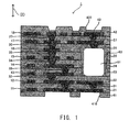
- [
FIG. 1 ]
FIG. 1 is a schematic cross-sectional view of the configuration of amultilayer wiring substrate 1 of a first embodiment. - [
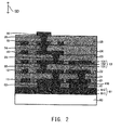
FIG. 2 ]
FIG. 2 shows a process of producing themultilayer wiring substrate 1 of the first embodiment (first cross-sectional view). - [
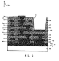
FIG. 3 ]
FIG. 3 shows the process of producing themultilayer wiring substrate 1 of the first embodiment (second cross-sectional view). - [
FIG. 4 ]
FIG. 4 shows the process of producing themultilayer wiring substrate 1 of the first embodiment (third cross-sectional view). - [
FIG. 5 ]
FIG. 5 shows the process of producing themultilayer wiring substrate 1 of the first embodiment (fourth cross-sectional view). - [
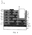
FIG. 6 ]
FIG. 6 shows the process of producing themultilayer wiring substrate 1 of the first embodiment (fifth cross-sectional view). - [
FIG. 7 ]
FIG. 7 shows the process of producing themultilayer wiring substrate 1 of the first embodiment (sixth cross-sectional view). - [
FIG. 8 ]
FIG. 8 shows the process of producing themultilayer wiring substrate 1 of the first embodiment (seventh cross-sectional view). - [
FIG. 9 ]
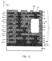
FIG. 9 shows the process of producing themultilayer wiring substrate 1 of the first embodiment (eighth cross-sectional view). - [
FIG. 10 ]
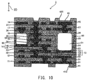
FIG. 10 is a schematic cross-sectional view of the configuration of amultilayer wiring substrate 1 of a second embodiment. - [
FIG. 11 ]
FIG. 11 is a schematic cross-sectional view of the configuration of amultilayer wiring substrate 1 of a third embodiment. - [
FIG. 12 ]
FIG. 12 is a schematic cross-sectional view of the configuration of amultilayer wiring substrate 1 of a fourth embodiment. - [
FIG. 13 ]
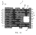
FIG. 13 is a schematic cross-sectional view of the configuration of amultilayer wiring substrate 1 of a fifth embodiment. - [
FIG. 14 ]
FIG. 14 is a schematic cross-sectional view of the configuration of amultilayer wiring substrate 1 of a sixth embodiment. - [
FIG. 15 ]
FIG. 15 is a schematic cross-sectional view of the configuration of a multilayer wiring substrate of another embodiment. - A first embodiment of the present invention will next be described with reference to the drawings.
- As shown in
FIG. 1 , amultilayer wiring substrate 1 of the first embodiment to which the present invention is applied includes a plurality of (eight in the present embodiment) conductor layers 11, 12, 13, 14, 15, 16, 17, and 18, and a plurality of (seven in the present embodiment; i.e., smaller by one in number than the conductor layers 11 to 18) insulation layers 21, 22, 23, 24, 25, 26, and 27, wherein the conductor layers and the insulation layers are alternately stacked in a stacking direction SD. - The insulation layers 21, 22, 23, 24, 25, 26, and 27 forming the
multilayer wiring substrate 1 respectively include therein viaconductors - A solder resist
layer 41 is stacked so as to cover theinsulation layer 21 on the side opposite theinsulation layer 22, and a solder resistlayer 42 is stacked so as to cover theinsulation layer 27 on the side opposite theinsulation layer 26. The solder resistlayers openings Au layer 43 is stacked on theconductor layer 18 exposed through theopenings 420. - An
electronic component 51 is embedded in the insulation layers 23, 24, 25, and 26 forming themultilayer wiring substrate 1. - Next will be described a method for producing the
multilayer wiring substrate 1 to which the present invention is applied. - As shown in
FIG. 2 , firstly, asupport substrate 60 is provided. Thesupport substrate 60 is a plate-like member prepared through, for example, impregnation of glass fiber with an epoxy resin, and exhibits high rigidity. In the production method according to the present embodiment, themultilayer wiring substrate 1 is produced by stacking, on opposite surfaces of thesupport substrate 60, the conductor layers 11 to 18, the insulation layers 21 to 27, and other components. However, in the drawings showing the production method (FIGs. 2 to 9 ), illustration on the lower surface side of thesupport substrate 60 is omitted for the sake of simplification. - A
release sheet 61 is placed, via a prepreg layer (not shown) serving as an adhesive layer, on each of the opposite surfaces of thesupport substrate 60, and therelease sheet 61 is press-bonded to thesupport substrate 60 by means of, for example, a vacuum heating press, to thereby stack therelease sheet 61 on the substrate. Therelease sheet 61 is formed by stacking a metal layer 611 (a copper layer in the present embodiment) and a metal layer 612 (a copper layer in the present embodiment). Since a metal plating layer (e.g., Cr plating layer) is provided between themetal layer 611 and themetal layer 612, themetal layer 611 and themetal layer 612 can be separated from each other. - On each surface side of the
support substrate 60, a film-like resin material (e.g., epoxy resin) is provided on therelease sheet 61, and the resin material is cured through heating under vacuum, to thereby form the solder resistlayer 41. Thus, therelease sheet 61 is covered with the solder resistlayer 41. - Then, on each surface side of the
support substrate 60, a laser beam is applied to specific positions on the surface of the solder resistlayer 41, to thereby provideopenings 410 in the solder resistlayer 41. Subsequently, a desmear treatment is carried out for removing smears generated in the thus-providedopenings 410. Thereafter, electroless plating is carried out, to thereby form a thin electroless plating layer (a copper layer in the present embodiment) on the solder resistlayer 41. Then, a specific resist pattern corresponding to the wiring pattern of theconductor layer 11 is formed on the electroless plating layer. Subsequently, electroplating is carried out, to thereby form a plating layer (a copper layer in the present embodiment) on a region which is not covered with the resist pattern. Thereafter, unwanted electroless plating layer and resist pattern are removed through etching. Thus,metal conductors 62 are formed in theopenings 410, and theconductor layer 11 having a specific wiring pattern is formed. - Then, on each surface side of the
support substrate 60, a film-like resin material (e.g., epoxy resin) is provided on the solder resistlayer 41, and the resin material is cured through heating under vacuum, to thereby form theinsulation layer 21. - Thereafter, a laser beam is applied to specific positions on the surface of the
insulation layer 21, to thereby provide a plurality of via holes in theinsulation layer 21. Subsequently, a desmear treatment is carried out for removing smears generated in the thus-provided via holes. Thereafter, electroless plating is carried out, to thereby form a thin electroless plating layer (a copper layer in the present embodiment) on theinsulation layer 21. Then, a specific resist pattern corresponding to the wiring pattern of theconductor layer 12 is formed on the electroless plating layer. Subsequently, electroplating is carried out, to thereby form a plating layer (a copper layer in the present embodiment) on a region which is not covered with the resist pattern. Thereafter, unwanted electroless plating layer and resist pattern are removed through etching. Thus, the viaconductors 31 are formed in the via holes, and theconductor layer 12 having a specific wiring pattern is formed. - Subsequently, steps similar to those for forming the
insulation layer 21, theconductor layer 12, and the viaconductors 31 are carried out, to thereby form, on theinsulation layer 21, the insulation layers 22, 23, 24, and 25, the conductor layers 13, 14, 15, and 16, and the viaconductors - The
conductor layer 13 is formed of aspecific wiring pattern 131 and adepth controlling pattern 132. The conductor layers 14, 15, and 16 are provided so as not to be located above thedepth controlling pattern 132 in the stacking direction SD. - Thereafter, a laser beam is applied to a specific position on the surface of the
insulation layer 25, the position being located above thedepth controlling pattern 132 in the stacking direction SD, to thereby provide, as shown inFIG. 3 , a bottomedhole 63 which penetrates the insulation layers 25 and 24 and reaches the upper surface of thedepth controlling pattern 132 in theinsulation layer 23. Since the bottomedhole 63 is provided through laser processing, the bottomedhole 63 has a diameter which decreases from the upper surface of theinsulation layer 25 toward thedepth controlling pattern 132. - Then, as shown in
FIG. 4 , a specific resistpattern 64 is formed so as to cover the wiring pattern of theconductor layer 16, followed by etching. Thus, as shown inFIG. 5 , thedepth controlling pattern 132 is removed. - Thereafter, as shown in
FIG. 6 , theelectronic component 51 is accommodated in the bottomedhole 63. Then, theinsulation layer 26 is formed on theinsulation layer 25 in the same manner as employed for formation of the insulation layers 21, 22, 23, 24, and 25. Thus, as shown inFIG. 7 , the upper surface of theinsulation layer 25 and theconductor layer 16 are covered with theinsulation layer 26, and a space between the bottomedhole 63 and theelectronic component 51 is filled with theinsulation layer 26, whereby theelectronic component 51 is embedded in the bottomedhole 63. - Subsequently, a laser beam is applied to specific positions on the surface of the
insulation layer 26, to thereby provide, as shown inFIG. 8 , a plurality of viaholes 65 in theinsulation layer 21. Then, a desmear treatment is carried out for removing smears generated in the via holes 65. Thereafter, electroless plating is carried out, to thereby form a thin electroless plating layer (a copper layer in the present embodiment) on theinsulation layer 26. Then, a specific resist pattern corresponding to the wiring pattern of theconductor layer 17 is formed on the electroless plating layer. Subsequently, electroplating is carried out, to thereby form a plating layer (a copper layer in the present embodiment) on a region which is not covered with the resist pattern. Thereafter, unwanted electroless plating layer and resist pattern are removed through etching. Thus, as shown inFIG. 9 , the viaconductors 36 are formed in the via holes 65, and theconductor layer 17 having a specific wiring pattern is formed. - Subsequently, steps similar to those for forming the
insulation layer 21, theconductor layer 12, and the viaconductors 31 are carried out, to thereby form, on theinsulation layer 26, theinsulation layer 27, theconductor layer 18, and the viaconductors 37. - Then, a solder resist containing an organic resin material (e.g., epoxy resin) is applied so as to cover the
insulation layer 27 and theconductor layer 18, followed by patterning of the solder resist. Thus, there is formed, on theinsulation layer 27, the solder resistlayer 42 having theopenings 420 in regions in which theconductor layer 18 is provided. Subsequently, electroless plating is carried out, to thereby form the Ni/Au layer 43 on theconductor layer 18. - Next, the
metal layer 611 is removed from themetal layer 612, to thereby separate, from thesupport substrate 60, alayered structure 2 including, for example, themetal layer 612, and the conductor layers 11 to 18 and the insulation layers 21 to 27 stacked on themetal layer 612. Thus, twolayered structures 2 are produced. - Thereafter, the
metal layer 612 and themetal conductors 62 are removed through etching, to thereby produce, as shown inFIG. 1 , themultilayer wiring substrate 1, which includes theinsulation layer 21 having thereon the solder resistlayer 41 having theopenings 410 in regions in which theconductor layer 11 is provided. - The
multilayer wiring substrate 1 having the aforementioned configuration includes a first layered structure including the conductor layers 13, 14, 15, and 16, and the insulation layers 23, 24, 25, and 26 including therein the viaconductors electronic component 51 embedded in the first layered structure; and a second layered structure stacked on the first layered structure, and including the conductor layers 17 and 18, and theinsulation layer 27 including therein the viaconductors 37 each having a diameter which decreases from the upper surface of the insulation layer toward the lower surface thereof. - Thus, when the number of insulation layers forming the second layered structure is small, the embedded
electronic component 51 is located in a region near the upper surface of themultilayer wiring substrate 1. Meanwhile, when the number of insulation layers forming the second layered structure is large, the embeddedelectronic component 51 is located in a region away from the upper surface of themultilayer wiring substrate 1. - Therefore, according to the
multilayer wiring substrate 1, since a region for incorporation of theelectronic component 51 is not limited to a portion near the upper surface of themultilayer wiring substrate 1, the degree of freedom of design can be improved. - The method for producing the
multilayer wiring substrate 1 includes a first layered structure formation step of forming a first layered structure including the conductor layers 13, 14, 15, and 16, and the insulation layers 23, 24, 25, and 26 including therein the viaconductors depth controlling pattern 132 in a region in the first layered structure in which theelectronic component 51 is to be embedded, the depth controlling pattern formation step being carried out during the course of the first layered structure formation step; a bottomed hole provision step of applying a laser beam via the upper surface of the first layered structure toward thedepth controlling pattern 132 in the first layered structure, to thereby provide the bottomedhole 63 which extends through the first layered structure in the stacking direction SD to thedepth controlling pattern 132, and which does not penetrate thedepth controlling pattern 132; an accommodation step of accommodating theelectronic component 51 in the bottomedhole 63; and an insulation layer stacking step of stacking theinsulation layer 26 on the first layered structure after accommodation of theelectronic component 51 in the bottomedhole 63. - In the method for producing the
multilayer wiring substrate 1, the bottomedhole 63, which extends to thedepth controlling pattern 132 but does not penetrate therethrough, is formed through application of a laser beam toward thedepth controlling pattern 132 in the first layered structure. Therefore, the depth of the bottomedhole 63 can be accurately controlled with respect to the position at which thedepth controlling pattern 132 is formed. - The bottomed
hole 63 has a diameter which decreases downwardly. Thus, since the area of the opening of the bottomedhole 63 is larger than that of the bottom thereof, theelectronic component 51 can be readily accommodated into the accommodation hole through the opening of the bottomedhole 63, and theelectronic component 51 can be reliably mounted in themultilayer wiring substrate 1. - In the above-described embodiment, the
depth controlling pattern 132 corresponds to the metal layer in the present invention, and the bottomedhole 63 corresponds to the accommodation hole in the present invention. - A second embodiment of the present invention will next be described with reference to the drawings. The following description is focused on the difference between the second embodiment and the first embodiment.
- As shown in
FIG. 10 , themultilayer wiring substrate 1 of the second embodiment has the same configuration as that of the second embodiment, except that anelectronic component 52 is additionally embedded, anddepth controlling patterns 132 and 142 are additionally provided. - The
electronic component 51 is embedded in the insulation layers 23, 24, 25, and 26, whereas theelectronic component 52 is embedded in the insulation layers 24, 25, and 26. - The
depth controlling pattern 132 is formed on theinsulation layer 22. The bottomedhole 63 penetrates theinsulation layer 25 and theinsulation layer 24, and reaches the upper surface of thedepth controlling pattern 132 in theinsulation layer 23. Thus, theelectronic component 51 is embedded in the insulation layers 23, 24, 25, and 26 such that the bottom of theelectronic component 51 is in contact with thedepth controlling pattern 132. - The depth controlling pattern 142 is formed on the
insulation layer 23. A bottomedhole 66 penetrates theinsulation layer 25 and reaches the upper surface of the depth controlling pattern 142 in theinsulation layer 24. Thus, theelectronic component 52 is embedded in the insulation layers 24, 25, and 26 such that the bottom of theelectronic component 52 is in contact with the depth controlling pattern 142. - Next will be described a method for embedding the
electronic components - Firstly, as described in the first embodiment, the insulation layers 22, 23, 24, and 25, the conductor layers 13, 14, 15, and 16, and the via
conductors insulation layer 21. Theconductor layer 13 is formed of thespecific wiring pattern 131 and thedepth controlling pattern 132. Theconductor layer 14 is formed of thespecific wiring pattern 141 and the depth controlling pattern 142. - Thereafter, a laser beam is applied to specific positions on the surface of the
insulation layer 25, the positions being located above thedepth controlling patterns 132 and 142, to thereby provide the bottomedhole 63 which penetrates the insulation layers 25 and 24 and reaches the upper surface of thedepth controlling pattern 132 in theinsulation layer 23, and to provide the bottomedhole 66 which penetrates theinsulation layer 25 and reaches the upper surface of the depth controlling pattern 142 in theinsulation layer 24. - Thereafter, the
electronic component 51 is accommodated in the bottomedhole 63, and theelectronic component 52 is accommodated in the bottomedhole 66. Then, theinsulation layer 26 is formed on theinsulation layer 25. Thus, theelectronic component 51 is embedded in the bottomedhole 63, and theelectronic component 52 is embedded in the bottomedhole 66. - In the
multilayer wiring substrate 1 having the aforementioned configuration, thedepth controlling patterns 132 and 142, which are in contact with the bottoms of theelectronic components electronic components electronic components depth controlling patterns 132 and 142 and released to the outside of theelectronic components electronic components - A third embodiment of the present invention will next be described with reference to the drawings. The following description is focused on the difference between the third embodiment and the second embodiment.
- As shown in
FIG. 11 , themultilayer wiring substrate 1 of the third embodiment has the same configuration as that of the second embodiment, except that thedepth controlling patterns 132 and 142 are omitted. - Specifically, the
electronic component 51 is embedded in the insulation layers 23, 24, 25, and 26 such that the bottom of theelectronic component 51 is in contact with theinsulation layer 22, and theelectronic component 52 is embedded in the insulation layers 24, 25, and 26 such that the bottom of theelectronic component 52 is in contact with theinsulation layer 23. - The
electronic components depth controlling patterns 132 and 142 through etching is additionally carried out after provision of the bottomedholes - In the
multilayer wiring substrate 1 having the aforementioned configuration, theelectronic components multilayer wiring substrate 1, and theelectronic components electronic components multilayered wiring substrate 1 are not limited to a specific one position on a plane perpendicular to the stacking direction SD. Therefore, the degree of freedom of the positions of theelectronic components multilayer wiring substrate 1 can be improved. - A fourth embodiment of the present invention will next be described with reference to the drawings. The following description is focused on the difference between the fourth embodiment and the third embodiment.
- As shown in
FIG. 12 , themultilayer wiring substrate 1 of the fourth embodiment has the same configuration as that of the third embodiment, except that theelectronic component 51 is embedded in the insulation layers 22, 23, 24, and 25. - Next will be described a method for embedding the
electronic components - Firstly, as described in the first embodiment, the insulation layers 21, 22, 23, and 24, the conductor layers 11, 12, 13, 14, and 15, and the via
conductors layer 41. Theconductor layer 12 is formed of aspecific wiring pattern 121 and adepth controlling pattern 122. Theconductor layer 14 is formed of thespecific wiring pattern 141 and the depth controlling pattern 142. - Thereafter, a laser beam is applied to a specific position on the surface of the
insulation layer 25, the position being located above thedepth controlling pattern 122, to thereby provide a bottomedhole 67 which penetrates the insulation layers 24 and 23 and reaches the upper surface of thedepth controlling pattern 122 in theinsulation layer 22. - Then, a specific resist pattern is formed so as to cover the wiring pattern of the
conductor layer 15, followed by etching, to thereby remove thedepth controlling pattern 122. - Thereafter, the
electronic component 51 is accommodated in the bottomedhole 67. Then, theinsulation layer 25 is formed on theinsulation layer 24. Thus, the upper surface of theinsulation layer 24 and theconductor layer 15 are covered with theinsulation layer 25, and a space between the bottomedhole 67 and theelectronic component 51 is filled with theinsulation layer 25, whereby theelectronic component 51 is embedded in the bottomedhole 67. Then, the viaconductors 35 are formed in theinsulation layer 25, and theconductor layer 16 is formed on theinsulation layer 25. - Thereafter, a laser beam is applied to a specific position on the surface of the
insulation layer 25, the position being located above the depth controlling pattern 142, to thereby provide a bottomedhole 66 which penetrates theinsulation layer 25 and reaches the upper surface of the depth controlling pattern 142 in theinsulation layer 24. - Then, a specific resist pattern is formed so as to cover the wiring pattern of the
conductor layer 16, followed by etching, to thereby remove the depth controlling pattern 142. - Thereafter, the
electronic component 52 is accommodated in the bottomedhole 66. Then, theinsulation layer 26 is formed on theinsulation layer 25. Thus, the upper surface of theinsulation layer 25 and theconductor layer 16 are covered with theinsulation layer 26, and a space between the bottomedhole 66 and theelectronic component 52 is filled with theinsulation layer 26, whereby theelectronic component 52 is embedded in the bottomedhole 66. The subsequent steps are carried out in the same manner as described in the first embodiment. - In the
multilayer wiring substrate 1 having the aforementioned configuration, theelectronic component 51 is embedded in the insulation layers 22 and 23 in which theelectronic component 52 is not embedded. Therefore, since a wire can be formed in the insulation layers 22 and 23 (in which theelectronic component 51 is embedded) at a region facing theelectronic component 52 in the stacking direction SD, wiring density can be improved in the insulation layers 22 and 23 in which theelectronic component 51 is embedded. - A fifth embodiment of the present invention will next be described with reference to the drawings. The following description is focused on the difference between the fifth embodiment and the first embodiment.
- As shown in
FIG. 13 , themultilayer wiring substrate 1 of the fifth embodiment has the same configuration as that of the first embodiment, except that the height of theelectronic component 51 is varied, and a viaconductor 68 is provided instead of the viaconductor 36 for connecting theelectronic component 51 to theconductor layer 17. - The height (length in the stacking direction SD) of the
electronic component 51 is smaller than that of the bottomedhole 63. Thus, in the first embodiment, theelectronic component 51 is embedded in the insulation layers 23, 24, 25, and 26, whereas in the fifth embodiment, theelectronic component 51 is embedded in the insulation layers 23, 24, and 25. - The via
conductor 68 electrically connects theelectronic component 51 to theconductor layer 17, and the length of the viaconductor 68 in the stacking direction SD is larger than that of theinsulation layer 26 through which the viaconductor 68 penetrates. - Therefore, the via
conductor 68 is formed through a process in which theinsulation layer 26 is stacked on theinsulation layer 25, and then a via hole is provided so as to penetrate theinsulation layer 26, to extend in theinsulation layer 25, and to reach theelectronic component 51. That is, formation of the viaconductor 68 does not require a process in which the viaconductor 35 is formed after stacking of theinsulation layer 25, and then the viaconductor 36 is formed after stacking of theinsulation layer 26. Thus, the process of forming the viaconductor 68 can be simplified. - A sixth embodiment of the present invention will next be described with reference to the drawings. The following description is focused on the difference between the sixth embodiment and the first embodiment.
- As shown in
FIG. 14 , themultilayer wiring substrate 1 of the sixth embodiment has the same configuration as that of the first embodiment, except that aglass fiber layer 69 is provided in theinsulation layer 24. - Therefore, the bottomed
hole 63 and the viaconductor 34 are provided so as to penetrate theglass fiber layer 69. - In the
multilayer wiring substrate 1 having the aforementioned configuration, theglass fiber layer 69 is provided in theinsulation layer 24, and theelectronic component 51 is embedded so as to penetrate theglass fiber layer 69. Thus, the rigidity of a portion in which theelectronic component 51 is embedded can be enhanced in themultilayer wiring substrate 1. - Although specific embodiments of the present invention have been described above, the present invention is not limited to the embodiments, and various other embodiments may be carried out so long as they fall within the technical scope of the invention.
- In each of the above-described embodiments, the electronic component is embedded in the multilayer wiring substrate. However, for example, as shown in
FIG. 15 , anelectronic component 53 may be embedded in acore substrate 102 which supports amultilayer wiring substrate 101 in which anelectronic component 51 is embedded. -
- 1: multilayer wiring substrate
- 11, 12, 13, 14, 15, 16, 17, 18: conductor layer
- 21, 22, 23, 24, 25, 26, 27: insulation layer
- 31, 32, 33, 34, 35, 36, 37, 68: via conductor
- 51, 52: electronic component
- 63, 66, 67: bottomed hole
- 69: glass fiber layer
- 132, 142: depth controlling pattern
Claims (9)
- A multilayer wiring substrate comprising a plurality of insulation layers and a plurality of conductor layers, the insulation layers and the conductor layers being alternately stacked, and a via conductor formed in each insulation layer for electrically connecting conductor layers formed on upper and lower surfaces of the insulation layer, the multilayer wiring substrate being characterized by comprising:a first layered structure including a plurality of conductor layers, and a plurality of insulation layers each including therein a via conductor having a diameter which decreases from the upper surface of the insulation layer toward the lower surface thereof;an electronic component embedded in the first layered structure; anda second layered structure stacked on the first layered structure, and including at least one conductor layer, and at least one insulation layer including therein a via conductor having a diameter which decreases from the upper surface of the insulation layer toward the lower surface thereof.
- A multilayer wiring substrate according to claim 1, wherein the first layered structure includes a metal layer which is formed below the electronic component so as to be in contact with a lower portion of the electronic component.
- A multilayer wiring substrate according to claim 1 or 2, wherein a plurality of the electronic components are embedded in the first layered structure, and the electronic components are located at different positions on a plane perpendicular to a stacking direction of the first layered structure.
- A multilayer wiring substrate according to claim 3, wherein
one electronic component of the electronic components embedded in the first layered structure is defined as a first electronic component;
another electronic component different from the first electronic component is defined as a second electronic component;
among the insulation layers forming the first layered structure, an insulation layer which does not have the first electronic component embedded therein is defined as a non-embedded insulation layer; and
the second electronic component is also embedded in the non-embedded insulation layer. - A multilayer wiring substrate according to any one of claims 1 to 4, wherein the via conductor to an upper portion of the electronic component has a length in the stacking direction of the first layered structure greater than that of the insulation layer through which the via conductor penetrates.
- A multilayer wiring substrate according to any one of claims 1 to 5, wherein a glass fiber layer is provided in the first layered structure, and the electronic component is embedded so as to penetrate the glass fiber layer.
- A multilayer wiring substrate according to any one of claims 1 to 6, wherein the first layered structure has therein an accommodation hole for accommodating the electronic component in the first layered structure, the accommodation hole being provided before embedment of the electronic component in the first layered structure, and the accommodation hole has a diameter which decreases downwardly.
- A method for producing a multilayer wiring substrate comprising a plurality of insulation layers and a plurality of conductor layers, the insulation layers and the conductor layers being alternately stacked, and a via conductor formed in each insulation layer for electrically connecting conductor layers formed on upper and lower surfaces of the insulation layer, the method being characterized by comprising
a first layered structure formation step of forming a first layered structure including a plurality of conductor layers, and a plurality of insulation layers each including therein a via conductor having a diameter which decreases from the upper surface of the insulation layer toward the lower surface thereof;
a metal layer formation step of forming a metal layer in a region in the first layered structure in which an electronic component is to be embedded, the metal layer formation step being carried out during the course of the first layered structure formation step;
an accommodation hole provision step of applying a laser beam via an upper surface of the first layered structure toward the metal layer in the first layered structure, to thereby provide an accommodation hole which extends in a stacking direction of the first layered structure to the metal layer, and which does not penetrate the metal layer;
an accommodation step of accommodating an electronic component in the accommodation hole; and
an insulation layer stacking step of stacking an insulation layer on the first layered structure after accommodation of the electronic component in the accommodation hole. - A method for producing a multilayer wiring substrate according to claim 8, which comprises a removal step of removing the metal layer after provision of the accommodation hole and before accommodation of the electronic component in the accommodation hole.
Applications Claiming Priority (2)
| Application Number | Priority Date | Filing Date | Title |
|---|---|---|---|
| JP2012271443A JP2014116548A (en) | 2012-12-12 | 2012-12-12 | Multilayer wiring board and manufacturing method therefor |
| PCT/JP2013/005365 WO2014091644A1 (en) | 2012-12-12 | 2013-09-11 | Multilayer wiring substrate and production method therefor |
Publications (1)
| Publication Number | Publication Date |
|---|---|
| EP2934075A1 true EP2934075A1 (en) | 2015-10-21 |
Family
ID=50933958
Family Applications (1)
| Application Number | Title | Priority Date | Filing Date |
|---|---|---|---|
| EP13862412.7A Withdrawn EP2934075A1 (en) | 2012-12-12 | 2013-09-11 | Multilayer wiring substrate and production method therefor |
Country Status (7)
| Country | Link |
|---|---|
| US (1) | US20150327362A1 (en) |
| EP (1) | EP2934075A1 (en) |
| JP (1) | JP2014116548A (en) |
| KR (1) | KR20150084979A (en) |
| CN (1) | CN104854969A (en) |
| TW (1) | TW201431455A (en) |
| WO (1) | WO2014091644A1 (en) |
Families Citing this family (18)
| Publication number | Priority date | Publication date | Assignee | Title |
|---|---|---|---|---|
| KR102281458B1 (en) * | 2014-06-23 | 2021-07-27 | 삼성전기주식회사 | Printed circuit board having an embedded device, semiconductor package and method of manufacturing the same |
| US9704735B2 (en) * | 2014-08-19 | 2017-07-11 | Intel Corporation | Dual side solder resist layers for coreless packages and packages with an embedded interconnect bridge and their methods of fabrication |
| JP6465386B2 (en) | 2014-11-17 | 2019-02-06 | 新光電気工業株式会社 | WIRING BOARD, ELECTRONIC COMPONENT DEVICE, WIRING BOARD MANUFACTURING METHOD, AND ELECTRONIC COMPONENT DEVICE MANUFACTURING METHOD |
| JP6462480B2 (en) * | 2015-04-28 | 2019-01-30 | 新光電気工業株式会社 | Wiring board and method of manufacturing wiring board |
| TWI578416B (en) * | 2015-09-18 | 2017-04-11 | 旭德科技股份有限公司 | Package carrier board and manufacturing method thereof |
| KR20170037331A (en) | 2015-09-25 | 2017-04-04 | 삼성전기주식회사 | Printed circuit board and method for manufacturing the same |
| KR102466206B1 (en) * | 2015-12-16 | 2022-11-11 | 삼성전기주식회사 | Printed circuit board |
| JP7127995B2 (en) * | 2018-03-09 | 2022-08-30 | 日東電工株式会社 | Wiring board manufacturing method |
| JP2020184596A (en) * | 2019-05-09 | 2020-11-12 | イビデン株式会社 | Electronic component built-in wiring board and manufacturing method thereof |
| TWI739182B (en) * | 2019-10-24 | 2021-09-11 | 欣興電子股份有限公司 | Carrier structure and manufacturing method thereof |
| CN112768430B (en) * | 2019-11-06 | 2024-05-14 | 欣兴电子股份有限公司 | Carrier structure and manufacturing method thereof |
| KR102776265B1 (en) * | 2019-12-16 | 2025-03-07 | 삼성전기주식회사 | Substrate with electronic component embedded therein |
| WO2021146894A1 (en) * | 2020-01-21 | 2021-07-29 | 鹏鼎控股(深圳)股份有限公司 | Electronic component-embedded circuit board, and manufacturing method |
| JP7435043B2 (en) * | 2020-03-06 | 2024-02-21 | Tdk株式会社 | Circuit board with built-in electronic components and its manufacturing method |
| CN114793394B (en) * | 2021-01-25 | 2025-05-27 | 礼鼎半导体科技秦皇岛有限公司 | Packaging circuit structure and manufacturing method thereof |
| CN113451259B (en) * | 2021-05-14 | 2023-04-25 | 珠海越亚半导体股份有限公司 | A multi-device sub-embedded packaging substrate and its manufacturing method |
| CN113692112B (en) * | 2021-08-30 | 2023-03-24 | 维沃移动通信有限公司 | Circuit board and manufacturing method thereof |
| KR102946055B1 (en) * | 2021-11-09 | 2026-04-01 | 삼성전기주식회사 | Printed circuit board |
Family Cites Families (10)
| Publication number | Priority date | Publication date | Assignee | Title |
|---|---|---|---|---|
| CN1094717C (en) * | 1995-11-16 | 2002-11-20 | 松下电器产业株式会社 | PC board and fixing body thereof |
| JP4339739B2 (en) * | 2004-04-26 | 2009-10-07 | 太陽誘電株式会社 | Multi-layer board with built-in components |
| JP4252019B2 (en) * | 2004-09-01 | 2009-04-08 | 三洋電機株式会社 | Circuit device and manufacturing method thereof |
| US8101868B2 (en) * | 2005-10-14 | 2012-01-24 | Ibiden Co., Ltd. | Multilayered printed circuit board and method for manufacturing the same |
| JP4673207B2 (en) * | 2005-12-16 | 2011-04-20 | イビデン株式会社 | Multilayer printed wiring board and manufacturing method thereof |
| JP5395360B2 (en) * | 2008-02-25 | 2014-01-22 | 新光電気工業株式会社 | Manufacturing method of electronic component built-in substrate |
| KR101058621B1 (en) * | 2009-07-23 | 2011-08-22 | 삼성전기주식회사 | Semiconductor package and manufacturing method thereof |
| JP2012060056A (en) * | 2010-09-13 | 2012-03-22 | Nec Corp | Electronic apparatus and electronic module |
| JP5655244B2 (en) | 2010-11-01 | 2015-01-21 | 新光電気工業株式会社 | WIRING BOARD AND METHOD FOR MANUFACTURING SAME, SEMICONDUCTOR DEVICE AND METHOD FOR MANUFACTURING SAME |
| US8745860B2 (en) * | 2011-03-11 | 2014-06-10 | Ibiden Co., Ltd. | Method for manufacturing printed wiring board |
-
2012
- 2012-12-12 JP JP2012271443A patent/JP2014116548A/en active Pending
-
2013
- 2013-09-11 CN CN201380065360.3A patent/CN104854969A/en active Pending
- 2013-09-11 KR KR1020157015485A patent/KR20150084979A/en not_active Withdrawn
- 2013-09-11 US US14/651,384 patent/US20150327362A1/en not_active Abandoned
- 2013-09-11 EP EP13862412.7A patent/EP2934075A1/en not_active Withdrawn
- 2013-09-11 WO PCT/JP2013/005365 patent/WO2014091644A1/en not_active Ceased
- 2013-12-02 TW TW102143955A patent/TW201431455A/en unknown
Non-Patent Citations (1)
| Title |
|---|
| See references of WO2014091644A1 * |
Also Published As
| Publication number | Publication date |
|---|---|
| WO2014091644A1 (en) | 2014-06-19 |
| US20150327362A1 (en) | 2015-11-12 |
| KR20150084979A (en) | 2015-07-22 |
| JP2014116548A (en) | 2014-06-26 |
| TW201431455A (en) | 2014-08-01 |
| CN104854969A (en) | 2015-08-19 |
Similar Documents
| Publication | Publication Date | Title |
|---|---|---|
| US20150327362A1 (en) | Multilayer wiring substrate and production method therefor | |
| KR101884430B1 (en) | Multi-layer type printed circuit board and Method of manufacturing the same | |
| CN103796451B (en) | Printed wiring board and the manufacture method of printed wiring board | |
| US9179553B2 (en) | Method of manufacturing multilayer wiring board | |
| WO2014091869A1 (en) | Wiring substrate and production method therefor | |
| US20140027156A1 (en) | Multilayer type coreless substrate and method of manufacturing the same | |
| KR102268388B1 (en) | Printed circuit board and manufacturing method thereof | |
| JP2012094662A (en) | Method of manufacturing multilayer wiring board | |
| KR20140086824A (en) | Method of manufacturing wiring substrate | |
| US20130220691A1 (en) | Multilayer wiring substrate and method of manufacturing the same | |
| KR20180036871A (en) | method of fabricating printed circuit board including solder resist patterns with uniform thickness | |
| KR20120040892A (en) | The printed circuit board and the method for manufacturing the same | |
| US9078344B2 (en) | Printed circuit board and manufacturing method thereof | |
| KR101154605B1 (en) | The printed circuit board and the method for manufacturing the same | |
| US8497434B2 (en) | Printed circuit board and manufacturing method thereof | |
| JP5608262B2 (en) | Printed circuit board and printed circuit board manufacturing method | |
| US20120312591A1 (en) | Printed Circuit Board and Method of Manufacturing the Same | |
| JP2014192223A (en) | Method for manufacturing wiring board | |
| JP4227967B2 (en) | Substrate and electronic component manufacturing method | |
| JP2014138093A (en) | Wiring board | |
| US20130146337A1 (en) | Multi-layered printed circuit board and manufacturing method thereof | |
| JP2014116500A (en) | Method for manufacturing wiring board | |
| JP2012160558A (en) | Method for manufacturing wiring board | |
| KR20160034168A (en) | Printed circuit board and manufacturing method thereof | |
| KR101514485B1 (en) | Carrier for manufacturing printed circuit board and method for manufacturing printed circuit board using the same |
Legal Events
| Date | Code | Title | Description |
|---|---|---|---|
| PUAI | Public reference made under article 153(3) epc to a published international application that has entered the european phase |
Free format text: ORIGINAL CODE: 0009012 |
|
| 17P | Request for examination filed |
Effective date: 20150612 |
|
| AK | Designated contracting states |
Kind code of ref document: A1 Designated state(s): AL AT BE BG CH CY CZ DE DK EE ES FI FR GB GR HR HU IE IS IT LI LT LU LV MC MK MT NL NO PL PT RO RS SE SI SK SM TR |
|
| AX | Request for extension of the european patent |
Extension state: BA ME |
|
| DAX | Request for extension of the european patent (deleted) | ||
| STAA | Information on the status of an ep patent application or granted ep patent |
Free format text: STATUS: THE APPLICATION HAS BEEN WITHDRAWN |
|
| 18W | Application withdrawn |
Effective date: 20160516 |