EP2933343A1 - Grain-oriented electrical steel sheet and method for manufacturing the same - Google Patents
Grain-oriented electrical steel sheet and method for manufacturing the same Download PDFInfo
- Publication number
- EP2933343A1 EP2933343A1 EP13851438.5A EP13851438A EP2933343A1 EP 2933343 A1 EP2933343 A1 EP 2933343A1 EP 13851438 A EP13851438 A EP 13851438A EP 2933343 A1 EP2933343 A1 EP 2933343A1
- Authority
- EP
- European Patent Office
- Prior art keywords
- closure domain
- steel sheet
- depth
- closure
- sheet thickness
- Prior art date
- Legal status (The legal status is an assumption and is not a legal conclusion. Google has not performed a legal analysis and makes no representation as to the accuracy of the status listed.)
- Granted
Links
Images




Classifications
-
- H—ELECTRICITY
- H01—ELECTRIC ELEMENTS
- H01F—MAGNETS; INDUCTANCES; TRANSFORMERS; SELECTION OF MATERIALS FOR THEIR MAGNETIC PROPERTIES
- H01F1/00—Magnets or magnetic bodies characterised by the magnetic materials therefor; Selection of materials for their magnetic properties
- H01F1/01—Magnets or magnetic bodies characterised by the magnetic materials therefor; Selection of materials for their magnetic properties of inorganic materials
- H01F1/03—Magnets or magnetic bodies characterised by the magnetic materials therefor; Selection of materials for their magnetic properties of inorganic materials characterised by their coercivity
- H01F1/12—Magnets or magnetic bodies characterised by the magnetic materials therefor; Selection of materials for their magnetic properties of inorganic materials characterised by their coercivity of soft-magnetic materials
- H01F1/14—Magnets or magnetic bodies characterised by the magnetic materials therefor; Selection of materials for their magnetic properties of inorganic materials characterised by their coercivity of soft-magnetic materials metals or alloys
- H01F1/147—Alloys characterised by their composition
- H01F1/14766—Fe-Si based alloys
- H01F1/14775—Fe-Si based alloys in the form of sheets
-
- C—CHEMISTRY; METALLURGY
- C21—METALLURGY OF IRON
- C21D—MODIFYING THE PHYSICAL STRUCTURE OF FERROUS METALS; GENERAL DEVICES FOR HEAT TREATMENT OF FERROUS OR NON-FERROUS METALS OR ALLOYS; MAKING METAL MALLEABLE, e.g. BY DECARBURISATION OR TEMPERING
- C21D1/00—General methods or devices for heat treatment, e.g. annealing, hardening, quenching or tempering
- C21D1/34—Methods of heating
- C21D1/38—Heating by cathodic discharges
-
- C—CHEMISTRY; METALLURGY
- C21—METALLURGY OF IRON
- C21D—MODIFYING THE PHYSICAL STRUCTURE OF FERROUS METALS; GENERAL DEVICES FOR HEAT TREATMENT OF FERROUS OR NON-FERROUS METALS OR ALLOYS; MAKING METAL MALLEABLE, e.g. BY DECARBURISATION OR TEMPERING
- C21D1/00—General methods or devices for heat treatment, e.g. annealing, hardening, quenching or tempering
- C21D1/34—Methods of heating
-
- C—CHEMISTRY; METALLURGY
- C21—METALLURGY OF IRON
- C21D—MODIFYING THE PHYSICAL STRUCTURE OF FERROUS METALS; GENERAL DEVICES FOR HEAT TREATMENT OF FERROUS OR NON-FERROUS METALS OR ALLOYS; MAKING METAL MALLEABLE, e.g. BY DECARBURISATION OR TEMPERING
- C21D6/00—Heat treatment of ferrous alloys
- C21D6/008—Heat treatment of ferrous alloys containing Si
-
- C—CHEMISTRY; METALLURGY
- C21—METALLURGY OF IRON
- C21D—MODIFYING THE PHYSICAL STRUCTURE OF FERROUS METALS; GENERAL DEVICES FOR HEAT TREATMENT OF FERROUS OR NON-FERROUS METALS OR ALLOYS; MAKING METAL MALLEABLE, e.g. BY DECARBURISATION OR TEMPERING
- C21D8/00—Modifying the physical properties of ferrous metals or ferrous alloys by deformation combined with, or followed by, heat treatment
- C21D8/12—Modifying the physical properties of ferrous metals or ferrous alloys by deformation combined with, or followed by, heat treatment during manufacturing of articles with special electromagnetic properties
-
- C—CHEMISTRY; METALLURGY
- C21—METALLURGY OF IRON
- C21D—MODIFYING THE PHYSICAL STRUCTURE OF FERROUS METALS; GENERAL DEVICES FOR HEAT TREATMENT OF FERROUS OR NON-FERROUS METALS OR ALLOYS; MAKING METAL MALLEABLE, e.g. BY DECARBURISATION OR TEMPERING
- C21D8/00—Modifying the physical properties of ferrous metals or ferrous alloys by deformation combined with, or followed by, heat treatment
- C21D8/12—Modifying the physical properties of ferrous metals or ferrous alloys by deformation combined with, or followed by, heat treatment during manufacturing of articles with special electromagnetic properties
- C21D8/1244—Modifying the physical properties of ferrous metals or ferrous alloys by deformation combined with, or followed by, heat treatment during manufacturing of articles with special electromagnetic properties characterised by the heat treatment
-
- C—CHEMISTRY; METALLURGY
- C21—METALLURGY OF IRON
- C21D—MODIFYING THE PHYSICAL STRUCTURE OF FERROUS METALS; GENERAL DEVICES FOR HEAT TREATMENT OF FERROUS OR NON-FERROUS METALS OR ALLOYS; MAKING METAL MALLEABLE, e.g. BY DECARBURISATION OR TEMPERING
- C21D9/00—Heat treatment, e.g. annealing, hardening, quenching or tempering, adapted for particular articles; Furnaces therefor
- C21D9/46—Heat treatment, e.g. annealing, hardening, quenching or tempering, adapted for particular articles; Furnaces therefor for sheet metals
-
- C—CHEMISTRY; METALLURGY
- C22—METALLURGY; FERROUS OR NON-FERROUS ALLOYS; TREATMENT OF ALLOYS OR NON-FERROUS METALS
- C22C—ALLOYS
- C22C38/00—Ferrous alloys, e.g. steel alloys
- C22C38/02—Ferrous alloys, e.g. steel alloys containing silicon
-
- H—ELECTRICITY
- H01—ELECTRIC ELEMENTS
- H01F—MAGNETS; INDUCTANCES; TRANSFORMERS; SELECTION OF MATERIALS FOR THEIR MAGNETIC PROPERTIES
- H01F1/00—Magnets or magnetic bodies characterised by the magnetic materials therefor; Selection of materials for their magnetic properties
- H01F1/01—Magnets or magnetic bodies characterised by the magnetic materials therefor; Selection of materials for their magnetic properties of inorganic materials
- H01F1/03—Magnets or magnetic bodies characterised by the magnetic materials therefor; Selection of materials for their magnetic properties of inorganic materials characterised by their coercivity
- H01F1/12—Magnets or magnetic bodies characterised by the magnetic materials therefor; Selection of materials for their magnetic properties of inorganic materials characterised by their coercivity of soft-magnetic materials
- H01F1/14—Magnets or magnetic bodies characterised by the magnetic materials therefor; Selection of materials for their magnetic properties of inorganic materials characterised by their coercivity of soft-magnetic materials metals or alloys
- H01F1/16—Magnets or magnetic bodies characterised by the magnetic materials therefor; Selection of materials for their magnetic properties of inorganic materials characterised by their coercivity of soft-magnetic materials metals or alloys in the form of sheets
-
- H—ELECTRICITY
- H01—ELECTRIC ELEMENTS
- H01F—MAGNETS; INDUCTANCES; TRANSFORMERS; SELECTION OF MATERIALS FOR THEIR MAGNETIC PROPERTIES
- H01F41/00—Apparatus or processes specially adapted for manufacturing or assembling magnets, inductances or transformers; Apparatus or processes specially adapted for manufacturing materials characterised by their magnetic properties
-
- C—CHEMISTRY; METALLURGY
- C21—METALLURGY OF IRON
- C21D—MODIFYING THE PHYSICAL STRUCTURE OF FERROUS METALS; GENERAL DEVICES FOR HEAT TREATMENT OF FERROUS OR NON-FERROUS METALS OR ALLOYS; MAKING METAL MALLEABLE, e.g. BY DECARBURISATION OR TEMPERING
- C21D1/00—General methods or devices for heat treatment, e.g. annealing, hardening, quenching or tempering
- C21D1/06—Surface hardening
- C21D1/09—Surface hardening by direct application of electrical or wave energy; by particle radiation
-
- C—CHEMISTRY; METALLURGY
- C21—METALLURGY OF IRON
- C21D—MODIFYING THE PHYSICAL STRUCTURE OF FERROUS METALS; GENERAL DEVICES FOR HEAT TREATMENT OF FERROUS OR NON-FERROUS METALS OR ALLOYS; MAKING METAL MALLEABLE, e.g. BY DECARBURISATION OR TEMPERING
- C21D2201/00—Treatment for obtaining particular effects
- C21D2201/05—Grain orientation
Definitions
- the present invention relates to a grain-oriented electrical steel sheet for use in an iron core of a transformer or the like and to a method for manufacturing the grain-oriented electrical steel sheet.
- the loss occurring in a transformer is mainly composed of copper loss occurring in conducting wires and iron loss occurring in the iron core.
- Iron loss can be further divided into hysteresis loss and eddy current loss. To reduce the former, measures such as improving the crystal orientation of the material and reducing impurities have proven effective.
- JP 2012-1741 A discloses a method for manufacturing a grain-oriented electrical steel sheet with excellent flux density and iron loss properties by optimizing the annealing conditions before final cold rolling.
- the eddy current loss is also known to improve dramatically by the formation of a groove or the introduction of strain on the surface of the steel sheet.
- JP H06-22179 B2 discloses a technique for forming a linear groove, with a groove width of 300 ⁇ m or less and a groove depth of 100 ⁇ m or less, on one surface of a steel sheet so as to reduce the iron loss W 17/50 , which was 0.80 W/kg or more before groove formation, to 0.70 W/kg or less.
- JP 2011-246782 A discloses a technique for irradiating a secondary recrystallized steel sheet with a plasma arc so as to reduce the iron loss W 17/50 , which was 0.80 W/kg or more before irradiation, to 0.65 W/kg or less.
- JP 2012-52230 A discloses a technique for obtaining material for a transformer with low iron loss and little noise by optimizing the coating thickness and the average width of a magnetic domain discontinuous portion formed on the surface of a steel sheet by electron beam irradiation.
- JP 2000-328139 A (PTL 5) and JP 4705382 B2 (PTL 6) disclose techniques for improving the effect of reducing iron loss of a grain-oriented electrical steel sheet from thick sheet material by optimizing the laser irradiation conditions in accordance with the sheet thickness of the material.
- PTL 6 discloses having obtained extremely low iron loss by setting the strain ratio ⁇ to 0.00013 or more and 0.013 or less.
- This strain ratio ⁇ is the ratio of the strain area within a rolling direction cross-section of the steel sheet and is expressed by the formula ⁇ /8 ⁇ (w ⁇ w)/(t ⁇ PL), where t is the thickness of the steel sheet, w is the closure domain width in the rolling direction, and PL is the laser irradiation spacing in the rolling direction.
- NPL 1 IEEE TRANSACTIONS ON MAGNETICS, VOL. MAG-20, NO. 5, p.1557
- FIG. 1 illustrates the effect of the strain ratio ⁇ on the iron loss after electron beam irradiation of a sheet with a sheet thickness of 0.27 mm.
- FIG. 1 shows that iron loss of a steel sheet can be reduced, for example to W 17/50 ⁇ 0.76 W/kg, regardless of whether the strain ratio is 0.013 or more or is 0.013 or less.
- the strain ratio is in a range of 0.013 or less and 0.00013 or more as well, the iron loss is sometimes a high value of 0.78 W/kg or more, clearly showing that low iron loss is not always obtained.
- FIG. 2 illustrates the relationship between the width w and depth h of the closure domain occurring in the portions irradiated by the laser and electron beam. It was observed that when using a laser, as the width increases, the depth tends to increase at a degree of accuracy such that the correlation coefficient R 2 is approximately 0.45, whereas when using an electron beam, the correlation coefficient between width and depth was low, and no clear correlation could be observed.
- the present invention has been conceived in light of the above circumstances and proposes a grain-oriented electrical steel sheet, and method for manufacturing the same, with reduced iron loss over a wide range of sheet thickness by forming a closure domain shape advantageous for iron loss reduction that utilizes electron beam characteristics and forming a closure domain that is appropriate for the sheet thickness.
- the inventors conceived of separately controlling the width and the depth of the portion where the closure domain is formed in the portion irradiated during electron beam irradiation.
- the reason is that, for example in JP H11-279645 A (PTL 7), an increase in the depth in the sheet thickness direction has been shown to be advantageous for reducing the eddy current loss of material.
- JP 4344264 B2 shows that since strain is accumulated in the portion where the closure domain is formed, shrinking the portion where the closure domain is formed is useful for suppressing deterioration of hysteresis loss.
- the inventors realized that, as illustrated in FIG. 3 , hysteresis loss worsens more when the sheet thickness is large, even for beam irradiation with the same conditions for irradiation energy and the like.
- a thick sheet material should preferably be irradiated under conditions such that hysteresis loss does not worsen while maintaining the same depth of the portion where the closure domain is formed as in a thin sheet material, i.e. such that the portion where the closure domain is formed is made thinner.
- FIG. 4 illustrates the effect of the depth of the portion where the closure domain is formed on the rate of improvement in eddy current loss with respect to the eddy current loss when the depth of the portion where the closure domain is formed is 45 ⁇ m.
- FIG. 5 illustrates the effect of a volume index for the portion where the closure domain is formed (width ⁇ depth of the portion where the closure domain is formed/RD line spacing) on the rate of improvement in hysteresis loss with respect to the hysteresis loss when the volume index for the portion where the closure domain is formed is 1.1 ⁇ m.
- FIGS. 4 and 5 show how the eddy current loss tends to improve for a larger depth of the portion where the closure domain is formed and how the hysteresis loss tends to worsen for a larger volume of the portion where the closure domain is formed.
- FIG. 6 illustrates the depth of the portion where the closure domain is formed that is necessary to set the rate of improvement in eddy current loss, calculated based on the above results, to 3 % or 5 % (a more preferable condition).
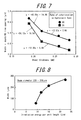
- FIG. 7 illustrates the volume index for the portion where the closure domain is formed that is necessary to set the rate of deterioration of hysteresis loss to 5 % or 3 % (a more preferable condition).
- FIGS. 6 and 7 clearly show that the steel sheet thickness, depth, and width ⁇ depth/RD line spacing (volume index for the portion where the closure domain is formed) have a preferable relationship in a portion where the closure domain is formed that is advantageous for reducing iron loss.
- the inventors identified that for a constant average beam scanning rate, the width of the portion where the closure domain is formed increases as the irradiation energy per unit scanning length of the beam and the beam diameter increase (where P > 45 (J/m/mm)) and that the depth of the portion where the closure domain is formed is affected by the "irradiation energy per unit length/beam diameter" of the beam and by the acceleration voltage.
- FIG. 8 illustrates the effect of irradiation energy per unit scanning length on the width of the portion where the closure domain is formed.
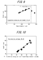
- FIG. 9 illustrates the effect of the beam diameter on the width of the portion where the closure domain is formed.
- FIG. 10 illustrates the effect of P (irradiation energy per unit scanning length/beam diameter) on the depth of the portion where the closure domain is formed.
- FIG. 11 illustrates the effect of the acceleration voltage on the depth of the portion where the closure domain is formed.
- the present invention is based on the above-described findings.
- a closure domain shape advantageous for iron loss reduction that utilizes electron beam characteristics can be formed, and by forming a closure domain that is appropriate for the sheet thickness, iron loss can be reduced in a grain-oriented electrical steel sheet over a wide range of sheet thickness. Accordingly, the present invention allows for an increase in energy usage efficiency of a transformer produced with a grain-oriented electrical steel sheet of any sheet thickness and is therefore industrially useful.
- the present invention provides a grain-oriented electrical steel sheet, and a preferable method for manufacturing the grain-oriented electrical steel sheet, that has a magnetic domain refined by irradiation with an electron beam.
- An insulating coating may be formed on the electrical steel sheet irradiated with an electron beam, yet omitting the insulating coating poses no problem.
- a linearly extending closure domain that segments the main magnetic domain is formed in the portion irradiated by the electron beam.
- the thickness of the grain-oriented electrical steel sheet used in the present invention is preferably, in industrial terms, approximately 0.1 mm to 0.35 mm.
- the present invention may be applied to any conventionally known grain-oriented electrical steel sheet, for example regardless of whether inhibitor components are included.
- the grain-oriented electrical steel sheet of the present invention has a linearly extending closure domain shape, as described below. Note that simply referring to a closure domain below designates a region with a linearly extending closure domain shape. Also note that a unit adjustment term has been included in the coefficient for the letters into which numerical values are substituted in the equations below. Therefore, the numerical values may be substituted as non-dimensional values, ignoring units.
- the volume of the portion where the closure domain is formed is represented as a volume index for the portion where the closure domain is formed that is necessary to set the rate of hysteresis deterioration (absolute value of rate of improvement) to 5 % or 3 % as follows: w ⁇ h / s ⁇ 1000 ⁇ - 12.6 ⁇ t + 7.9 t > 0.22 , and w ⁇ h / s ⁇ 1000 ⁇ - 40.6 ⁇ t + 14.1 t ⁇ 0.22 , and more preferably w ⁇ h / s ⁇ 1000 ⁇ - 12.3 ⁇ t + 6.9 t > 0.22 , and w ⁇ h / s ⁇ 1000 ⁇ - 56.1 ⁇ t + 16.5 t ⁇ 0.22 , where h ( ⁇ m) is the depth of the closure domain, w ( ⁇ m) is the width of the closure domain, s (mm) is the RD line spacing
- the portion where the closure domain is formed is not preferable from the perspective of reducing hysteresis loss, and the volume thereof is preferably small.
- the volume of the portion where the closure domain is formed is proportional to the value yielded by dividing the area of the closure domain shape in a rolling direction cross-section parallel to the sheet thickness direction, obtained by observing a sheet thickness cross-section in the rolling direction (i.e. the area of the cross-sectional shape), by the spacing of the closure domain formed periodically in the rolling direction (RD line spacing: s). Therefore, in the present invention, this area of the cross-sectional shape/RD line spacing is used as a volume index.
- the average area is preferably used.
- variation in the area of the cross-sectional shape is large, it is possible to make measurement of only the closure domain shape observed in a sheet thickness cross-section in the rolling direction for a characteristic portion.
- the closure domain shape in a dot-centered portion may differ from the closure domain shape between dots, yet in this case, the average of the widths and depths yielded by observing cross-sections are preferably used.
- the depth h of the portion where the closure domain is formed is important for the depth h of the portion where the closure domain is formed to satisfy the following relationships (rate of improvement in eddy current loss: 3 %) with the actually measured thickness t (mm) of the steel sheet: h ⁇ 74.9 ⁇ t + 39.1 0.26 ⁇ t , and h ⁇ 897 ⁇ t - 174.7 t > 0.26 and more preferably the following relationships (rate of improvement in eddy current loss: 5 %): h ⁇ 168 ⁇ t + 29.0 0.26 ⁇ t , and h ⁇ 1890 ⁇ t - 418.7 t > 0.26 .
- the shape of the cross-sectional closure domain can be measured with a Kerr effect microscope.
- the (100) face of the crystal is set as the observation face. The reason is that if the observation face is misaligned from the (100) face, a different domain structure is more easily expressed due to a surface magnetic pole occurring on the observation face, making it more difficult to observe the desired closure domain.
- FIG. 13 is a schematic representation of an observational image under a Kerr effect microscope.
- the region of the closure domain shape corresponds to the region of induced strain
- a minute strain distribution in which a closure domain is formed may be observed by x-ray or electron beam and quantified.
- the sheet thickness is included as a parameter for the appropriate closure domain volume.
- the closure domain As the depth of the closure domain in the sheet thickness direction is larger, the closure domain is more advantageous for improving eddy current loss. For a large sheet thickness, however, domain refinement is difficult, perhaps because the domain wall energy is large. Accordingly, in order to obtain a sufficient magnetic domain refining effect, it is necessary to form a deeper closure domain.
- the penetration depth of the electrons in the steel increases, which is advantageous for a deeper closure domain shape. Furthermore, high acceleration voltage is preferable for obtaining a high magnetic domain refining effect in thick sheet material.
- the depth of the portion where the closure domain is formed also depends, however, on the irradiation energy per unit scanning length/beam diameter (P). When P is large, a narrow region is irradiated with extremely high-density energy. Hence, the electrons penetrate more easily in the sheet thickness direction. For this reason, when P is large, the lower limit on the acceleration voltage decreases.
- P is excessively small, i.e. when the irradiation energy is low to begin with, or when the irradiation energy density is low since both the irradiation energy and the beam diameter are large, then the steel sheet cannot be provided with strain, and the effect of reducing iron loss is lessened. Therefore, in the present invention, P is set to exceed 45. While there is no restriction on the upper limit of P, an excessively large P significantly damages the coating and makes it impossible to ensure an anti-corrosion property. Therefore, the upper limit preferably is approximately 300.
- the steel sheet is irradiated with the electron beam linearly from one edge in the width direction to the other edge, and the irradiation is repeated periodically in the rolling direction.
- the spacing (line spacing) s is preferably 3 mm to 12 mm. The reason is that if the line spacing is narrow, the strain region formed in the steel becomes excessively large, and iron loss (hysteresis loss) worsens. On the other hand, if the line spacing is too wide, the magnetic domain refining effect lessens no matter how much the closure domain extends in the depth direction, and iron loss does not improve. Accordingly, in the present invention, the RD line spacing s is set in a range of 3 mm to 12 mm.
- the direction from the starting point to the ending point is set to be from 60° to 120° with respect to the rolling direction.
- linear refers not only to a straight line, but also to a dotted line or a discontinuous line
- the line angle refers to the angle between the rolling direction and a straight line connecting the starting point with the ending point.
- the length of the portion not irradiated with the beam between dots along the line or between continuous line segments is preferably 0.8 mm or less. The reason is that if irradiated region is excessively small, the effect of improving the eddy current loss may be lessened.
- the processing chamber pressure is set to 3 Pa or less. In terms of practical operation, the lower limit on the processing chamber pressure is approximately 0.001 Pa.
- the closure domain width and the beam diameter are correlated, and as the beam diameter is smaller, the closure domain width tends to decrease. Accordingly, a small (narrow) beam diameter is good, with a beam diameter of 400 ⁇ m or less being preferable. If the beam diameter is too small, however, the steel substrate and coating at the irradiated portion are damaged, dramatically decreasing the insulation properties of the steel sheet. Furthermore, in order to significantly reduce the beam diameter, the WD (distance from the focusing coil to the steel sheet) must be shortened, yet doing so causes the beam diameter to vary excessively in the deflection direction (sheet transverse direction) of the beam. The quality of the steel sheet thus easily becomes uneven in the width direction. Accordingly, the beam diameter is preferably 150 ⁇ m or more.
- LaB 6 cathode In general, a LaB 6 cathode is known to be advantageous for outputting a high-intensity beam, and since the beam diameter is easily focused, LaB 6 is preferably used as the emission source for the electron beam in the present invention.
- the focusing conditions are of course preferably adjusted in advance so that the beam is uniform in the width direction.
- Table 1 No. Sheet thickness (mm) Beam cathode material Acceleration voltage (kV) Line spacing (mm) Beam diameter ( ⁇ m) Irradiation energy per unit length (J/m) P (J/m/mm) Closure domain width ( ⁇ m) Closure domain depth ( ⁇ m) 1 0.26 LaB 6 60 4.0 320 17 53 250 50 2 0.26 LaB 6 150 3.5 320 18 55 255 65 3 0.26 LaB 6 150 6.0 320 21 66 270 70 4 0.26 LaB 6 150 3.5 350 15 43 230 55 5 0.26 LaB 6 60 5.0 350 23 66 275 65 6 0.26 LaB 6 60 6.0 320 24 75 280 75 7 0.285 LaB 6 70 5.0 240 16 68 230 65 8 0.285 LaB 6 150 6.0 350 19 54 270 65 9 0.285 LaB 6 150 5.0 260 19 73 250 85 10 0.285 LaB 6 70 4.0 310 20 64 270 65 11 0.285 LaB 6 60 6.0 230 20 87
- the closure domain shape of these steel sheets, No. 1 to 18, was evaluated according to the assessments below, and the iron loss W 17/50 was measured.
- the measurement results and the like are shown in Table 2. Note that the depth and the width of the closure domain are respectively h ( ⁇ m) and w ( ⁇ m), and the RD line spacing is s (mm).
- the iron loss is the average of measurements for 15 sheets under each set of conditions.
- Table 2 shows that applying the present technique yields a grain-oriented electrical steel sheet with low iron loss, such that W 17/50 is 0.68 W/kg or less (t: 0.19 mm), 0.74 W/kg or less (t: 0.26 mm), or 0.85 W/kg or less (t: 0.285 mm).
Landscapes
- Chemical & Material Sciences (AREA)
- Engineering & Computer Science (AREA)
- Physics & Mathematics (AREA)
- Mechanical Engineering (AREA)
- Organic Chemistry (AREA)
- Metallurgy (AREA)
- Materials Engineering (AREA)
- Thermal Sciences (AREA)
- Crystallography & Structural Chemistry (AREA)
- Power Engineering (AREA)
- Manufacturing & Machinery (AREA)
- Electromagnetism (AREA)
- Dispersion Chemistry (AREA)
- Manufacturing Of Steel Electrode Plates (AREA)
- Soft Magnetic Materials (AREA)
- Optics & Photonics (AREA)
- Welding Or Cutting Using Electron Beams (AREA)
Abstract
Description
- The present invention relates to a grain-oriented electrical steel sheet for use in an iron core of a transformer or the like and to a method for manufacturing the grain-oriented electrical steel sheet.
- In recent years, energy use has become more efficient, and demand has emerged for a reduction in energy loss at the time of operation, for example in a transformer.
- The loss occurring in a transformer is mainly composed of copper loss occurring in conducting wires and iron loss occurring in the iron core.
- Iron loss can be further divided into hysteresis loss and eddy current loss. To reduce the former, measures such as improving the crystal orientation of the material and reducing impurities have proven effective. For example,
JP 2012-1741 A - On the other hand, in addition to reducing sheet thickness and increasing the added amount of Si, the eddy current loss is also known to improve dramatically by the formation of a groove or the introduction of strain on the surface of the steel sheet.
- For example,
JP H06-22179 B2 -
JP 2011-246782 A - Furthermore,
JP 2012-52230 A - It is known, however, that the iron loss reduction effect achieved by such groove formation or introduction of strain differs depending on the sheet thickness of the material. For example, IEEE TRANSACTIONS ON MAGNETICS, VOL. MAG-20, NO. 5, p.1557 (NPL 1) describes how, as the sheet thickness increases, the amount of reduction in iron loss due to laser irradiation tends to decrease and notes a difference of approximately 0.05 W/kg in the amount of reduction in iron loss (ΔW17/50) between sheet thicknesses of 0.23 mm and 0.30 mm for a material with a flux density of 1.94 T.
- Against this background, studies have been made of whether the effect of reducing iron loss of thick sheet material can be improved even slightly by adjusting the magnetic domain refining method. For example,
JP 2000-328139 A JP 4705382 B2 PTL 6 discloses having obtained extremely low iron loss by setting the strain ratio η to 0.00013 or more and 0.013 or less. - This strain ratio η is the ratio of the strain area within a rolling direction cross-section of the steel sheet and is expressed by the formula π/8 × (w × w)/(t × PL), where t is the thickness of the steel sheet, w is the closure domain width in the rolling direction, and PL is the laser irradiation spacing in the rolling direction.
- Patent Literature
- PTL 1:
JP 2012-1741 A - PTL 2:
JP H06-22179 B2 - PTL 3:
JP 2011-246782 A - PTL 4:
JP 2012-52230 A - PTL 5:
JP 2000-328139 A - PTL 6:
JP 4705382 B2 - PTL 7:
JP H11-279645 A - PTL 8:
JP 4344264 B2 - NPL 1: IEEE TRANSACTIONS ON MAGNETICS, VOL. MAG-20, NO. 5, p.1557
- The inventors of the present invention conjectured that such a technique used in a laser method could also be applied to an electron beam method and therefore investigated the relationship between the strain ratio and iron loss in order to reduce the iron loss of a steel sheet.
FIG. 1 illustrates the effect of the strain ratio η on the iron loss after electron beam irradiation of a sheet with a sheet thickness of 0.27 mm.FIG. 1 shows that iron loss of a steel sheet can be reduced, for example to W17/50 < 0.76 W/kg, regardless of whether the strain ratio is 0.013 or more or is 0.013 or less. - Furthermore, when the strain ratio is in a range of 0.013 or less and 0.00013 or more as well, the iron loss is sometimes a high value of 0.78 W/kg or more, clearly showing that low iron loss is not always obtained.
- The inventors assumed that the above results stem from a difference in principle between the electron beam method and the laser method and assumed that in the case of the electron beam method, a different strain distribution than that disclosed in
PTL 6 would be formed.FIG. 2 illustrates the relationship between the width w and depth h of the closure domain occurring in the portions irradiated by the laser and electron beam. It was observed that when using a laser, as the width increases, the depth tends to increase at a degree of accuracy such that the correlation coefficient R2 is approximately 0.45, whereas when using an electron beam, the correlation coefficient between width and depth was low, and no clear correlation could be observed. - The present invention has been conceived in light of the above circumstances and proposes a grain-oriented electrical steel sheet, and method for manufacturing the same, with reduced iron loss over a wide range of sheet thickness by forming a closure domain shape advantageous for iron loss reduction that utilizes electron beam characteristics and forming a closure domain that is appropriate for the sheet thickness.
- Based on the above-described experiment results, the inventors conceived of separately controlling the width and the depth of the portion where the closure domain is formed in the portion irradiated during electron beam irradiation.
- The inventors estimated, based on conventional knowledge, that to be advantageous for reducing iron loss, the portion where the closure domain is formed should be deep in the sheet thickness direction and have a small volume. The reason is that, for example in
JP H11-279645 A JP 4344264 B2 - The inventors realized that, as illustrated in
FIG. 3 , hysteresis loss worsens more when the sheet thickness is large, even for beam irradiation with the same conditions for irradiation energy and the like. In other words, the inventors posited that a thick sheet material should preferably be irradiated under conditions such that hysteresis loss does not worsen while maintaining the same depth of the portion where the closure domain is formed as in a thin sheet material, i.e. such that the portion where the closure domain is formed is made thinner. -
FIG. 4 illustrates the effect of the depth of the portion where the closure domain is formed on the rate of improvement in eddy current loss with respect to the eddy current loss when the depth of the portion where the closure domain is formed is 45 µm. -
FIG. 5 illustrates the effect of a volume index for the portion where the closure domain is formed (width × depth of the portion where the closure domain is formed/RD line spacing) on the rate of improvement in hysteresis loss with respect to the hysteresis loss when the volume index for the portion where the closure domain is formed is 1.1 µm. -
FIGS. 4 and5 show how the eddy current loss tends to improve for a larger depth of the portion where the closure domain is formed and how the hysteresis loss tends to worsen for a larger volume of the portion where the closure domain is formed. -
FIG. 6 illustrates the depth of the portion where the closure domain is formed that is necessary to set the rate of improvement in eddy current loss, calculated based on the above results, to 3 % or 5 % (a more preferable condition). -
FIG. 7 illustrates the volume index for the portion where the closure domain is formed that is necessary to set the rate of deterioration of hysteresis loss to 5 % or 3 % (a more preferable condition). -
FIGS. 6 and7 clearly show that the steel sheet thickness, depth, and width × depth/RD line spacing (volume index for the portion where the closure domain is formed) have a preferable relationship in a portion where the closure domain is formed that is advantageous for reducing iron loss. - Furthermore, through numerous experiments, the inventors identified that for a constant average beam scanning rate, the width of the portion where the closure domain is formed increases as the irradiation energy per unit scanning length of the beam and the beam diameter increase (where P > 45 (J/m/mm)) and that the depth of the portion where the closure domain is formed is affected by the "irradiation energy per unit length/beam diameter" of the beam and by the acceleration voltage.
- Additionally,
FIG. 8 illustrates the effect of irradiation energy per unit scanning length on the width of the portion where the closure domain is formed. -
FIG. 9 illustrates the effect of the beam diameter on the width of the portion where the closure domain is formed. -
FIG. 10 illustrates the effect of P (irradiation energy per unit scanning length/beam diameter) on the depth of the portion where the closure domain is formed. -
FIG. 11 illustrates the effect of the acceleration voltage on the depth of the portion where the closure domain is formed. - Based on these experiment results illustrated in
FIGS. 8 to 11 , assuming that the depth of the portion where the closure domain is formed is affected independently by the acceleration voltage Va and P, the inventors calculated the Va and P necessary to set the depth of the portion where the closure domain is formed to a predetermined value and discovered that a suitable relationship exists using the actually measured sheet thickness t. - The present invention is based on the above-described findings.
- Specifically, primary features of the present invention are as follows.
- 1. A grain-oriented electrical steel sheet with an actually measured sheet thickness t (mm), comprising a closure domain region extending linearly in a direction from 60° to 120° with respect to a rolling direction on a surface of the steel sheet, the closure domain region being formed periodically at a spacing s (mm) in the rolling direction, wherein


and
where h (µm) is a depth and w (µm) is a width of the closure domain region, s (mm) is the spacing, and t (mm) is the actually measured sheet thickness. - 2. A method for manufacturing the grain-oriented electrical steel sheet with an actually measured sheet thickness t (mm) of 1., comprising forming a closure domain region extending linearly in a direction from 60° to 120° with respect to a rolling direction on a surface of the steel sheet, the closure domain region being formed periodically at a spacing s (mm) in the rolling direction, by using an electron beam emitted at an acceleration voltage Va (kV), wherein

and
where h (µm) is a depth and w (µm) is a width of the closure domain region, s (mm) is the spacing, and t (mm) is the actually measured sheet thickness, and

and
where P is irradiation energy per unit scanning length/beam diameter (J/m/mm). - 3. The method of 2., wherein the beam diameter of the electron beam is 400 µm or less.
- 4. The method of 2. or 3., wherein a LaB6 cathode is used as an irradiation source of the electron beam.
- According to the present invention, a closure domain shape advantageous for iron loss reduction that utilizes electron beam characteristics can be formed, and by forming a closure domain that is appropriate for the sheet thickness, iron loss can be reduced in a grain-oriented electrical steel sheet over a wide range of sheet thickness. Accordingly, the present invention allows for an increase in energy usage efficiency of a transformer produced with a grain-oriented electrical steel sheet of any sheet thickness and is therefore industrially useful.
- The present invention will be further described below with reference to the accompanying drawings, wherein:
-
FIG. 1 illustrates the effect of the strain ratio η on the iron loss after electron beam irradiation of material with a sheet thickness of 0.27 mm; -
FIG. 2 illustrates the relationship between the width w and depth h of the closure domain occurring in the portions irradiated by the laser and electron beam; -
FIG. 3 illustrates the relationship between irradiation energy per unit length and the amount of change in hysteresis loss when varying the sheet thickness; -
FIG. 4 illustrates the effect of the depth of the portion where the closure domain is formed on the rate of improvement in eddy current loss with respect to the eddy current loss when the depth of the portion where the closure domain is formed is 45 µm; -
FIG. 5 illustrates the effect of a volume index for the portion where the closure domain is formed (width × depth of the portion where the closure domain is formed/RD line spacing) on the rate of improvement in hysteresis loss with respect to the hysteresis loss when the volume index for the portion where the closure domain is formed is 1.1 µm; -
FIG. 6 illustrates the depth of the portion where the closure domain is formed that is necessary to set the rate of improvement in eddy current loss to 3 % or 5 % (a more preferable condition); -
FIG. 7 illustrates the volume index for the portion where the closure domain is formed that is necessary to set the rate of hysteresis deterioration (absolute value of rate of improvement) to 5 % or 3 % (a more preferable condition); -
FIG. 8 illustrates the effect of irradiation energy per unit scanning length on the width of the portion where the closure domain is formed; -
FIG. 9 illustrates the effect of the beam diameter on the width of the portion where the closure domain is formed; -
FIG. 10 illustrates the effect of P (irradiation energy per unit scanning length/beam diameter) on the depth of the portion where the closure domain is formed; -
FIG. 11 illustrates the effect of the acceleration voltage on the depth of the portion where the closure domain is formed; -
FIG. 12 illustrates a linear closure domain, formed at the time of emission of the electron beam, that segments the main magnetic domain; and -
FIG. 13 is a schematic representation of an observational image of the closure domain under a Kerr effect microscope. - The present invention will be described in detail below.
- The present invention provides a grain-oriented electrical steel sheet, and a preferable method for manufacturing the grain-oriented electrical steel sheet, that has a magnetic domain refined by irradiation with an electron beam.
- An insulating coating may be formed on the electrical steel sheet irradiated with an electron beam, yet omitting the insulating coating poses no problem. As illustrated in
FIG. 12 , a linearly extending closure domain that segments the main magnetic domain is formed in the portion irradiated by the electron beam. The thickness of the grain-oriented electrical steel sheet used in the present invention is preferably, in industrial terms, approximately 0.1 mm to 0.35 mm. The present invention may be applied to any conventionally known grain-oriented electrical steel sheet, for example regardless of whether inhibitor components are included. - The grain-oriented electrical steel sheet of the present invention has a linearly extending closure domain shape, as described below. Note that simply referring to a closure domain below designates a region with a linearly extending closure domain shape. Also note that a unit adjustment term has been included in the coefficient for the letters into which numerical values are substituted in the equations below. Therefore, the numerical values may be substituted as non-dimensional values, ignoring units.
- As illustrated in
FIG. 7 , the volume of the portion where the closure domain is formed is represented as a volume index for the portion where the closure domain is formed that is necessary to set the rate of hysteresis deterioration (absolute value of rate of improvement) to 5 % or 3 % as follows:
and
and more preferably
and
where h (µm) is the depth of the closure domain, w (µm) is the width of the closure domain, s (mm) is the RD line spacing, and t (mm) is the actually measured thickness of the steel sheet (the same letters being used below). - Since strain is introduced, the portion where the closure domain is formed is not preferable from the perspective of reducing hysteresis loss, and the volume thereof is preferably small. The volume of the portion where the closure domain is formed is proportional to the value yielded by dividing the area of the closure domain shape in a rolling direction cross-section parallel to the sheet thickness direction, obtained by observing a sheet thickness cross-section in the rolling direction (i.e. the area of the cross-sectional shape), by the spacing of the closure domain formed periodically in the rolling direction (RD line spacing: s). Therefore, in the present invention, this area of the cross-sectional shape/RD line spacing is used as a volume index.
- Considering how this area of the cross-sectional shape can vary along the line of the electron beam irradiation, the average area is preferably used. When variation in the area of the cross-sectional shape is large, it is possible to make measurement of only the closure domain shape observed in a sheet thickness cross-section in the rolling direction for a characteristic portion. For example, in test material irradiated with an electron beam in a dot pattern in the transverse direction (direction orthogonal to the rolling direction), the closure domain shape in a dot-centered portion may differ from the closure domain shape between dots, yet in this case, the average of the widths and depths yielded by observing cross-sections are preferably used.
- As illustrated in
FIG. 6 , as conditions necessary to set the rate of improvement in eddy current loss to 3 % or 5 %, it is important for the depth h of the portion where the closure domain is formed to satisfy the following relationships (rate of improvement in eddy current loss: 3 %) with the actually measured thickness t (mm) of the steel sheet:
and
and more preferably the following relationships (rate of improvement in eddy current loss: 5 %):
and
- In the present invention, the shape of the cross-sectional closure domain can be measured with a Kerr effect microscope. The (100) face of the crystal is set as the observation face. The reason is that if the observation face is misaligned from the (100) face, a different domain structure is more easily expressed due to a surface magnetic pole occurring on the observation face, making it more difficult to observe the desired closure domain.
- When the crystal orientation is accumulated in the ideal Goss orientation, a rolling direction cross-section parallel to the sheet thickness direction is rotated 45° with the rolling direction as the axis of rotation to yield the observation face, and the shape of the closure domain in a rolling direction cross-section parallel to the sheet thickness direction is calculated by conversion from the observed shape of the closure domain.
FIG. 13 is a schematic representation of an observational image under a Kerr effect microscope. - Since the region of the closure domain shape corresponds to the region of induced strain, a minute strain distribution in which a closure domain is formed may be observed by x-ray or electron beam and quantified.
- As described above, a low closure domain volume is good, yet for a large sheet thickness, deterioration of hysteresis loss due to electron beam irradiation becomes more pronounced, making an even smaller closure domain preferable. Therefore, in the present invention, the sheet thickness is included as a parameter for the appropriate closure domain volume.
- As the depth of the closure domain in the sheet thickness direction is larger, the closure domain is more advantageous for improving eddy current loss. For a large sheet thickness, however, domain refinement is difficult, perhaps because the domain wall energy is large. Accordingly, in order to obtain a sufficient magnetic domain refining effect, it is necessary to form a deeper closure domain.
- The following describes the electron beam generation conditions in the present invention.
-


- It is essential for the acceleration voltage Va (kV) of the electron beam and P (J/m/mm) in the present invention to satisfy the above expressions. The reason is that the above-described depth of the portion where the closure domain is formed can be adjusted easily.
- As the acceleration voltage is higher, the penetration depth of the electrons in the steel increases, which is advantageous for a deeper closure domain shape. Furthermore, high acceleration voltage is preferable for obtaining a high magnetic domain refining effect in thick sheet material. The depth of the portion where the closure domain is formed also depends, however, on the irradiation energy per unit scanning length/beam diameter (P). When P is large, a narrow region is irradiated with extremely high-density energy. Hence, the electrons penetrate more easily in the sheet thickness direction. For this reason, when P is large, the lower limit on the acceleration voltage decreases.
- When the irradiation energy per unit scanning length/beam diameter: P is excessively small, i.e. when the irradiation energy is low to begin with, or when the irradiation energy density is low since both the irradiation energy and the beam diameter are large, then the steel sheet cannot be provided with strain, and the effect of reducing iron loss is lessened. Therefore, in the present invention, P is set to exceed 45. While there is no restriction on the upper limit of P, an excessively large P significantly damages the coating and makes it impossible to ensure an anti-corrosion property. Therefore, the upper limit preferably is approximately 300.
- The steel sheet is irradiated with the electron beam linearly from one edge in the width direction to the other edge, and the irradiation is repeated periodically in the rolling direction. The spacing (line spacing) s is preferably 3 mm to 12 mm. The reason is that if the line spacing is narrow, the strain region formed in the steel becomes excessively large, and iron loss (hysteresis loss) worsens. On the other hand, if the line spacing is too wide, the magnetic domain refining effect lessens no matter how much the closure domain extends in the depth direction, and iron loss does not improve. Accordingly, in the present invention, the RD line spacing s is set in a range of 3 mm to 12 mm.
- When irradiating the steel sheet linearly from one edge in the width direction to the other edge, the direction from the starting point to the ending point is set to be from 60° to 120° with respect to the rolling direction.
- The reason is that if the line angle is less than 60° or more than 120°, the irradiation width increases, causing a drop in productivity. Moreover, the strain region grows large, causing hysteresis loss to worsen.
- In the present invention, "linear" refers not only to a straight line, but also to a dotted line or a discontinuous line, and the line angle refers to the angle between the rolling direction and a straight line connecting the starting point with the ending point. In the case of a dotted line or a discontinuous line, the length of the portion not irradiated with the beam between dots along the line or between continuous line segments is preferably 0.8 mm or less. The reason is that if irradiated region is excessively small, the effect of improving the eddy current loss may be lessened.
- If the processing chamber pressure is high, electrons emitted from the electron gun scatter, and the energy of the electrons forming the closure domain is reduced. Therefore, the magnetic domain of the steel sheet is not sufficiently refined, and iron loss properties do not improve. Accordingly, in the present invention, the processing chamber pressure is set to 3 Pa or less. In terms of practical operation, the lower limit on the processing chamber pressure is approximately 0.001 Pa.
- The closure domain width and the beam diameter are correlated, and as the beam diameter is smaller, the closure domain width tends to decrease. Accordingly, a small (narrow) beam diameter is good, with a beam diameter of 400 µm or less being preferable. If the beam diameter is too small, however, the steel substrate and coating at the irradiated portion are damaged, dramatically decreasing the insulation properties of the steel sheet. Furthermore, in order to significantly reduce the beam diameter, the WD (distance from the focusing coil to the steel sheet) must be shortened, yet doing so causes the beam diameter to vary excessively in the deflection direction (sheet transverse direction) of the beam. The quality of the steel sheet thus easily becomes uneven in the width direction. Accordingly, the beam diameter is preferably 150 µm or more.
- In general, a LaB6 cathode is known to be advantageous for outputting a high-intensity beam, and since the beam diameter is easily focused, LaB6 is preferably used as the emission source for the electron beam in the present invention.
- When irradiating by deflecting in the width direction, the focusing conditions (focusing current and the like) are of course preferably adjusted in advance so that the beam is uniform in the width direction.
- In the present invention, typical, well-known methods suffice for adjustment of conditions other than those listed above, such as the size of the portion where the closure domain is formed, the irradiation energy, the beam diameter, and the like.
- In the grain-oriented electrical steel sheet used in the present examples, materials with W17/50 of 0.80 W/kg to 0.90 W/kg (t: 0.19 mm, 0.26 mm) and 0.90 W/kg to 1.00 W/kg (t: 0.285 mm) were irradiated with an electron beam. The electron beam had a line angle of 90° and a processing chamber pressure of 0.1 Pa. Table 1 lists the other irradiation conditions and the closure domain shape after irradiation.
- [Table 1]
Table 1 No. Sheet thickness (mm) Beam cathode material Acceleration voltage (kV) Line spacing (mm) Beam diameter (µm) Irradiation energy per unit length (J/m) P (J/m/mm) Closure domain width (µm) Closure domain depth (µm) 1 0.26 LaB 660 4.0 320 17 53 250 50 2 0.26 LaB 6150 3.5 320 18 55 255 65 3 0.26 LaB 6150 6.0 320 21 66 270 70 4 0.26 LaB 6150 3.5 350 15 43 230 55 5 0.26 LaB 660 5.0 350 23 66 275 65 6 0.26 LaB 660 6.0 320 24 75 280 75 7 0.285 LaB6 70 5.0 240 16 68 230 65 8 0.285 LaB 6150 6.0 350 19 54 270 65 9 0.285 LaB 6150 5.0 260 19 73 250 85 10 0.285 LaB6 70 4.0 310 20 64 270 65 11 0.285 LaB 660 6.0 230 20 87 275 85 12 0.285 LaB 6150 6.0 200 18 88 250 100 13 0.285 LaB 6150 6.0 140 15 107 155 120 14 0.285 W (Tungsten) 80 6.0 420 21 51 265 45 15 0.285 W (Tungsten) 150 6.0 240 20 83 265 90 16 0.26 LaB6 70 5.0 420 28 67 270 65 17 0.19 LaB6 70 5.0 290 22 76 265 65 18 0.19 LaB 630 5.0 360 18 50 280 45 - Next, the closure domain shape of these steel sheets, No. 1 to 18, was evaluated according to the assessments below, and the iron loss W17/50 was measured. The measurement results and the like are shown in Table 2. Note that the depth and the width of the closure domain are respectively h (µm) and w (µm), and the RD line spacing is s (mm). The iron loss is the average of measurements for 15 sheets under each set of conditions.
-


- Depth: h ≥ 74.9t + 39.1 (actually measured sheet thickness (t): 0.19 mm, 0.26 mm)
- Depth: h ≥ 897t - 174.7 (actually measured sheet thickness (t): 0.285 mm)
-


- Depth: h ≥ 168t + 29.0 (actually measured sheet thickness (t): 0.19 mm, 0.26 mm)
- Depth: h ≥ 1890t - 418.7 (actually measured sheet thickness (t): 0.285 mm)
- [Table 2]
Table 2 No. P assessment Va assessment Volume assessment 1 Volume assessment 2Depth assessment 1Depth assessment 2Overall assessment 1Overall assessment 2W17/50 (W/kg) Notes 1 pass fail pass pass fail fail fail fail 0.751 Comparative example 2 pass pass fail fail pass fail fail fail 0.748 Comparative example 3 pass pass pass pass pass fail pass fail 0.737 Inventive example 4 fail pass pass pass fail fail fail fail 0.744 Comparative example 5 pass pass pass pass pass fail pass fail 0.739 Inventive example 6 pass pass pass pass pass pass pass pass 0.735 Inventive example 7 pass fail pass pass fail fail fail fail 0.855 Comparative example 8 pass fail pass pass fail fail fail fail 0.858 Comparative example 9 pass pass pass fail pass fail pass fail 0.849 Inventive example 10 pass fail fail fail fail fail fail fail 0.858 Comparative example 11 pass pass pass fail pass fail pass fail 0.849 Inventive example 12 pass pass pass fail pass fail pass fail 0.844 Inventive example 13 pass pass pass pass pass pass pass pass 0.836 Inventive example 14 pass fail pass pass fail fail fail fail 0.851 Comparative example 15 pass pass pass fail pass fail pass fail 0.848 Inventive example 16 pass pass pass pass pass fail pass fail 0.740 Inventive example 17 pass pass pass pass pass pass pass pass 0.668 Inventive example 18 pass fail pass pass fail fail fail fail 0.682 Comparative example - Table 2 shows that applying the present technique yields a grain-oriented electrical steel sheet with low iron loss, such that W17/50 is 0.68 W/kg or less (t: 0.19 mm), 0.74 W/kg or less (t: 0.26 mm), or 0.85 W/kg or less (t: 0.285 mm).
Claims (4)
- A grain-oriented electrical steel sheet with an actually measured sheet thickness t (mm), comprising a closure domain region extending linearly in a direction from 60° to 120° with respect to a rolling direction on a surface of the steel sheet, the closure domain region being formed periodically at a spacing s (mm) in the rolling direction, wherein


and
where h (µm) is a depth and w (µm) is a width of the closure domain region, s (mm) is the spacing, and t (mm) is the actually measured sheet thickness. - A method for manufacturing the grain-oriented electrical steel sheet with an actually measured sheet thickness t (mm) of claim 1, comprising forming a closure domain region extending linearly in a direction from 60° to 120° with respect to a rolling direction on a surface of the steel sheet, the closure domain region being formed periodically at a spacing s (mm) in the rolling direction, by using an electron beam emitted at an acceleration voltage Va (kV), wherein

and
where h (µm) is a depth and w (µm) is a width of the closure domain region, s (mm) is the spacing, and t (mm) is the actually measured sheet thickness, and

and
where P is irradiation energy per unit scanning length/beam diameter (J/m/mm). - The method of claim 2, wherein the beam diameter of the electron beam is 400 µm or less.
- The method of claim 2 or 3, wherein a LaB6 cathode is used as an irradiation source of the electron beam.
Applications Claiming Priority (2)
| Application Number | Priority Date | Filing Date | Title |
|---|---|---|---|
| JP2012240667 | 2012-10-31 | ||
| PCT/JP2013/006401 WO2014068962A1 (en) | 2012-10-31 | 2013-10-29 | Oriented magnetic steel sheet, and production method therefor |
Publications (3)
| Publication Number | Publication Date |
|---|---|
| EP2933343A1 true EP2933343A1 (en) | 2015-10-21 |
| EP2933343A4 EP2933343A4 (en) | 2016-04-06 |
| EP2933343B1 EP2933343B1 (en) | 2019-04-17 |
Family
ID=50626910
Family Applications (1)
| Application Number | Title | Priority Date | Filing Date |
|---|---|---|---|
| EP13851438.5A Active EP2933343B1 (en) | 2012-10-31 | 2013-10-29 | Grain-oriented electrical steel sheet and method for manufacturing the same |
Country Status (10)
| Country | Link |
|---|---|
| US (1) | US10535453B2 (en) |
| EP (1) | EP2933343B1 (en) |
| JP (1) | JP5594439B1 (en) |
| KR (1) | KR101673829B1 (en) |
| CN (1) | CN104755636B (en) |
| BR (1) | BR112015008877B1 (en) |
| CA (1) | CA2887985C (en) |
| MX (1) | MX378758B (en) |
| RU (1) | RU2611457C2 (en) |
| WO (1) | WO2014068962A1 (en) |
Families Citing this family (16)
| Publication number | Priority date | Publication date | Assignee | Title |
|---|---|---|---|---|
| JP6169695B2 (en) * | 2014-10-23 | 2017-07-26 | Jfeスチール株式会社 | Oriented electrical steel sheet |
| JP6060988B2 (en) * | 2015-02-24 | 2017-01-18 | Jfeスチール株式会社 | Oriented electrical steel sheet and manufacturing method thereof |
| EP3409796B1 (en) | 2016-01-25 | 2021-05-05 | JFE Steel Corporation | Grain-oriented electrical steel sheet and method for manufacturing same |
| JP6245296B2 (en) * | 2016-03-22 | 2017-12-13 | Jfeスチール株式会社 | Method for producing grain-oriented electrical steel sheet |
| EP3438293B1 (en) * | 2016-03-31 | 2020-07-29 | Nippon Steel Corporation | Grain-oriented electrical steel sheet |
| JP6372581B1 (en) * | 2017-02-17 | 2018-08-15 | Jfeスチール株式会社 | Oriented electrical steel sheet |
| CN110352255B (en) | 2017-02-28 | 2021-09-21 | 杰富意钢铁株式会社 | Grain-oriented electromagnetic steel sheet and method for producing same |
| JP6776952B2 (en) * | 2017-03-06 | 2020-10-28 | 日本製鉄株式会社 | Winding iron core |
| JP6575732B1 (en) * | 2018-03-30 | 2019-09-18 | Jfeスチール株式会社 | Iron core for transformer |
| RU2744690C1 (en) | 2018-03-30 | 2021-03-15 | ДжФЕ СТИЛ КОРПОРЕЙШН | Iron core of transformer |
| JP6973369B2 (en) * | 2018-12-27 | 2021-11-24 | Jfeスチール株式会社 | Directional electromagnetic steel plate and its manufacturing method |
| MX2023002632A (en) * | 2020-09-04 | 2023-03-22 | Jfe Steel Corp | Grain-oriented electromagnetic steel sheet. |
| JP7610157B2 (en) | 2021-03-26 | 2025-01-08 | 日本製鉄株式会社 | Grain-oriented electrical steel sheet and its manufacturing method |
| JP7678365B2 (en) | 2021-03-26 | 2025-05-16 | 日本製鉄株式会社 | Grain-oriented electrical steel sheet and its manufacturing method |
| CA3218916A1 (en) * | 2021-05-31 | 2022-12-08 | Jfe Steel Corporation | Grain-oriented electrical steel sheet |
| WO2025197304A1 (en) * | 2024-03-21 | 2025-09-25 | Jfeスチール株式会社 | Grain-oriented electromagnetic steel strip, laminated iron core, and method for producing grain-oriented electromagnetic steel strip |
Family Cites Families (29)
| Publication number | Priority date | Publication date | Assignee | Title |
|---|---|---|---|---|
| JPS475382Y1 (en) | 1970-08-25 | 1972-02-25 | ||
| JPH0622179B2 (en) | 1986-10-09 | 1994-03-23 | 川崎製鉄株式会社 | Winding iron core for transformer with low iron loss |
| JPH062042Y2 (en) | 1986-11-13 | 1994-01-19 | カヤバ工業株式会社 | Seat damper |
| JPH0622179Y2 (en) | 1987-03-24 | 1994-06-08 | サンユ−電子株式会社 | Micro load detector |
| US4915750A (en) * | 1988-03-03 | 1990-04-10 | Allegheny Ludlum Corporation | Method for providing heat resistant domain refinement of electrical steels to reduce core loss |
| JPH04362139A (en) * | 1991-06-05 | 1992-12-15 | Kawasaki Steel Corp | Manufacturing method of grain-oriented electrical steel sheet with excellent flatness and low iron loss |
| JPH05179355A (en) * | 1992-01-06 | 1993-07-20 | Kawasaki Steel Corp | Method for manufacturing low iron loss unidirectional silicon steel sheet |
| JP3023242B2 (en) | 1992-05-29 | 2000-03-21 | 川崎製鉄株式会社 | Method for producing low iron loss unidirectional silicon steel sheet with excellent noise characteristics |
| JPH062042A (en) * | 1992-06-16 | 1994-01-11 | Kawasaki Steel Corp | Method for producing low iron loss unidirectional silicon steel sheet for laminated iron core |
| JPH0622179A (en) | 1992-06-30 | 1994-01-28 | Fuji Photo Optical Co Ltd | Small sized panhead device |
| CN1083895C (en) * | 1997-01-24 | 2002-05-01 | 新日本制铁株式会社 | Grain-oriented electrical steel sheet with excellent magnetic properties and its production process and equipment |
| JP3482340B2 (en) | 1998-03-26 | 2003-12-22 | 新日本製鐵株式会社 | Unidirectional electrical steel sheet and manufacturing method thereof |
| JP2000328139A (en) | 1999-05-11 | 2000-11-28 | Nippon Steel Corp | Method of manufacturing low iron loss unidirectional electrical steel sheet with large thickness |
| IT1306157B1 (en) * | 1999-05-26 | 2001-05-30 | Acciai Speciali Terni Spa | PROCEDURE FOR THE IMPROVEMENT OF MAGNETIC CHARACTERISTICS OF SILICON STEEL GRAIN STEEL ORIENTED BY TREATMENT |
| JP4091749B2 (en) * | 2000-04-24 | 2008-05-28 | 新日本製鐵株式会社 | Oriented electrical steel sheet with excellent magnetic properties |
| EP1149924B1 (en) | 2000-04-24 | 2009-07-15 | Nippon Steel Corporation | Grain-oriented electrical steel sheet excellent in magnetic properties |
| JP4510757B2 (en) * | 2003-03-19 | 2010-07-28 | 新日本製鐵株式会社 | Oriented electrical steel sheet with excellent magnetic properties and manufacturing method thereof |
| JP4344264B2 (en) | 2004-03-08 | 2009-10-14 | 新日本製鐵株式会社 | Low iron loss unidirectional electrical steel sheet |
| KR101208387B1 (en) | 2005-01-21 | 2012-12-05 | 가부시키가이샤 니콘 | Linear motor, stage apparatus, and exposure apparatus |
| JP4705382B2 (en) * | 2005-02-25 | 2011-06-22 | 新日本製鐵株式会社 | Unidirectional electrical steel sheet and manufacturing method thereof |
| TWI305548B (en) * | 2005-05-09 | 2009-01-21 | Nippon Steel Corp | Low core loss grain-oriented electrical steel sheet and method for producing the same |
| JP5471839B2 (en) | 2010-05-28 | 2014-04-16 | Jfeスチール株式会社 | Method for producing grain-oriented electrical steel sheet |
| JP5648331B2 (en) | 2010-06-14 | 2015-01-07 | Jfeスチール株式会社 | Method for producing grain-oriented electrical steel sheet |
| JP5594252B2 (en) * | 2010-08-05 | 2014-09-24 | Jfeスチール株式会社 | Method for producing grain-oriented electrical steel sheet |
| CN103025903B (en) | 2010-08-06 | 2015-05-06 | 杰富意钢铁株式会社 | Oriented electromagnetic steel plate and production method for same |
| JP5593942B2 (en) | 2010-08-06 | 2014-09-24 | Jfeスチール株式会社 | Oriented electrical steel sheet and manufacturing method thereof |
| JP2012057232A (en) * | 2010-09-10 | 2012-03-22 | Jfe Steel Corp | Grain oriented magnetic steel sheet and production method therefor |
| JP6116793B2 (en) * | 2010-09-22 | 2017-04-19 | Jfeスチール株式会社 | Method for producing grain-oriented electrical steel sheet |
| RU2597190C1 (en) * | 2012-08-30 | 2016-09-10 | ДжФЕ СТИЛ КОРПОРЕЙШН | Sheet of electrotechnical textured steel for iron core and method of its manufacturing |
-
2013
- 2013-10-29 US US14/439,104 patent/US10535453B2/en active Active
- 2013-10-29 BR BR112015008877A patent/BR112015008877B1/en active IP Right Grant
- 2013-10-29 JP JP2013555498A patent/JP5594439B1/en active Active
- 2013-10-29 EP EP13851438.5A patent/EP2933343B1/en active Active
- 2013-10-29 WO PCT/JP2013/006401 patent/WO2014068962A1/en not_active Ceased
- 2013-10-29 KR KR1020157011081A patent/KR101673829B1/en active Active
- 2013-10-29 MX MX2015005401A patent/MX378758B/en unknown
- 2013-10-29 CA CA2887985A patent/CA2887985C/en active Active
- 2013-10-29 RU RU2015120554A patent/RU2611457C2/en active
- 2013-10-29 CN CN201380056564.0A patent/CN104755636B/en active Active
Also Published As
| Publication number | Publication date |
|---|---|
| CN104755636A (en) | 2015-07-01 |
| CA2887985C (en) | 2017-09-12 |
| WO2014068962A1 (en) | 2014-05-08 |
| EP2933343A4 (en) | 2016-04-06 |
| KR101673829B1 (en) | 2016-11-07 |
| JP5594439B1 (en) | 2014-09-24 |
| CA2887985A1 (en) | 2014-05-08 |
| RU2015120554A (en) | 2016-12-20 |
| EP2933343B1 (en) | 2019-04-17 |
| WO2014068962A8 (en) | 2015-03-12 |
| BR112015008877B1 (en) | 2019-10-22 |
| JPWO2014068962A1 (en) | 2016-09-08 |
| MX378758B (en) | 2025-03-10 |
| US10535453B2 (en) | 2020-01-14 |
| KR20150060959A (en) | 2015-06-03 |
| MX2015005401A (en) | 2015-08-05 |
| US20150310973A1 (en) | 2015-10-29 |
| RU2611457C2 (en) | 2017-02-22 |
| BR112015008877A2 (en) | 2017-07-04 |
| CN104755636B (en) | 2016-10-19 |
Similar Documents
| Publication | Publication Date | Title |
|---|---|---|
| EP2933343B1 (en) | Grain-oriented electrical steel sheet and method for manufacturing the same | |
| US10020101B2 (en) | Grain-oriented electrical steel sheet and method for producing same | |
| EP2891726B1 (en) | Grain-oriented electrical steel sheet for iron core and method of manufacturing the same | |
| EP3211104B1 (en) | Grain-oriented electromagnetic steel sheet and process for producing same | |
| EP3263720A1 (en) | Grain-oriented electrical steel sheet and production method therefor | |
| JP6245296B2 (en) | Method for producing grain-oriented electrical steel sheet | |
| EP2915889B1 (en) | Method of manufacturing grain-oriented electrical steel sheet exhibiting low iron loss |
Legal Events
| Date | Code | Title | Description |
|---|---|---|---|
| PUAI | Public reference made under article 153(3) epc to a published international application that has entered the european phase |
Free format text: ORIGINAL CODE: 0009012 |
|
| 17P | Request for examination filed |
Effective date: 20150421 |
|
| AK | Designated contracting states |
Kind code of ref document: A1 Designated state(s): AL AT BE BG CH CY CZ DE DK EE ES FI FR GB GR HR HU IE IS IT LI LT LU LV MC MK MT NL NO PL PT RO RS SE SI SK SM TR |
|
| AX | Request for extension of the european patent |
Extension state: BA ME |
|
| DAX | Request for extension of the european patent (deleted) | ||
| A4 | Supplementary search report drawn up and despatched |
Effective date: 20160308 |
|
| RIC1 | Information provided on ipc code assigned before grant |
Ipc: C21D 8/12 20060101AFI20160302BHEP Ipc: H01F 1/16 20060101ALI20160302BHEP |
|
| STAA | Information on the status of an ep patent application or granted ep patent |
Free format text: STATUS: EXAMINATION IS IN PROGRESS |
|
| 17Q | First examination report despatched |
Effective date: 20170907 |
|
| GRAP | Despatch of communication of intention to grant a patent |
Free format text: ORIGINAL CODE: EPIDOSNIGR1 |
|
| STAA | Information on the status of an ep patent application or granted ep patent |
Free format text: STATUS: GRANT OF PATENT IS INTENDED |
|
| RIC1 | Information provided on ipc code assigned before grant |
Ipc: C21D 8/12 20060101AFI20181105BHEP Ipc: H01F 1/16 20060101ALI20181105BHEP Ipc: C21D 1/38 20060101ALI20181105BHEP |
|
| INTG | Intention to grant announced |
Effective date: 20181128 |
|
| RIN1 | Information on inventor provided before grant (corrected) |
Inventor name: OKABE, SEIJI Inventor name: INOUE, HIROTAKA Inventor name: TAKAJO, SHIGEHIRO Inventor name: HANAZAWA, KAZUHIRO |
|
| GRAS | Grant fee paid |
Free format text: ORIGINAL CODE: EPIDOSNIGR3 |
|
| GRAA | (expected) grant |
Free format text: ORIGINAL CODE: 0009210 |
|
| STAA | Information on the status of an ep patent application or granted ep patent |
Free format text: STATUS: THE PATENT HAS BEEN GRANTED |
|
| AK | Designated contracting states |
Kind code of ref document: B1 Designated state(s): AL AT BE BG CH CY CZ DE DK EE ES FI FR GB GR HR HU IE IS IT LI LT LU LV MC MK MT NL NO PL PT RO RS SE SI SK SM TR |
|
| REG | Reference to a national code |
Ref country code: GB Ref legal event code: FG4D |
|
| REG | Reference to a national code |
Ref country code: CH Ref legal event code: EP |
|
| REG | Reference to a national code |
Ref country code: DE Ref legal event code: R096 Ref document number: 602013054120 Country of ref document: DE |
|
| REG | Reference to a national code |
Ref country code: AT Ref legal event code: REF Ref document number: 1121611 Country of ref document: AT Kind code of ref document: T Effective date: 20190515 Ref country code: IE Ref legal event code: FG4D |
|
| REG | Reference to a national code |
Ref country code: NL Ref legal event code: MP Effective date: 20190417 |
|
| REG | Reference to a national code |
Ref country code: LT Ref legal event code: MG4D |
|
| PG25 | Lapsed in a contracting state [announced via postgrant information from national office to epo] |
Ref country code: NL Free format text: LAPSE BECAUSE OF FAILURE TO SUBMIT A TRANSLATION OF THE DESCRIPTION OR TO PAY THE FEE WITHIN THE PRESCRIBED TIME-LIMIT Effective date: 20190417 |
|
| PG25 | Lapsed in a contracting state [announced via postgrant information from national office to epo] |
Ref country code: FI Free format text: LAPSE BECAUSE OF FAILURE TO SUBMIT A TRANSLATION OF THE DESCRIPTION OR TO PAY THE FEE WITHIN THE PRESCRIBED TIME-LIMIT Effective date: 20190417 Ref country code: HR Free format text: LAPSE BECAUSE OF FAILURE TO SUBMIT A TRANSLATION OF THE DESCRIPTION OR TO PAY THE FEE WITHIN THE PRESCRIBED TIME-LIMIT Effective date: 20190417 Ref country code: AL Free format text: LAPSE BECAUSE OF FAILURE TO SUBMIT A TRANSLATION OF THE DESCRIPTION OR TO PAY THE FEE WITHIN THE PRESCRIBED TIME-LIMIT Effective date: 20190417 Ref country code: PT Free format text: LAPSE BECAUSE OF FAILURE TO SUBMIT A TRANSLATION OF THE DESCRIPTION OR TO PAY THE FEE WITHIN THE PRESCRIBED TIME-LIMIT Effective date: 20190817 Ref country code: NO Free format text: LAPSE BECAUSE OF FAILURE TO SUBMIT A TRANSLATION OF THE DESCRIPTION OR TO PAY THE FEE WITHIN THE PRESCRIBED TIME-LIMIT Effective date: 20190717 Ref country code: SE Free format text: LAPSE BECAUSE OF FAILURE TO SUBMIT A TRANSLATION OF THE DESCRIPTION OR TO PAY THE FEE WITHIN THE PRESCRIBED TIME-LIMIT Effective date: 20190417 Ref country code: LT Free format text: LAPSE BECAUSE OF FAILURE TO SUBMIT A TRANSLATION OF THE DESCRIPTION OR TO PAY THE FEE WITHIN THE PRESCRIBED TIME-LIMIT Effective date: 20190417 Ref country code: ES Free format text: LAPSE BECAUSE OF FAILURE TO SUBMIT A TRANSLATION OF THE DESCRIPTION OR TO PAY THE FEE WITHIN THE PRESCRIBED TIME-LIMIT Effective date: 20190417 |
|
| PG25 | Lapsed in a contracting state [announced via postgrant information from national office to epo] |
Ref country code: LV Free format text: LAPSE BECAUSE OF FAILURE TO SUBMIT A TRANSLATION OF THE DESCRIPTION OR TO PAY THE FEE WITHIN THE PRESCRIBED TIME-LIMIT Effective date: 20190417 Ref country code: RS Free format text: LAPSE BECAUSE OF FAILURE TO SUBMIT A TRANSLATION OF THE DESCRIPTION OR TO PAY THE FEE WITHIN THE PRESCRIBED TIME-LIMIT Effective date: 20190417 Ref country code: BG Free format text: LAPSE BECAUSE OF FAILURE TO SUBMIT A TRANSLATION OF THE DESCRIPTION OR TO PAY THE FEE WITHIN THE PRESCRIBED TIME-LIMIT Effective date: 20190717 Ref country code: PL Free format text: LAPSE BECAUSE OF FAILURE TO SUBMIT A TRANSLATION OF THE DESCRIPTION OR TO PAY THE FEE WITHIN THE PRESCRIBED TIME-LIMIT Effective date: 20190417 Ref country code: GR Free format text: LAPSE BECAUSE OF FAILURE TO SUBMIT A TRANSLATION OF THE DESCRIPTION OR TO PAY THE FEE WITHIN THE PRESCRIBED TIME-LIMIT Effective date: 20190718 |
|
| REG | Reference to a national code |
Ref country code: AT Ref legal event code: MK05 Ref document number: 1121611 Country of ref document: AT Kind code of ref document: T Effective date: 20190417 |
|
| PG25 | Lapsed in a contracting state [announced via postgrant information from national office to epo] |
Ref country code: IS Free format text: LAPSE BECAUSE OF FAILURE TO SUBMIT A TRANSLATION OF THE DESCRIPTION OR TO PAY THE FEE WITHIN THE PRESCRIBED TIME-LIMIT Effective date: 20190817 |
|
| REG | Reference to a national code |
Ref country code: DE Ref legal event code: R097 Ref document number: 602013054120 Country of ref document: DE |
|
| PG25 | Lapsed in a contracting state [announced via postgrant information from national office to epo] |
Ref country code: RO Free format text: LAPSE BECAUSE OF FAILURE TO SUBMIT A TRANSLATION OF THE DESCRIPTION OR TO PAY THE FEE WITHIN THE PRESCRIBED TIME-LIMIT Effective date: 20190417 Ref country code: SK Free format text: LAPSE BECAUSE OF FAILURE TO SUBMIT A TRANSLATION OF THE DESCRIPTION OR TO PAY THE FEE WITHIN THE PRESCRIBED TIME-LIMIT Effective date: 20190417 Ref country code: DK Free format text: LAPSE BECAUSE OF FAILURE TO SUBMIT A TRANSLATION OF THE DESCRIPTION OR TO PAY THE FEE WITHIN THE PRESCRIBED TIME-LIMIT Effective date: 20190417 Ref country code: EE Free format text: LAPSE BECAUSE OF FAILURE TO SUBMIT A TRANSLATION OF THE DESCRIPTION OR TO PAY THE FEE WITHIN THE PRESCRIBED TIME-LIMIT Effective date: 20190417 Ref country code: AT Free format text: LAPSE BECAUSE OF FAILURE TO SUBMIT A TRANSLATION OF THE DESCRIPTION OR TO PAY THE FEE WITHIN THE PRESCRIBED TIME-LIMIT Effective date: 20190417 Ref country code: CZ Free format text: LAPSE BECAUSE OF FAILURE TO SUBMIT A TRANSLATION OF THE DESCRIPTION OR TO PAY THE FEE WITHIN THE PRESCRIBED TIME-LIMIT Effective date: 20190417 |
|
| PLBE | No opposition filed within time limit |
Free format text: ORIGINAL CODE: 0009261 |
|
| STAA | Information on the status of an ep patent application or granted ep patent |
Free format text: STATUS: NO OPPOSITION FILED WITHIN TIME LIMIT |
|
| PG25 | Lapsed in a contracting state [announced via postgrant information from national office to epo] |
Ref country code: IT Free format text: LAPSE BECAUSE OF FAILURE TO SUBMIT A TRANSLATION OF THE DESCRIPTION OR TO PAY THE FEE WITHIN THE PRESCRIBED TIME-LIMIT Effective date: 20190417 Ref country code: SM Free format text: LAPSE BECAUSE OF FAILURE TO SUBMIT A TRANSLATION OF THE DESCRIPTION OR TO PAY THE FEE WITHIN THE PRESCRIBED TIME-LIMIT Effective date: 20190417 |
|
| 26N | No opposition filed |
Effective date: 20200120 |
|
| PG25 | Lapsed in a contracting state [announced via postgrant information from national office to epo] |
Ref country code: TR Free format text: LAPSE BECAUSE OF FAILURE TO SUBMIT A TRANSLATION OF THE DESCRIPTION OR TO PAY THE FEE WITHIN THE PRESCRIBED TIME-LIMIT Effective date: 20190417 |
|
| PG25 | Lapsed in a contracting state [announced via postgrant information from national office to epo] |
Ref country code: SI Free format text: LAPSE BECAUSE OF FAILURE TO SUBMIT A TRANSLATION OF THE DESCRIPTION OR TO PAY THE FEE WITHIN THE PRESCRIBED TIME-LIMIT Effective date: 20190417 Ref country code: MC Free format text: LAPSE BECAUSE OF FAILURE TO SUBMIT A TRANSLATION OF THE DESCRIPTION OR TO PAY THE FEE WITHIN THE PRESCRIBED TIME-LIMIT Effective date: 20190417 |
|
| REG | Reference to a national code |
Ref country code: CH Ref legal event code: PL |
|
| PG25 | Lapsed in a contracting state [announced via postgrant information from national office to epo] |
Ref country code: LU Free format text: LAPSE BECAUSE OF NON-PAYMENT OF DUE FEES Effective date: 20191029 Ref country code: LI Free format text: LAPSE BECAUSE OF NON-PAYMENT OF DUE FEES Effective date: 20191031 Ref country code: CH Free format text: LAPSE BECAUSE OF NON-PAYMENT OF DUE FEES Effective date: 20191031 |
|
| REG | Reference to a national code |
Ref country code: BE Ref legal event code: MM Effective date: 20191031 |
|
| PG25 | Lapsed in a contracting state [announced via postgrant information from national office to epo] |
Ref country code: BE Free format text: LAPSE BECAUSE OF NON-PAYMENT OF DUE FEES Effective date: 20191031 |
|
| GBPC | Gb: european patent ceased through non-payment of renewal fee |
Effective date: 20191029 |
|
| PG25 | Lapsed in a contracting state [announced via postgrant information from national office to epo] |
Ref country code: IE Free format text: LAPSE BECAUSE OF NON-PAYMENT OF DUE FEES Effective date: 20191029 Ref country code: GB Free format text: LAPSE BECAUSE OF NON-PAYMENT OF DUE FEES Effective date: 20191029 |
|
| PG25 | Lapsed in a contracting state [announced via postgrant information from national office to epo] |
Ref country code: CY Free format text: LAPSE BECAUSE OF FAILURE TO SUBMIT A TRANSLATION OF THE DESCRIPTION OR TO PAY THE FEE WITHIN THE PRESCRIBED TIME-LIMIT Effective date: 20190417 |
|
| PG25 | Lapsed in a contracting state [announced via postgrant information from national office to epo] |
Ref country code: HU Free format text: LAPSE BECAUSE OF FAILURE TO SUBMIT A TRANSLATION OF THE DESCRIPTION OR TO PAY THE FEE WITHIN THE PRESCRIBED TIME-LIMIT; INVALID AB INITIO Effective date: 20131029 Ref country code: MT Free format text: LAPSE BECAUSE OF FAILURE TO SUBMIT A TRANSLATION OF THE DESCRIPTION OR TO PAY THE FEE WITHIN THE PRESCRIBED TIME-LIMIT Effective date: 20190417 |
|
| PG25 | Lapsed in a contracting state [announced via postgrant information from national office to epo] |
Ref country code: MK Free format text: LAPSE BECAUSE OF FAILURE TO SUBMIT A TRANSLATION OF THE DESCRIPTION OR TO PAY THE FEE WITHIN THE PRESCRIBED TIME-LIMIT Effective date: 20190417 |
|
| PGFP | Annual fee paid to national office [announced via postgrant information from national office to epo] |
Ref country code: FR Payment date: 20250908 Year of fee payment: 13 |
|
| PGFP | Annual fee paid to national office [announced via postgrant information from national office to epo] |
Ref country code: DE Payment date: 20250902 Year of fee payment: 13 |