EP2930548A1 - Einrichtung für mikroskopische anwendungen - Google Patents
Einrichtung für mikroskopische anwendungen Download PDFInfo
- Publication number
- EP2930548A1 EP2930548A1 EP15162308.9A EP15162308A EP2930548A1 EP 2930548 A1 EP2930548 A1 EP 2930548A1 EP 15162308 A EP15162308 A EP 15162308A EP 2930548 A1 EP2930548 A1 EP 2930548A1
- Authority
- EP
- European Patent Office
- Prior art keywords
- processing module
- plane
- image processing
- structural element
- optical adapter
- Prior art date
- Legal status (The legal status is an assumption and is not a legal conclusion. Google has not performed a legal analysis and makes no representation as to the accuracy of the status listed.)
- Granted
Links
- 230000003287 optical effect Effects 0.000 claims abstract description 23
- 238000003384 imaging method Methods 0.000 claims abstract description 10
- 238000005286 illumination Methods 0.000 claims abstract description 5
- 238000005452 bending Methods 0.000 claims description 6
- 238000010226 confocal imaging Methods 0.000 claims 1
- 238000009987 spinning Methods 0.000 abstract description 4
- 230000000694 effects Effects 0.000 description 7
- 230000004075 alteration Effects 0.000 description 6
- 206010010071 Coma Diseases 0.000 description 3
- 230000008878 coupling Effects 0.000 description 2
- 238000010168 coupling process Methods 0.000 description 2
- 238000005859 coupling reaction Methods 0.000 description 2
- 229910052751 metal Inorganic materials 0.000 description 2
- 239000002184 metal Substances 0.000 description 2
- 230000011514 reflex Effects 0.000 description 2
- VYZAMTAEIAYCRO-UHFFFAOYSA-N Chromium Chemical compound [Cr] VYZAMTAEIAYCRO-UHFFFAOYSA-N 0.000 description 1
- BQCADISMDOOEFD-UHFFFAOYSA-N Silver Chemical compound [Ag] BQCADISMDOOEFD-UHFFFAOYSA-N 0.000 description 1
- 229910052782 aluminium Inorganic materials 0.000 description 1
- XAGFODPZIPBFFR-UHFFFAOYSA-N aluminium Chemical compound [Al] XAGFODPZIPBFFR-UHFFFAOYSA-N 0.000 description 1
- 201000009310 astigmatism Diseases 0.000 description 1
- 230000005540 biological transmission Effects 0.000 description 1
- 230000015572 biosynthetic process Effects 0.000 description 1
- 229910052804 chromium Inorganic materials 0.000 description 1
- 239000011651 chromium Substances 0.000 description 1
- 239000011521 glass Substances 0.000 description 1
- PCHJSUWPFVWCPO-UHFFFAOYSA-N gold Chemical compound [Au] PCHJSUWPFVWCPO-UHFFFAOYSA-N 0.000 description 1
- 229910052737 gold Inorganic materials 0.000 description 1
- 239000010931 gold Substances 0.000 description 1
- 229910052709 silver Inorganic materials 0.000 description 1
- 239000004332 silver Substances 0.000 description 1
- 239000007787 solid Substances 0.000 description 1
- 238000007740 vapor deposition Methods 0.000 description 1
Images


Classifications
-
- G—PHYSICS
- G02—OPTICS
- G02B—OPTICAL ELEMENTS, SYSTEMS OR APPARATUS
- G02B21/00—Microscopes
- G02B21/0004—Microscopes specially adapted for specific applications
- G02B21/002—Scanning microscopes
- G02B21/0024—Confocal scanning microscopes (CSOMs) or confocal "macroscopes"; Accessories which are not restricted to use with CSOMs, e.g. sample holders
- G02B21/0052—Optical details of the image generation
- G02B21/0076—Optical details of the image generation arrangements using fluorescence or luminescence
-
- G—PHYSICS
- G02—OPTICS
- G02B—OPTICAL ELEMENTS, SYSTEMS OR APPARATUS
- G02B21/00—Microscopes
- G02B21/0004—Microscopes specially adapted for specific applications
- G02B21/002—Scanning microscopes
- G02B21/0024—Confocal scanning microscopes (CSOMs) or confocal "macroscopes"; Accessories which are not restricted to use with CSOMs, e.g. sample holders
- G02B21/0032—Optical details of illumination, e.g. light-sources, pinholes, beam splitters, slits, fibers
-
- G—PHYSICS
- G02—OPTICS
- G02B—OPTICAL ELEMENTS, SYSTEMS OR APPARATUS
- G02B21/00—Microscopes
- G02B21/0004—Microscopes specially adapted for specific applications
- G02B21/002—Scanning microscopes
- G02B21/0024—Confocal scanning microscopes (CSOMs) or confocal "macroscopes"; Accessories which are not restricted to use with CSOMs, e.g. sample holders
- G02B21/0036—Scanning details, e.g. scanning stages
- G02B21/0044—Scanning details, e.g. scanning stages moving apertures, e.g. Nipkow disks, rotating lens arrays
Definitions
- the invention relates to a device for microscopic applications, comprising a spinning disk acting as a beam splitter with reflective and transmitting structures, which is arranged in a plane conjugate to the object field (intermediate image plane) of the beam path, the structure of which is based on an object in the Object level is reflected and reflects the object reflected or caused by the illumination fluorescent light back to the structural element and an image processing module (imaging module), wherein the beam reflected and transmitted by the structural element beam is passed through the image processing module, in which the structural element at an angle to the vertical the beam path is set.
- imaging module image processing module
- CMOS complementary metal-oxide-semiconductor
- CMOS complementary metal-oxide-semiconductor
- the structural element acts as a beam splitter.
- this layer is made by metal vapor deposition using, for example, chromium, silver, gold or aluminum. The metal layer is then highly reflective, while the gaps in the structure are highly transmissive.
- the task is to guide the reflected beam through the imaging module.
- the structural element is placed at a sufficient angle to the optical axis of the microscope system in the intermediate image plane, so that the reflected beam can be forwarded separated from the transmitted beam.
- the structural element can be oriented to the optical axis so that disturbing reflections are avoided in the system.
- a major disadvantage of the obliquely arranged structural element is that the structure imaged on the object is also displayed obliquely, ie the object plane and the plane of the structural element are at an angle to one another. In object space, the resulting angle between these planes depends on the magnification produced by the microscope optics. The effect is that the structure in the object field does not appear uniform and differs depending on the image scale.
- Another disadvantage is that, depending on the size of the angle, the skew of the structure element, the depth of focus of the image, the effect of the imaged structure no longer mediates for the entire object field, but only for a part of the object field, for which the structural element still in the depth of field of the optical system. As a result, not the object plane but a plane located at an angle is mapped.
- a side effect is the lateral change in magnification over the image field, from edge to edge, or a trapeze effect.
- the reflected beam can not be used because the prisms are arranged too close to the structural element, so that the reflected beam can not be used.
- the prism arrangement is an integral part of the imaging system (imaging module) or the tube unit.
- Another considerable disadvantage is the imaging quality caused by the geometric arrangement of the prisms and insufficient for the present application.
- the main errors are astigmatism and lateral chromatic aberration.
- the invention has for its object to further develop a device for microscopic applications to the effect that in reflection and transmission the full field of view is transmitted to the detectors at full numerical aperture.
- an optical adapter is arranged at the interface between the microscope and the image processing module, which tilts the microscopic intermediate image onto the image plane of the structural element acting as a beam splitter.
- the microscope and the image processing module require no change in their internal optics, that is, the beam path before and after the optical adapter in the microscope and image processing module remains unchanged.
- the arrangement of the optical adapter according to the invention produces a high imaging quality (Strehl's definition brightness).
- the optical adapter is designed as a prism arrangement.
- the bending angle at the interface between the microscope and the image processing module at a tilt of the image plane by 8 degrees about 4.5 degrees.
- angles can be set that better serve any boundary conditions, such as structural nature. It is also conceivable that the angle depends on the manufacturability of the prisms, the glass selection and tolerances allowed.
- the optical adapter can be permanently or detachably connected to the image processing module.
- optical adapter is part of the overall system of microscope and image processing module. In this case, only a single component would be visible from the outside.
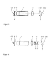
- FIG. 1 in which a microscope M is shown schematically with an object plane 0, a lens 1, a tube lens 2 and an image plane 0 ' FIG. 2 the coupling of this microscope to an image processing module BM.
- the interface S between the microscope M and the image processing module BM is located between the tube lens 2 and the image plane 0 'of the microscope M.
- a structural element (spinning disk) 3 is arranged at a tilt angle ⁇ to the image plane 0', the image 3 'of which is above the transmissive component of the light component emanating from an illumination source BQ in the object plane 0 under the modified by the scale of the optical system, opposite tilt angle ⁇ 'is seen. Furthermore, the light component 4 reflected by the structural element 3 and the transmitted light component 4a are shown.
- FIG. 3 shows in addition to the arrangement of the structural element 3 in the image plane O 'and its image 3' in the object plane 0, the size of the object field OG in the object plane 0 compared to the size of the image OG '(conjugate image of the object field OG) in the image plane 0' ,
- FIG. 4 is the arrangement of the optical adapter 5 with a prism arrangement consisting of two prisms 6 and 7, shown.
- the optical adapter 5 is located between the tube lens 2 and the image plane 0 '.
- the optical adapter 5 causes the image 3 'of the structural element 3 is no longer below the tilt angle ⁇ ' to the object plane 0, but falls directly into the object plane 0.
- the beam path STG is deflected by the arrangement of the prisms 6 and 7 by an angle ⁇ , which in FIG. 5 is shown in more detail.
- the bending angle ⁇ can be influenced by compromise formation of the generated positional change of the image plane by the tilt angle ⁇ 'or the imaging quality (aberrations).
Landscapes
- Physics & Mathematics (AREA)
- Chemical & Material Sciences (AREA)
- Analytical Chemistry (AREA)
- General Physics & Mathematics (AREA)
- Optics & Photonics (AREA)
- Microscoopes, Condenser (AREA)
- Optical Elements Other Than Lenses (AREA)
Abstract
Description
- Die Erfindung betrifft eine Einrichtung für mikroskopische Anwendungen, umfassend ein als Strahlteiler wirkendes, sich drehendes Strukturelement (spinning disk) mit reflektierenden und transmittierenden Strukturen, welches in einer dem Objektfeld konjugierten Ebene (Zwischenbildebene) des Strahlenganges angeordnet ist, dessen Struktur auf ein Objekt in der Objektebene abgebildet wird und das vom Objekt reflektierte oder durch die Beleuchtung hervorgerufene Fluoreszenzlicht wieder auf das Strukturelement trifft sowie einem Bildverarbeitungsmodul (Imaging Modul), wobei das vom Strukturelement reflektierte und transmittierte Strahlenbündel durch das Bildverarbeitungsmodul geführt wird, in dem das Strukturelement unter einem Winkel zur Senkrechten des Strahlenganges gestellt ist.
- Bekannt sind konfokale Mikroskope, bei denen eine punktförmige Lichtquelle auf ein Objekt abgebildet wird oder ein in einer dem Objektfeld konjugierten Ebene befindliches übertragenes, kreisförmiges sowie drehbares Strukturelement mit beispielweise Löchern, Gitterlinien oder andere beliebigen Strukturen (Spinning disk) auf das Objekt abgebildet wird und das am Objekt reflektierte oder durch die Beleuchtung hervorgerufene Fluoreszenzlicht auf dem Rückweg wiederum auf das Strukturelement fällt. Durch die auf dem Strukturelement befindliche reflektierende, musterartig ausgebildete, teiltransmittierende Schicht, wirkt das Strukturelement als Strahlteiler. Typischerweise wird diese Schicht durch eine Metallbedampfung, beispielsweise unter Verwendung von Chrom, Silber, Gold oder Aluminium, hergestellt. Die Metallschicht ist dann hochreflektiv, während die Lücken in der Struktur hochtransmittierend sind. Wird nicht nur das transmittierte Licht für die Bildgebung weiterverwendet, besteht die Aufgabe darin, das reflektierte Strahlenbündel durch das bildgebende Modul zu führen. Dazu wird nach den Lösungen des Standes der Technik das Strukturelement unter einem hinreichenden Winkel zur optischen Achse des Mikroskopsystems in die Zwischenbildebene gestellt, so dass das reflektierte Strahlenbündel vom transmittierten Strahlenbündel separiert weitergeleitet werden kann. Darüber hinaus kann das Strukturelement zur optischen Achse so orientiert sein, dass störende Reflexe im System vermieden werden.
- Ein wesentlicher Nachteil des schief angeordneten Strukturelementes ist, dass die auf das Objekt abgebildete Struktur auch schief abgebildet wird, also die Objektebene und die Ebene des Strukturelementes in einen Winkel zueinander stehen. Im Objektraum ist der resultierende Winkel zwischen diesen Ebenen abhängig von der durch die Mikroskopoptik bewirkten Vergrößerung. Der Effekt ist dabei, dass die Struktur im Objektfeld nicht gleichförmig wirkt und in Abhängigkeit vom Abbildungsmaßstab unterschiedlich ist.
- Ein weiterer Nachteil ist, dass je nach der Größe des Winkels die Schieflage des Strukturelementes die Tiefenschärfe der Abbildung die Wirkung des abgebildeten Struktur nicht mehr für das gesamte Objektfeld vermittelt, sondern nur für einen Teil des Objektfeldes, für den sich das Strukturelement noch in der Tiefenschärfe des optisches Systems befindet. Daraus resultierend wird nicht die Objektebene sondern eine im Winkel dazu befindliche Ebene abgebildet. Ein Seiteneffekt ist die laterale Vergrößerungsänderung über das Bildfeld, von Bildrand zu Bildrand, beziehungsweise ein Trapezeffekt.
- In
DE 195 11 937 AI wird eine Anordnung beschrieben, bei der ein senkrecht im Strahlengang befindliches Strukturelement einen störenden Reflex erzeugt. Dieser Reflex wird nicht als Nutzlicht verwendet. Das Strukturelement steht dabei unter einem Winkel im Strahlengang, der bewirkt, dass der Reflex in einen Raumwinkel gelenkt wird, der nicht zum detektierten Signal beiträgt. Ferner beinhaltet die Lösung die Anordnung eines Prismenpaares, wobei ein Prisma entlang des Strahlverlaufes vor dem Strukturelement liegt und ein Prisma nach dem Strukturelement angeordnet ist. - Nachteil dieser Anordnung ist, dass das reflektierte Strahlenbündel nicht weiterverwendet werden kann, da die Prismen zu nahe am Strukturelement angeordnet sind, so dass das reflektierte Strahlenbündel nicht weiterverwendet werden kann. Weiterhin ist die Prismenanordnung integraler Bestandteil des Abbildungssystems (Imaging-Moduls), beziehungsweise der Tubuseinheit.
- Ein weiterer erheblicher Nachteil ist die durch die geometrische Anordnung der Prismen bedingte und für die vorliegende Anwendung ungenügende Abbildungsqualität. Die hauptsächlichen Fehler sind dabei Astigmatismus und Farbquerfehler.
- Die in
EP 1 145 067 B1 realisierte Anordnung geht einen Kompromiss ein, der den Winkel zwischen der Ebene des Strukturelementes und der Zwischenbildebene gerade so groß wählt, dass das halbe Sehfeld bei relativ geringer numerischer Apertur beziehungsweise Auflösungsvermögen des Gesamtsystems auf die Detektoren geführt werden kann, ohne dass die oben genannte Effekte zum Tragen kommen. - Ausgehend von den Nachteilen der bekannten Lösungen liegt der Erfindung die Aufgabe zugrunde, eine Einrichtung für mikroskopische Anwendungen dahingehend weiter zu bilden, dass in Reflexion und Transmission das volle Sehfeld bei voller numerischer Apertur auf die Detektoren übertragen wird.
- Diese Aufgabe wird erfindungsgemäß mit einer Einrichtung der eingangs beschriebenen Art durch die Merkmale des Patentanspruchs 1 gelöst. Vorteilhafte Ausgestaltungen sind in den Unteransprüchen 2 bis 7 angegeben.
- Erfindungsgemäß ist an der Schnittstelle zwischen dem Mikroskop und dem Bildverarbeitungsmodul ein optischer Adapter angeordnet, der das mikroskopische Zwischenbild auf die Bildebene des als Strahlteiler wirkenden Strukturelementes kippt.
- Dabei benötigen das Mikroskop sowie das Bildverarbeitungsmodul keine Änderung ihrer internen Optik, das heißt der Strahlengang vor und nach dem optischen Adapter im Mikroskop und Bildverarbeitungsmodul bleibt unverändert.
- Die erfindungsgemäße Anordnung des optischen Adapters erzeugt eine hohe Abbildungsgüte (Strehl'sche Definitionshelligkeit).
- Vorteilhafterweise ist der optische Adapter als Prismenanordnung ausgebildet.
- In einer vorteilhaften Ausgestaltung beträgt der Knickwinkel an der Schnittstelle zwischen dem Mikroskop und dem Bildverarbeitungsmodul bei einer Kippung der Bildebene um 8 Grad etwa 4,5 Grad.
- Wird darauf verzichtet, das gesamte Sehfeld innerhalb einer Tiefenschärfe längs der Orientierung des Strukturelementes auszurichten, können auch andere Winkel eingestellt werden, die eventuelle Randbedingungen besser bedienen, beispielsweise baulicher Natur. Es ist auch denkbar, dass der Winkel von der Fertigbarkeit der Prismen, der Glasauswahl und zulässiger Toleranzen abhängt.
- Der optische Adapter kann je nach Anwendung mit dem Bildverarbeitungsmodul fest oder lösbar verbunden sein.
- Es kann auch von Vorteil sein, wenn der optische Adapter Bestandteil des Gesamtsystems von Mikroskop und Bildverarbeitungsmodul ist. In diesem Fall wäre von außen nur eine einzige Komponente wahrzunehmen.
- Die erfindungsgemäße Einrichtung für mikroskopische Anwendungen soll nachfolgend anhand eines Ausführungsbeispiels näher erläutert werden. Dazu zeigen:
- Figur 1:
- eine schematische, vereinfachte Darstellung der Einrichtung,
- Figur 2:
- eine schematische Darstellung der Strahlengänge des Mikroskops und des Bildverarbeitungsmoduls und deren Kopplung,
- Figur 3:
- eine schematische Darstellung der Objektfeldgröße und der Bildgröße,
- Figur 4:
- eine schematische Darstellung des optischen Adapters und
- Figur 5:
- eine vergrößerte Darstellung des optischen Adapters.
- Ausgehend von
Figur 1 , in der schematisch ein Mikroskop M mit einer Objektebene 0, einem Objektiv 1, einer Tubuslinse 2 und einer Bildebene 0' dargestellt ist, zeigtFigur 2 die Ankopplung dieses Mikroskops an ein Bildverarbeitungsmodul BM. Die Schnittstelle S zwischen dem Mikroskop M und dem Bildverarbeitungsmodul BM befindet sich dabei zwischen der Tubuslinse 2 und der Bildebene 0' des Mikroskops M. - Am Ort der Bildebene 0' ist unter einem Kippwinkel α zur Bildebene 0' ein Strukturelement (Spinning Disk) 3 angeordnet, dessen Bild 3' über den transmittierenden Anteil des von einer Beleuchtungsquelle BQ ausgehenden Lichtanteils in der Objektebene 0 unter dem durch den Maßstab des optischen Systems modifizierten, entgegengesetzten Kippwinkel α' zu sehen ist. Ferner ist der vom Strukturelement 3 reflektierte Lichtanteil 4 und der transmittierte Lichtanteil 4a dargestellt.
-
Figur 3 zeigt neben der Anordnung des Strukturelementes 3 in der Bildebene O' und dessen Bild 3' in der Objektebene 0 die Größe des Objektfeldes OG in der Objektebene 0 im Vergleich zur Größe des Bildes OG' (konjugiertes Bild des Objektfeldes OG) in der Bildebene 0'. - In
Figur 4 ist die Anordnung des optischen Adapters 5 mit einer Prismenanordnung, bestehend aus zwei Prismen 6 und 7, dargestellt. Der optische Adapter 5 befindet sich dabei zwischen der Tubuslinse 2 und der Bildebene 0'. Der optische Adapter 5 bewirkt, dass das Bild 3'des Strukturelementes 3 nicht mehr unter dem Kippwinkel α' zur Objektebene 0 steht, sondern direkt in die Objektebene 0 fällt. Der Strahlengang STG wird durch die Anordnung der Prismen 6 und 7 um einen Winkel β umgelenkt, was inFigur 5 näher dargestellt ist. - Wie bereits ausgeführt, zeigt
Figur 5 die detailliertere Ansicht des optischen Adapters 5, durch den es mittels der Prismen 6 und 7 zu einer Knickung des Strahlenganges STG um einen Winkel β und zu einer Kippung der Bildebene 0' relativ zur neuen Lage des Strahlenganges STG um einen Winkel α=β' kommt. - Dabei erfolgt mittels des Prismas 7 eine Kompensation der Wirkung des Prismas 6 bezüglich Koma und Farbquerfehler, aber nicht bezüglich der Bildebenenkippung. Das ist möglich, da die Kippung der Bildebene O' nicht von der axialen Position der Prismen 6 und 7 oder deren Abstand, sondern nur von deren Ablenkwinkel bedingt ist. Koma und Farbquerfehler reagieren hingegen deutlich auch auf die Position der beiden Prismen 6 und 7. Somit kann eine Kippung der Bildebene 0' erzeugt werden ohne dass dabei Koma und Farbquerfehler erzeugt wird, und zwar über den Abstand der beiden Prismen 6 und 7 zueinander und über den Abstand zur Bildebene 0' selbst. Andere Aberrationen sind bei dem Aufbau ohnehin klein und in der Betrachtung vernachlässigbar.
- Bei einem Knickwinkel β von 4,5 Grad ergibt sich eine Kippung der Bildebene 0' um den Kippwinkel β' von 8 Grad.
- Der Knickwinkel β lässt sich beeinflussen unter Kompromissbildung der erzeugten Lageveränderung der Bildebene um den Kippwinkel β' oder der Abbildungsgüte (Aberrationen).
-
- 1
- Objektiv
- 2
- Tubuslinse
- 3
- Strukturelement
- 3'
- Bild des Strukturelementes
- 4
- reflektierter Lichtanteil
- 4a
- transmittierter Lichtanteil
- 5
- optischer Adapter
- 6, 7
- Prisma
- 0
- Objektebene
- 0'
- Bildebene
- M
- Mikroskop
- S
- Schnittstelle
- STG
- Strahlengang
- BM
- Bildverarbeitungsmodul
- BQ
- Beleuchtungsquelle
- α, α',β'
- Kippwinkel
- β
- Knickwinkel
Claims (7)
- Einrichtung für mikroskopische Anwendungen, umfassend ein als Strahlteiler wirkendes, sich drehendes Strukturelement (3) (spinning disk) mit reflektierenden (4) und transmittierenden Strukturen, welches in einer dem Objektfeld konjugierten Ebene 0'(Zwischenbildebene) des Strahlenganges angeordnet ist, dessen Struktur auf ein Objekt (3') in der Objektebene (O) abgebildet wird und das vom Objekt (3') reflektierte oder durch die Beleuchtung hervorgerufene Fluoreszenzlicht wieder auf das Strukturelement (3) trifft sowie einem Bildverarbeitungsmodul (BM) (Imaging Modul), wobei das vom Strukturelement (3) reflektierte und transmittierte Strahlenbündel (4) durch das Bildverarbeitungsmodul (BM) geführt wird, in dem das Strukturelement (3) unter einem Winkel (α) zur Senkrechten des Strahlenganges (STG) gestellt ist, dadurch gekennzeichnet, dass an der Schnittstelle (S) zwischen dem Mikroskop (M) und dem Bildverarbeitungsmodul (BM) ein optischer Adapter (5) angeordnet ist, der das mikroskopische Zwischenbild (0') auf die Ebene des als Strahlteiler wirkenden Strukturelementes (3) kippt.
- Einrichtung für mikroskopische Anwendungen nach Anspruch 1, dadurch gekennzeichnet, dass der optische Adapter (5) als Prismenanordnung (6,7) ausgebildet ist.
- Einrichtung für mikroskopische Anwendungen nach den Ansprüche 1 und 2, dadurch gekennzeichnet, dass der Knickwinkel (β) an der Schnittstelle (S) zwischen dem Mikroskop (M) und dem Bildverarbeitungsmodul (BM) bei einer Kippung der Bildebene (O') um den Kippwinkel (β') 8 Grad etwa 4,5 Grad ist.
- Einrichtung für mikroskopische Anwendungen nach den Ansprüchen 1 bis 3, dadurch gekennzeichnet, dass der optische Adapter (5) mit dem Bildverarbeitungsmodul (BM) fest verbunden ist.
- Einrichtung für mikroskopische Anwendungen nach den Ansprüchen 1 bis 3, dadurch gekennzeichnet, dass der optische Adapter (5) vom Bildverarbeitungsmodul (BM) lösbar ist.
- Einrichtung für mikroskopische Anwendungen Nach den Ansprüchen 1 bis 3, dadurch gekennzeichnet, dass der optische Adapter (5) integraler Bestandteil des Gesamtsystems von Mikroskop (M) und Bildverarbeitungsmodul (BM) ist.
- Einrichtung für mikroskopische Anwendungen nach den Ansprüchen 1 bis 6, dadurch gekennzeichnet, dass sie für den Bereich der konfokalen Bildgebung vorgesehen ist.
Applications Claiming Priority (1)
| Application Number | Priority Date | Filing Date | Title |
|---|---|---|---|
| DE102014005309.1A DE102014005309A1 (de) | 2014-04-10 | 2014-04-10 | Einrichtung für mikroskopische Anwendungen |
Publications (2)
| Publication Number | Publication Date |
|---|---|
| EP2930548A1 true EP2930548A1 (de) | 2015-10-14 |
| EP2930548B1 EP2930548B1 (de) | 2018-08-01 |
Family
ID=52807692
Family Applications (1)
| Application Number | Title | Priority Date | Filing Date |
|---|---|---|---|
| EP15162308.9A Not-in-force EP2930548B1 (de) | 2014-04-10 | 2015-04-02 | Einrichtung für mikroskopische anwendungen |
Country Status (3)
| Country | Link |
|---|---|
| US (1) | US9857579B2 (de) |
| EP (1) | EP2930548B1 (de) |
| DE (1) | DE102014005309A1 (de) |
Citations (6)
| Publication number | Priority date | Publication date | Assignee | Title |
|---|---|---|---|---|
| US4850686A (en) * | 1987-02-06 | 1989-07-25 | Asahi Kogaku Kogyo K.K. | Apparatus for adjusting light beam direction |
| US5022743A (en) * | 1987-03-27 | 1991-06-11 | The Board Of Trustees Of The Leland Stanford Junior University | Scanning confocal optical microscope |
| DE19511937A1 (de) | 1995-03-31 | 1996-10-02 | Zeiss Carl Jena Gmbh | Konfokales Auflichtmikroskop |
| US5861984A (en) * | 1995-03-31 | 1999-01-19 | Carl Zeiss Jena Gmbh | Confocal scanning microscope and beamsplitter therefor |
| DE19835073A1 (de) * | 1998-08-04 | 2000-02-10 | Zeiss Carl Jena Gmbh | Mikroskop mit Auflichteinkopplung |
| EP1145067B1 (de) | 1999-01-22 | 2002-09-04 | Isis Innovation Limited | Vorrichtung und verfahren zur konfokalen mikroskopie |
Family Cites Families (4)
| Publication number | Priority date | Publication date | Assignee | Title |
|---|---|---|---|---|
| DE59609547D1 (de) * | 1995-05-17 | 2002-09-12 | Leica Mikroskopie Systeme Ag H | Mikroskop |
| US5915048A (en) * | 1996-06-05 | 1999-06-22 | Zetetic Institute | Method and apparatus for discriminating in-focus images from out-of-focus light signals from background and foreground light sources |
| JP3727543B2 (ja) * | 2000-05-10 | 2005-12-14 | 三菱電機株式会社 | 画像表示装置 |
| US8610902B2 (en) * | 2011-06-02 | 2013-12-17 | Asm Technology Singapore Pte Ltd | Apparatus and method for inspecting an object with increased depth of field |
-
2014
- 2014-04-10 DE DE102014005309.1A patent/DE102014005309A1/de not_active Withdrawn
-
2015
- 2015-04-02 EP EP15162308.9A patent/EP2930548B1/de not_active Not-in-force
- 2015-04-09 US US14/683,007 patent/US9857579B2/en not_active Expired - Fee Related
Patent Citations (6)
| Publication number | Priority date | Publication date | Assignee | Title |
|---|---|---|---|---|
| US4850686A (en) * | 1987-02-06 | 1989-07-25 | Asahi Kogaku Kogyo K.K. | Apparatus for adjusting light beam direction |
| US5022743A (en) * | 1987-03-27 | 1991-06-11 | The Board Of Trustees Of The Leland Stanford Junior University | Scanning confocal optical microscope |
| DE19511937A1 (de) | 1995-03-31 | 1996-10-02 | Zeiss Carl Jena Gmbh | Konfokales Auflichtmikroskop |
| US5861984A (en) * | 1995-03-31 | 1999-01-19 | Carl Zeiss Jena Gmbh | Confocal scanning microscope and beamsplitter therefor |
| DE19835073A1 (de) * | 1998-08-04 | 2000-02-10 | Zeiss Carl Jena Gmbh | Mikroskop mit Auflichteinkopplung |
| EP1145067B1 (de) | 1999-01-22 | 2002-09-04 | Isis Innovation Limited | Vorrichtung und verfahren zur konfokalen mikroskopie |
Also Published As
| Publication number | Publication date |
|---|---|
| EP2930548B1 (de) | 2018-08-01 |
| US9857579B2 (en) | 2018-01-02 |
| US20150293338A1 (en) | 2015-10-15 |
| DE102014005309A1 (de) | 2015-10-15 |
Similar Documents
| Publication | Publication Date | Title |
|---|---|---|
| DE2051174B2 (de) | Doppelmikroskop | |
| EP2185953B1 (de) | Lichtfalle, einkoppeleinrichtung für einen strahlengang sowie beleuchtungseinrichtung und optische beobachtungseinrichtung | |
| DE102014110606A1 (de) | Mikroskop mit einer Strahlteileranordnung | |
| EP3198323B2 (de) | Vorrichtung zur abbildung einer probe | |
| EP1285305A1 (de) | Autofokussiereinrichtung für optische geräte | |
| DE102014118025B4 (de) | Vorrichtung zur Lichtblattmikroskopie | |
| CH653446A5 (de) | Spiegellinsenobjektiv von hohem oeffnungsverhaeltnis. | |
| WO2008077579A1 (de) | Mehrkanaliger optischer drehübertrager mit hoher rückflussdämpfung | |
| DE102007046872B4 (de) | Optische Abbildungsvorrichtung | |
| EP1019770A1 (de) | Mikroskop mit auflichteinkopplung | |
| EP2930548B1 (de) | Einrichtung für mikroskopische anwendungen | |
| DE10300455A1 (de) | Tubus zur Adaption an ein Mikroskop | |
| DE102010015506A1 (de) | Katadioptrisches Cassegrain-Objektiv | |
| DE102014017003A1 (de) | Scaneinrichtung zur 3D-Positionierung von Laserspots | |
| EP3168671A1 (de) | Beleuchtungsanordnung | |
| DE102005037764B4 (de) | Anordnung zur homogenen Beleuchtung eines Feldes | |
| CH651944A5 (de) | Koehlersche auflicht-hellfeld-beleuchtungseinrichtung. | |
| WO2016116424A2 (de) | Optische anordnung für ein laser-scanner-system | |
| DE2458720A1 (de) | Vorrichtung zum kippen eines feldes in optischen systemen | |
| DE102014108596B3 (de) | Objektiv und optisches Gerät | |
| DE19921227B4 (de) | Konvergenztubus | |
| DE109091C (de) | ||
| LU92846B1 (de) | Verfahren und Beleuchtungsanordnung zum Beleuchten einer Probenschicht mit einem Lichtblatt | |
| DE102016209524B4 (de) | Verlaufsfilteranordnung, optische Anordnung umfassend eine Verlaufsfilteranordnung und Verwendung einer Verlaufsfilteranordnung | |
| DE2021654C2 (de) | Floureszenzauflichtilluminator |
Legal Events
| Date | Code | Title | Description |
|---|---|---|---|
| PUAI | Public reference made under article 153(3) epc to a published international application that has entered the european phase |
Free format text: ORIGINAL CODE: 0009012 |
|
| 17P | Request for examination filed |
Effective date: 20150402 |
|
| AK | Designated contracting states |
Kind code of ref document: A1 Designated state(s): AL AT BE BG CH CY CZ DE DK EE ES FI FR GB GR HR HU IE IS IT LI LT LU LV MC MK MT NL NO PL PT RO RS SE SI SK SM TR |
|
| AX | Request for extension of the european patent |
Extension state: BA ME |
|
| STAA | Information on the status of an ep patent application or granted ep patent |
Free format text: STATUS: EXAMINATION IS IN PROGRESS |
|
| 17Q | First examination report despatched |
Effective date: 20170206 |
|
| GRAP | Despatch of communication of intention to grant a patent |
Free format text: ORIGINAL CODE: EPIDOSNIGR1 |
|
| STAA | Information on the status of an ep patent application or granted ep patent |
Free format text: STATUS: GRANT OF PATENT IS INTENDED |
|
| INTG | Intention to grant announced |
Effective date: 20180323 |
|
| GRAS | Grant fee paid |
Free format text: ORIGINAL CODE: EPIDOSNIGR3 |
|
| GRAA | (expected) grant |
Free format text: ORIGINAL CODE: 0009210 |
|
| STAA | Information on the status of an ep patent application or granted ep patent |
Free format text: STATUS: THE PATENT HAS BEEN GRANTED |
|
| AK | Designated contracting states |
Kind code of ref document: B1 Designated state(s): AL AT BE BG CH CY CZ DE DK EE ES FI FR GB GR HR HU IE IS IT LI LT LU LV MC MK MT NL NO PL PT RO RS SE SI SK SM TR |
|
| REG | Reference to a national code |
Ref country code: GB Ref legal event code: FG4D Free format text: NOT ENGLISH |
|
| REG | Reference to a national code |
Ref country code: CH Ref legal event code: EP Ref country code: AT Ref legal event code: REF Ref document number: 1024966 Country of ref document: AT Kind code of ref document: T Effective date: 20180815 |
|
| REG | Reference to a national code |
Ref country code: IE Ref legal event code: FG4D Free format text: LANGUAGE OF EP DOCUMENT: GERMAN |
|
| REG | Reference to a national code |
Ref country code: DE Ref legal event code: R096 Ref document number: 502015005268 Country of ref document: DE |
|
| REG | Reference to a national code |
Ref country code: NL Ref legal event code: MP Effective date: 20180801 |
|
| REG | Reference to a national code |
Ref country code: LT Ref legal event code: MG4D |
|
| PG25 | Lapsed in a contracting state [announced via postgrant information from national office to epo] |
Ref country code: FI Free format text: LAPSE BECAUSE OF FAILURE TO SUBMIT A TRANSLATION OF THE DESCRIPTION OR TO PAY THE FEE WITHIN THE PRESCRIBED TIME-LIMIT Effective date: 20180801 Ref country code: NO Free format text: LAPSE BECAUSE OF FAILURE TO SUBMIT A TRANSLATION OF THE DESCRIPTION OR TO PAY THE FEE WITHIN THE PRESCRIBED TIME-LIMIT Effective date: 20181101 Ref country code: GR Free format text: LAPSE BECAUSE OF FAILURE TO SUBMIT A TRANSLATION OF THE DESCRIPTION OR TO PAY THE FEE WITHIN THE PRESCRIBED TIME-LIMIT Effective date: 20181102 Ref country code: IS Free format text: LAPSE BECAUSE OF FAILURE TO SUBMIT A TRANSLATION OF THE DESCRIPTION OR TO PAY THE FEE WITHIN THE PRESCRIBED TIME-LIMIT Effective date: 20181201 Ref country code: PL Free format text: LAPSE BECAUSE OF FAILURE TO SUBMIT A TRANSLATION OF THE DESCRIPTION OR TO PAY THE FEE WITHIN THE PRESCRIBED TIME-LIMIT Effective date: 20180801 Ref country code: LT Free format text: LAPSE BECAUSE OF FAILURE TO SUBMIT A TRANSLATION OF THE DESCRIPTION OR TO PAY THE FEE WITHIN THE PRESCRIBED TIME-LIMIT Effective date: 20180801 Ref country code: RS Free format text: LAPSE BECAUSE OF FAILURE TO SUBMIT A TRANSLATION OF THE DESCRIPTION OR TO PAY THE FEE WITHIN THE PRESCRIBED TIME-LIMIT Effective date: 20180801 Ref country code: NL Free format text: LAPSE BECAUSE OF FAILURE TO SUBMIT A TRANSLATION OF THE DESCRIPTION OR TO PAY THE FEE WITHIN THE PRESCRIBED TIME-LIMIT Effective date: 20180801 Ref country code: SE Free format text: LAPSE BECAUSE OF FAILURE TO SUBMIT A TRANSLATION OF THE DESCRIPTION OR TO PAY THE FEE WITHIN THE PRESCRIBED TIME-LIMIT Effective date: 20180801 Ref country code: BG Free format text: LAPSE BECAUSE OF FAILURE TO SUBMIT A TRANSLATION OF THE DESCRIPTION OR TO PAY THE FEE WITHIN THE PRESCRIBED TIME-LIMIT Effective date: 20181101 |
|
| PG25 | Lapsed in a contracting state [announced via postgrant information from national office to epo] |
Ref country code: AL Free format text: LAPSE BECAUSE OF FAILURE TO SUBMIT A TRANSLATION OF THE DESCRIPTION OR TO PAY THE FEE WITHIN THE PRESCRIBED TIME-LIMIT Effective date: 20180801 Ref country code: HR Free format text: LAPSE BECAUSE OF FAILURE TO SUBMIT A TRANSLATION OF THE DESCRIPTION OR TO PAY THE FEE WITHIN THE PRESCRIBED TIME-LIMIT Effective date: 20180801 Ref country code: LV Free format text: LAPSE BECAUSE OF FAILURE TO SUBMIT A TRANSLATION OF THE DESCRIPTION OR TO PAY THE FEE WITHIN THE PRESCRIBED TIME-LIMIT Effective date: 20180801 |
|
| PG25 | Lapsed in a contracting state [announced via postgrant information from national office to epo] |
Ref country code: ES Free format text: LAPSE BECAUSE OF FAILURE TO SUBMIT A TRANSLATION OF THE DESCRIPTION OR TO PAY THE FEE WITHIN THE PRESCRIBED TIME-LIMIT Effective date: 20180801 Ref country code: CZ Free format text: LAPSE BECAUSE OF FAILURE TO SUBMIT A TRANSLATION OF THE DESCRIPTION OR TO PAY THE FEE WITHIN THE PRESCRIBED TIME-LIMIT Effective date: 20180801 Ref country code: IT Free format text: LAPSE BECAUSE OF FAILURE TO SUBMIT A TRANSLATION OF THE DESCRIPTION OR TO PAY THE FEE WITHIN THE PRESCRIBED TIME-LIMIT Effective date: 20180801 Ref country code: RO Free format text: LAPSE BECAUSE OF FAILURE TO SUBMIT A TRANSLATION OF THE DESCRIPTION OR TO PAY THE FEE WITHIN THE PRESCRIBED TIME-LIMIT Effective date: 20180801 Ref country code: EE Free format text: LAPSE BECAUSE OF FAILURE TO SUBMIT A TRANSLATION OF THE DESCRIPTION OR TO PAY THE FEE WITHIN THE PRESCRIBED TIME-LIMIT Effective date: 20180801 |
|
| REG | Reference to a national code |
Ref country code: DE Ref legal event code: R097 Ref document number: 502015005268 Country of ref document: DE |
|
| PG25 | Lapsed in a contracting state [announced via postgrant information from national office to epo] |
Ref country code: SM Free format text: LAPSE BECAUSE OF FAILURE TO SUBMIT A TRANSLATION OF THE DESCRIPTION OR TO PAY THE FEE WITHIN THE PRESCRIBED TIME-LIMIT Effective date: 20180801 Ref country code: DK Free format text: LAPSE BECAUSE OF FAILURE TO SUBMIT A TRANSLATION OF THE DESCRIPTION OR TO PAY THE FEE WITHIN THE PRESCRIBED TIME-LIMIT Effective date: 20180801 Ref country code: SK Free format text: LAPSE BECAUSE OF FAILURE TO SUBMIT A TRANSLATION OF THE DESCRIPTION OR TO PAY THE FEE WITHIN THE PRESCRIBED TIME-LIMIT Effective date: 20180801 |
|
| PLBE | No opposition filed within time limit |
Free format text: ORIGINAL CODE: 0009261 |
|
| STAA | Information on the status of an ep patent application or granted ep patent |
Free format text: STATUS: NO OPPOSITION FILED WITHIN TIME LIMIT |
|
| 26N | No opposition filed |
Effective date: 20190503 |
|
| PG25 | Lapsed in a contracting state [announced via postgrant information from national office to epo] |
Ref country code: SI Free format text: LAPSE BECAUSE OF FAILURE TO SUBMIT A TRANSLATION OF THE DESCRIPTION OR TO PAY THE FEE WITHIN THE PRESCRIBED TIME-LIMIT Effective date: 20180801 |
|
| REG | Reference to a national code |
Ref country code: CH Ref legal event code: PL |
|
| REG | Reference to a national code |
Ref country code: BE Ref legal event code: MM Effective date: 20190430 |
|
| PG25 | Lapsed in a contracting state [announced via postgrant information from national office to epo] |
Ref country code: LU Free format text: LAPSE BECAUSE OF NON-PAYMENT OF DUE FEES Effective date: 20190402 Ref country code: MC Free format text: LAPSE BECAUSE OF FAILURE TO SUBMIT A TRANSLATION OF THE DESCRIPTION OR TO PAY THE FEE WITHIN THE PRESCRIBED TIME-LIMIT Effective date: 20180801 |
|
| PG25 | Lapsed in a contracting state [announced via postgrant information from national office to epo] |
Ref country code: LI Free format text: LAPSE BECAUSE OF NON-PAYMENT OF DUE FEES Effective date: 20190430 Ref country code: CH Free format text: LAPSE BECAUSE OF NON-PAYMENT OF DUE FEES Effective date: 20190430 |
|
| PG25 | Lapsed in a contracting state [announced via postgrant information from national office to epo] |
Ref country code: BE Free format text: LAPSE BECAUSE OF NON-PAYMENT OF DUE FEES Effective date: 20190430 |
|
| PG25 | Lapsed in a contracting state [announced via postgrant information from national office to epo] |
Ref country code: TR Free format text: LAPSE BECAUSE OF FAILURE TO SUBMIT A TRANSLATION OF THE DESCRIPTION OR TO PAY THE FEE WITHIN THE PRESCRIBED TIME-LIMIT Effective date: 20180801 |
|
| PG25 | Lapsed in a contracting state [announced via postgrant information from national office to epo] |
Ref country code: IE Free format text: LAPSE BECAUSE OF NON-PAYMENT OF DUE FEES Effective date: 20190402 |
|
| PG25 | Lapsed in a contracting state [announced via postgrant information from national office to epo] |
Ref country code: PT Free format text: LAPSE BECAUSE OF FAILURE TO SUBMIT A TRANSLATION OF THE DESCRIPTION OR TO PAY THE FEE WITHIN THE PRESCRIBED TIME-LIMIT Effective date: 20181201 |
|
| PGFP | Annual fee paid to national office [announced via postgrant information from national office to epo] |
Ref country code: FR Payment date: 20200420 Year of fee payment: 6 Ref country code: DE Payment date: 20200420 Year of fee payment: 6 |
|
| PGFP | Annual fee paid to national office [announced via postgrant information from national office to epo] |
Ref country code: GB Payment date: 20200427 Year of fee payment: 6 |
|
| PG25 | Lapsed in a contracting state [announced via postgrant information from national office to epo] |
Ref country code: CY Free format text: LAPSE BECAUSE OF FAILURE TO SUBMIT A TRANSLATION OF THE DESCRIPTION OR TO PAY THE FEE WITHIN THE PRESCRIBED TIME-LIMIT Effective date: 20180801 |
|
| REG | Reference to a national code |
Ref country code: AT Ref legal event code: MM01 Ref document number: 1024966 Country of ref document: AT Kind code of ref document: T Effective date: 20200402 |
|
| PG25 | Lapsed in a contracting state [announced via postgrant information from national office to epo] |
Ref country code: MT Free format text: LAPSE BECAUSE OF FAILURE TO SUBMIT A TRANSLATION OF THE DESCRIPTION OR TO PAY THE FEE WITHIN THE PRESCRIBED TIME-LIMIT Effective date: 20180801 Ref country code: HU Free format text: LAPSE BECAUSE OF FAILURE TO SUBMIT A TRANSLATION OF THE DESCRIPTION OR TO PAY THE FEE WITHIN THE PRESCRIBED TIME-LIMIT; INVALID AB INITIO Effective date: 20150402 |
|
| PG25 | Lapsed in a contracting state [announced via postgrant information from national office to epo] |
Ref country code: AT Free format text: LAPSE BECAUSE OF NON-PAYMENT OF DUE FEES Effective date: 20200402 |
|
| REG | Reference to a national code |
Ref country code: DE Ref legal event code: R119 Ref document number: 502015005268 Country of ref document: DE |
|
| GBPC | Gb: european patent ceased through non-payment of renewal fee |
Effective date: 20210402 |
|
| PG25 | Lapsed in a contracting state [announced via postgrant information from national office to epo] |
Ref country code: DE Free format text: LAPSE BECAUSE OF NON-PAYMENT OF DUE FEES Effective date: 20211103 Ref country code: GB Free format text: LAPSE BECAUSE OF NON-PAYMENT OF DUE FEES Effective date: 20210402 Ref country code: FR Free format text: LAPSE BECAUSE OF NON-PAYMENT OF DUE FEES Effective date: 20210430 |
|
| PG25 | Lapsed in a contracting state [announced via postgrant information from national office to epo] |
Ref country code: MK Free format text: LAPSE BECAUSE OF FAILURE TO SUBMIT A TRANSLATION OF THE DESCRIPTION OR TO PAY THE FEE WITHIN THE PRESCRIBED TIME-LIMIT Effective date: 20180801 |