EP2929405B1 - Spring-loaded supports for head set computer - Google Patents
Spring-loaded supports for head set computer Download PDFInfo
- Publication number
- EP2929405B1 EP2929405B1 EP13812293.2A EP13812293A EP2929405B1 EP 2929405 B1 EP2929405 B1 EP 2929405B1 EP 13812293 A EP13812293 A EP 13812293A EP 2929405 B1 EP2929405 B1 EP 2929405B1
- Authority
- EP
- European Patent Office
- Prior art keywords
- head
- user
- regions
- housing
- worn computer
- Prior art date
- Legal status (The legal status is an assumption and is not a legal conclusion. Google has not performed a legal analysis and makes no representation as to the accuracy of the status listed.)
- Active
Links
Images


Classifications
-
- G—PHYSICS
- G06—COMPUTING OR CALCULATING; COUNTING
- G06F—ELECTRIC DIGITAL DATA PROCESSING
- G06F1/00—Details not covered by groups G06F3/00 - G06F13/00 and G06F21/00
- G06F1/16—Constructional details or arrangements
- G06F1/1613—Constructional details or arrangements for portable computers
- G06F1/163—Wearable computers, e.g. on a belt
-
- G—PHYSICS
- G02—OPTICS
- G02B—OPTICAL ELEMENTS, SYSTEMS OR APPARATUS
- G02B27/00—Optical systems or apparatus not provided for by any of the groups G02B1/00 - G02B26/00, G02B30/00
- G02B27/01—Head-up displays
- G02B27/017—Head mounted
-
- G—PHYSICS
- G02—OPTICS
- G02B—OPTICAL ELEMENTS, SYSTEMS OR APPARATUS
- G02B27/00—Optical systems or apparatus not provided for by any of the groups G02B1/00 - G02B26/00, G02B30/00
- G02B27/01—Head-up displays
- G02B27/017—Head mounted
- G02B27/0176—Head mounted characterised by mechanical features
-
- G—PHYSICS
- G02—OPTICS
- G02B—OPTICAL ELEMENTS, SYSTEMS OR APPARATUS
- G02B27/00—Optical systems or apparatus not provided for by any of the groups G02B1/00 - G02B26/00, G02B30/00
- G02B27/01—Head-up displays
- G02B27/0101—Head-up displays characterised by optical features
- G02B2027/0138—Head-up displays characterised by optical features comprising image capture systems, e.g. camera
-
- G—PHYSICS
- G02—OPTICS
- G02B—OPTICAL ELEMENTS, SYSTEMS OR APPARATUS
- G02B27/00—Optical systems or apparatus not provided for by any of the groups G02B1/00 - G02B26/00, G02B30/00
- G02B27/01—Head-up displays
- G02B27/0101—Head-up displays characterised by optical features
- G02B2027/014—Head-up displays characterised by optical features comprising information/image processing systems
Definitions
- a head mounted computer includes a display and is mounted to a user's head to enable the user to view the display.
- the display shows images to the user which can be generated by, for example, the head mounted computer, anther computer, or a remote device.
- the user can control the head mounted computer or another remote device, which in turn affects the images shown on the display.
- US 2011/089207 is background art and discloses a mounting device couplable to a human head.
- WO 95/11473 is background art and discloses a head-mounted display system.
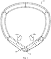
- FIG. 1 is a diagram illustrating a top-down view of an example head worn computer in a partially folded state.
- the head worn computer is comprised of a housing 101, which terminates in two end regions 100.
- the housing may be constructed of a plastic or metal material which encloses all or part of a spring.
- the spring provides an inward force directed towards a user's head.
- the user can apply a force in the direction of arrows 102a-b.
- a first end 100 rests on top of a second end 100 when in a partially folded state.
- the second end 100 may rest on top of the first end 100.
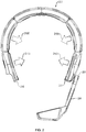
- FIG. 2 is a diagram illustrating an example embodiment of a head worn computer configured to the head of a user.
- the housing 202 rests and remains stationary against the back of the user's head.
- the springs exert an inward force in a direction indicated by arrows 210a-d.
- the inward force secures the computer to the user's head.
- padding may be attached to provide comfort to the user.
- One or more speakers may be attached to the housing, for example, along the outside surface of the housing.
- the speakers may rotate up to 220°. Providing and enabling more than one speaker may provide the user with stereo audio.
- one or both end regions 200 may include a mount 201.
- the mount 201 may be used to attach accessories, such as a camera, a microphone, a sensor, an illumination device, or a display.
- the mounts on each of the end regions can also provide a setup for a strap mount, which can secure the headset computer to the user's head in a more effective manner.
- the mount 201 may also include at least one pivot and/or joint to allow the user to adjust the angle or location of the accessory attached to the mount.
- the head worn computer is mounted with a display 203 attached to an arm 204.
- the display, as well as other accessories, can flip 180°. Flipping the display or accessory allows the user to flip the entire head worn computer and position an accessory on the opposite side of the user's head. This, for example, provides the user with the freedom to shift the display from left eye to right eye, or vice versa, without the need to disconnect and reconnect the display to the opposite mount.
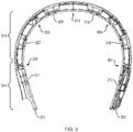
- FIG. 3 is a diagram illustrating a cross-section of an example embodiment of a head worn computer.
- the head worn computer in FIG. 3 includes flexible regions 303-305, stiff regions 307-312, and two end regions 301-302.
- Each flexible region 303-305 includes a spring.
- the springs of each flexible region 303-305 produce an inward force directed towards a user's head.
- the head worn computer may employ multiple springs or it may use one spring to provide a desired amount of inward tension/force.
- a plurality of regions may include at least one flexible region and/or at least one stiff region, or, a plurality of regions may include multiple flexible regions and/or multiple stiff regions.
- a first of the plurality of regions 314 and a second of the plurality of regions 315 can each include at least one flexible region and at least one stiff region.
- the head worn computer includes two sets of flexible regions.
- a first set of flexible regions 305 and 306 are one spring length away from the center of the housing 313.
- the second set of flexible regions 303 and 304 are one spring length away from the first set of flexible regions 305 and 306, and two spring lengths away from center of the housing 313.
- the second set of flexible regions 303 and 304 exerts less force than a single spring in isolation because the second set is two spring lengths from the center of the housing 313.
- the second set of flexible regions 303 and 304 therefore, apply less force than the first set of flexible regions 305 and 306.
- the end regions 301 and 302 when worn by the user, rest near the front of the user's head, above the ear.
- the second set of flexible regions 303 and 304 apply less force than the first flexible regions 305 and 306 to prevent discomfort to the user.
- a near field communication (NFC) link may be installed in one of the plurality of regions.
- a central processing printed circuit board (CPUPCB) including a central processing unit (CPU) coupled to a first near field communications (NFC) module may be installed.
- a second of the regions 315 Adjacent to, or otherwise within range of, the first of the regions 314, a second of the regions 315 may have an auxiliary printed circuit board (AUXPCB) including one or more auxiliary modules operatively coupled to a second NFC module.
- the first NFC module and the second NFC module may be configured to establish an NFC link.
- a NFC module and corresponding electronics modules e.g. CPUPCB, CPU, or AUXPCB
- Each NFC module in each region may be configured to establish an NFC link.
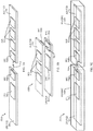
- FIG. 4A is a diagram illustrating an example embodiment of springs 401 that may be located within the housing 400 of the head worn computer. In FIG. 4A , the springs401 are shown removed from the regions of the housing that contain the springs 401.
- FIG. 4B is a diagram illustrating an example embodiment of springs 401 in isolation. In FIG. 4B , the springs 401 are shown removed from the housing entirely.
- FIG. 5 is an illustration of an example embodiment of the head worn computer worn on the head of a user.
- the housing 500 rests on the back of the user's head and remains stationary.
- End region 503 rests above the user's ear, close to the temple at the front of the user's head.
- the end region includes a mount 504.
- a display 501 may be attached to the mount 504.
- the display 501 can be positioned directly in front of the user's eye 502.
- FIGs. 6A and 6B are block diagrams 600 and 611 of electrical circuits employing near field communication to transfer data between electronics modules of a head worn computer.
- NFC Near field communications
- smartphones and similar devices currently employ NFC technology.
- Present applications include contactless transactions, data exchange, and simplified setup of more complex communications, such as Wi-Fi.
- Communication is also possible between an NFC device and an unpowered NFC chip, called a "tag”.
- NFC technology e.g., 375Mb/sec.
- NFC technology can be used for convenience in mobile devices; consumers find such high speed downloads or data transfer rates useful for transferring files, particularly for large files, such as movies.
- the Toshiba Transfer Jet is a NFC technology that provides wireless near-field high speed data transfer, can operate up to a distance of 3.5 centimeters, and has a near-field radiated power dissipation level that is similar to very low power near-field Bluetooth power levels.
- the Transfer Jet is available from Toshiba America Electronic Components, Inc., 19900 MacArthur Boulevard, Suite 400, Irvine, California.
- NFC modules can be employed as an interface to provide near-field high speed wireless data transfer to interface between electronics modules or printed circuit boards (PCBs) (also referred to herein as printed circuit board assemblies (PCBAs)).
- PCBs are used to mechanically support and electrically connect electronic components using conductive pathways, tracks, or signal traces etched from copper sheets laminated onto a non-conductive substrate.
- Multiple PCBs are typically interconnected using large multi-wire busses or, sometimes, vias are used for "stacked" configurations or for multi-layer boards.
- the PCBs of the head worn computers can be equipped with NFC modules.
- the NFC modules can replace the large multi-wire busses and vias used to interface between multiple PCBs.
- the NFC module equipped PCBs can be arranged in a stacked configuration (e.g., the PCB connected in a parallel configuration) or placed end-to-end (e.g., the PCBs connected in a series configuration).
- NFC modules allow the PCBAs to be placed in a thinner or lower profile stack because the volume needed to fit large multi-pin PCBA to PCBA connectors is no longer required.
- a first NFC module is located within a NFC range of a second NFC module to enable an interfacing wireless communications link between the two NFC modules.
- An example NFC range such as the Transfer Jet, is up to 3.5 centimeters, although the data transmit and reception range can be controlled by system software. Control of operating NFC ranges may be based on particular use and application to optimize a feature of system performance, such as transfer rate or battery life.
- NFC module when the NFC module is used for high speed data transfer between the head worn computer and another device, such as a Smartphone or another head worn computer, application software (or operating system instructions) can select a single or multiple NFC modules as the data transfer point to interface with the other device.
- PCBAs can be sealed to the outside having only a power and/or ground external connection.
- the PCBAs can be more easily hermetically sealed, because there are large number of external connection points of the multi-wire busses and vias have been eliminated.
- higher levels of system reliability and system life-span are possible because exposure to dust and moisture are greatly reduced.
- NFC modules allow the PCBAs to move or flex within the physical constraints of a system architecture or industrial design free from the possibility of physical damage associated with the multi-wire busses, flex circuit interfaces, or connectors becoming loose or making intermittent contact during vibration or other PCBA to PCBA movement.
- Using near field wireless high speed data transfer technology can eliminate large multiple pin connectors on two or more adjoining PCBAs, as well as any high speed multiple wire data bus or flex circuit interfaces. Eliminating the sharp right angle connection of PCBAs to PCBAs and the speed multi-wire bus or cables from PCBA to PCBA can improve and lower high speed system EMI and regional RF emission certifications.
- PCBs equipped with NFC modules may allow head worn computers to employ hinges, system housing flex points, and flexible or stiff regions in its industrial design and be freed from the problems of passing large multi-wire busses or flex circuits interfaces through or about the hinges or flex points.
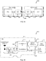
- FIG 6A is block diagram of circuit 600, an example embedment of PCBs equipped with NFC modules arranged to be within the near field range of each other and configured to establish a communications link.
- the circuit 600 includes a central processing unit printed circuit board assembly 601 (CPU PCB) and an auxiliary printed circuit board assembly 611 (AUX PCB).
- CPU PCB 601 includes a central processing unit 603 (CPU) communicatively coupled 615 to an NFC module 605.
- the CPU 603 can be, for example, an OMAP4430 multimedia application processor available from Texas Instruments Inc., 12500 TI Boulevard Dallas, Texas.
- the CPU PCB 603 can include any or more of these details.
- the AUX PCB 611 includes an auxiliary module 603 (AUX) communicatively coupled 615 to an NFC module 605.
- AUX auxiliary module
- NFC modules 605 are arranged in close proximity, that is, within an operable near field range of one another.
- the NFC modules are configured to establish a bi-directional wireless communications link 650.
- a bi-directional wireless communications link 650 can be established using any appropriate NFC protocol and/or data exchange format.
- the AUX PCB 611 can include multiple AUXs 613, such as an audio codec and mini-DSP module, head tracker module, micro-SD card, power regulators, GPS receivers, wireless communications modules employing protocols such as Wi-Fi, Bluetooth, etc., eMMC embedded storage.
- the AUX PCB 611 can not only include additional AUXs 613, such as those listed above, but also include communications pathways, such as traces, wires, etc. that enable operable coupling.
- FIG. 6B is a schematic diagram of the AUX PCB 611 showing more details of the NFC module 605.
- the AUX PCB 611 includes the AUX module 613, operable coupling 615, and NFC module 605.
- the NFC module 605 can include NFC integrated circuit (NFC IC) 655 and radio frequency (RF) circuit 660.
- NFC IC NFC integrated circuit
- RF radio frequency
- FIGs. 7A - 7C are block diagrams illustrating example arrangements of PCBs equipped with NFC modules.
- FIG. 7A is a block diagram illustrating an example embodiment of a series arrangement 700a (also referred to as end-to-end) of PCBs including CPU PCB 701 and AUX PCB 711.
- the CPU PCB 701 includes the CPU 703 and NFC module 705a.
- the AUX PCB 711 includes multiple AUXs 713 and NFC module 705b.
- the NFC modules 705a-b are arranged to be positioned at an end of their respective PCBs. In other words, a first NFC module 705a is located at an end, near the edge of the CPU PCB 701 and a second NFC module 705b is located at an end, near an edge of the AUX PCB 711.
- the CPU PCB 701 and AUX PCB 711 are arranged such that the location of each respective NFC module 705a-b is located within the near field range of its respective communications link partner to enable the wireless transfer of data through communications link 750.
- FIG. 7B is a block diagram illustrating an example embodiment of a parallel arrangement 700b (also referred to as stacked) of PCBs including CPU PCB 701 and AUX PCB 711. Similar to FIG. 7A , the CPU PCB 701 includes the CPU 703 and NFC module 705a, and the AUX PCB 711 includes multiple AUXs 713 and NFC module 705b. Unlike the series arrangement 700a, the in parallel arrangement 700b the NFC 705b of AUX PCB 711 is mounted on the underside so as to enable the NFC modules 705a-b to be located within the near field range of each other.
- FIG. 7C is a block diagram illustrating an example embodiment of a series arrangement 700c of PCBs, including CPU PCB 701 and AUX PCB 711, that is similar to series arrangement 700a but for the CPU PCB 701 and AUX PCB 711 each being encased in a housing 760a-b, respectively.
- the housings 760a-b should be designed to enable the NFC modules 705a-b to be located within the near field range of each other in at least one operational position.
Landscapes
- Physics & Mathematics (AREA)
- Engineering & Computer Science (AREA)
- General Physics & Mathematics (AREA)
- Optics & Photonics (AREA)
- Computer Hardware Design (AREA)
- Theoretical Computer Science (AREA)
- Human Computer Interaction (AREA)
- General Engineering & Computer Science (AREA)
- Casings For Electric Apparatus (AREA)
- Telephone Set Structure (AREA)
- User Interface Of Digital Computer (AREA)
- Respiratory Apparatuses And Protective Means (AREA)
Applications Claiming Priority (3)
| Application Number | Priority Date | Filing Date | Title |
|---|---|---|---|
| US201261733391P | 2012-12-04 | 2012-12-04 | |
| US201361750266P | 2013-01-08 | 2013-01-08 | |
| PCT/US2013/072867 WO2014089074A2 (en) | 2012-12-04 | 2013-12-03 | Spring-loaded supports for head set computer |
Publications (2)
| Publication Number | Publication Date |
|---|---|
| EP2929405A2 EP2929405A2 (en) | 2015-10-14 |
| EP2929405B1 true EP2929405B1 (en) | 2019-11-06 |
Family
ID=49880998
Family Applications (1)
| Application Number | Title | Priority Date | Filing Date |
|---|---|---|---|
| EP13812293.2A Active EP2929405B1 (en) | 2012-12-04 | 2013-12-03 | Spring-loaded supports for head set computer |
Country Status (4)
| Country | Link |
|---|---|
| EP (1) | EP2929405B1 (enExample) |
| JP (1) | JP6244370B2 (enExample) |
| CN (1) | CN104854532B (enExample) |
| WO (1) | WO2014089074A2 (enExample) |
Families Citing this family (4)
| Publication number | Priority date | Publication date | Assignee | Title |
|---|---|---|---|---|
| CN106959572A (zh) * | 2016-02-17 | 2017-07-18 | 杭州美盛红外光电技术有限公司 | 一种带外接口的显示装置 |
| TWI652023B (zh) * | 2018-01-11 | 2019-03-01 | 廣達電腦股份有限公司 | 頭戴式顯示裝置 |
| US11506905B2 (en) * | 2019-06-21 | 2022-11-22 | Realwear, Inc. | Hinged head-mounted display |
| US11431038B2 (en) * | 2019-06-21 | 2022-08-30 | Realwear, Inc. | Battery system for a head-mounted display |
Citations (6)
| Publication number | Priority date | Publication date | Assignee | Title |
|---|---|---|---|---|
| EP0531645A2 (en) * | 1991-09-09 | 1993-03-17 | Psc, Inc. | Portable transaction terminal |
| JPH0622246A (ja) * | 1992-06-30 | 1994-01-28 | Sony Corp | 映像音声再生装置 |
| WO1995011473A1 (en) * | 1993-10-22 | 1995-04-27 | Kopin Corporation | Head-mounted display system |
| US20010047693A1 (en) * | 1998-08-17 | 2001-12-06 | Brian Klock | Mounting mechanism and head mounted apparatus |
| US6771424B1 (en) * | 1999-08-31 | 2004-08-03 | Shimadzu Corporation | Head-mounted display device |
| JP2009111512A (ja) * | 2007-10-26 | 2009-05-21 | Canon Inc | 頭部装着型機器 |
Family Cites Families (8)
| Publication number | Priority date | Publication date | Assignee | Title |
|---|---|---|---|---|
| US7310072B2 (en) * | 1993-10-22 | 2007-12-18 | Kopin Corporation | Portable communication display device |
| JP2004120153A (ja) * | 2002-09-25 | 2004-04-15 | Mitsubishi Electric Corp | 画像表示装置 |
| WO2004061519A1 (ja) * | 2002-12-24 | 2004-07-22 | Nikon Corporation | ヘッドマウントディスプレイ |
| WO2007129443A1 (ja) * | 2006-04-26 | 2007-11-15 | Nikon Corporation | ウエアラブルディスプレイ |
| WO2008088691A2 (en) * | 2007-01-12 | 2008-07-24 | Kopin Corporation | Head mounted monocular display device |
| US8520860B2 (en) * | 2007-12-13 | 2013-08-27 | Symbol Technologies, Inc. | Modular mobile computing headset |
| US9503555B2 (en) * | 2009-10-21 | 2016-11-22 | Symbol Technologies, Llc | Mounting device couplable to a human head |
| US20110090135A1 (en) * | 2009-10-21 | 2011-04-21 | Symbol Technologies, Inc. | Interchangeable display device for a head-mounted display system |
-
2013
- 2013-12-03 JP JP2015545513A patent/JP6244370B2/ja active Active
- 2013-12-03 WO PCT/US2013/072867 patent/WO2014089074A2/en not_active Ceased
- 2013-12-03 EP EP13812293.2A patent/EP2929405B1/en active Active
- 2013-12-03 CN CN201380063324.3A patent/CN104854532B/zh active Active
Patent Citations (6)
| Publication number | Priority date | Publication date | Assignee | Title |
|---|---|---|---|---|
| EP0531645A2 (en) * | 1991-09-09 | 1993-03-17 | Psc, Inc. | Portable transaction terminal |
| JPH0622246A (ja) * | 1992-06-30 | 1994-01-28 | Sony Corp | 映像音声再生装置 |
| WO1995011473A1 (en) * | 1993-10-22 | 1995-04-27 | Kopin Corporation | Head-mounted display system |
| US20010047693A1 (en) * | 1998-08-17 | 2001-12-06 | Brian Klock | Mounting mechanism and head mounted apparatus |
| US6771424B1 (en) * | 1999-08-31 | 2004-08-03 | Shimadzu Corporation | Head-mounted display device |
| JP2009111512A (ja) * | 2007-10-26 | 2009-05-21 | Canon Inc | 頭部装着型機器 |
Also Published As
| Publication number | Publication date |
|---|---|
| WO2014089074A2 (en) | 2014-06-12 |
| JP6244370B2 (ja) | 2017-12-06 |
| CN104854532A (zh) | 2015-08-19 |
| WO2014089074A3 (en) | 2014-10-30 |
| JP2016506563A (ja) | 2016-03-03 |
| EP2929405A2 (en) | 2015-10-14 |
| CN104854532B (zh) | 2018-10-19 |
Similar Documents
| Publication | Publication Date | Title |
|---|---|---|
| US9740239B2 (en) | Spring-loaded supports for head set computer | |
| US9874936B2 (en) | Wearable electronic device | |
| US8593374B2 (en) | Output device and wearable display | |
| JP2019054245A (ja) | インタポーザを含む電子装置 | |
| EP2929405B1 (en) | Spring-loaded supports for head set computer | |
| CN103972637A (zh) | 用于便携式终端的天线设备 | |
| KR101691797B1 (ko) | 이동 단말기 | |
| CN111866334B (zh) | 配备有柔性板的电子设备 | |
| JP6210614B2 (ja) | 無線通信機 | |
| KR101993374B1 (ko) | 휴대용 단말기의 전자 부품 접속 장치 | |
| US20140185858A1 (en) | Loudspeaker | |
| US20200084887A1 (en) | Flexible printed circuits for usb 3.0 interconnects in mobile devices | |
| KR20180095371A (ko) | 이동 단말기 및 인쇄 회로 기판 | |
| EP3082330A1 (en) | Mainboard structure and terminal | |
| KR20190042363A (ko) | 이동 단말기 | |
| KR100897416B1 (ko) | 이동통신 단말기 | |
| EP4398069A1 (en) | Modular strap for an electronic device | |
| JP5937138B2 (ja) | 眼鏡型電子機器 | |
| WO2018123668A1 (ja) | 電子機器 | |
| KR20220017182A (ko) | 전자파 차폐를 위한 구조를 갖는 fpcb 및 이를 포함하는 전자 장치 | |
| KR20160021516A (ko) | 전자 장치 | |
| CN101471501A (zh) | 电子设备 | |
| JP2008078480A (ja) | 電子機器 | |
| CN104883817A (zh) | 模块器件和具有模块器件的电子设备 | |
| JP2010129377A (ja) | コネクタ保護 |
Legal Events
| Date | Code | Title | Description |
|---|---|---|---|
| PUAI | Public reference made under article 153(3) epc to a published international application that has entered the european phase |
Free format text: ORIGINAL CODE: 0009012 |
|
| 17P | Request for examination filed |
Effective date: 20150429 |
|
| AK | Designated contracting states |
Kind code of ref document: A2 Designated state(s): AL AT BE BG CH CY CZ DE DK EE ES FI FR GB GR HR HU IE IS IT LI LT LU LV MC MK MT NL NO PL PT RO RS SE SI SK SM TR |
|
| AX | Request for extension of the european patent |
Extension state: BA ME |
|
| DAX | Request for extension of the european patent (deleted) | ||
| PUAG | Search results despatched under rule 164(2) epc together with communication from examining division |
Free format text: ORIGINAL CODE: 0009017 |
|
| STAA | Information on the status of an ep patent application or granted ep patent |
Free format text: STATUS: EXAMINATION IS IN PROGRESS |
|
| 17Q | First examination report despatched |
Effective date: 20180612 |
|
| B565 | Issuance of search results under rule 164(2) epc |
Effective date: 20180612 |
|
| RIC1 | Information provided on ipc code assigned before grant |
Ipc: G06F 1/16 20060101AFI20180607BHEP Ipc: G02B 27/01 20060101ALI20180607BHEP Ipc: H04M 1/05 20060101ALI20180607BHEP |
|
| GRAP | Despatch of communication of intention to grant a patent |
Free format text: ORIGINAL CODE: EPIDOSNIGR1 |
|
| STAA | Information on the status of an ep patent application or granted ep patent |
Free format text: STATUS: GRANT OF PATENT IS INTENDED |
|
| INTG | Intention to grant announced |
Effective date: 20190813 |
|
| GRAS | Grant fee paid |
Free format text: ORIGINAL CODE: EPIDOSNIGR3 |
|
| GRAA | (expected) grant |
Free format text: ORIGINAL CODE: 0009210 |
|
| STAA | Information on the status of an ep patent application or granted ep patent |
Free format text: STATUS: THE PATENT HAS BEEN GRANTED |
|
| AK | Designated contracting states |
Kind code of ref document: B1 Designated state(s): AL AT BE BG CH CY CZ DE DK EE ES FI FR GB GR HR HU IE IS IT LI LT LU LV MC MK MT NL NO PL PT RO RS SE SI SK SM TR |
|
| REG | Reference to a national code |
Ref country code: GB Ref legal event code: FG4D |
|
| REG | Reference to a national code |
Ref country code: CH Ref legal event code: EP Ref country code: AT Ref legal event code: REF Ref document number: 1199637 Country of ref document: AT Kind code of ref document: T Effective date: 20191115 |
|
| REG | Reference to a national code |
Ref country code: IE Ref legal event code: FG4D |
|
| REG | Reference to a national code |
Ref country code: DE Ref legal event code: R096 Ref document number: 602013062632 Country of ref document: DE |
|
| REG | Reference to a national code |
Ref country code: NL Ref legal event code: MP Effective date: 20191106 |
|
| REG | Reference to a national code |
Ref country code: LT Ref legal event code: MG4D |
|
| PG25 | Lapsed in a contracting state [announced via postgrant information from national office to epo] |
Ref country code: FI Free format text: LAPSE BECAUSE OF FAILURE TO SUBMIT A TRANSLATION OF THE DESCRIPTION OR TO PAY THE FEE WITHIN THE PRESCRIBED TIME-LIMIT Effective date: 20191106 Ref country code: GR Free format text: LAPSE BECAUSE OF FAILURE TO SUBMIT A TRANSLATION OF THE DESCRIPTION OR TO PAY THE FEE WITHIN THE PRESCRIBED TIME-LIMIT Effective date: 20200207 Ref country code: PL Free format text: LAPSE BECAUSE OF FAILURE TO SUBMIT A TRANSLATION OF THE DESCRIPTION OR TO PAY THE FEE WITHIN THE PRESCRIBED TIME-LIMIT Effective date: 20191106 Ref country code: NO Free format text: LAPSE BECAUSE OF FAILURE TO SUBMIT A TRANSLATION OF THE DESCRIPTION OR TO PAY THE FEE WITHIN THE PRESCRIBED TIME-LIMIT Effective date: 20200206 Ref country code: LT Free format text: LAPSE BECAUSE OF FAILURE TO SUBMIT A TRANSLATION OF THE DESCRIPTION OR TO PAY THE FEE WITHIN THE PRESCRIBED TIME-LIMIT Effective date: 20191106 Ref country code: NL Free format text: LAPSE BECAUSE OF FAILURE TO SUBMIT A TRANSLATION OF THE DESCRIPTION OR TO PAY THE FEE WITHIN THE PRESCRIBED TIME-LIMIT Effective date: 20191106 Ref country code: PT Free format text: LAPSE BECAUSE OF FAILURE TO SUBMIT A TRANSLATION OF THE DESCRIPTION OR TO PAY THE FEE WITHIN THE PRESCRIBED TIME-LIMIT Effective date: 20200306 Ref country code: LV Free format text: LAPSE BECAUSE OF FAILURE TO SUBMIT A TRANSLATION OF THE DESCRIPTION OR TO PAY THE FEE WITHIN THE PRESCRIBED TIME-LIMIT Effective date: 20191106 Ref country code: SE Free format text: LAPSE BECAUSE OF FAILURE TO SUBMIT A TRANSLATION OF THE DESCRIPTION OR TO PAY THE FEE WITHIN THE PRESCRIBED TIME-LIMIT Effective date: 20191106 Ref country code: BG Free format text: LAPSE BECAUSE OF FAILURE TO SUBMIT A TRANSLATION OF THE DESCRIPTION OR TO PAY THE FEE WITHIN THE PRESCRIBED TIME-LIMIT Effective date: 20200206 |
|
| PG25 | Lapsed in a contracting state [announced via postgrant information from national office to epo] |
Ref country code: IS Free format text: LAPSE BECAUSE OF FAILURE TO SUBMIT A TRANSLATION OF THE DESCRIPTION OR TO PAY THE FEE WITHIN THE PRESCRIBED TIME-LIMIT Effective date: 20200306 Ref country code: RS Free format text: LAPSE BECAUSE OF FAILURE TO SUBMIT A TRANSLATION OF THE DESCRIPTION OR TO PAY THE FEE WITHIN THE PRESCRIBED TIME-LIMIT Effective date: 20191106 Ref country code: HR Free format text: LAPSE BECAUSE OF FAILURE TO SUBMIT A TRANSLATION OF THE DESCRIPTION OR TO PAY THE FEE WITHIN THE PRESCRIBED TIME-LIMIT Effective date: 20191106 |
|
| PG25 | Lapsed in a contracting state [announced via postgrant information from national office to epo] |
Ref country code: AL Free format text: LAPSE BECAUSE OF FAILURE TO SUBMIT A TRANSLATION OF THE DESCRIPTION OR TO PAY THE FEE WITHIN THE PRESCRIBED TIME-LIMIT Effective date: 20191106 |
|
| PG25 | Lapsed in a contracting state [announced via postgrant information from national office to epo] |
Ref country code: ES Free format text: LAPSE BECAUSE OF FAILURE TO SUBMIT A TRANSLATION OF THE DESCRIPTION OR TO PAY THE FEE WITHIN THE PRESCRIBED TIME-LIMIT Effective date: 20191106 Ref country code: DK Free format text: LAPSE BECAUSE OF FAILURE TO SUBMIT A TRANSLATION OF THE DESCRIPTION OR TO PAY THE FEE WITHIN THE PRESCRIBED TIME-LIMIT Effective date: 20191106 Ref country code: RO Free format text: LAPSE BECAUSE OF FAILURE TO SUBMIT A TRANSLATION OF THE DESCRIPTION OR TO PAY THE FEE WITHIN THE PRESCRIBED TIME-LIMIT Effective date: 20191106 Ref country code: CZ Free format text: LAPSE BECAUSE OF FAILURE TO SUBMIT A TRANSLATION OF THE DESCRIPTION OR TO PAY THE FEE WITHIN THE PRESCRIBED TIME-LIMIT Effective date: 20191106 Ref country code: EE Free format text: LAPSE BECAUSE OF FAILURE TO SUBMIT A TRANSLATION OF THE DESCRIPTION OR TO PAY THE FEE WITHIN THE PRESCRIBED TIME-LIMIT Effective date: 20191106 |
|
| REG | Reference to a national code |
Ref country code: CH Ref legal event code: PL |
|
| REG | Reference to a national code |
Ref country code: DE Ref legal event code: R097 Ref document number: 602013062632 Country of ref document: DE |
|
| REG | Reference to a national code |
Ref country code: AT Ref legal event code: MK05 Ref document number: 1199637 Country of ref document: AT Kind code of ref document: T Effective date: 20191106 |
|
| REG | Reference to a national code |
Ref country code: BE Ref legal event code: MM Effective date: 20191231 |
|
| PG25 | Lapsed in a contracting state [announced via postgrant information from national office to epo] |
Ref country code: MC Free format text: LAPSE BECAUSE OF FAILURE TO SUBMIT A TRANSLATION OF THE DESCRIPTION OR TO PAY THE FEE WITHIN THE PRESCRIBED TIME-LIMIT Effective date: 20191106 Ref country code: SK Free format text: LAPSE BECAUSE OF FAILURE TO SUBMIT A TRANSLATION OF THE DESCRIPTION OR TO PAY THE FEE WITHIN THE PRESCRIBED TIME-LIMIT Effective date: 20191106 Ref country code: SM Free format text: LAPSE BECAUSE OF FAILURE TO SUBMIT A TRANSLATION OF THE DESCRIPTION OR TO PAY THE FEE WITHIN THE PRESCRIBED TIME-LIMIT Effective date: 20191106 |
|
| PLBE | No opposition filed within time limit |
Free format text: ORIGINAL CODE: 0009261 |
|
| STAA | Information on the status of an ep patent application or granted ep patent |
Free format text: STATUS: NO OPPOSITION FILED WITHIN TIME LIMIT |
|
| 26N | No opposition filed |
Effective date: 20200807 |
|
| PG25 | Lapsed in a contracting state [announced via postgrant information from national office to epo] |
Ref country code: LU Free format text: LAPSE BECAUSE OF NON-PAYMENT OF DUE FEES Effective date: 20191203 Ref country code: IE Free format text: LAPSE BECAUSE OF NON-PAYMENT OF DUE FEES Effective date: 20191203 |
|
| PG25 | Lapsed in a contracting state [announced via postgrant information from national office to epo] |
Ref country code: BE Free format text: LAPSE BECAUSE OF NON-PAYMENT OF DUE FEES Effective date: 20191231 Ref country code: CH Free format text: LAPSE BECAUSE OF NON-PAYMENT OF DUE FEES Effective date: 20191231 Ref country code: LI Free format text: LAPSE BECAUSE OF NON-PAYMENT OF DUE FEES Effective date: 20191231 Ref country code: SI Free format text: LAPSE BECAUSE OF FAILURE TO SUBMIT A TRANSLATION OF THE DESCRIPTION OR TO PAY THE FEE WITHIN THE PRESCRIBED TIME-LIMIT Effective date: 20191106 Ref country code: AT Free format text: LAPSE BECAUSE OF FAILURE TO SUBMIT A TRANSLATION OF THE DESCRIPTION OR TO PAY THE FEE WITHIN THE PRESCRIBED TIME-LIMIT Effective date: 20191106 |
|
| PG25 | Lapsed in a contracting state [announced via postgrant information from national office to epo] |
Ref country code: IT Free format text: LAPSE BECAUSE OF FAILURE TO SUBMIT A TRANSLATION OF THE DESCRIPTION OR TO PAY THE FEE WITHIN THE PRESCRIBED TIME-LIMIT Effective date: 20191106 |
|
| PG25 | Lapsed in a contracting state [announced via postgrant information from national office to epo] |
Ref country code: CY Free format text: LAPSE BECAUSE OF FAILURE TO SUBMIT A TRANSLATION OF THE DESCRIPTION OR TO PAY THE FEE WITHIN THE PRESCRIBED TIME-LIMIT Effective date: 20191106 |
|
| PG25 | Lapsed in a contracting state [announced via postgrant information from national office to epo] |
Ref country code: MT Free format text: LAPSE BECAUSE OF FAILURE TO SUBMIT A TRANSLATION OF THE DESCRIPTION OR TO PAY THE FEE WITHIN THE PRESCRIBED TIME-LIMIT Effective date: 20191106 Ref country code: HU Free format text: LAPSE BECAUSE OF FAILURE TO SUBMIT A TRANSLATION OF THE DESCRIPTION OR TO PAY THE FEE WITHIN THE PRESCRIBED TIME-LIMIT; INVALID AB INITIO Effective date: 20131203 |
|
| PG25 | Lapsed in a contracting state [announced via postgrant information from national office to epo] |
Ref country code: TR Free format text: LAPSE BECAUSE OF FAILURE TO SUBMIT A TRANSLATION OF THE DESCRIPTION OR TO PAY THE FEE WITHIN THE PRESCRIBED TIME-LIMIT Effective date: 20191106 |
|
| PG25 | Lapsed in a contracting state [announced via postgrant information from national office to epo] |
Ref country code: MK Free format text: LAPSE BECAUSE OF FAILURE TO SUBMIT A TRANSLATION OF THE DESCRIPTION OR TO PAY THE FEE WITHIN THE PRESCRIBED TIME-LIMIT Effective date: 20191106 |
|
| PGFP | Annual fee paid to national office [announced via postgrant information from national office to epo] |
Ref country code: GB Payment date: 20241001 Year of fee payment: 12 |
|
| PGFP | Annual fee paid to national office [announced via postgrant information from national office to epo] |
Ref country code: FR Payment date: 20241001 Year of fee payment: 12 |
|
| PGFP | Annual fee paid to national office [announced via postgrant information from national office to epo] |
Ref country code: DE Payment date: 20250930 Year of fee payment: 13 |