EP2929239B1 - Flat lighting device - Google Patents
Flat lighting device Download PDFInfo
- Publication number
- EP2929239B1 EP2929239B1 EP13818440.3A EP13818440A EP2929239B1 EP 2929239 B1 EP2929239 B1 EP 2929239B1 EP 13818440 A EP13818440 A EP 13818440A EP 2929239 B1 EP2929239 B1 EP 2929239B1
- Authority
- EP
- European Patent Office
- Prior art keywords
- carrier
- lighting device
- cover member
- light source
- solid state
- Prior art date
- Legal status (The legal status is an assumption and is not a legal conclusion. Google has not performed a legal analysis and makes no representation as to the accuracy of the status listed.)
- Active
Links
- 239000007787 solid Substances 0.000 claims description 46
- 239000000463 material Substances 0.000 claims description 35
- 239000004020 conductor Substances 0.000 claims description 13
- XAGFODPZIPBFFR-UHFFFAOYSA-N aluminium Chemical compound [Al] XAGFODPZIPBFFR-UHFFFAOYSA-N 0.000 claims description 10
- 229910052782 aluminium Inorganic materials 0.000 claims description 10
- RYGMFSIKBFXOCR-UHFFFAOYSA-N Copper Chemical compound [Cu] RYGMFSIKBFXOCR-UHFFFAOYSA-N 0.000 claims description 9
- 229910052802 copper Inorganic materials 0.000 claims description 9
- 239000010949 copper Substances 0.000 claims description 9
- 239000004411 aluminium Substances 0.000 claims description 6
- 239000000758 substrate Substances 0.000 claims 1
- 230000003287 optical effect Effects 0.000 description 30
- 238000009826 distribution Methods 0.000 description 16
- 238000003892 spreading Methods 0.000 description 15
- 230000007480 spreading Effects 0.000 description 15
- 229920003023 plastic Polymers 0.000 description 14
- 239000004033 plastic Substances 0.000 description 14
- 239000000969 carrier Substances 0.000 description 11
- 239000003570 air Substances 0.000 description 9
- 230000008901 benefit Effects 0.000 description 5
- 238000001816 cooling Methods 0.000 description 5
- 238000004519 manufacturing process Methods 0.000 description 4
- 229910052751 metal Inorganic materials 0.000 description 4
- 239000002184 metal Substances 0.000 description 4
- 230000001419 dependent effect Effects 0.000 description 3
- 239000011521 glass Substances 0.000 description 3
- 238000005304 joining Methods 0.000 description 3
- 230000005855 radiation Effects 0.000 description 3
- 238000004364 calculation method Methods 0.000 description 2
- 238000010276 construction Methods 0.000 description 2
- 230000007423 decrease Effects 0.000 description 2
- 230000000694 effects Effects 0.000 description 2
- 230000004907 flux Effects 0.000 description 2
- 230000001681 protective effect Effects 0.000 description 2
- 238000004088 simulation Methods 0.000 description 2
- 239000012780 transparent material Substances 0.000 description 2
- 238000003466 welding Methods 0.000 description 2
- 239000011188 CEM-1 Substances 0.000 description 1
- 101100257127 Caenorhabditis elegans sma-2 gene Proteins 0.000 description 1
- 238000004026 adhesive bonding Methods 0.000 description 1
- AZDRQVAHHNSJOQ-UHFFFAOYSA-N alumane Chemical group [AlH3] AZDRQVAHHNSJOQ-UHFFFAOYSA-N 0.000 description 1
- 239000012080 ambient air Substances 0.000 description 1
- 230000015572 biosynthetic process Effects 0.000 description 1
- 239000000919 ceramic Substances 0.000 description 1
- 229910010293 ceramic material Inorganic materials 0.000 description 1
- 239000011248 coating agent Substances 0.000 description 1
- 238000000576 coating method Methods 0.000 description 1
- 230000008878 coupling Effects 0.000 description 1
- 238000010168 coupling process Methods 0.000 description 1
- 238000005859 coupling reaction Methods 0.000 description 1
- 238000010292 electrical insulation Methods 0.000 description 1
- 229920006351 engineering plastic Polymers 0.000 description 1
- 238000005755 formation reaction Methods 0.000 description 1
- 239000003292 glue Substances 0.000 description 1
- 230000017525 heat dissipation Effects 0.000 description 1
- 238000012821 model calculation Methods 0.000 description 1
- 238000012986 modification Methods 0.000 description 1
- 230000004048 modification Effects 0.000 description 1
- 150000003071 polychlorinated biphenyls Chemical class 0.000 description 1
- 238000009420 retrofitting Methods 0.000 description 1
- 230000035939 shock Effects 0.000 description 1
Images


Classifications
-
- H—ELECTRICITY
- H05—ELECTRIC TECHNIQUES NOT OTHERWISE PROVIDED FOR
- H05K—PRINTED CIRCUITS; CASINGS OR CONSTRUCTIONAL DETAILS OF ELECTRIC APPARATUS; MANUFACTURE OF ASSEMBLAGES OF ELECTRICAL COMPONENTS
- H05K1/00—Printed circuits
- H05K1/02—Details
- H05K1/0201—Thermal arrangements, e.g. for cooling, heating or preventing overheating
- H05K1/0203—Cooling of mounted components
- H05K1/0209—External configuration of printed circuit board adapted for heat dissipation, e.g. lay-out of conductors, coatings
-
- F—MECHANICAL ENGINEERING; LIGHTING; HEATING; WEAPONS; BLASTING
- F21—LIGHTING
- F21V—FUNCTIONAL FEATURES OR DETAILS OF LIGHTING DEVICES OR SYSTEMS THEREOF; STRUCTURAL COMBINATIONS OF LIGHTING DEVICES WITH OTHER ARTICLES, NOT OTHERWISE PROVIDED FOR
- F21V5/00—Refractors for light sources
- F21V5/04—Refractors for light sources of lens shape
-
- F—MECHANICAL ENGINEERING; LIGHTING; HEATING; WEAPONS; BLASTING
- F21—LIGHTING
- F21K—NON-ELECTRIC LIGHT SOURCES USING LUMINESCENCE; LIGHT SOURCES USING ELECTROCHEMILUMINESCENCE; LIGHT SOURCES USING CHARGES OF COMBUSTIBLE MATERIAL; LIGHT SOURCES USING SEMICONDUCTOR DEVICES AS LIGHT-GENERATING ELEMENTS; LIGHT SOURCES NOT OTHERWISE PROVIDED FOR
- F21K9/00—Light sources using semiconductor devices as light-generating elements, e.g. using light-emitting diodes [LED] or lasers
- F21K9/60—Optical arrangements integrated in the light source, e.g. for improving the colour rendering index or the light extraction
- F21K9/61—Optical arrangements integrated in the light source, e.g. for improving the colour rendering index or the light extraction using light guides
-
- F—MECHANICAL ENGINEERING; LIGHTING; HEATING; WEAPONS; BLASTING
- F21—LIGHTING
- F21V—FUNCTIONAL FEATURES OR DETAILS OF LIGHTING DEVICES OR SYSTEMS THEREOF; STRUCTURAL COMBINATIONS OF LIGHTING DEVICES WITH OTHER ARTICLES, NOT OTHERWISE PROVIDED FOR
- F21V19/00—Fastening of light sources or lamp holders
- F21V19/001—Fastening of light sources or lamp holders the light sources being semiconductors devices, e.g. LEDs
- F21V19/003—Fastening of light source holders, e.g. of circuit boards or substrates holding light sources
-
- F—MECHANICAL ENGINEERING; LIGHTING; HEATING; WEAPONS; BLASTING
- F21—LIGHTING
- F21V—FUNCTIONAL FEATURES OR DETAILS OF LIGHTING DEVICES OR SYSTEMS THEREOF; STRUCTURAL COMBINATIONS OF LIGHTING DEVICES WITH OTHER ARTICLES, NOT OTHERWISE PROVIDED FOR
- F21V29/00—Protecting lighting devices from thermal damage; Cooling or heating arrangements specially adapted for lighting devices or systems
- F21V29/50—Cooling arrangements
- F21V29/502—Cooling arrangements characterised by the adaptation for cooling of specific components
- F21V29/503—Cooling arrangements characterised by the adaptation for cooling of specific components of light sources
-
- F—MECHANICAL ENGINEERING; LIGHTING; HEATING; WEAPONS; BLASTING
- F21—LIGHTING
- F21V—FUNCTIONAL FEATURES OR DETAILS OF LIGHTING DEVICES OR SYSTEMS THEREOF; STRUCTURAL COMBINATIONS OF LIGHTING DEVICES WITH OTHER ARTICLES, NOT OTHERWISE PROVIDED FOR
- F21V29/00—Protecting lighting devices from thermal damage; Cooling or heating arrangements specially adapted for lighting devices or systems
- F21V29/50—Cooling arrangements
- F21V29/502—Cooling arrangements characterised by the adaptation for cooling of specific components
- F21V29/506—Cooling arrangements characterised by the adaptation for cooling of specific components of globes, bowls or cover glasses
-
- F—MECHANICAL ENGINEERING; LIGHTING; HEATING; WEAPONS; BLASTING
- F21—LIGHTING
- F21V—FUNCTIONAL FEATURES OR DETAILS OF LIGHTING DEVICES OR SYSTEMS THEREOF; STRUCTURAL COMBINATIONS OF LIGHTING DEVICES WITH OTHER ARTICLES, NOT OTHERWISE PROVIDED FOR
- F21V29/00—Protecting lighting devices from thermal damage; Cooling or heating arrangements specially adapted for lighting devices or systems
- F21V29/50—Cooling arrangements
- F21V29/502—Cooling arrangements characterised by the adaptation for cooling of specific components
- F21V29/507—Cooling arrangements characterised by the adaptation for cooling of specific components of means for protecting lighting devices from damage, e.g. housings
-
- F—MECHANICAL ENGINEERING; LIGHTING; HEATING; WEAPONS; BLASTING
- F21—LIGHTING
- F21V—FUNCTIONAL FEATURES OR DETAILS OF LIGHTING DEVICES OR SYSTEMS THEREOF; STRUCTURAL COMBINATIONS OF LIGHTING DEVICES WITH OTHER ARTICLES, NOT OTHERWISE PROVIDED FOR
- F21V29/00—Protecting lighting devices from thermal damage; Cooling or heating arrangements specially adapted for lighting devices or systems
- F21V29/50—Cooling arrangements
- F21V29/70—Cooling arrangements characterised by passive heat-dissipating elements, e.g. heat-sinks
- F21V29/74—Cooling arrangements characterised by passive heat-dissipating elements, e.g. heat-sinks with fins or blades
-
- F—MECHANICAL ENGINEERING; LIGHTING; HEATING; WEAPONS; BLASTING
- F21—LIGHTING
- F21V—FUNCTIONAL FEATURES OR DETAILS OF LIGHTING DEVICES OR SYSTEMS THEREOF; STRUCTURAL COMBINATIONS OF LIGHTING DEVICES WITH OTHER ARTICLES, NOT OTHERWISE PROVIDED FOR
- F21V29/00—Protecting lighting devices from thermal damage; Cooling or heating arrangements specially adapted for lighting devices or systems
- F21V29/50—Cooling arrangements
- F21V29/70—Cooling arrangements characterised by passive heat-dissipating elements, e.g. heat-sinks
- F21V29/80—Cooling arrangements characterised by passive heat-dissipating elements, e.g. heat-sinks with pins or wires
-
- F—MECHANICAL ENGINEERING; LIGHTING; HEATING; WEAPONS; BLASTING
- F21—LIGHTING
- F21V—FUNCTIONAL FEATURES OR DETAILS OF LIGHTING DEVICES OR SYSTEMS THEREOF; STRUCTURAL COMBINATIONS OF LIGHTING DEVICES WITH OTHER ARTICLES, NOT OTHERWISE PROVIDED FOR
- F21V7/00—Reflectors for light sources
- F21V7/22—Reflectors for light sources characterised by materials, surface treatments or coatings, e.g. dichroic reflectors
- F21V7/24—Reflectors for light sources characterised by materials, surface treatments or coatings, e.g. dichroic reflectors characterised by the material
-
- F—MECHANICAL ENGINEERING; LIGHTING; HEATING; WEAPONS; BLASTING
- F21—LIGHTING
- F21V—FUNCTIONAL FEATURES OR DETAILS OF LIGHTING DEVICES OR SYSTEMS THEREOF; STRUCTURAL COMBINATIONS OF LIGHTING DEVICES WITH OTHER ARTICLES, NOT OTHERWISE PROVIDED FOR
- F21V7/00—Reflectors for light sources
- F21V7/22—Reflectors for light sources characterised by materials, surface treatments or coatings, e.g. dichroic reflectors
- F21V7/28—Reflectors for light sources characterised by materials, surface treatments or coatings, e.g. dichroic reflectors characterised by coatings
-
- H—ELECTRICITY
- H05—ELECTRIC TECHNIQUES NOT OTHERWISE PROVIDED FOR
- H05K—PRINTED CIRCUITS; CASINGS OR CONSTRUCTIONAL DETAILS OF ELECTRIC APPARATUS; MANUFACTURE OF ASSEMBLAGES OF ELECTRICAL COMPONENTS
- H05K1/00—Printed circuits
- H05K1/18—Printed circuits structurally associated with non-printed electric components
- H05K1/189—Printed circuits structurally associated with non-printed electric components characterised by the use of a flexible or folded printed circuit
-
- F—MECHANICAL ENGINEERING; LIGHTING; HEATING; WEAPONS; BLASTING
- F21—LIGHTING
- F21K—NON-ELECTRIC LIGHT SOURCES USING LUMINESCENCE; LIGHT SOURCES USING ELECTROCHEMILUMINESCENCE; LIGHT SOURCES USING CHARGES OF COMBUSTIBLE MATERIAL; LIGHT SOURCES USING SEMICONDUCTOR DEVICES AS LIGHT-GENERATING ELEMENTS; LIGHT SOURCES NOT OTHERWISE PROVIDED FOR
- F21K9/00—Light sources using semiconductor devices as light-generating elements, e.g. using light-emitting diodes [LED] or lasers
- F21K9/20—Light sources comprising attachment means
- F21K9/23—Retrofit light sources for lighting devices with a single fitting for each light source, e.g. for substitution of incandescent lamps with bayonet or threaded fittings
- F21K9/232—Retrofit light sources for lighting devices with a single fitting for each light source, e.g. for substitution of incandescent lamps with bayonet or threaded fittings specially adapted for generating an essentially omnidirectional light distribution, e.g. with a glass bulb
-
- F—MECHANICAL ENGINEERING; LIGHTING; HEATING; WEAPONS; BLASTING
- F21—LIGHTING
- F21K—NON-ELECTRIC LIGHT SOURCES USING LUMINESCENCE; LIGHT SOURCES USING ELECTROCHEMILUMINESCENCE; LIGHT SOURCES USING CHARGES OF COMBUSTIBLE MATERIAL; LIGHT SOURCES USING SEMICONDUCTOR DEVICES AS LIGHT-GENERATING ELEMENTS; LIGHT SOURCES NOT OTHERWISE PROVIDED FOR
- F21K9/00—Light sources using semiconductor devices as light-generating elements, e.g. using light-emitting diodes [LED] or lasers
- F21K9/20—Light sources comprising attachment means
- F21K9/23—Retrofit light sources for lighting devices with a single fitting for each light source, e.g. for substitution of incandescent lamps with bayonet or threaded fittings
- F21K9/238—Arrangement or mounting of circuit elements integrated in the light source
-
- F—MECHANICAL ENGINEERING; LIGHTING; HEATING; WEAPONS; BLASTING
- F21—LIGHTING
- F21K—NON-ELECTRIC LIGHT SOURCES USING LUMINESCENCE; LIGHT SOURCES USING ELECTROCHEMILUMINESCENCE; LIGHT SOURCES USING CHARGES OF COMBUSTIBLE MATERIAL; LIGHT SOURCES USING SEMICONDUCTOR DEVICES AS LIGHT-GENERATING ELEMENTS; LIGHT SOURCES NOT OTHERWISE PROVIDED FOR
- F21K9/00—Light sources using semiconductor devices as light-generating elements, e.g. using light-emitting diodes [LED] or lasers
- F21K9/60—Optical arrangements integrated in the light source, e.g. for improving the colour rendering index or the light extraction
- F21K9/69—Details of refractors forming part of the light source
-
- F—MECHANICAL ENGINEERING; LIGHTING; HEATING; WEAPONS; BLASTING
- F21—LIGHTING
- F21K—NON-ELECTRIC LIGHT SOURCES USING LUMINESCENCE; LIGHT SOURCES USING ELECTROCHEMILUMINESCENCE; LIGHT SOURCES USING CHARGES OF COMBUSTIBLE MATERIAL; LIGHT SOURCES USING SEMICONDUCTOR DEVICES AS LIGHT-GENERATING ELEMENTS; LIGHT SOURCES NOT OTHERWISE PROVIDED FOR
- F21K9/00—Light sources using semiconductor devices as light-generating elements, e.g. using light-emitting diodes [LED] or lasers
- F21K9/90—Methods of manufacture
-
- F—MECHANICAL ENGINEERING; LIGHTING; HEATING; WEAPONS; BLASTING
- F21—LIGHTING
- F21V—FUNCTIONAL FEATURES OR DETAILS OF LIGHTING DEVICES OR SYSTEMS THEREOF; STRUCTURAL COMBINATIONS OF LIGHTING DEVICES WITH OTHER ARTICLES, NOT OTHERWISE PROVIDED FOR
- F21V15/00—Protecting lighting devices from damage
- F21V15/01—Housings, e.g. material or assembling of housing parts
-
- F—MECHANICAL ENGINEERING; LIGHTING; HEATING; WEAPONS; BLASTING
- F21—LIGHTING
- F21V—FUNCTIONAL FEATURES OR DETAILS OF LIGHTING DEVICES OR SYSTEMS THEREOF; STRUCTURAL COMBINATIONS OF LIGHTING DEVICES WITH OTHER ARTICLES, NOT OTHERWISE PROVIDED FOR
- F21V19/00—Fastening of light sources or lamp holders
- F21V19/006—Fastening of light sources or lamp holders of point-like light sources, e.g. incandescent or halogen lamps, with screw-threaded or bayonet base
-
- F—MECHANICAL ENGINEERING; LIGHTING; HEATING; WEAPONS; BLASTING
- F21—LIGHTING
- F21V—FUNCTIONAL FEATURES OR DETAILS OF LIGHTING DEVICES OR SYSTEMS THEREOF; STRUCTURAL COMBINATIONS OF LIGHTING DEVICES WITH OTHER ARTICLES, NOT OTHERWISE PROVIDED FOR
- F21V23/00—Arrangement of electric circuit elements in or on lighting devices
- F21V23/003—Arrangement of electric circuit elements in or on lighting devices the elements being electronics drivers or controllers for operating the light source, e.g. for a LED array
-
- F—MECHANICAL ENGINEERING; LIGHTING; HEATING; WEAPONS; BLASTING
- F21—LIGHTING
- F21V—FUNCTIONAL FEATURES OR DETAILS OF LIGHTING DEVICES OR SYSTEMS THEREOF; STRUCTURAL COMBINATIONS OF LIGHTING DEVICES WITH OTHER ARTICLES, NOT OTHERWISE PROVIDED FOR
- F21V3/00—Globes; Bowls; Cover glasses
- F21V3/02—Globes; Bowls; Cover glasses characterised by the shape
-
- F—MECHANICAL ENGINEERING; LIGHTING; HEATING; WEAPONS; BLASTING
- F21—LIGHTING
- F21Y—INDEXING SCHEME ASSOCIATED WITH SUBCLASSES F21K, F21L, F21S and F21V, RELATING TO THE FORM OR THE KIND OF THE LIGHT SOURCES OR OF THE COLOUR OF THE LIGHT EMITTED
- F21Y2105/00—Planar light sources
- F21Y2105/10—Planar light sources comprising a two-dimensional array of point-like light-generating elements
-
- F—MECHANICAL ENGINEERING; LIGHTING; HEATING; WEAPONS; BLASTING
- F21—LIGHTING
- F21Y—INDEXING SCHEME ASSOCIATED WITH SUBCLASSES F21K, F21L, F21S and F21V, RELATING TO THE FORM OR THE KIND OF THE LIGHT SOURCES OR OF THE COLOUR OF THE LIGHT EMITTED
- F21Y2107/00—Light sources with three-dimensionally disposed light-generating elements
- F21Y2107/90—Light sources with three-dimensionally disposed light-generating elements on two opposite sides of supports or substrates
-
- F—MECHANICAL ENGINEERING; LIGHTING; HEATING; WEAPONS; BLASTING
- F21—LIGHTING
- F21Y—INDEXING SCHEME ASSOCIATED WITH SUBCLASSES F21K, F21L, F21S and F21V, RELATING TO THE FORM OR THE KIND OF THE LIGHT SOURCES OR OF THE COLOUR OF THE LIGHT EMITTED
- F21Y2115/00—Light-generating elements of semiconductor light sources
- F21Y2115/10—Light-emitting diodes [LED]
-
- H—ELECTRICITY
- H05—ELECTRIC TECHNIQUES NOT OTHERWISE PROVIDED FOR
- H05K—PRINTED CIRCUITS; CASINGS OR CONSTRUCTIONAL DETAILS OF ELECTRIC APPARATUS; MANUFACTURE OF ASSEMBLAGES OF ELECTRICAL COMPONENTS
- H05K2201/00—Indexing scheme relating to printed circuits covered by H05K1/00
- H05K2201/10—Details of components or other objects attached to or integrated in a printed circuit board
- H05K2201/10007—Types of components
- H05K2201/10106—Light emitting diode [LED]
Definitions
- the present invention relates to flat lighting device comprising solid state light sources, and more specifically to flat lamp.
- LED lamps comprise a printed circuit board with LEDs arranged onto it.
- the printed circuit board is arranged in a horizontal manner when arranging the LED lamp in a standing position, or, if defining a longitudinal axis of the LED lamp, arranged with an angle to the longitudinal axis.
- a plastic or glass bulb is arranged in front of the printed circuit board in a light exit direction in order to manipulate the emitted light from the LEDs, and to protect components inside the lamp.
- a number of components are arranged with the main purpose of spreading and transferring the heat generated by the LEDs. These may be a heat spreader, heat fins, a metal housing and a cap.
- Such LED lamp hence comprises a large number of components in order to perform all tasks of the lamp such as generating and distributing light, transferring heat, protect the electric connections and provide a fire enclosure.
- US 2007/0121326 discloses a lighting device with a cover member enclosing a carrier, wherein the cover member serves also as a heat dissipation element.
- DE 10 2011 006 749 discloses a lighting device with a carrier covered by an electrically isolating element to prevent electrical shocks to the user.
- US 2012/0069570 discloses a lighting device with a central carrier surrounded by a cover manufactured in two pieces.
- US 2010/0181885 discloses a lighting device with a carrier covered on its front and back surfaces by two heat sinks.
- a lighting device comprising all the technical features of claim 1. It is recognized by the present invention that the desired thermal properties of a lighting device can be achieved by having a short thermal path between the light source and the outside of the cover, where the heat is dissipated to the ambient. This is realized by a solid state light source disposed on a carrier to which the heat transmitted by the solid state light source is transferred. The thermal interface from the carrier to the cover member ensures a short thermal path to the outside of the lighting device.
- This improved thermal performance is preferably realized when the carrier comprises a thermally conductive material having a first coefficient of thermal conductivity and the cover having a second coefficient of thermal conductivivity, the first coefficient of thermal conductivity being larger than the second coefficient of thermal conductivity.
- the heat is largely and quickly transferred to the carrier in the vicinity of the solid state light source, after which it is transferred via the thermal interface to the cover member, and from the outside of the cover member to the ambient.
- the heat is radiated to the ambient in substantially the same direction of the light emission, meaning that the heat leaves the lighting device on the same side as the light..
- the first coefficient of thermal conductivity is in the range from 100-300 W/mK, preferably between 160 and 240 W/mK
- the second coefficient of thermal conductivity is in the range from 0.2-10 W/mK, preferably between 0.5 and 5 W/mK.
- the thermal conductive material is disposed as a thermal conductive layer on the carrier.
- This conductive layer may be a metal layer like e.g. copper, which also shows an excellent electrical conductivity. Therefore, it can be used for making the electrical connections of the solid state light sources to the driver part of a lighting device.
- the thermal performance can further be improved by a thermal interface material, TIM that is arranged to fill a space between the cover member and the carrier.
- the TIM may be sandwiched between the cover member and the printed circuit board.
- the TIM may be provided on either or both of the front side and back side of the printed circuit board.
- the TIM may fill irregularities in the surfaces of the printed circuit board and the cover member, i.e. filling air gaps at the interface between the two.
- the TIM has a higher thermal conductivity than air, and thereby increases the heat transfer between the printed circuit board and the cover member.
- this lighting device may further comprise a connection member having a fixed position relative to the carrier for mechanically and electrically connecting the lighting device to a socket.
- the carrier is having a relatively large front side compared with its edge side and the solid state light source is arranged on the front side of the carrier.
- the cover member has an outer surface being a portion of the outside of the lighting device and has an inner surface, opposite to the outer surface, that is in thermal contact with the front side of the carrier, such that the thermal interface is formed.
- the present invention is applied to make, for instance a lighting device that is suitable for replacing a conventional incandescant type of lamp, also referred to as a retrofit lamp.
- a second solid state light source arranged on a back side of the carrier being opposite to the front side, a second cover member disposed on the carrier, whereby the second light source is arranged between the carrier and a light-transmitting part of the second cover member, such that a thermal interface exists between the carrier and the second cover member, the second cover member having a second outer surface being a second portion of the outside of the lighting device and having a second inner surface being opposite to the second outer surface and being in thermal contact with the back side of the carrier, such that the second thermal interface is formed.
- the front side and the back side of the lighting device may be constructed in a similar way.
- a retrofit lamp can be obtained that emits light in both direction respective to the front side and back side.
- the thermal performance of these embodiments is ensured when at least 50%, preferably 90% of the front side of the carrier is in thermal contact with the inner surface of the cover member.
- the heat is dissipated by the solid state light sources and spread to the surroundings of the solid state light sources via the carrier; the larger the part of the carrier that is in thermal contact with the cover member, the better the heat transfer is from the carrier to the cover member.
- a lighting device comprising a planar carrier including a thermally conductive layer, at least one solid state light source arranged on a front side of the carrier, and an insulating cover member in thermal contact with said front side and a back side opposite said front side, and said cover member being adapted to transfer heat from said carrier out of the lighting device.
- the cover member comprises an optical structure arranged on the carrier in front of the at least one light source and adapted to direct the light emitted by the at least one solid state light source.
- Such lighting device may thereby provide an effective heat transfer from the printed circuit board and out of the arrangement with few parts and in a compact manner. Due to the thermal contact of the cover member with both sides of the printed circuit board, a majority of the heat generated by the light sources may be transferred by the cover member.
- the cover member may be in direct contact with the printed circuit board.
- the cover member may comprise an inner surface facing the printed circuit board. The inner surface may be in direct contact with the front and back side of the printed circuit board.
- the lighting device may further provide a cost efficient manufacturing process due the few parts.
- the an optical structure may be designed to direct the light from the light source through the cover member in a desired way.
- the light source and the printed circuit board may together provide the functions of converting power, generating light and spreading the heat generated.
- the cover member and lens may provide the functions of manipulating/directing the light from the light source, transferring the heat from the printed circuit board and providing electrical insulation and fire enclosure of the arrangement.
- the cover member may further have a protective purpose, protecting the printed circuit board and light source from external damage.
- the lighting device may be arranged in a cap for use in an electrical socket, or integrated in a luminaire.
- the printed circuit board may comprise two flat sides, the front side and the back side.
- the printed circuit board may further be planar.
- Light sources may be arranged on either one or both sides of the printed circuit board.
- the cover member may be arranged such that it is in thermal contact with both sides of the printed circuit board.
- the cover member may be arranged to be in thermal contact with a substantial part of the printed circuit board, such as at least half of the front side and back side of the printed circuit board.
- the cover member may be formed of a glass material, a plastic material, a ceramic material or the like.
- a normal plastic material for a cover member may provide sufficient thermal properties to provide a heat transfer function from the printed circuit board.
- the cover member may be made of a thermal plastic material.
- the printed circuit board may comprise a heat spreading layer for spreading the heat generated by the light sources over a large area of the printed circuit board.
- the heat spreading layer may for instance be a copper layer or an aluminum layer.
- the heat spreading layer may further be adapted to spread heat from the front side to the back side of the printed circuit board, and vice verse.
- the printed circuit board may comprise more than one heat spreading layer.
- the printed circuit board may comprise an aluminum sheet metal provided with electrical connections of FR-4 or CEM-1 material. The aluminum sheet metal may thereby form the heat spreading layer and electrical interconnections.
- the cover member is arranged to enclose the printed circuit board and the at least one solid state light source. Wherein the cover member encloses the printed circuit board, and is in contact with both the front side and the back side of the printed circuit board, the cover member may provide the required stiffness to the arrangement in order to hold the printed circuit board.
- the printed circuit board may then be made very thin, for instance as thin as 0.2 mm. Since the cover member encloses both front and back side of the printed circuit board, the printed circuit board will anyway be held in place. The printed circuit board thereby does not need to provide stability to the arrangement, but may be focused on heat spreading, holding the light source and providing electrical tracks to the light source.
- the cover member may be in thermal contact with a large part of the printed circuit board, such as at least ninety percent of an external surface of the printed circuit board.
- the cover member may further be in thermal contact with edge surfaces of the printed circuit board. The edge surfaces may together with the front side and back side form a total external surface of the printed circuit board. The heat transfer from the printed circuit board may thereby be improved.
- the cover member may have an inner side and an outer side, wherein the inner side is in contact with the printed circuit board and adapted to transfer heat from the inner side to the outer side.
- the cover member may in one embodiment be formed of a transparent material and the lens may be formed as an integrated part of the cover member.
- the cover member and the lens may be formed of the same material in one piece.
- the material of the cover member including the lens may thereby provide both the thermal properties for heat transfer and the optical properties of the lens, directing the light from the light source.
- the material may be transparent or translucent due to the optical properties.
- the cover member and lens may be molded in one common piece.
- the cover member may be formed of a thermally conductive material, and as a separate part from the an optical structure which is formed of a transparent or translucent material.
- the lens may be formed of a material different from the material of the cover member.
- the material of the cover member may be designed for providing good heat transfer properties, such as a material with low thermal resistivity.
- the cover member may be non-transparent.
- the different material of the lens may be designed for good optical performance in directing the light from the light source.
- the lens may however have some thermal conductivity, i.e. contribute to the heat transfer from the printed circuit board.
- An inner side surface of the lens which may be in contact with the printed circuit board, may be designed to maximize the heat transfer from the printed circuit board to the lens. Such inner side surface may be flat.
- the cover member comprises a first and a second cover part adapted to be attached to each other and to be in contact with the front side and the back side of the printed circuit board respectively.
- the cover member may be in two parts, thereby facilitating the manufacturing and the assembly of the lighting device.
- the two parts may comprise fastening means arranged to mate with each other in order to be fixed the two parts to each other.
- Such fastening means may be a snap coupling, glue, screws, ultrasonic welding or the like.
- the printed circuit board may be sandwiched between the two cover parts when assembled.
- the first cover part may thereby be in thermal contact with the front side of the printed circuit board, and the second cover part may be in thermal contact with the back side of the printed circuit board.
- the first cover part may comprise a protrusion adapted to extend through an opening in the printed circuit board to align the printed circuit board inside the cover member.
- the cover member may comprise a protrusion extending through an opening in the printed circuit board.
- the position of the printed circuit board relative to the cover member may thereby be fixed.
- the protrusion on the first cover part may be adapted to mate with corresponding means on the second cover part, thereby fixing the two parts to each other and sandwiching the printed circuit board in between.
- the at least one solid state light source may comprise a plurality of solid state light sources arranged with a distance to each other, or arranged in subgroups with a distance between each subgroup, and wherein the an optical structure may comprise a number of lenses equal to the number of separated solid state light sources or the number of separated subgroups of solid state light sources.
- a plurality of light sources may be arranged on the printed circuit board.
- the plurality of lenses may each be designed to direct light from one light source or a subgroup of light sources arranged together. By spreading the light sources or subgroups of light sources on the printed circuit board, the heat generated by the light sources may further be spread along the extension area of the printed circuit board.
- the total light output from the lighting device may be highly controllable.
- the lens for a specific light source or subgroup of light sources may be specially designed for that light source or subgroup, and may be different from another lens for another light source or subgroup.
- the light output may be directed in certain directions by each lens such that the total light output is optimized for a specific purpose.
- each light source or subgroup may be controlled by a driver or controller to provide a light output unique for that specific light source or subgroup.
- the lighting device may have a longitudinal axis and the printed circuit board may extend in a first plane in parallel with the longitudinal axis.
- the lighting device may further comprise a cap, and wherein the printed circuit board is arranged on said cap.
- the cap may be adapted to fit in an electrical socket.
- the arrangement of the printed circuit board in the cap, extending in a plane along the longitudinal axis may provide a lighting device with few parts.
- the longitudinal axis may extend through the center of the cap.
- the at least one light source arranged on the printed circuit board may thereby emit light in a main direction which is perpendicular to the longitudinal axis.
- the lens may however direct light in a plurality of directions, including a direction substantially in parallel with the longitudinal axis.
- the cover member which encloses the printed circuit board, thereby extends in the same plane as the printed circuit board, and also be arranged in said cap.
- the cover member, the an optical structure, and the cap may provide an entire outer surface of the lighting device, together enclosing the printed circuit board and the at least one light source.
- the printed circuit board may extend in a plane perpendicular to said longitudinal axis.
- the printed circuit board may thereby be arranged with light sources providing a spotlight arrangement.
- the cover member may be arranged to be in contact with both the front and back side of the printed circuit board in order to provide the same thermal properties as for a lighting device with a printed circuit board in parallel with the longitudinal axis.
- a first section of the cover member encloses the printed circuit board extending in said first plane, and wherein a second section of the cover member extends in a second plane with an angle to said first plane.
- a further extension of the cover member may improve the heat transfer capability of the cover member due to a larger surface exposed to the surroundings of the lighting device.
- the second section of the cover member may extend in parallel with the longitudinal axis. The two sections of the cover member may thereby form a cross shaped cross section when seen in direction of the longitudinal axis. Alternatively may the second plane be transverse to the longitudinal axis as well as the first plane.
- the second section of the cover member may improve the optical performance of the lighting device.
- the second plane may be in parallel with the longitudinal axis, and with an angle to the first plane.
- the cover member may comprise further additional sections, such as a third and a fourth section.
- the sections may form various formations. For instance three sections of the cover member may form a triangle shape.
- the printed circuit board may be a first printed circuit board, and wherein the lighting device further comprises a second printed circuit board enclosed by the second section of the cover member.
- the second printed circuit board may be arranged to extend in said second plane transversal to the first plane in which the first printed circuit board extends.
- the second printed circuit board may be provided with at least one solid state light source.
- the second section of the cover member may be provided with an optical structure corresponding to the light source on the second printed circuit board.
- the optical structure may be designed to provide non-symmetric optical properties.
- the optical structure may be designed to direct the light from the at least on solid state light source in a non-symmetrical manner, providing a non-rotational symmetry of the luminous intensity distribution. That is, a circular or dome shaped lens may provide a non-uniform light output along its light output directions.
- the arrangement comprises a plurality of light sources and a plurality of lenses
- the lenses may be non-symmetrically designed such that the overall light output from the arrangement is uniform or in an otherwise desired way.
- the non-symmetric lens may be designed to direct a minimum amount of light towards a neighboring lens.
- the lens may comprise an inner cavity, which inner cavity surrounds the light source(s) which the lens is arranged in front of.
- the inner cavity may be shaped in order to provide the non-symmetric luminous intensity distribution of the lens. Due to the shape of the inner cavity, the refraction of the light from the light source(s) reaching the lens may provide a desired luminous intensity distribution. Alternatively, the non-symmetry of the lens may be provided by the design of an outer surface of the lens.
- said printed circuit board may be a first printed circuit board with a first front and back side having at least one solid state light source arranged on the first front side
- the lighting device further may comprise a second printed circuit board with a second front and back side and having at least one solid state light source arranged on said second front side, and wherein said second printed circuit board is arranged in parallel with said first printed circuit board.
- a lighting device comprising two flat light source holding plates in the same cap may provide an arrangement with an improved thermal resistance. I.e. the thermal resistance of the cover member in thermal contact with both printed circuit boards may be lowered.
- the cover member may be in thermal contact with the front sides and back sides of both printed circuit boards.
- the cover member may enclose both the first and the second printed circuit boards.
- Each front side of the printed circuit boards may be provided with one or more light sources.
- the two front sides may be directed in opposite directions. Heat from the light sources on the front sides may be spread also to the respective back side, thereby increasing the thermal performance of the arrangement.
- the printed circuit board may be formed as an integrated part of the cover member.
- the printed circuit board may be a part of an inner surface of the cover member.
- the electrical connections of the printed circuit board may be printed directly on said inner surface of the cover member, and the light sources may be arranged on said inner surface.
- the printed circuit board and the cover member may have a curved shape.
- the printed circuit board may extend in a bent or curved plane which has a radius.
- the cover member may have a corresponding shape and be in thermal contact with the front and back side of the curved printed circuit board.
- a flexible board material may be used for forming the printed circuit board. Such formed lighting device may in some embodiments provide improved optical performance of the arrangement.
- the printed circuit board may be a first printed circuit board and the lighting device may further comprise a second and a third printed circuit board, wherein the three printed circuit boards may be arranged with angles relative each other, and wherein the cover member may be in thermal contact with a front side and a back side of all printed circuit boards.
- An arrangement with the thermal properties and compact arrangement of the present invention may thereby be used in an embodiment with improved optical performance.
- the three printed circuit boards may be arranged, each with a longitudinal edge in contact with corresponding edges of the other printed circuit boards. Such longitudinal edge may coincide with a longitudinal axis of the lighting device.
- the printed circuit board may form a star like shape of the lighting device.
- the lighting device may also comprise further printed circuit boards forming other shapes and providing other optical performance, which may be desired in certain applications.
- the printed circuit board may have a buckled surface forming two printed circuit board sections extending with an angle to each other.
- buckled means that the two carrier sections are coupled to each other in such a way that the two carrier sections may be directed slightly differently, forming an angular bent shape of the carrier.
- Both carrier sections may be provided with light sources which thereby may emit light in different directions.
- the two carrier sections may be arranged in parallel with a longitudinal axis of the lighting device, but with an angle relative to each other. Alternatively, both sections may be arranged in parallel with an axis perpendicular to the longitudinal axis.
- the carrier is a double-helical shaped surface positioned in parallel to the longitudinal axis.
- This shape has the advantage that the solid state light sources that are connected to the carrier are now directed in other directions than only perpendicular to the longitudinal axis.
- the double-helical shaped surface has the property that a normal to this surface is in general not perpendicular to the longitudinal axis of the lighting device. This will lead to a lighting device having a more uniform luminous intensity distribution.
- the double-helical surface has a first end pointing in the direction of the connection member, and a second end pointing away from said connection member, wherein the respective orientations of double-helical surface perpendicular to the longitudinal axis at the first end and at the second end differ by an angle in the range from 15° - 360°.
- a uniform light distibution may be realized when the respective orientations differ by about 90°, even a difference in orientation of about 45° may give an acceptable performance.
- the lighting device may comprise electical connections for independently powering the solid state light source and the second solid state light source.
- This has the advantage that different light sources, for instance those on the front side and those on the back side, can be addressed independently. This may be for indendently switching them on and off, but it may also be for dimming or colour changing aspects.
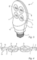
- FIG. 1 an exploded view of a flat lighting device, such as a flat lamp 1, is shown.
- the flat lamp 1 is shown in a standing manner defining a longitudinal axis A1.
- the flat lamp 1 comprises a carrier 2, like for instance a printed circuit board (PCB), a plurality of light sources 3, such as LEDs, OLEDs and PLEDs or the like, placed on the carrier 2, a plurality of lenses 4, a first cover member 5a and a second cover member 5b arranged to cover each side of the carrier 2, and a cap 6, adapted to be fitted in an electrical socket.
- PCB printed circuit board
- the carrier 2 may be a printed circuit board (PCB).
- PCB printed circuit board
- Different types of PCBs are commonly used like a PCB with an insulating core covered on both sides with a copper layer, or the carrier may be of the FR4 type, that is, an aluminium spreader provided with a PCB and thin copper layer on both sides of the aluminium.
- the carrier 2 defines a plane extending along the longitudinal axis A1, and is arranged in the cap 6.
- the electrical connection from the electrical socket may be directly coupled from the cap 6 to the carrier 2, or it may be wire connections between the cap 6 and the carrier 2. Further, the electrical connection may comprise additional electronic components, for instance for driving the light sources 3.
- the light sources 3 are arranged in separated subgroups, wherein each subgroup comprises two light sources 3. A subgroup may alternatively comprise one light source.
- the flat lamp 1 is symmetrically arranged, having four subgroups of light sources 3 placed on each side of the carrier 2 in the same pattern.
- the cover member 5a, 5b is adapted to support the lenses 4. Each lens 4 is arranged in front of a subgroup of light sources 3.
- the cover members 5a, 5b are adapted to be in thermal connection with the carrier 2 and transfer heat away from the heat source, i.e. the light source 3, via the carrier 2 and further to the ambient air.
- the cover members 5a, 5b are of a thermally conductive material such as plastic, glass, thermal plastic or ceramic or the like, preferably a material with low thermal resistivity.
- the second cover member 5b comprises a protrusion 9 with a corresponding opening or recess 8 on the carrier 2.
- the recess 8 and the protrusion 9 are arranged to align the carrier 2 and the cover members 5a, 5b correctly at assembly before joining the parts.
- the cover members 5a, 5b are arranged to cover a large part of the area of the carrier 2.
- the carrier 2 has a front side and a back side.
- the carrier 2 further comprises a layer of a thermally conductive material 7. This material may be spread evenly across the area of the carrier 2 on each side in order to spread any heat that may arise from the light sources 3.
- the material that may be used for the thermal conductive layer 7 may be any material with required thermal conductive properties, such as copper.
- An inner surface 11 of the respective cover members 5a, 5b is arranged to be in thermal contact with the front side and the back side, and preferably the thermally conductive layer, of the carrier 2 for good heat transfer.
- the heat transfer between the carrier and the cover member may be improved by providing a thermal interface material, TIM, in between.
- the TIM may be provided on either or both of the front side and back side of the carrier.
- the TIM may be arranged on the front and/or back side of the carrier to be pressed between the cover member and the printed circuit board.
- the TIM may fill irregularities in the surfaces of the carrier and the cover member, i.e. filling air gaps at the interface between the two.
- the TIM may be arranged to decrease the amount of trapped air in and prevent the presence of micro bubbles between the carrier 2 and the inside 11 of the cover member.
- the TIM has a higher thermal conductivity than air, and thereby increases the heat transfer between the carrier and the cover member.
- a flat lamp 1 according to the invention may be arranged to suit any size and shape of a retrofit lamp.
- the carrier 2 and the cover member 5 may be shaped and sized to suit any requirements.
- the flat lamp 1 may apply the shape of any standard or decorative lamp. It may also be possible that the carrier 2 has another shape than being flat.
- Each lens 4 is adapted to distribute the light from the light sources 3 in a predetermined manner according to a certain light scheme.
- the lens 4 may therefore be of a substantially transparent material, although possibly translucent.
- the lens 4 may also be arranged to transfer heat arising from the light source 3.
- the lenses 4 may be made from another material, hence separate from the cover member 5a, 5b, or alternatively fully incorporated in the cover member 5a, 5b.
- Fig. 2 an exploded view of the flat lamp 1 is shown, wherein the lenses 4 are integrated with the cover member 5a, 5b.
- the cover member 5 may thus constitute the same material as the lens 4, and thereby distribute some of the light emitted from the light source.
- the cover member 5a, 5b comprises two parts, a first part 5a and a second part 5b, to be arranged on each side of the carrier 2 and fastened together at a joint 10 along their rims.
- the cover member 5a, 5b may be arranged with the joint elsewhere, or if possible, cast in one single piece. It is further possible to assemble the two parts 5a, 5b of the cover member by a click arrangement.
- the joining may alternatively involve gluing or welding of the two parts 5a, 5b together, possibly along the outer rim of the cover member.
- the cover member may be joined by screwing, or any other joining operation that may be suitable and technically available.
- the cap 6 in Fig. 1 is provided with a thread to suit an electrical socket.
- the type of fitting of the cap 6 may however be different depending on the requirements.
- the fitting maybe arranged as a bayonet fitting, a pin fitting (such as of GU10 type) or any other fitting that may be suitable for a flat lamp 1. It may also be of any size suitable for that particular lamp 1.
- Fig. 3 shows a schematic view of a fully assembled flat lamp 1 as the one in Fig. 1 .
- Fig. 3 shows only one side of the carrier 2, having four separate lenses 4, one for each light source 3, that are fitted close to the cover member 5. It is possible that there is provided light sources 3 only on one side of the carrier 2.
- the cover member 5 may then be appropriately shaped to suit the arrangement. For example the cover member 5 may only be provided with lenses 4 on the side that contains any light sources 3.
- a flat lamp 1 according to the invention comprises light sources 3 on any or both sides of the carrier 2, as well as anywhere on the carrier 2. For instance, if it is required with a more directed light in one direction, a flat lamp may be adapted to spread light from one side of the carrier 2.
- direction of light may be altered by having different lenses 4.
- a symmetrically cut lens 4 may spread light virtually uniformly around the light source 3, while a non-symmetrically cut lens 4 may direct the light in a specific required direction. It is also a possibility that several light sources 3 share the lens 4. For example, a larger lens may be arranged to cover more than one light source 4. In the case of only having light sources 3 provided on a front side of the carrier 2, a back side of the carrier 2 may assist to transfer heat from the light sources 3, allowing the heat to transfer through the carrier 2 to a thermally conductive layer on the back side.
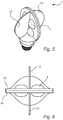
- Fig. 4 depicts a cross sectional view of a flat lamp 1, taken along a line perpendicularly to the longitudinal axis A1, across the lenses 4 in Fig. 3 .
- the cover member 5a, 5b is arranged closely to the carrier 2, so as to allow thermal contact, for the heat arising from each light source 3 to be transferred via the cover member to the ambient.
- the lens 4 in Fig. 4 is separate from the cover member, being arranged to be tightly held by the cover member against the carrier 2.
- the lens 4 in Fig. 4 has a flat surface arranged against the carrier 2 and a domed concave shape arranged above the light source 3. Externally, the lens 4 has a convex shape in order to spread the light evenly to its surroundings.
- the lens 4 has an inner cavity 14 adjacent the light source 3. The cut of the inner cavity 14 and the external surface of the lens 4 may differ in order to produce a required luminous intensity distribution to its surroundings or, whenever appropriate, add a more focused light in a certain direction.
- the cover member 5 may be provided with a second section 12 which is arranged with an angle with respect to the first section.
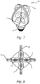
- Figs. 5 and 6 show a type of flat lamp 1 with a second section 12 of the cover member 5, in the shape of wings arranged perpendicular to the carrier 2.
- the second section 12 is preferably made from a thermally conductive material, possibly the same material as the cover member or such as a thermally enhanced plastic to improve thermal performance.
- the second section 12 may be arranged to improve design, strength, thermal and/or optical properties. For instance, the second section 12 may be reflective or refractive for better luminous intensity distribution.
- the second section 12 may be shaped and arranged anywhere suitable.
- the second section 12 may be shaped as ribs, fins or pins, arranged to improve thermal and/or optical performance.
- the wings, ribs, fins or pins forming the second section 12 can be placed at any angle relative to the cover members 5a, 5b. It is also possible to provide a number of light sources 3 on the second section 12, as shown on the crossed lamp 30 in Figs 7 and 8 , e.g. for higher lumen packages.
- the cover member may further be provided with openings to improve the thermal and optical properties of the arrangement.
- a crossed lamp 30 comprising multiple carriers 2, 15.
- the carriers 2, 15 are covered by a cover member 16, adapted to suit the crossed design.
- the light sources 3 may be placed anywhere appropriate as required.
- the lenses 4 are adapted accordingly regarding shape, size and cut, in order to provide the required luminous intensity distribution. Possibly, the lenses 4 are cut in a non-symmetrical way to reflect the light away from the centre of the crossed lamp 30.
- the second carrier 15 is angled differently relative to the first carrier 2. For instance, the angle between the first carrier 2 and the second carrier 15 may be larger or smaller than the shown 90 degrees. Further, it is possible that the two carriers 2, 15 do not cross each other, but are arranged in contact with each other under an angle.
- Fig. 9 shows a lamp as described according to Fig. 1 to which a ring 13 has been added for extra support longitudinally and transversally relative to the longitudinal axis A1, around the flat lamp 1.
- the ring 13 may provide support to a luminaire.
- the ring 13 may also be of a thermally conductive material, such as aluminum or the like, or of the same material as the cover members 5a, 5b, to provide improved thermal performance.
- the ring 13 can be located anywhere around the flat lamp 1.
- FIG. 10 there is shown an embodiment of a lamp having a double walled arrangement 40.
- This arrangement is designed having two carriers 18, 19 arranged in parallel relative to each other.
- the carriers 18, 19 are provided with a plurality of light sources 3 and lenses.
- the carriers 18, 19 are covered with a cover member 17, covering each of the carriers 18, 19.
- the parallel design may be required for instance if additional cooling of the carrier is required, and hence allowing the additional surface area of cover member 17 to transfer the additional heat arising from the light sources 3.
- the cover member 17 is, due to its complex design, arranged to be suitably assembled. For instance, the cover member 17 may be designed in a plurality of parts to be joined.
- Fig. 11 shows a flat lamp in the arrangement as a flat spot light 50.
- the flat spot light 50 comprises a carrier 21 arranged transversally relative to the longitudinal axis A1.
- the flat spot light 50 comprises a connection between the cap 6 and the carrier 21. This connection may be by an additional carrier arranged from the cap to the carrier 21, or alternatively another type of connection such as wire.
- the carrier 21 is provided with a plurality of light sources 3 and a cover member 20a, 20b.
- the first cover member 20a in Fig. 11 comprises a plurality of lenses 4, integrated in the cover member 20a.
- the cover members 20a, 20b may be made from the same type of material.
- the cover members 20a, 20b are made of different material, including the part of the second cover member 20b extending to the cap 6. It is also possible that the lenses 4 are separate from the first cover member 20a. Light sources and related optical structures may be arranged on one side or on both sides of the carrier 21. The carrier 21 may also be oriented differently relative to the longitudinal axis A1.
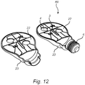
- Fig. 12 shows a flat lamp 60 comprising a first cover member 23 with lenses 4, and wherein the carrier is formed as an integrated part of an inner surface 22 of the first cover member 23.
- the electrical connections are printed on the inner surface 22 of the first cover member 23.
- Light sources 3 are arranged on the inner surfaces 22 of both parts of the first cover member 23.
- the second cover member is substantially identical to the first cover member 23.
- a lens 4 is arranged on one of the cover members with a corresponding light source 3 on the other cover member.
- the lenses 4 and light sources 3 are arranged in an alternated manner.
- a heat spreading layer may be arranged on the inner surface 22 to spread the heat generated by the light sources 3 over the inner surface 22.
- the optical structure for outcoupling the light from the lighting device comprises one or more lenses 4.
- lightguides or scattering optics can be used as optical structure.
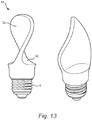
- Fig. 13 shows a flat lamp 65 in which the carrier (not shown) is shaped as a double-helical surface. This surface extends in the direction of the longitudinal axis A1.
- This carrier can be sandwiched in between the two cover members 5a, 5b.
- This embodiment is further similar to the construction of the embodiment as shown in e.g. Fig.1 . It may comprise one or more light sources, such as LEDs, mounted on the carrier and a light-transmitting part of the cover members to enable light exiting from the light sources 3.
- the double-helical or twisted embodiment has the advantage that the desired luminous intensity distribution will at least partly be determined by the amount of twist between the lower side, near the connection member, and the upper side of the carrier.
- the effect of the improved luminous intensity distribution is caused by the fact that in a double-helical structure the orientation of the normal of the double-helical surface relative to the longitudinal axis A1 of the lighting device is not constant. The normal of a first portion of the surface is different from the normal of a second portion.
- a solid state light source mounted on a carrier emits light with the central axis of its emission profile pointing in the direction of the normal of the surface at the position the solid state light is mounted.
- the twisted or curved shaped of the carrier enables an improved light distribution around the lighting device.
- the twist angle between a first end of the double-helical surface pointing in the direction of the connection member, and a second end pointing away from said connection member should differ by an angle that is in the range between 15° and 360°. If so desired, the amount of twist may also be larger than 360°.
- this twist angle is chosen between 60° and 180°, better results with a twist angle of about 90°.
- the twist angle is about 120°.
- Such a design enables it to obtain a unform luminous intensity distribution without applying any optical structures in front of the LEDs, by redirecting the light emitted by the light sources arranged on the carrier. It is evident that a combination of a twisted carrier with optical structures like lenses, light guides or scattering optics is possible as well..
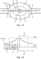
- the thermal properties of a lighting device according to the present invention are determined by a short thermal path between the solid state light source 3 and the outside of the cover members 5a, 5b, where the heat is dissipated to the ambient. This is realized, as illustrated in Fig. 14 , by a solid state light source 3 disposed on a carrier 2 to which the heat generated by the solid state light 3 source is transferred, indicated by arrows 70.
- the thermal interface from the carrier 2 to the cover members 5a, 5b and the optical structure 4 ensures a short thermal path to the outside of the lighting device 1.
- the carrier 2 comprises a thermally conductive material which has a first coefficient of thermal conductivity and the cover members 5a, 5b have a second coefficient of thermal conductivity, the first coefficient of thermal conductivity being larger than the second coefficient of thermal conductivity.
- the first coefficient of thermal conductivity should be sufficiently large to spread the heat from the solid state light source over the full carrier 2 with a small temperature drop (arrow 71), the second coefficient of thermal conductivity being sufficient to get a small temperature drop over the thickness of the cover (arrows 72,73).
- the required first coefficient of thermal conductivity is connected to the thickness of the thermally conductive material on the carrier 2 and the effective heat transfer coefficient from the cover members 5a, 5b to the ambient.
- the ratio of heat conduction over heat transfer to ambient should be sufficient, as is explained by the fin efficiency theory.
- the second coefficient of thermal conductivity should have a minimum value to keep the temperature drop over the cover thickness limited, e.g. 0.2 W/mK which is typical for standard engineering plastics.
- the first coefficient of thermal conductivity is in the range from 100-300 W/mK, preferably between 160 and 240 W/mK
- the second coefficient of thermal conductivity is in the range from 0.2-10 W/mK, preferably between 0.5 and 5 W/mK.
- the thermal behavior of the lighting device is determined by a number of parameters in the design of the lighting device.
- retrofit lamps When designing lighting devices with LEDs meant for replacing the well-known incandescent lamps, also referred to as retrofit lamps, it is required to have a design in which the thermal conductivities in combination with the surface that radiates the heat to the ambient ensures a maximum temperature of the lighting device in order to safeguard its life time performance.
- the design considerations are given for retrofit lamps with different light output levels. Table 1.
- the required thermal resistance R th is calculated for retrofit lamps with different light output.
- the range from 450-1600 lumen roughly coincides with incandescent bulb with a power consumption between 40 and 100 W.
- the system efficacy (that is the amount of light generated per watt power used by the LED system) is about 80 lm/W at a lumen equivalent of 300 lm/W (that is the amount of light per watt light power).
- the heat load is calculated; this heat load is the amount of heat that is generated but that is not transferred to light. So, this is the amount of heat that should be radiated from the lighting device, for instance by cooling.
- the last column shows that these required surfaces can be realized in a retrofit design for the desired lumen values in terms of the sizes used for the well-known incandescent bulbs.
- the 1600 lumen design can also be made with an A21 type lamp, but in this case a two-fin construction, as for instance given in Fig. 10 is required in order to have sufficient area for cooling.
- the fin efficiency as given in Table 2 is determined by the spreading of the heat over the carrier 2.
- Fig. 15 which model schematically shows a solid state light source 3 in a carrier 2 and the thermal behavior of this light source.
- the light source heats up to T max at an ambient temperature T amb .
- the temperature in the fin that is understood to be the overall environment of the light source
- the effective size L eff 81 of the fin is determined by the demand that the area defined by L eff and a constant temperature T max is equal to the area under the curve of the fin temperature until the apparent size L app 82 of the fin.
- L app is determined by the geometrical design of the lighting device 1. In this example an L app of 2 cm has been chosen, meaning that it is assumed that the heat dissipated in a light source is distributed through the carrier over a distance of 2 cm. Further, in this formulae:
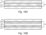
- the fin efficiency was determined for two different types of carrier, which are shown in Fig. 16A and B .
- the first type - Fig. 16A - is a standard PCB design of a carrier 2 with a PCB core 90 covered on both sides with a copper layer 91 of thickness of 35 ⁇ m and of 70 ⁇ m, with a first coefficient of thermal conductivity of 400 W/mK.
- the second type - Fig. 16B - is a carrier 2 with an aluminium spreader 92 with thickness of 0.2 mm and 0.5 mm provided with a PCB core 93 and thin copper layer 94 (FR4 type) on both sides of the aluminium, and a first coefficient of thermal conductivity of 200 W/mK .
- FR4 type thin copper layer 94
- the lighting device 1 may comprise a controller adapted to control each of the at least one solid state light sources individually.
- the controller may be integrated in the printed circuit board for the at least one solid state light source and may further contribute to the compact lighting device with few parts.
- the controller may further be adapted to control the light sources separately.
- the controller may control the light sources to different color, different luminous intensity distribution etc.
- the different luminous intensity distribution may comprise different beam shapes of the light output from the light sources.
- the shape of the carrier and cover member may be different, and the locations of the light sources may be optional. For instance, not only flat bulb shapes are possible, but any shapes desired such as square shapes, angled shapes or heart shapes.
Description
- The present invention relates to flat lighting device comprising solid state light sources, and more specifically to flat lamp.
- Conventional LED lamps comprise a printed circuit board with LEDs arranged onto it. The printed circuit board is arranged in a horizontal manner when arranging the LED lamp in a standing position, or, if defining a longitudinal axis of the LED lamp, arranged with an angle to the longitudinal axis. In front of the printed circuit board in a light exit direction, a plastic or glass bulb is arranged in order to manipulate the emitted light from the LEDs, and to protect components inside the lamp. Below the printed circuit board, a number of components are arranged with the main purpose of spreading and transferring the heat generated by the LEDs. These may be a heat spreader, heat fins, a metal housing and a cap. Such LED lamp hence comprises a large number of components in order to perform all tasks of the lamp such as generating and distributing light, transferring heat, protect the electric connections and provide a fire enclosure.
- An alternative LED lamp is disclosed in
WO2011/107925A1 , wherein a printed circuit board with a LED is arranged on a reflector. Such solution decreases the amount of components in the lamp. However, such lamp has its limitations in optical and thermal performance. Further, such arrangement may be sensitive to physical actuation and may not provide sufficient thermal properties for high lumen lamps. - Consequently, there is a need for a lamp that in a protective manner further increases the effectiveness in terms of optical and thermal properties.
US 2007/0121326 discloses a lighting device with a cover member enclosing a carrier, wherein the cover member serves also as a heat dissipation element.DE 10 2011 006 749 discloses a lighting device with a carrier covered by an electrically isolating element to prevent electrical shocks to the user.US 2012/0069570 discloses a lighting device with a central carrier surrounded by a cover manufactured in two pieces.US 2010/0181885 discloses a lighting device with a carrier covered on its front and back surfaces by two heat sinks. - It is an object of the present invention to provide a lighting device that provides an effective heat management.
- According to a first aspect of the invention, this isachieved by a lighting device comprising all the technical features of
claim 1. It is recognized by the present invention that the desired thermal properties of a lighting device can be achieved by having a short thermal path between the light source and the outside of the cover, where the heat is dissipated to the ambient. This is realized by a solid state light source disposed on a carrier to which the heat transmitted by the solid state light source is transferred. The thermal interface from the carrier to the cover member ensures a short thermal path to the outside of the lighting device. - This improved thermal performance is preferably realized when the carrier comprises a thermally conductive material having a first coefficient of thermal conductivity and the cover having a second coefficient of thermal conductivivity, the first coefficient of thermal conductivity being larger than the second coefficient of thermal conductivity.
- In this way the heat is largely and quickly transferred to the carrier in the vicinity of the solid state light source, after which it is transferred via the thermal interface to the cover member, and from the outside of the cover member to the ambient. Preferably, the heat is radiated to the ambient in substantially the same direction of the light emission, meaning that the heat leaves the lighting device on the same side as the light..
- In a preferred embodiment, the first coefficient of thermal conductivity is in the range from 100-300 W/mK, preferably between 160 and 240 W/mK, and the second coefficient of thermal conductivity is in the range from 0.2-10 W/mK, preferably between 0.5 and 5 W/mK.
- In a further embodiment, the thermal conductive material is disposed as a thermal conductive layer on the carrier. This is, for instance, the case when the carrier is a printed circuit board, being the most familiar type of carrier. This conductive layer may be a metal layer like e.g. copper, which also shows an excellent electrical conductivity. Therefore, it can be used for making the electrical connections of the solid state light sources to the driver part of a lighting device.
- The thermal performance can further be improved by a thermal interface material, TIM that is arranged to fill a space between the cover member and the carrier. The TIM may be sandwiched between the cover member and the printed circuit board. The TIM may be provided on either or both of the front side and back side of the printed circuit board. The TIM may fill irregularities in the surfaces of the printed circuit board and the cover member, i.e. filling air gaps at the interface between the two. The TIM has a higher thermal conductivity than air, and thereby increases the heat transfer between the printed circuit board and the cover member.
- In this aspect of this invention, it is realized that this lighting device may further comprise a connection member having a fixed position relative to the carrier for mechanically and electrically connecting the lighting device to a socket. The carrier is having a relatively large front side compared with its edge side and the solid state light source is arranged on the front side of the carrier. The cover member has an outer surface being a portion of the outside of the lighting device and has an inner surface, opposite to the outer surface, that is in thermal contact with the front side of the carrier, such that the thermal interface is formed.
- In this embodiment the present invention is applied to make, for instance a lighting device that is suitable for replacing a conventional incandescant type of lamp, also referred to as a retrofit lamp.
- In a further embodiment, a second solid state light source arranged on a back side of the carrier being opposite to the front side, a second cover member disposed on the carrier, whereby the second light source is arranged between the carrier and a light-transmitting part of the second cover member, such that a thermal interface exists between the carrier and the second cover member, the second cover member having a second outer surface being a second portion of the outside of the lighting device and having a second inner surface being opposite to the second outer surface and being in thermal contact with the back side of the carrier, such that the second thermal interface is formed.
- In this embodiment the front side and the back side of the lighting device may be constructed in a similar way. When this is used a retrofit lamp can be obtained that emits light in both direction respective to the front side and back side.
- The thermal performance of these embodiments is ensured when at least 50%, preferably 90% of the front side of the carrier is in thermal contact with the inner surface of the cover member. The heat is dissipated by the solid state light sources and spread to the surroundings of the solid state light sources via the carrier; the larger the part of the carrier that is in thermal contact with the cover member, the better the heat transfer is from the carrier to the cover member.
- According to a first aspect of the invention, this and other objects are achieved by a lighting device comprising a planar carrier including a thermally conductive layer, at least one solid state light source arranged on a front side of the carrier, and an insulating cover member in thermal contact with said front side and a back side opposite said front side, and said cover member being adapted to transfer heat from said carrier out of the lighting device. The cover member comprises an optical structure arranged on the carrier in front of the at least one light source and adapted to direct the light emitted by the at least one solid state light source.
- Such lighting device may thereby provide an effective heat transfer from the printed circuit board and out of the arrangement with few parts and in a compact manner. Due to the thermal contact of the cover member with both sides of the printed circuit board, a majority of the heat generated by the light sources may be transferred by the cover member. The cover member may be in direct contact with the printed circuit board. The cover member may comprise an inner surface facing the printed circuit board. The inner surface may be in direct contact with the front and back side of the printed circuit board. The lighting device may further provide a cost efficient manufacturing process due the few parts. The an optical structure may be designed to direct the light from the light source through the cover member in a desired way. The light source and the printed circuit board may together provide the functions of converting power, generating light and spreading the heat generated. The cover member and lens may provide the functions of manipulating/directing the light from the light source, transferring the heat from the printed circuit board and providing electrical insulation and fire enclosure of the arrangement. The cover member may further have a protective purpose, protecting the printed circuit board and light source from external damage. The lighting device may be arranged in a cap for use in an electrical socket, or integrated in a luminaire. The printed circuit board may comprise two flat sides, the front side and the back side. The printed circuit board may further be planar. Light sources may be arranged on either one or both sides of the printed circuit board. The cover member may be arranged such that it is in thermal contact with both sides of the printed circuit board. The cover member may be arranged to be in thermal contact with a substantial part of the printed circuit board, such as at least half of the front side and back side of the printed circuit board. The cover member may be formed of a glass material, a plastic material, a ceramic material or the like. A normal plastic material for a cover member may provide sufficient thermal properties to provide a heat transfer function from the printed circuit board. To further improve the thermal properties of the cover member, the cover member may be made of a thermal plastic material. The printed circuit board may comprise a heat spreading layer for spreading the heat generated by the light sources over a large area of the printed circuit board. The heat spreading layer may for instance be a copper layer or an aluminum layer. The heat spreading layer may further be adapted to spread heat from the front side to the back side of the printed circuit board, and vice verse. In one embodiment, the printed circuit board may comprise more than one heat spreading layer. Further, in one embodiment, the printed circuit board may comprise an aluminum sheet metal provided with electrical connections of FR-4 or CEM-1 material. The aluminum sheet metal may thereby form the heat spreading layer and electrical interconnections. The cover member is arranged to enclose the printed circuit board and the at least one solid state light source. Wherein the cover member encloses the printed circuit board, and is in contact with both the front side and the back side of the printed circuit board, the cover member may provide the required stiffness to the arrangement in order to hold the printed circuit board. The printed circuit board may then be made very thin, for instance as thin as 0.2 mm. Since the cover member encloses both front and back side of the printed circuit board, the printed circuit board will anyway be held in place. The printed circuit board thereby does not need to provide stability to the arrangement, but may be focused on heat spreading, holding the light source and providing electrical tracks to the light source. By enclosing the printed circuit board, the cover member may be in thermal contact with a large part of the printed circuit board, such as at least ninety percent of an external surface of the printed circuit board. The cover member may further be in thermal contact with edge surfaces of the printed circuit board. The edge surfaces may together with the front side and back side form a total external surface of the printed circuit board. The heat transfer from the printed circuit board may thereby be improved. The cover member may have an inner side and an outer side, wherein the inner side is in contact with the printed circuit board and adapted to transfer heat from the inner side to the outer side.
- The cover member may in one embodiment be formed of a transparent material and the lens may be formed as an integrated part of the cover member. The cover member and the lens may be formed of the same material in one piece. The material of the cover member including the lens may thereby provide both the thermal properties for heat transfer and the optical properties of the lens, directing the light from the light source. The material may be transparent or translucent due to the optical properties. The cover member and lens may be molded in one common piece. Alternatively, the cover member may be formed of a thermally conductive material, and as a separate part from the an optical structure which is formed of a transparent or translucent material. The lens may be formed of a material different from the material of the cover member. The material of the cover member may be designed for providing good heat transfer properties, such as a material with low thermal resistivity. The cover member may be non-transparent. The different material of the lens may be designed for good optical performance in directing the light from the light source. The lens may however have some thermal conductivity, i.e. contribute to the heat transfer from the printed circuit board. An inner side surface of the lens, which may be in contact with the printed circuit board, may be designed to maximize the heat transfer from the printed circuit board to the lens. Such inner side surface may be flat. The cover member comprises a first and a second cover part adapted to be attached to each other and to be in contact with the front side and the back side of the printed circuit board respectively. The cover member may be in two parts, thereby facilitating the manufacturing and the assembly of the lighting device. The two parts may comprise fastening means arranged to mate with each other in order to be fixed the two parts to each other. Such fastening means may be a snap coupling, glue, screws, ultrasonic welding or the like. The printed circuit board may be sandwiched between the two cover parts when assembled. The first cover part may thereby be in thermal contact with the front side of the printed circuit board, and the second cover part may be in thermal contact with the back side of the printed circuit board. Further the first cover part may comprise a protrusion adapted to extend through an opening in the printed circuit board to align the printed circuit board inside the cover member. To align the printed circuit board inside the cover member, the cover member may comprise a protrusion extending through an opening in the printed circuit board. The position of the printed circuit board relative to the cover member may thereby be fixed. The protrusion on the first cover part may be adapted to mate with corresponding means on the second cover part, thereby fixing the two parts to each other and sandwiching the printed circuit board in between.
- In a further embodiment, the at least one solid state light source may comprise a plurality of solid state light sources arranged with a distance to each other, or arranged in subgroups with a distance between each subgroup, and wherein the an optical structure may comprise a number of lenses equal to the number of separated solid state light sources or the number of separated subgroups of solid state light sources. To provide a lighting device which provides a light output of a certain amount, a plurality of light sources may be arranged on the printed circuit board. The plurality of lenses may each be designed to direct light from one light source or a subgroup of light sources arranged together. By spreading the light sources or subgroups of light sources on the printed circuit board, the heat generated by the light sources may further be spread along the extension area of the printed circuit board. This may improve the heat spreading and heat transfer function of the arrangement due to a more efficient heat spreading in the printed circuit board, which provides a more efficient heat transfer by the cover member. By providing a number of lenses equal to the number of light sources or subgroups of light sources, the total light output from the lighting device may be highly controllable. The lens for a specific light source or subgroup of light sources may be specially designed for that light source or subgroup, and may be different from another lens for another light source or subgroup. For instance, the light output may be directed in certain directions by each lens such that the total light output is optimized for a specific purpose. Further, each light source or subgroup may be controlled by a driver or controller to provide a light output unique for that specific light source or subgroup.
- In one embodiment, the lighting device may have a longitudinal axis and the printed circuit board may extend in a first plane in parallel with the longitudinal axis. The lighting device may further comprise a cap, and wherein the printed circuit board is arranged on said cap. The cap may be adapted to fit in an electrical socket. The arrangement of the printed circuit board in the cap, extending in a plane along the longitudinal axis may provide a lighting device with few parts. The longitudinal axis may extend through the center of the cap. The at least one light source arranged on the printed circuit board may thereby emit light in a main direction which is perpendicular to the longitudinal axis. The lens may however direct light in a plurality of directions, including a direction substantially in parallel with the longitudinal axis. The cover member, which encloses the printed circuit board, thereby extends in the same plane as the printed circuit board, and also be arranged in said cap. The cover member, the an optical structure, and the cap may provide an entire outer surface of the lighting device, together enclosing the printed circuit board and the at least one light source.
- Alternatively, the printed circuit board may extend in a plane perpendicular to said longitudinal axis. The printed circuit board may thereby be arranged with light sources providing a spotlight arrangement. The cover member may be arranged to be in contact with both the front and back side of the printed circuit board in order to provide the same thermal properties as for a lighting device with a printed circuit board in parallel with the longitudinal axis.
- In another embodiment, a first section of the cover member encloses the printed circuit board extending in said first plane, and wherein a second section of the cover member extends in a second plane with an angle to said first plane. A further extension of the cover member may improve the heat transfer capability of the cover member due to a larger surface exposed to the surroundings of the lighting device. The second section of the cover member may extend in parallel with the longitudinal axis. The two sections of the cover member may thereby form a cross shaped cross section when seen in direction of the longitudinal axis. Alternatively may the second plane be transverse to the longitudinal axis as well as the first plane. If an outer surface of the cover member is a reflective surface, or is provided with a reflective coating, the second section of the cover member may improve the optical performance of the lighting device. Yet alternatively, for a spotlight arrangement, the second plane may be in parallel with the longitudinal axis, and with an angle to the first plane. The cover member may comprise further additional sections, such as a third and a fourth section. The sections may form various formations. For instance three sections of the cover member may form a triangle shape. Further, the printed circuit board may be a first printed circuit board, and wherein the lighting device further comprises a second printed circuit board enclosed by the second section of the cover member. The second printed circuit board may be arranged to extend in said second plane transversal to the first plane in which the first printed circuit board extends. The second printed circuit board may be provided with at least one solid state light source. The second section of the cover member may be provided with an optical structure corresponding to the light source on the second printed circuit board. By providing the second printed circuit board and the light source thereon, light may be emitted from the lighting device in additional directions. The optical performance of the lighting device may thereby be improved.
- In one embodiment, the optical structure may be designed to provide non-symmetric optical properties. The optical structure may be designed to direct the light from the at least on solid state light source in a non-symmetrical manner, providing a non-rotational symmetry of the luminous intensity distribution. That is, a circular or dome shaped lens may provide a non-uniform light output along its light output directions. When the arrangement comprises a plurality of light sources and a plurality of lenses, the lenses may be non-symmetrically designed such that the overall light output from the arrangement is uniform or in an otherwise desired way. The non-symmetric lens may be designed to direct a minimum amount of light towards a neighboring lens. The lens may comprise an inner cavity, which inner cavity surrounds the light source(s) which the lens is arranged in front of. The inner cavity may be shaped in order to provide the non-symmetric luminous intensity distribution of the lens. Due to the shape of the inner cavity, the refraction of the light from the light source(s) reaching the lens may provide a desired luminous intensity distribution. Alternatively, the non-symmetry of the lens may be provided by the design of an outer surface of the lens.
- In an alternative embodiment, said printed circuit board may be a first printed circuit board with a first front and back side having at least one solid state light source arranged on the first front side, wherein the lighting device further may comprise a second printed circuit board with a second front and back side and having at least one solid state light source arranged on said second front side, and wherein said second printed circuit board is arranged in parallel with said first printed circuit board. A lighting device comprising two flat light source holding plates in the same cap may provide an arrangement with an improved thermal resistance. I.e. the thermal resistance of the cover member in thermal contact with both printed circuit boards may be lowered. The cover member may be in thermal contact with the front sides and back sides of both printed circuit boards. The cover member may enclose both the first and the second printed circuit boards. Each front side of the printed circuit boards may be provided with one or more light sources. The two front sides may be directed in opposite directions. Heat from the light sources on the front sides may be spread also to the respective back side, thereby increasing the thermal performance of the arrangement.
- In an alternative embodiment, the printed circuit board may be formed as an integrated part of the cover member. The printed circuit board may be a part of an inner surface of the cover member. The electrical connections of the printed circuit board may be printed directly on said inner surface of the cover member, and the light sources may be arranged on said inner surface.
- In one embodiment, the printed circuit board and the cover member may have a curved shape. The printed circuit board may extend in a bent or curved plane which has a radius. The cover member may have a corresponding shape and be in thermal contact with the front and back side of the curved printed circuit board. A flexible board material may be used for forming the printed circuit board. Such formed lighting device may in some embodiments provide improved optical performance of the arrangement.
- Further, the printed circuit board may be a first printed circuit board and the lighting device may further comprise a second and a third printed circuit board, wherein the three printed circuit boards may be arranged with angles relative each other, and wherein the cover member may be in thermal contact with a front side and a back side of all printed circuit boards. An arrangement with the thermal properties and compact arrangement of the present invention may thereby be used in an embodiment with improved optical performance. The three printed circuit boards may be arranged, each with a longitudinal edge in contact with corresponding edges of the other printed circuit boards. Such longitudinal edge may coincide with a longitudinal axis of the lighting device. The printed circuit board may form a star like shape of the lighting device. The lighting device may also comprise further printed circuit boards forming other shapes and providing other optical performance, which may be desired in certain applications.
- In another embodiment, the printed circuit board may have a buckled surface forming two printed circuit board sections extending with an angle to each other. In this embodiment, buckled means that the two carrier sections are coupled to each other in such a way that the two carrier sections may be directed slightly differently, forming an angular bent shape of the carrier. Both carrier sections may be provided with light sources which thereby may emit light in different directions. The two carrier sections may be arranged in parallel with a longitudinal axis of the lighting device, but with an angle relative to each other. Alternatively, both sections may be arranged in parallel with an axis perpendicular to the longitudinal axis.
- In another embodiment, the carrier is a double-helical shaped surface positioned in parallel to the longitudinal axis. This shape has the advantage that the solid state light sources that are connected to the carrier are now directed in other directions than only perpendicular to the longitudinal axis. Note that the double-helical shaped surface has the property that a normal to this surface is in general not perpendicular to the longitudinal axis of the lighting device. This will lead to a lighting device having a more uniform luminous intensity distribution. Preferably, the double-helical surface has a first end pointing in the direction of the connection member, and a second end pointing away from said connection member, wherein the respective orientations of double-helical surface perpendicular to the longitudinal axis at the first end and at the second end differ by an angle in the range from 15° - 360°. A uniform light distibution may be realized when the respective orientations differ by about 90°, even a difference in orientation of about 45° may give an acceptable performance.
- For the embodiments that comprise the second solid state light source, the lighting device may comprise electical connections for independently powering the solid state light source and the second solid state light source. This has the advantage that different light sources, for instance those on the front side and those on the back side, can be addressed independently. This may be for indendently switching them on and off, but it may also be for dimming or colour changing aspects.
- It is noted that the invention relates to all possible combinations of features recited in the claims.
- Various aspects of the invention, including its particular features and advantages, will be readily understood from the following detailed description and the accompanying drawings, in which:
-
Fig. 1 is an exploded view of a lighting device according to an embodiment of the invention, comprising optical structures in the form of separate lenses; -
Fig. 2 is an exploded view of a lighting device according to an embodiment of the invention, comprising optical structures in the form of lenses integrated in the cover members; -
Fig. 3 is a perspective view of a lighting device according to an embodiment of the invention; -
Fig. 4 is a cross-sectional view across the lens of thelighting device ofFig. 3 ; -
Fig. 5 is a perspective view of a lighting device according to an embodiment of the invention comprising ribs; -
Fig. 6 is a top view of the lighting deviceofFig. 5 ;Fig. 7 is a perspective view of a lighting device according to an embodiment of the invention comprising orthogonally arranged carriers; -
Fig. 8 is a cross sectional view, seen in the direction of the longitudinal axis across the lenses of the lighting device ofFig. 7 ; -
Fig. 9 is a perspective view of a lighting device according to an embodiment of the invention, comprising additional longitudinal and transverse rings; -
Fig. 10 is a perspective view of a lighting device according to an embodiment of the invention comprising multiple parallel-arranged carriers; -
Fig. 11 is a perspective view of a lighting device according to an embodiment of the invention in the arrangement of a flat spot type of lamp; -
Fig. 12 is a perspective view of a lighting device according to an embodiment of the invention, with the carrier formed as an integrated part with the cover member; -
Fig. 13 is a side view of a lighting device according to an embodiment of the invention, comprising a cover member with a double-helical surface; -
Fig. 14 is a portion of the lighting device according to the present invention, indicating the heat flow through the device; -
Fig. 15 is an explanatory figure for the thermal model of the lighting device; -
Fig. 16A and 16B give two different examples of a carrier for use in the lighting device. - The present invention will now be described more fully hereinafter with reference to the accompanying drawings, in which currently preferred embodiments of the invention are shown. This invention may, however, be embodied in many different forms and should not be construed as limited to the embodiments set forth herein; rather, these embodiments are provided for thoroughness and completeness, and fully convey the scope of the invention to the skilled person. Like reference characters refer to like elements throughout.
- In
Fig. 1 , an exploded view of a flat lighting device, such as aflat lamp 1, is shown. Theflat lamp 1 is shown in a standing manner defining a longitudinal axis A1. Theflat lamp 1 comprises acarrier 2, like for instance a printed circuit board (PCB), a plurality oflight sources 3, such as LEDs, OLEDs and PLEDs or the like, placed on thecarrier 2, a plurality oflenses 4, afirst cover member 5a and asecond cover member 5b arranged to cover each side of thecarrier 2, and acap 6, adapted to be fitted in an electrical socket. - The
carrier 2 may be a printed circuit board (PCB). Different types of PCBs are commonly used like a PCB with an insulating core covered on both sides with a copper layer, or the carrier may be of the FR4 type, that is, an aluminium spreader provided with a PCB and thin copper layer on both sides of the aluminium. - The
carrier 2 defines a plane extending along the longitudinal axis A1, and is arranged in thecap 6. The electrical connection from the electrical socket may be directly coupled from thecap 6 to thecarrier 2, or it may be wire connections between thecap 6 and thecarrier 2. Further, the electrical connection may comprise additional electronic components, for instance for driving thelight sources 3. In the illustrated embodiment, thelight sources 3 are arranged in separated subgroups, wherein each subgroup comprises twolight sources 3. A subgroup may alternatively comprise one light source. Theflat lamp 1 is symmetrically arranged, having four subgroups oflight sources 3 placed on each side of thecarrier 2 in the same pattern. Thecover member lenses 4. Eachlens 4 is arranged in front of a subgroup oflight sources 3. Thecover members carrier 2 and transfer heat away from the heat source, i.e. thelight source 3, via thecarrier 2 and further to the ambient air. Thecover members - The
second cover member 5b comprises a protrusion 9 with a corresponding opening or recess 8 on thecarrier 2. The recess 8 and the protrusion 9 are arranged to align thecarrier 2 and thecover members cover members carrier 2. Thecarrier 2 has a front side and a back side. Thecarrier 2 further comprises a layer of a thermallyconductive material 7. This material may be spread evenly across the area of thecarrier 2 on each side in order to spread any heat that may arise from thelight sources 3. The material that may be used for the thermalconductive layer 7 may be any material with required thermal conductive properties, such as copper. By adding alayer 7 of a thermally conductive material, the heat may be evenly distributed across thecarrier 2, therewith reducing the number of zones with excessive heat, and the heat is transported through thecover members - An
inner surface 11 of therespective cover members carrier 2 for good heat transfer. - The heat transfer between the carrier and the cover member may be improved by providing a thermal interface material, TIM, in between. The TIM may be provided on either or both of the front side and back side of the carrier. In order to increase the heat transfer between the
carrier 2 and thecover members carrier 2 and thecover members - The TIM may be arranged on the front and/or back side of the carrier to be pressed between the cover member and the printed circuit board. The TIM may fill irregularities in the surfaces of the carrier and the cover member, i.e. filling air gaps at the interface between the two. The TIM may be arranged to decrease the amount of trapped air in and prevent the presence of micro bubbles between the
carrier 2 and the inside 11 of the cover member. The TIM has a higher thermal conductivity than air, and thereby increases the heat transfer between the carrier and the cover member. - A
flat lamp 1 according to the invention may be arranged to suit any size and shape of a retrofit lamp. Thecarrier 2 and thecover member 5 may be shaped and sized to suit any requirements. For instance theflat lamp 1 may apply the shape of any standard or decorative lamp. It may also be possible that thecarrier 2 has another shape than being flat. - Each
lens 4 is adapted to distribute the light from thelight sources 3 in a predetermined manner according to a certain light scheme. Thelens 4 may therefore be of a substantially transparent material, although possibly translucent. Thelens 4 may also be arranged to transfer heat arising from thelight source 3. Depending on a number of choices, such as material, manufacture, luminous intensity distribution requirements, heat properties and such, thelenses 4 may be made from another material, hence separate from thecover member cover member - In
Fig. 2 , an exploded view of theflat lamp 1 is shown, wherein thelenses 4 are integrated with thecover member cover member 5 may thus constitute the same material as thelens 4, and thereby distribute some of the light emitted from the light source. In order to ensure complete coverage of thecarrier 2, thecover member first part 5a and asecond part 5b, to be arranged on each side of thecarrier 2 and fastened together at a joint 10 along their rims. Depending on manufacturing and assembly capabilities, thecover member parts parts - The
cap 6 inFig. 1 is provided with a thread to suit an electrical socket. The type of fitting of thecap 6 may however be different depending on the requirements. For instance the fitting maybe arranged as a bayonet fitting, a pin fitting (such as of GU10 type) or any other fitting that may be suitable for aflat lamp 1. It may also be of any size suitable for thatparticular lamp 1. -
Fig. 3 shows a schematic view of a fully assembledflat lamp 1 as the one inFig. 1 .Fig. 3 shows only one side of thecarrier 2, having fourseparate lenses 4, one for eachlight source 3, that are fitted close to thecover member 5. It is possible that there is providedlight sources 3 only on one side of thecarrier 2. Thecover member 5 may then be appropriately shaped to suit the arrangement. For example thecover member 5 may only be provided withlenses 4 on the side that contains anylight sources 3. It is possible that aflat lamp 1 according to the invention compriseslight sources 3 on any or both sides of thecarrier 2, as well as anywhere on thecarrier 2. For instance, if it is required with a more directed light in one direction, a flat lamp may be adapted to spread light from one side of thecarrier 2. Also, direction of light may be altered by havingdifferent lenses 4. A symmetrically cutlens 4 may spread light virtually uniformly around thelight source 3, while anon-symmetrically cut lens 4 may direct the light in a specific required direction. It is also a possibility that severallight sources 3 share thelens 4. For example, a larger lens may be arranged to cover more than onelight source 4. In the case of only havinglight sources 3 provided on a front side of thecarrier 2, a back side of thecarrier 2 may assist to transfer heat from thelight sources 3, allowing the heat to transfer through thecarrier 2 to a thermally conductive layer on the back side. -
Fig. 4 depicts a cross sectional view of aflat lamp 1, taken along a line perpendicularly to the longitudinal axis A1, across thelenses 4 inFig. 3 . Thecover member carrier 2, so as to allow thermal contact, for the heat arising from eachlight source 3 to be transferred via the cover member to the ambient. Thelens 4 inFig. 4 is separate from the cover member, being arranged to be tightly held by the cover member against thecarrier 2. Thelens 4 inFig. 4 has a flat surface arranged against thecarrier 2 and a domed concave shape arranged above thelight source 3. Externally, thelens 4 has a convex shape in order to spread the light evenly to its surroundings. Thelens 4 has aninner cavity 14 adjacent thelight source 3. The cut of theinner cavity 14 and the external surface of thelens 4 may differ in order to produce a required luminous intensity distribution to its surroundings or, whenever appropriate, add a more focused light in a certain direction. - The
flat lamp 1 according to the invention, thecover member 5 may be provided with asecond section 12 which is arranged with an angle with respect to the first section.Figs. 5 and 6 , show a type offlat lamp 1 with asecond section 12 of thecover member 5, in the shape of wings arranged perpendicular to thecarrier 2. Thesecond section 12 is preferably made from a thermally conductive material, possibly the same material as the cover member or such as a thermally enhanced plastic to improve thermal performance. Thesecond section 12 may be arranged to improve design, strength, thermal and/or optical properties. For instance, thesecond section 12 may be reflective or refractive for better luminous intensity distribution. Thesecond section 12 may be shaped and arranged anywhere suitable. For instance, thesecond section 12 may be shaped as ribs, fins or pins, arranged to improve thermal and/or optical performance. The wings, ribs, fins or pins forming thesecond section 12 can be placed at any angle relative to thecover members light sources 3 on thesecond section 12, as shown on the crossedlamp 30 inFigs 7 and 8 , e.g. for higher lumen packages. The cover member may further be provided with openings to improve the thermal and optical properties of the arrangement. - In
Fig. 7 and 8 a crossedlamp 30 is shown comprisingmultiple carriers carriers carriers cover member 16, adapted to suit the crossed design. Thelight sources 3 may be placed anywhere appropriate as required. Thelenses 4 are adapted accordingly regarding shape, size and cut, in order to provide the required luminous intensity distribution. Possibly, thelenses 4 are cut in a non-symmetrical way to reflect the light away from the centre of the crossedlamp 30. It is possible that thesecond carrier 15 is angled differently relative to thefirst carrier 2. For instance, the angle between thefirst carrier 2 and thesecond carrier 15 may be larger or smaller than the shown 90 degrees. Further, it is possible that the twocarriers -
Fig. 9 shows a lamp as described according toFig. 1 to which aring 13 has been added for extra support longitudinally and transversally relative to the longitudinal axis A1, around theflat lamp 1. Thering 13 may provide support to a luminaire. Thering 13 may also be of a thermally conductive material, such as aluminum or the like, or of the same material as thecover members ring 13 can be located anywhere around theflat lamp 1. - In
Fig. 10 , there is shown an embodiment of a lamp having a doublewalled arrangement 40. This arrangement is designed having twocarriers carriers light sources 3 and lenses. Thecarriers cover member 17, covering each of thecarriers cover member 17 to transfer the additional heat arising from thelight sources 3. Thecover member 17 is, due to its complex design, arranged to be suitably assembled. For instance, thecover member 17 may be designed in a plurality of parts to be joined. -
Fig. 11 shows a flat lamp in the arrangement as aflat spot light 50. Theflat spot light 50 comprises acarrier 21 arranged transversally relative to the longitudinal axis A1. Theflat spot light 50 comprises a connection between thecap 6 and thecarrier 21. This connection may be by an additional carrier arranged from the cap to thecarrier 21, or alternatively another type of connection such as wire. Thecarrier 21 is provided with a plurality oflight sources 3 and acover member first cover member 20a inFig. 11 comprises a plurality oflenses 4, integrated in thecover member 20a. Thecover members cover members second cover member 20b extending to thecap 6. It is also possible that thelenses 4 are separate from thefirst cover member 20a. Light sources and related optical structures may be arranged on one side or on both sides of thecarrier 21. Thecarrier 21 may also be oriented differently relative to the longitudinal axis A1. -
Fig. 12 shows aflat lamp 60 comprising afirst cover member 23 withlenses 4, and wherein the carrier is formed as an integrated part of aninner surface 22 of thefirst cover member 23. The electrical connections are printed on theinner surface 22 of thefirst cover member 23.Light sources 3 are arranged on theinner surfaces 22 of both parts of thefirst cover member 23. The second cover member is substantially identical to thefirst cover member 23. Alens 4 is arranged on one of the cover members with a correspondinglight source 3 on the other cover member. Thelenses 4 andlight sources 3 are arranged in an alternated manner. A heat spreading layer may be arranged on theinner surface 22 to spread the heat generated by thelight sources 3 over theinner surface 22. - In the lighting devices described in connection with
Figs. 5-12 the optical structure for outcoupling the light from the lighting device comprises one ormore lenses 4. Alternatively, lightguides or scattering optics can be used as optical structure. -
Fig. 13 shows aflat lamp 65 in which the carrier (not shown) is shaped as a double-helical surface. This surface extends in the direction of the longitudinal axis A1. This carrier can be sandwiched in between the twocover members Fig.1 . It may comprise one or more light sources, such as LEDs, mounted on the carrier and a light-transmitting part of the cover members to enable light exiting from thelight sources 3. - The double-helical or twisted embodiment has the advantage that the desired luminous intensity distribution will at least partly be determined by the amount of twist between the lower side, near the connection member, and the upper side of the carrier. The effect of the improved luminous intensity distribution is caused by the fact that in a double-helical structure the orientation of the normal of the double-helical surface relative to the longitudinal axis A1 of the lighting device is not constant. The normal of a first portion of the surface is different from the normal of a second portion. Typically, a solid state light source mounted on a carrier, emits light with the central axis of its emission profile pointing in the direction of the normal of the surface at the position the solid state light is mounted. The twisted or curved shaped of the carrier enables an improved light distribution around the lighting device.
- The effect of the double-helical shaped surface on the luminous intensity distribution is evidently dependent on the amount of twist between the upper side and the lower side of the carrier.
- In order to contribute an effective amount to the luminous intensity distribution the twist angle between a first end of the double-helical surface pointing in the direction of the connection member, and a second end pointing away from said connection member, should differ by an angle that is in the range between 15° and 360°. If so desired, the amount of twist may also be larger than 360°.
- Good results are obtained when this twist angle is chosen between 60° and 180°, better results with a twist angle of about 90°. Preferably the twist angle is about 120°. Such a design enables it to obtain a unform luminous intensity distribution without applying any optical structures in front of the LEDs, by redirecting the light emitted by the light sources arranged on the carrier. It is evident that a combination of a twisted carrier with optical structures like lenses, light guides or scattering optics is possible as well..
- The thermal properties of a lighting device according to the present invention are determined by a short thermal path between the solid state
light source 3 and the outside of thecover members Fig. 14 , by a solid statelight source 3 disposed on acarrier 2 to which the heat generated by thesolid state light 3 source is transferred, indicated byarrows 70. The thermal interface from thecarrier 2 to thecover members optical structure 4 ensures a short thermal path to the outside of thelighting device 1. - The best way to realize this improved thermal performance is when the
carrier 2 comprises a thermally conductive material which has a first coefficient of thermal conductivity and thecover members - The first coefficient of thermal conductivity should be sufficiently large to spread the heat from the solid state light source over the
full carrier 2 with a small temperature drop (arrow 71), the second coefficient of thermal conductivity being sufficient to get a small temperature drop over the thickness of the cover (arrows 72,73). The required first coefficient of thermal conductivity is connected to the thickness of the thermally conductive material on thecarrier 2 and the effective heat transfer coefficient from thecover members - More precisely, while heat conduction is determined by the product of the coefficient of thermal conductivity and the thickness of thermally conductive material, and while heat transfer to the ambient is determined by the effective heat transfer coefficient of convection and radiation combined, the ratio of heat conduction over heat transfer to ambient should be sufficient, as is explained by the fin efficiency theory. The second coefficient of thermal conductivity should have a minimum value to keep the temperature drop over the cover thickness limited, e.g. 0.2 W/mK which is typical for standard engineering plastics.
- Good results are obtained when the first coefficient of thermal conductivity is in the range from 100-300 W/mK, preferably between 160 and 240 W/mK, and the second coefficient of thermal conductivity is in the range from 0.2-10 W/mK, preferably between 0.5 and 5 W/mK.
- The thermal behavior of the lighting device is determined by a number of parameters in the design of the lighting device.
- When designing lighting devices with LEDs meant for replacing the well-known incandescent lamps, also referred to as retrofit lamps, it is required to have a design in which the thermal conductivities in combination with the surface that radiates the heat to the ambient ensures a maximum temperature of the lighting device in order to safeguard its life time performance. The design considerations are given for retrofit lamps with different light output levels.
Table 1. flux system efficacy electrical input power lumen equivalent light power heat load max temp ambient dT max Rth required lm lm/W W lm/W W W c c K K/W 1600 80 20 300 5.3 14.7 100 25 75 5.1 1100 80 13.8 300 3.7 10.1 100 25 75 7.4 800 80 10 300 2.7 7.3 100 25 75 10.2 600 80 7.5 300 2.0 5.5 100 25 75 13.6 450 80 5.6 300 1.5 4.1 100 25 75 18.2 - In Table 1, the required thermal resistance Rth is calculated for retrofit lamps with different light output. The range from 450-1600 lumen roughly coincides with incandescent bulb with a power consumption between 40 and 100 W. For present day LED systems the system efficacy (that is the amount of light generated per watt power used by the LED system) is about 80 lm/W at a lumen equivalent of 300 lm/W (that is the amount of light per watt light power). From these figures the heat load is calculated; this heat load is the amount of heat that is generated but that is not transferred to light. So, this is the amount of heat that should be radiated from the lighting device, for instance by cooling.
- Normal design conditions for lighting devices assume a maximum allowable temperature in the system of 100°C and an ambient temperature of 25°C. This implies that the lighting device should be designed to have a cooling capacity of at least 75°C. Therefore, the thermal resistance Rth of the lighting device can be calculated to be the quotient of heat load and the temperature difference of 75°C. In a design the values of the thermal resistance as given in the last column of Table 1 should be adhered to.
- With these required maximum thermal resistances the minimum required area of the outer cover of the lighting device can be calculated. These quantities are related by the well-known formula:

- Rth is the total thermal resistance, as given in Table 1.
- Rth,cover is the thermal resistance of the cover material. This is dependent on the choice of the material. For commonly used normal plastic (NP) the thermal resistance through the cover is about 2 K/W; for thermal plastic (TP) it is 0.5 K/W;
- Rth,air gap is the thermal resistance between the carrier and the cover. It is known that for an air gap of 0.15 mm this resistance is about 1 K/W and for no air gap it is 0 K/W. For these model calculations it is fixed as 0.5 K/W.
- h is the average heat transfer coefficient which typically for convection and radiation 12 W/m2/K
- A is the outer area required for fulfilling the thermal demands of a design. This is the area the retrofit lamps should at least have in order to operate savely with respect to thermal performance.
- In Table 2 the results of the calculations of the required minimum area of the retrofit flat lamp designs are given. This is done for two different efficiencies of the fin area, that is the area of the cover that acts as a cooling area. This efficiency is determined by the ability of the
carrier 2 to spread the heat. For a carrier made out of aluminium the efficiency is 0.9, while for a normal PCB it is 0.8. So, the required area for having a good thermal design is the area calculated by the above formula, divided by the area efficiency. - The calculations are done for cover material made from normal plastics (NP) and from thermal plastics (TP). It is evidant that the performance of thermal plastics is better, leading to a smaller required outer area for reaching the same thermal performance of the lamp
- The last column shows that these required surfaces can be realized in a retrofit design for the desired lumen values in terms of the sizes used for the well-known incandescent bulbs. For the lumen values up to 800 lumen an equivalent of an A19 type lamp can be used. This is comparable to a standard 60 mm incandescent bulb. For the 1100 lumen design an equivalent of an A21 type of lamp can be used, comparable to the 67 mm incandescent bulb. All the designs can be made with a light source with one fin, that is with a single carrier as for instance given in
Fig.1 . The 1600 lumen design can also be made with an A21 type lamp, but in this case a two-fin construction, as for instance given inFig. 10 is required in order to have sufficient area for cooling. - The fin efficiency as given in Table 2 is determined by the spreading of the heat over the
carrier 2. The effective distance of spreading of the heat in the carrier is governed by the formulae:


- This is illustrated in
Fig. 15 , which model schematically shows a solid statelight source 3 in acarrier 2 and the thermal behavior of this light source. When in operation, the light source heats up to Tmax at an ambient temperature Tamb. Then the temperature in the fin (that is understood to be the overall environment of the light source) declines when the distance to the light source increases. Theeffective size L eff 81 of the fin is determined by the demand that the area defined by Leff and a constant temperature Tmax is equal to the area under the curve of the fin temperature until theapparent size L app 82 of the fin. Lapp is determined by the geometrical design of thelighting device 1. In this example an Lapp of 2 cm has been chosen, meaning that it is assumed that the heat dissipated in a light source is distributed through the carrier over a distance of 2 cm.
Further, in this formulae: - K is the first coefficient of thermal conductivity (W/mK),
- t is the thickness of the carrier
- n is the number of sides exposed, in this
case 2. - h is the average heat transfer coefficient which typically for convection and radiation 12 W/m2/K
- The fin efficiency was determined for two different types of carrier, which are shown in
Fig. 16A and B . The first type -Fig. 16A - is a standard PCB design of acarrier 2 with a PCB core 90 covered on both sides with a copper layer 91 of thickness of 35 µm and of 70 µm, with a first coefficient of thermal conductivity of 400 W/mK. The second type -Fig. 16B - is acarrier 2 with analuminium spreader 92 with thickness of 0.2 mm and 0.5 mm provided with aPCB core 93 and thin copper layer 94 (FR4 type) on both sides of the aluminium, and a first coefficient of thermal conductivity of 200 W/mK . - The results are given in Table 3, which shows that a fin efficiency is at least 90%.
Table 3. k type t n h Lchar Lapp Leff fin efficiency W/mK mm W/m2K m m m 400 copper 2x35mu 0.070 2 12 0.034 0.020 0.0180 0.90 400 copper 2x70mu 0.140 2 12 0.048 0.020 0.0189 0.95 200 alu carrier 0.2 2 12 0.041 0.020 0.0185 0.93 200 alu carrier 0.5 2 12 0.065 0.020 0.0194 0.97 - By way of example a simulation was done for a lighting device with a light output of 800 lumen. From Table 1 it follows that the thermal resistance must be below 10.2 K/W. For a flat lighting device for retrofitting an incandescent lamp of the A19 type, this thermal resistance Rth was calculated for different types of carriers and cover plastics. The simulation shows that at least a carrier with an aluminium core and a thermal plastic as cover material fullfills all the demands regarding the required thermal performance.
- The
lighting device 1 may comprise a controller adapted to control each of the at least one solid state light sources individually. The controller may be integrated in the printed circuit board for the at least one solid state light source and may further contribute to the compact lighting device with few parts. The controller may further be adapted to control the light sources separately. Thereby, when the arrangement comprises a plurality of light sources, the controller may control the light sources to different color, different luminous intensity distribution etc. The different luminous intensity distribution may comprise different beam shapes of the light output from the light sources. The person skilled in the art realizes that the present invention by no means is limited to the preferred embodiments described above. On the contrary, many modifications and variations are possible within the scope of the appended claims. For example, the shape of the carrier and cover member may be different, and the locations of the light sources may be optional. For instance, not only flat bulb shapes are possible, but any shapes desired such as square shapes, angled shapes or heart shapes. - Additionally, variations to the disclosed embodiments can be understood and effected by the skilled person in practicing the claimed invention, from a study of the drawings, the disclosure, and the appended claims. In the claims, the word "comprising" does not exclude other elements or steps, and the indefinite article "a" or "an" does not exclude a plurality. A single processor or other unit may fulfill the functions of several items recited in the claims. The mere fact that certain measures are recited in mutually different dependent claims does not indicate that a combination of these measured cannot be used to advantage.
| flux | Rth required | cover material | est. Rth through cover | est. Rth through air gap | avg heat transfer coeff | fin efficiency | outer area required |
| lm | K/W | K/W | W/m2K | cm2 | |||
| 1600 | 5.1 | | 2 | 0.5 | 12 | 0.9 | 354 |
| 1600 | 5.1 | TP | 0.5 | 0.5 | 12 | 0.9 | 225 |
| 1600 | 5.1 | | 2 | 0.5 | 12 | 0.8 | 399 |
| 1600 | 5.1 | TP | 0.5 | 0.5 | 12 | 0.8 | 253 |
| 1100 | 7.4 | | 2 | 0.5 | 12 | 0.9 | 188 |
| 1100 | 7.4 | TP | 0.5 | 0.5 | 12 | 0.9 | 144 |
| 1100 | 7.4 | | 2 | 0.5 | 12 | 0.8 | 211 |
| 1100 | 7.4 | TP | 0.5 | 0.5 | 12 | 0.8 | 162 |
| 800 | 10.2 | | 2 | 0.5 | 12 | 0.9 | 120 |
| 800 | 10.2 | TP | 0.5 | 0.5 | 12 | 0.9 | 100 |
| 800 | 10.2 | | 2 | 0.5 | 12 | 0.8 | 135 |
| 800 | 10.2 | TP | 0.5 | 0.5 | 12 | 0.8 | 113 |
| 600 | 13.6 | | 2 | 0.5 | 12 | 0.9 | 83 |
| 600 | 13.6 | TP | 0.5 | 0.5 | 12 | 0.9 | 73 |
| 600 | 13.6 | | 2 | 0.5 | 12 | 0.8 | 94 |
| 600 | 13.6 | TP | 0.5 | 0.5 | 12 | 0.8 | 82 |
| 450 | 18.2 | | 2 | 0.5 | 12 | 0.9 | 59 |
| 450 | 18.2 | TP | 0.5 | 0.5 | 12 | 0.9 | 54 |
| 450 | 18.2 | | 2 | 0.5 | 12 | 0.8 | 66 |
| 450 | 18.2 | TP | 0.5 | 0.5 | 12 | 0.8 | 61 |
Claims (22)
- A lighting device (1) comprising:- a solid state light source (3);- a carrier (2) on which said solid state light source (3) is arranged, said carrier (2) is having a relatively large front side compared with its edge side, such that an amount of heat generated by the light source (3) is transmitted into the carrier(2);- the solid state light source (3) is arranged on the front side of the carrier (2),- a cover member (5a, 5b) disposed on the carrier (2) and arranged in the same plane as the carrier (20, whereby the light source (3) is arranged between the carrier (2) and a light-transmitting part of the cover member (5a, 5b), said cover member (5a, 5b) is enclosing the carrier (2) and the solid state light source (3) and comprises a first and a second cover part adapted to be attached to each other and to be in contact with the front side and the back side of the carrier (2) respectively, such that a thermal interface exists between the carrier (2) and the cover member (5a, 5b), said cover member (5a, 5b) having an outer surface being a portion of the outside of the lighting device (1) and having an inner surface being opposite to the outer surface and being in thermal contact with the front side of the carrier, such that the thermal interface is formed,- a connection member (6) having a fixed position relative to the carrier for mechanically and electrically connecting the lighting device to a socket, wherein,- the thermal interface is arranged to transmit therethrough a majority of the heat transmitted into the carrier (2) from the light source.
- The lighting device according to claim 1, wherein the carrier (2) comprises a thermally conductive material having a first coefficient of thermal conductivity and the cover member (5a, 5b) having a second coefficient of thermal conductivivity, the first coefficient of thermal conductivity being larger than the second coefficient of thermal conductivity.
- The lighting device according to claim 2, wherein the first coefficient of thermal conductivity is in the range from 100-300 W/mK, preferably between 160 and 240 W/mK, and the second coefficient of thermal conductivity is in the range from 0.2-10 W/mK, preferably between 0.5 and 5 W/mK.
- The lighting device according to claims 2 or 3, wherein the thermally conductive material is disposed as thermally conductive layer on the carrier (2).
- The lighting device according to claims 4, wherein the thermally conductive layer is electrically connected to the solid state light source (3).
- The lighting device according to any of the preceding claims, wherein a thermal interface material, TIM, is arranged to fill a space between the cover member (5a, 5b) and the carrier (2).
- The lighting device according to any of the preceding claims, further comprising:- a second solid state light source (3) arranged on a back side of the carrier (2) being opposite to the front side,- a second cover member (5b) disposed on the carrier (2), whereby the second light source is arranged between the carrier (2) and a light-transmitting part of the second cover member (5b), such that a thermal interface exists between the carrier and the second cover member,- the second cover member having a second outer surface being a second portion of the outside of the lighting device and having a second inner surface being opposite to the second outer surface and being in thermal contact with the back side of the carrier, such that the second thermal interface is formed.
- The lighting device according to claim 7, wherein the cover member (5a) and the second cover member (5b) are adapted to be attached to each other and to enclose the carrier (2).
- The lighting device according to any of the preceding claims, wherein at least 50%, preferably 90% of the front side of the carrier (2) is in thermal contact with the inner surface of the cover member (5a, 5b).
- The lighting device according to any of the preceding claims, wherein the carrier (2) is a substrate, a board, printed circuit board , or an aluminium spreader provided with a PCB core and a copper layer.
- The lighting device according to any of the preceding claims, wherein the cover member (5a, 5b) comprises a protrusion (9) adapted to extend through an opening in the carrier to align the carrier relative to the cover member.
- The lighting device according to any of the preceding claims, wherein the lighting device has a longitudinal axis passing through the connection member (6) and the carrier (2) is positioned in parallel with the longitudinal axis (A1);.
- The lighting device according to any of the preceding claims, further comprising a second carrier (15, 19) with a second front and back side positioned in parallel with the longitudinal axis (A1) and having at least one additional solid state light source arranged on the second front side.
- The lighting device according to claim 13, wherein the second carrier (15, 19) is arranged in parallel with the carrier (2).
- The lighting device according to claim 13, wherein the second carrier (15, 19) is arranged orthogonal relative to the carrier.
- The lighting device according to any of the claims 1-11, wherein the lighting device (1) has a longitudinal axis (A1) passing through the connection member (6) and the carrier (2) is positioned transversally relative to the longitudinal axis.
- The lighting device according to claim1-11, wherein the lighting device has a longitudinal axis passing through the connection member (6) and the carrier (2) is a cylinder having an axis coinciding with the longitudinal axis.
- The lighting device according to any of the claims 1-12, wherein the carrier is a double-helical shaped surface positioned in parallel to the longitudinal axis.
- The lighting device according to claim 18, wherein the double-helical surface has a first end pointing in the direction of the connection member, and a second end pointing away from said connection member, wherein the respective orientations of double-helical surface perpendicular to the longitudinal axis at the first end and at the second end differ by an angle that is in the range between 15° and 360°.
- The lighting device according to claim 19, wherein the respective orientations differ by an angle that is in the range between 60° and 180°, preferably about 90° and most preferably about 120°.
- The lighting device according to any of the preceding claims comprising a second solid state light source, wherein the lighting device comprises electical connections for independently powering the solid state light source and the second solid state light source.
- The lighting device according to any of the preceding claims comprising a second solid state light source, wherein the lighting device comprises a controller for individually controlling the solid state light source and the second solid state light source.
Priority Applications (1)
| Application Number | Priority Date | Filing Date | Title |
|---|---|---|---|
| EP13818440.3A EP2929239B1 (en) | 2012-12-05 | 2013-12-05 | Flat lighting device |
Applications Claiming Priority (6)
| Application Number | Priority Date | Filing Date | Title |
|---|---|---|---|
| US201261733476P | 2012-12-05 | 2012-12-05 | |
| EP12195700 | 2012-12-05 | ||
| EP13159889 | 2013-03-19 | ||
| EP13159895 | 2013-03-19 | ||
| EP13818440.3A EP2929239B1 (en) | 2012-12-05 | 2013-12-05 | Flat lighting device |
| PCT/IB2013/060662 WO2014087363A1 (en) | 2012-12-05 | 2013-12-05 | Flat lighting device |
Publications (2)
| Publication Number | Publication Date |
|---|---|
| EP2929239A1 EP2929239A1 (en) | 2015-10-14 |
| EP2929239B1 true EP2929239B1 (en) | 2018-03-28 |
Family
ID=50882875
Family Applications (3)
| Application Number | Title | Priority Date | Filing Date |
|---|---|---|---|
| EP13818438.7A Active EP2929238B1 (en) | 2012-12-05 | 2013-12-05 | Flat lighting device |
| EP13818442.9A Active EP2929240B1 (en) | 2012-12-05 | 2013-12-05 | Flat lighting device |
| EP13818440.3A Active EP2929239B1 (en) | 2012-12-05 | 2013-12-05 | Flat lighting device |
Family Applications Before (2)
| Application Number | Title | Priority Date | Filing Date |
|---|---|---|---|
| EP13818438.7A Active EP2929238B1 (en) | 2012-12-05 | 2013-12-05 | Flat lighting device |
| EP13818442.9A Active EP2929240B1 (en) | 2012-12-05 | 2013-12-05 | Flat lighting device |
Country Status (12)
| Country | Link |
|---|---|
| US (3) | US9890928B2 (en) |
| EP (3) | EP2929238B1 (en) |
| JP (3) | JP6352292B2 (en) |
| CN (3) | CN104969001B (en) |
| BR (3) | BR112015013052A2 (en) |
| DK (1) | DK2929239T3 (en) |
| ES (2) | ES2670869T3 (en) |
| MX (3) | MX352410B (en) |
| PL (1) | PL2929238T3 (en) |
| RU (3) | RU2015126851A (en) |
| TR (1) | TR201807676T4 (en) |
| WO (3) | WO2014087363A1 (en) |
Families Citing this family (27)
| Publication number | Priority date | Publication date | Assignee | Title |
|---|---|---|---|---|
| RU2015126851A (en) | 2012-12-05 | 2017-01-12 | Конинклейке Филипс Н.В. | PLANE LIGHTING DEVICE |
| US8824752B1 (en) | 2013-03-15 | 2014-09-02 | Heartflow, Inc. | Methods and systems for assessing image quality in modeling of patient anatomic or blood flow characteristics |
| WO2015032896A1 (en) * | 2013-09-05 | 2015-03-12 | Koninklijke Philips N.V. | Automotive light bulb and luminaire |
| WO2015197387A1 (en) * | 2014-06-23 | 2015-12-30 | Koninklijke Philips N.V. | Led light source |
| RU2686669C2 (en) * | 2014-07-21 | 2019-04-30 | Филипс Лайтинг Холдинг Б.В. | Rotary controlled lamp and method of manufacture |
| RU2654203C1 (en) * | 2014-07-24 | 2018-05-17 | Филипс Лайтинг Холдинг Б.В. | Lamp and lighting device |
| US20160053952A1 (en) * | 2014-08-25 | 2016-02-25 | GE Lighting Solutions, LLC | Smart luminaire |
| WO2016055318A1 (en) * | 2014-10-06 | 2016-04-14 | Philips Lighting Holding B.V. | Lighting device |
| CN105588025B (en) * | 2014-11-17 | 2020-02-21 | 通用电气照明解决方案有限公司 | LED lighting device |
| USD774474S1 (en) * | 2015-02-04 | 2016-12-20 | Xiaofeng Li | Light emitting diodes on a printed circuit board |
| WO2016135276A1 (en) | 2015-02-26 | 2016-09-01 | Philips Lighting Holding B.V. | Retrofit ligth bulb |
| EP3278019A1 (en) * | 2015-03-30 | 2018-02-07 | Philips Lighting Holding B.V. | Lighting device with improved thermal performancespec |
| DE102015206808A1 (en) | 2015-04-15 | 2016-10-20 | Osram Gmbh | Lamp with LEDs |
| DE102015206797A1 (en) | 2015-04-15 | 2016-10-20 | Osram Gmbh | Lamp with LEDs |
| DE102015206802A1 (en) * | 2015-04-15 | 2016-10-20 | Osram Gmbh | Lamp with LEDs |
| DE102015208569A1 (en) | 2015-05-08 | 2016-11-10 | Osram Gmbh | Lamp with LEDs |
| US10101016B2 (en) | 2015-06-08 | 2018-10-16 | Epistar Corporation | Lighting apparatus |
| US10082269B2 (en) * | 2015-06-08 | 2018-09-25 | Cree, Inc. | LED lamp |
| WO2017013141A1 (en) | 2015-07-20 | 2017-01-26 | Philips Lighting Holding B.V. | Lighting device with light guide |
| CN105333332A (en) * | 2015-11-17 | 2016-02-17 | 漳州立达信光电子科技有限公司 | LED (light-emitting diode) lamp |
| TW201721053A (en) * | 2015-12-02 | 2017-06-16 | 羅冠傑 | Shell integrated light-emitting diode, assembly and manufacturing method thereof |
| US10355340B2 (en) * | 2016-06-07 | 2019-07-16 | Signify Holding B.V. | Solid-state lighting device having a wireless communication antenna |
| EP3386278A1 (en) * | 2017-04-06 | 2018-10-10 | Valeo Iluminacion | Printed circuit board and lighting device |
| DE102017110378B4 (en) * | 2017-05-12 | 2023-03-02 | Ledvance Gmbh | LED lamp with LED bulbs |
| DE102017131063A1 (en) * | 2017-12-22 | 2019-06-27 | Ledvance Gmbh | LED module with a stabilized leadframe |
| CN109404759A (en) * | 2018-12-12 | 2019-03-01 | 赣州市上杰科技有限公司 | A kind of light bulb |
| US11035547B2 (en) * | 2019-01-31 | 2021-06-15 | Molo Design, Ltd. | Diffuse lighting devices |
Citations (1)
| Publication number | Priority date | Publication date | Assignee | Title |
|---|---|---|---|---|
| US20100181885A1 (en) * | 2009-01-19 | 2010-07-22 | Osram Sylvania Inc. | LED LAMP ASSEMBLYl |
Family Cites Families (43)
| Publication number | Priority date | Publication date | Assignee | Title |
|---|---|---|---|---|
| US5749646A (en) * | 1992-01-17 | 1998-05-12 | Brittell; Gerald A. | Special effect lamps |
| US5463280A (en) * | 1994-03-03 | 1995-10-31 | National Service Industries, Inc. | Light emitting diode retrofit lamp |
| JP3627478B2 (en) * | 1997-11-25 | 2005-03-09 | 松下電工株式会社 | Light source device |
| US6626554B2 (en) * | 2000-05-18 | 2003-09-30 | Aaron Nathan Rincover | Light apparatus |
| GB0022853D0 (en) * | 2000-09-16 | 2000-11-01 | Luminaire Dev Ltd | A light source, a light unit including such a light source, and festoon lighting including such light units |
| DE10158395B4 (en) | 2001-11-28 | 2011-07-07 | OSRAM Opto Semiconductors GmbH, 93055 | LED lighting system |
| JP3716252B2 (en) * | 2002-12-26 | 2005-11-16 | ローム株式会社 | Light emitting device and lighting device |
| US7964883B2 (en) * | 2004-02-26 | 2011-06-21 | Lighting Science Group Corporation | Light emitting diode package assembly that emulates the light pattern produced by an incandescent filament bulb |
| US7261437B2 (en) * | 2004-06-10 | 2007-08-28 | Osram Sylvania Inc. | Wedge-based lamp with LED light engine and method of making the lamp |
| TWI262276B (en) * | 2005-11-24 | 2006-09-21 | Ind Tech Res Inst | Illumination module |
| US8465175B2 (en) * | 2005-11-29 | 2013-06-18 | GE Lighting Solutions, LLC | LED lighting assemblies with thermal overmolding |
| DE102006001976B4 (en) * | 2006-01-13 | 2008-02-28 | Detlef Mester | Luminaire comprising a pane |
| US7976182B2 (en) * | 2007-03-21 | 2011-07-12 | International Rectifier Corporation | LED lamp assembly with temperature control and method of making the same |
| DE102007023918A1 (en) | 2007-05-23 | 2008-11-27 | Siemens Ag Österreich | lighting unit |
| US9086213B2 (en) | 2007-10-17 | 2015-07-21 | Xicato, Inc. | Illumination device with light emitting diodes |
| NL2000996C2 (en) * | 2007-11-12 | 2008-09-15 | Ind Tech Verlichting B V | LED light fixture for e.g. street lighting, has LED's protected from weather by refractive optical components |
| US7712918B2 (en) * | 2007-12-21 | 2010-05-11 | Altair Engineering , Inc. | Light distribution using a light emitting diode assembly |
| FR2926926A1 (en) * | 2008-01-30 | 2009-07-31 | Fd Eclairage Architectural Sa | Electric light source for use in e.g. headlight of motor vehicle, has heat transfer fluid provided in thermal conductive contact with rear surface of plate/support of LED, where plate has dissipator immersed in heat transfer fluid |
| JP2010147190A (en) * | 2008-12-17 | 2010-07-01 | Panasonic Electric Works Co Ltd | Double-sided light-emitting device |
| US7946732B2 (en) * | 2009-01-19 | 2011-05-24 | Osram Sylvania Inc. | LED lamp assembly |
| JP2010250962A (en) * | 2009-04-10 | 2010-11-04 | Toshiba Lighting & Technology Corp | Light-emitting module and lighting fixture |
| US9360203B2 (en) * | 2009-05-28 | 2016-06-07 | Koninklijke Philips N.V. | Illumination device and method for assembly of an illumination device |
| CN102449374B (en) * | 2009-05-28 | 2016-05-11 | 皇家飞利浦电子股份有限公司 | Ceramic illumination device |
| US8596825B2 (en) * | 2009-08-04 | 2013-12-03 | 3M Innovative Properties Company | Solid state light with optical guide and integrated thermal guide |
| TW201109579A (en) * | 2009-09-15 | 2011-03-16 | Advanced Connectek Inc | Structure of LED lamp |
| JP5360402B2 (en) * | 2009-09-25 | 2013-12-04 | 東芝ライテック株式会社 | Light bulb shaped lamp and lighting equipment |
| US9103507B2 (en) * | 2009-10-02 | 2015-08-11 | GE Lighting Solutions, LLC | LED lamp with uniform omnidirectional light intensity output |
| US9062830B2 (en) * | 2010-03-03 | 2015-06-23 | Cree, Inc. | High efficiency solid state lamp and bulb |
| PL2542826T3 (en) | 2010-03-03 | 2020-03-31 | Philips Lighting Holding B.V. | Electric lamp having reflector for transferring heat from light source |
| US8414147B2 (en) * | 2010-05-24 | 2013-04-09 | John E. Thrailkill | Solid state lighting device |
| KR101238352B1 (en) | 2010-05-24 | 2013-02-28 | 주식회사 아모럭스 | Led assemblies adjusting asymmetric light distribution, led assembly blocks of attachable and detachable type using the same, and led lighting apparatus having block assembly structure of attachable and detachable type |
| US8657463B2 (en) | 2010-07-01 | 2014-02-25 | Jan Flemming Samuel Lichten | Lighting fixture for a poultry house |
| JP5573468B2 (en) * | 2010-08-04 | 2014-08-20 | 住友ベークライト株式会社 | Light source device and lighting apparatus |
| CN102410447A (en) * | 2010-09-23 | 2012-04-11 | 展晶科技(深圳)有限公司 | Lamp structure |
| US8192051B2 (en) * | 2010-11-01 | 2012-06-05 | Quarkstar Llc | Bidirectional LED light sheet |
| RU2607531C2 (en) * | 2011-01-11 | 2017-01-10 | Конинклейке Филипс Н.В. | Lighting fixture |
| JP2012146552A (en) | 2011-01-13 | 2012-08-02 | Sharp Corp | Lighting device |
| JP5657422B2 (en) * | 2011-02-22 | 2015-01-21 | パナソニックIpマネジメント株式会社 | Lighting device |
| DE102011006749A1 (en) | 2011-04-05 | 2012-10-11 | Osram Ag | Lamp device has halogen incandescent lamp which is arranged within outer bulb, and LEDs that are arranged on support which is arranged outside of outer bulb |
| US20120175667A1 (en) * | 2011-10-03 | 2012-07-12 | Golle Aaron J | Led light disposed on a flexible substrate and connected with a printed 3d conductor |
| CN104053945A (en) | 2011-10-19 | 2014-09-17 | 皇家飞利浦有限公司 | Lighting Device With Omnidirectional Light Distribution |
| DE202011108614U1 (en) | 2011-12-01 | 2012-01-16 | Cooler Master Co., Ltd. | lighting device |
| RU2015126851A (en) | 2012-12-05 | 2017-01-12 | Конинклейке Филипс Н.В. | PLANE LIGHTING DEVICE |
-
2013
- 2013-12-05 RU RU2015126851A patent/RU2015126851A/en not_active Application Discontinuation
- 2013-12-05 MX MX2015007092A patent/MX352410B/en active IP Right Grant
- 2013-12-05 ES ES13818440.3T patent/ES2670869T3/en active Active
- 2013-12-05 BR BR112015013052A patent/BR112015013052A2/en not_active IP Right Cessation
- 2013-12-05 TR TR2018/07676T patent/TR201807676T4/en unknown
- 2013-12-05 EP EP13818438.7A patent/EP2929238B1/en active Active
- 2013-12-05 WO PCT/IB2013/060662 patent/WO2014087363A1/en active Application Filing
- 2013-12-05 EP EP13818442.9A patent/EP2929240B1/en active Active
- 2013-12-05 ES ES13818438.7T patent/ES2665896T3/en active Active
- 2013-12-05 DK DK13818440.3T patent/DK2929239T3/en active
- 2013-12-05 BR BR112015012908-0A patent/BR112015012908B1/en not_active IP Right Cessation
- 2013-12-05 CN CN201380072263.7A patent/CN104969001B/en active Active
- 2013-12-05 RU RU2015126778A patent/RU2666814C2/en active
- 2013-12-05 RU RU2015126854A patent/RU2635406C2/en active
- 2013-12-05 CN CN201380063873.0A patent/CN104838205B/en active Active
- 2013-12-05 CN CN201380072236.XA patent/CN104968992A/en active Pending
- 2013-12-05 MX MX2015006974A patent/MX350394B/en active IP Right Grant
- 2013-12-05 JP JP2015546137A patent/JP6352292B2/en active Active
- 2013-12-05 PL PL13818438T patent/PL2929238T3/en unknown
- 2013-12-05 JP JP2015546136A patent/JP6342415B2/en active Active
- 2013-12-05 EP EP13818440.3A patent/EP2929239B1/en active Active
- 2013-12-05 US US14/649,356 patent/US9890928B2/en active Active
- 2013-12-05 JP JP2015546139A patent/JP2016500462A/en active Pending
- 2013-12-05 US US14/649,244 patent/US10006608B2/en active Active
- 2013-12-05 BR BR112015013055A patent/BR112015013055A2/en active Search and Examination
- 2013-12-05 WO PCT/IB2013/060652 patent/WO2014087357A1/en active Application Filing
- 2013-12-05 WO PCT/IB2013/060666 patent/WO2014087366A1/en active Application Filing
- 2013-12-05 US US14/649,239 patent/US9732912B2/en active Active
- 2013-12-05 MX MX2015006966A patent/MX345281B/en active IP Right Grant
Patent Citations (1)
| Publication number | Priority date | Publication date | Assignee | Title |
|---|---|---|---|---|
| US20100181885A1 (en) * | 2009-01-19 | 2010-07-22 | Osram Sylvania Inc. | LED LAMP ASSEMBLYl |
Also Published As
Similar Documents
| Publication | Publication Date | Title |
|---|---|---|
| EP2929239B1 (en) | Flat lighting device | |
| US8439521B2 (en) | Light-emitting module and luminaire | |
| US8944630B2 (en) | Linear lamp | |
| EP2923148B1 (en) | Lighting device comprising an improved heat transferring arrangement | |
| US9657931B2 (en) | Thermal management for light-emitting diodes | |
| TWI570357B (en) | The heat lamp using LED bulb | |
| JP3163443U (en) | LED lighting device | |
| US9206975B2 (en) | Non-glare reflective LED lighting apparatus with heat sink mounting | |
| EP3325873B1 (en) | Lighting device with light guide | |
| JPH038204A (en) | Led lamp device | |
| JP6658919B2 (en) | lamp | |
| WO2015197387A1 (en) | Led light source | |
| EP3315855A1 (en) | Cob lighting device having improved light-distribution, illuminance, and heat -dissipation efficiency | |
| JP6141060B2 (en) | Lighting lamp and lighting equipment | |
| JP6187527B2 (en) | lamp |
Legal Events
| Date | Code | Title | Description |
|---|---|---|---|
| PUAI | Public reference made under article 153(3) epc to a published international application that has entered the european phase |
Free format text: ORIGINAL CODE: 0009012 |
|
| 17P | Request for examination filed |
Effective date: 20150706 |
|
| AK | Designated contracting states |
Kind code of ref document: A1 Designated state(s): AL AT BE BG CH CY CZ DE DK EE ES FI FR GB GR HR HU IE IS IT LI LT LU LV MC MK MT NL NO PL PT RO RS SE SI SK SM TR |
|
| AX | Request for extension of the european patent |
Extension state: BA ME |
|
| 17Q | First examination report despatched |
Effective date: 20160203 |
|
| DAX | Request for extension of the european patent (deleted) | ||
| RAP1 | Party data changed (applicant data changed or rights of an application transferred) |
Owner name: PHILIPS LIGHTING HOLDING B.V. |
|
| RIN1 | Information on inventor provided before grant (corrected) |
Inventor name: BUKKEMS, PETER JOHANNES MARTINUS Inventor name: RIJSKAMP, PETER Inventor name: KADIJK, SIMON EME Inventor name: ANSEMS, JOHANNES PETRUS MARIA |
|
| REG | Reference to a national code |
Ref country code: DE Ref legal event code: R079 Ref document number: 602013035171 Country of ref document: DE Free format text: PREVIOUS MAIN CLASS: F21V0029000000 Ipc: F21V0029506000 |
|
| RIC1 | Information provided on ipc code assigned before grant |
Ipc: F21K 9/90 20160101ALN20170824BHEP Ipc: F21Y 105/00 20160101ALI20170824BHEP Ipc: F21V 5/04 20060101ALI20170824BHEP Ipc: F21Y 115/10 20160101ALN20170824BHEP Ipc: F21V 29/70 20150101ALI20170824BHEP Ipc: F21K 9/60 20160101ALI20170824BHEP Ipc: F21V 3/02 20060101ALI20170824BHEP Ipc: H05K 1/02 20060101ALI20170824BHEP Ipc: F21K 9/23 20160101ALI20170824BHEP Ipc: F21V 3/00 20150101ALI20170824BHEP Ipc: F21Y 105/10 20160101ALN20170824BHEP Ipc: H05K 1/18 20060101ALI20170824BHEP Ipc: F21V 29/506 20150101AFI20170824BHEP |
|
| GRAP | Despatch of communication of intention to grant a patent |
Free format text: ORIGINAL CODE: EPIDOSNIGR1 |
|
| INTG | Intention to grant announced |
Effective date: 20171020 |
|
| GRAS | Grant fee paid |
Free format text: ORIGINAL CODE: EPIDOSNIGR3 |
|
| GRAA | (expected) grant |
Free format text: ORIGINAL CODE: 0009210 |
|
| AK | Designated contracting states |
Kind code of ref document: B1 Designated state(s): AL AT BE BG CH CY CZ DE DK EE ES FI FR GB GR HR HU IE IS IT LI LT LU LV MC MK MT NL NO PL PT RO RS SE SI SK SM TR |
|
| REG | Reference to a national code |
Ref country code: GB Ref legal event code: FG4D |
|
| REG | Reference to a national code |
Ref country code: CH Ref legal event code: EP |
|
| REG | Reference to a national code |
Ref country code: AT Ref legal event code: REF Ref document number: 983777 Country of ref document: AT Kind code of ref document: T Effective date: 20180415 |
|
| REG | Reference to a national code |
Ref country code: IE Ref legal event code: FG4D |
|
| REG | Reference to a national code |
Ref country code: DE Ref legal event code: R096 Ref document number: 602013035171 Country of ref document: DE |
|
| REG | Reference to a national code |
Ref country code: DK Ref legal event code: T3 Effective date: 20180522 |
|
| REG | Reference to a national code |
Ref country code: ES Ref legal event code: FG2A Ref document number: 2670869 Country of ref document: ES Kind code of ref document: T3 Effective date: 20180601 |
|
| PG25 | Lapsed in a contracting state [announced via postgrant information from national office to epo] |
Ref country code: LT Free format text: LAPSE BECAUSE OF FAILURE TO SUBMIT A TRANSLATION OF THE DESCRIPTION OR TO PAY THE FEE WITHIN THE PRESCRIBED TIME-LIMIT Effective date: 20180328 Ref country code: HR Free format text: LAPSE BECAUSE OF FAILURE TO SUBMIT A TRANSLATION OF THE DESCRIPTION OR TO PAY THE FEE WITHIN THE PRESCRIBED TIME-LIMIT Effective date: 20180328 Ref country code: FI Free format text: LAPSE BECAUSE OF FAILURE TO SUBMIT A TRANSLATION OF THE DESCRIPTION OR TO PAY THE FEE WITHIN THE PRESCRIBED TIME-LIMIT Effective date: 20180328 Ref country code: NO Free format text: LAPSE BECAUSE OF FAILURE TO SUBMIT A TRANSLATION OF THE DESCRIPTION OR TO PAY THE FEE WITHIN THE PRESCRIBED TIME-LIMIT Effective date: 20180628 |
|
| REG | Reference to a national code |
Ref country code: NL Ref legal event code: MP Effective date: 20180328 |
|
| REG | Reference to a national code |
Ref country code: LT Ref legal event code: MG4D |
|
| PG25 | Lapsed in a contracting state [announced via postgrant information from national office to epo] |
Ref country code: BG Free format text: LAPSE BECAUSE OF FAILURE TO SUBMIT A TRANSLATION OF THE DESCRIPTION OR TO PAY THE FEE WITHIN THE PRESCRIBED TIME-LIMIT Effective date: 20180628 Ref country code: GR Free format text: LAPSE BECAUSE OF FAILURE TO SUBMIT A TRANSLATION OF THE DESCRIPTION OR TO PAY THE FEE WITHIN THE PRESCRIBED TIME-LIMIT Effective date: 20180629 Ref country code: SE Free format text: LAPSE BECAUSE OF FAILURE TO SUBMIT A TRANSLATION OF THE DESCRIPTION OR TO PAY THE FEE WITHIN THE PRESCRIBED TIME-LIMIT Effective date: 20180328 Ref country code: LV Free format text: LAPSE BECAUSE OF FAILURE TO SUBMIT A TRANSLATION OF THE DESCRIPTION OR TO PAY THE FEE WITHIN THE PRESCRIBED TIME-LIMIT Effective date: 20180328 Ref country code: RS Free format text: LAPSE BECAUSE OF FAILURE TO SUBMIT A TRANSLATION OF THE DESCRIPTION OR TO PAY THE FEE WITHIN THE PRESCRIBED TIME-LIMIT Effective date: 20180328 |
|
| PG25 | Lapsed in a contracting state [announced via postgrant information from national office to epo] |
Ref country code: PL Free format text: LAPSE BECAUSE OF FAILURE TO SUBMIT A TRANSLATION OF THE DESCRIPTION OR TO PAY THE FEE WITHIN THE PRESCRIBED TIME-LIMIT Effective date: 20180328 Ref country code: AL Free format text: LAPSE BECAUSE OF FAILURE TO SUBMIT A TRANSLATION OF THE DESCRIPTION OR TO PAY THE FEE WITHIN THE PRESCRIBED TIME-LIMIT Effective date: 20180328 Ref country code: NL Free format text: LAPSE BECAUSE OF FAILURE TO SUBMIT A TRANSLATION OF THE DESCRIPTION OR TO PAY THE FEE WITHIN THE PRESCRIBED TIME-LIMIT Effective date: 20180328 Ref country code: RO Free format text: LAPSE BECAUSE OF FAILURE TO SUBMIT A TRANSLATION OF THE DESCRIPTION OR TO PAY THE FEE WITHIN THE PRESCRIBED TIME-LIMIT Effective date: 20180328 Ref country code: EE Free format text: LAPSE BECAUSE OF FAILURE TO SUBMIT A TRANSLATION OF THE DESCRIPTION OR TO PAY THE FEE WITHIN THE PRESCRIBED TIME-LIMIT Effective date: 20180328 |
|
| PG25 | Lapsed in a contracting state [announced via postgrant information from national office to epo] |
Ref country code: CZ Free format text: LAPSE BECAUSE OF FAILURE TO SUBMIT A TRANSLATION OF THE DESCRIPTION OR TO PAY THE FEE WITHIN THE PRESCRIBED TIME-LIMIT Effective date: 20180328 Ref country code: SM Free format text: LAPSE BECAUSE OF FAILURE TO SUBMIT A TRANSLATION OF THE DESCRIPTION OR TO PAY THE FEE WITHIN THE PRESCRIBED TIME-LIMIT Effective date: 20180328 Ref country code: SK Free format text: LAPSE BECAUSE OF FAILURE TO SUBMIT A TRANSLATION OF THE DESCRIPTION OR TO PAY THE FEE WITHIN THE PRESCRIBED TIME-LIMIT Effective date: 20180328 |
|
| RAP2 | Party data changed (patent owner data changed or rights of a patent transferred) |
Owner name: PHILIPS LIGHTING HOLDING B.V. |
|
| REG | Reference to a national code |
Ref country code: AT Ref legal event code: MK05 Ref document number: 983777 Country of ref document: AT Kind code of ref document: T Effective date: 20180328 |
|
| PG25 | Lapsed in a contracting state [announced via postgrant information from national office to epo] |
Ref country code: PT Free format text: LAPSE BECAUSE OF FAILURE TO SUBMIT A TRANSLATION OF THE DESCRIPTION OR TO PAY THE FEE WITHIN THE PRESCRIBED TIME-LIMIT Effective date: 20180730 |
|
| REG | Reference to a national code |
Ref country code: DE Ref legal event code: R097 Ref document number: 602013035171 Country of ref document: DE |
|
| PG25 | Lapsed in a contracting state [announced via postgrant information from national office to epo] |
Ref country code: AT Free format text: LAPSE BECAUSE OF FAILURE TO SUBMIT A TRANSLATION OF THE DESCRIPTION OR TO PAY THE FEE WITHIN THE PRESCRIBED TIME-LIMIT Effective date: 20180328 |
|
| PLBE | No opposition filed within time limit |
Free format text: ORIGINAL CODE: 0009261 |
|
| STAA | Information on the status of an ep patent application or granted ep patent |
Free format text: STATUS: NO OPPOSITION FILED WITHIN TIME LIMIT |
|
| 26N | No opposition filed |
Effective date: 20190103 |
|
| PG25 | Lapsed in a contracting state [announced via postgrant information from national office to epo] |
Ref country code: SI Free format text: LAPSE BECAUSE OF FAILURE TO SUBMIT A TRANSLATION OF THE DESCRIPTION OR TO PAY THE FEE WITHIN THE PRESCRIBED TIME-LIMIT Effective date: 20180328 |
|
| REG | Reference to a national code |
Ref country code: CH Ref legal event code: PL |
|
| PG25 | Lapsed in a contracting state [announced via postgrant information from national office to epo] |
Ref country code: MC Free format text: LAPSE BECAUSE OF FAILURE TO SUBMIT A TRANSLATION OF THE DESCRIPTION OR TO PAY THE FEE WITHIN THE PRESCRIBED TIME-LIMIT Effective date: 20180328 Ref country code: LU Free format text: LAPSE BECAUSE OF NON-PAYMENT OF DUE FEES Effective date: 20181205 |
|
| REG | Reference to a national code |
Ref country code: IE Ref legal event code: MM4A |
|
| REG | Reference to a national code |
Ref country code: BE Ref legal event code: MM Effective date: 20181231 |
|
| PG25 | Lapsed in a contracting state [announced via postgrant information from national office to epo] |
Ref country code: IE Free format text: LAPSE BECAUSE OF NON-PAYMENT OF DUE FEES Effective date: 20181205 |
|
| PG25 | Lapsed in a contracting state [announced via postgrant information from national office to epo] |
Ref country code: BE Free format text: LAPSE BECAUSE OF NON-PAYMENT OF DUE FEES Effective date: 20181231 |
|
| PG25 | Lapsed in a contracting state [announced via postgrant information from national office to epo] |
Ref country code: CH Free format text: LAPSE BECAUSE OF NON-PAYMENT OF DUE FEES Effective date: 20181231 Ref country code: LI Free format text: LAPSE BECAUSE OF NON-PAYMENT OF DUE FEES Effective date: 20181231 |
|
| PG25 | Lapsed in a contracting state [announced via postgrant information from national office to epo] |
Ref country code: MT Free format text: LAPSE BECAUSE OF NON-PAYMENT OF DUE FEES Effective date: 20181205 |
|
| PG25 | Lapsed in a contracting state [announced via postgrant information from national office to epo] |
Ref country code: CY Free format text: LAPSE BECAUSE OF FAILURE TO SUBMIT A TRANSLATION OF THE DESCRIPTION OR TO PAY THE FEE WITHIN THE PRESCRIBED TIME-LIMIT Effective date: 20180328 Ref country code: MK Free format text: LAPSE BECAUSE OF NON-PAYMENT OF DUE FEES Effective date: 20180328 Ref country code: HU Free format text: LAPSE BECAUSE OF FAILURE TO SUBMIT A TRANSLATION OF THE DESCRIPTION OR TO PAY THE FEE WITHIN THE PRESCRIBED TIME-LIMIT; INVALID AB INITIO Effective date: 20131205 |
|
| PG25 | Lapsed in a contracting state [announced via postgrant information from national office to epo] |
Ref country code: IS Free format text: LAPSE BECAUSE OF FAILURE TO SUBMIT A TRANSLATION OF THE DESCRIPTION OR TO PAY THE FEE WITHIN THE PRESCRIBED TIME-LIMIT Effective date: 20180728 |
|
| REG | Reference to a national code |
Ref country code: ES Ref legal event code: PC2A Owner name: SIGNIFY HOLDING B.V. Effective date: 20201013 |
|
| REG | Reference to a national code |
Ref country code: DE Ref legal event code: R081 Ref document number: 602013035171 Country of ref document: DE Owner name: SIGNIFY HOLDING B.V., NL Free format text: FORMER OWNER: PHILIPS LIGHTING HOLDING B.V., EINDHOVEN, NL |
|
| PGFP | Annual fee paid to national office [announced via postgrant information from national office to epo] |
Ref country code: ES Payment date: 20230118 Year of fee payment: 10 |
|
| PGFP | Annual fee paid to national office [announced via postgrant information from national office to epo] |
Ref country code: DE Payment date: 20230224 Year of fee payment: 10 |
|
| P01 | Opt-out of the competence of the unified patent court (upc) registered |
Effective date: 20230421 |
|
| PGFP | Annual fee paid to national office [announced via postgrant information from national office to epo] |
Ref country code: GB Payment date: 20231219 Year of fee payment: 11 |
|
| PGFP | Annual fee paid to national office [announced via postgrant information from national office to epo] |
Ref country code: TR Payment date: 20231122 Year of fee payment: 11 Ref country code: IT Payment date: 20231221 Year of fee payment: 11 Ref country code: FR Payment date: 20231226 Year of fee payment: 11 Ref country code: DK Payment date: 20231222 Year of fee payment: 11 |
|
| PGFP | Annual fee paid to national office [announced via postgrant information from national office to epo] |
Ref country code: ES Payment date: 20240118 Year of fee payment: 11 |