EP2928272A1 - A lighting device and corresponding method - Google Patents
A lighting device and corresponding method Download PDFInfo
- Publication number
- EP2928272A1 EP2928272A1 EP15160245.5A EP15160245A EP2928272A1 EP 2928272 A1 EP2928272 A1 EP 2928272A1 EP 15160245 A EP15160245 A EP 15160245A EP 2928272 A1 EP2928272 A1 EP 2928272A1
- Authority
- EP
- European Patent Office
- Prior art keywords
- layer
- insulating layer
- lighting device
- electrically
- thermally
- Prior art date
- Legal status (The legal status is an assumption and is not a legal conclusion. Google has not performed a legal analysis and makes no representation as to the accuracy of the status listed.)
- Granted
Links
- 238000000034 method Methods 0.000 title claims description 4
- 229910052751 metal Inorganic materials 0.000 claims abstract description 38
- 239000002184 metal Substances 0.000 claims abstract description 38
- 239000010953 base metal Substances 0.000 claims abstract description 17
- 239000011248 coating agent Substances 0.000 claims abstract description 17
- 238000000576 coating method Methods 0.000 claims abstract description 17
- 230000005855 radiation Effects 0.000 claims abstract description 14
- 239000000758 substrate Substances 0.000 claims abstract description 14
- 229910010293 ceramic material Inorganic materials 0.000 claims abstract description 12
- 239000000463 material Substances 0.000 claims description 14
- PNEYBMLMFCGWSK-UHFFFAOYSA-N Alumina Chemical compound [O-2].[O-2].[O-2].[Al+3].[Al+3] PNEYBMLMFCGWSK-UHFFFAOYSA-N 0.000 claims description 12
- 239000004593 Epoxy Substances 0.000 claims description 4
- 229910052581 Si3N4 Inorganic materials 0.000 claims description 4
- 239000003822 epoxy resin Substances 0.000 claims description 3
- 229920000647 polyepoxide Polymers 0.000 claims description 3
- HQVNEWCFYHHQES-UHFFFAOYSA-N silicon nitride Chemical compound N12[Si]34N5[Si]62N3[Si]51N64 HQVNEWCFYHHQES-UHFFFAOYSA-N 0.000 claims description 3
- OKTJSMMVPCPJKN-UHFFFAOYSA-N Carbon Chemical compound [C] OKTJSMMVPCPJKN-UHFFFAOYSA-N 0.000 claims description 2
- 239000004642 Polyimide Substances 0.000 claims description 2
- 230000003213 activating effect Effects 0.000 claims description 2
- 229910052799 carbon Inorganic materials 0.000 claims description 2
- 229910052593 corundum Inorganic materials 0.000 claims description 2
- 239000000945 filler Substances 0.000 claims description 2
- 239000011256 inorganic filler Substances 0.000 claims description 2
- 229910003475 inorganic filler Inorganic materials 0.000 claims description 2
- 239000012774 insulation material Substances 0.000 claims description 2
- 229920001721 polyimide Polymers 0.000 claims description 2
- 238000007751 thermal spraying Methods 0.000 claims description 2
- 238000007704 wet chemistry method Methods 0.000 claims description 2
- 229910001845 yogo sapphire Inorganic materials 0.000 claims description 2
- 238000009413 insulation Methods 0.000 description 18
- 239000004411 aluminium Substances 0.000 description 8
- 229910052782 aluminium Inorganic materials 0.000 description 8
- XAGFODPZIPBFFR-UHFFFAOYSA-N aluminium Chemical compound [Al] XAGFODPZIPBFFR-UHFFFAOYSA-N 0.000 description 8
- 239000011888 foil Substances 0.000 description 8
- 238000005524 ceramic coating Methods 0.000 description 6
- 239000003989 dielectric material Substances 0.000 description 6
- 230000015556 catabolic process Effects 0.000 description 4
- 239000000919 ceramic Substances 0.000 description 4
- 230000006872 improvement Effects 0.000 description 4
- 238000004519 manufacturing process Methods 0.000 description 4
- RYGMFSIKBFXOCR-UHFFFAOYSA-N Copper Chemical compound [Cu] RYGMFSIKBFXOCR-UHFFFAOYSA-N 0.000 description 3
- 239000004020 conductor Substances 0.000 description 3
- 239000010949 copper Substances 0.000 description 3
- 229910052802 copper Inorganic materials 0.000 description 3
- 230000000694 effects Effects 0.000 description 3
- 239000007769 metal material Substances 0.000 description 3
- 238000012546 transfer Methods 0.000 description 3
- 239000000853 adhesive Substances 0.000 description 2
- 230000001070 adhesive effect Effects 0.000 description 2
- 229910000679 solder Inorganic materials 0.000 description 2
- -1 5052 Chemical compound 0.000 description 1
- PIGFYZPCRLYGLF-UHFFFAOYSA-N Aluminum nitride Chemical compound [Al]#N PIGFYZPCRLYGLF-UHFFFAOYSA-N 0.000 description 1
- PZNSFCLAULLKQX-UHFFFAOYSA-N Boron nitride Chemical compound N#B PZNSFCLAULLKQX-UHFFFAOYSA-N 0.000 description 1
- 238000005516 engineering process Methods 0.000 description 1
- 230000004907 flux Effects 0.000 description 1
- 238000003780 insertion Methods 0.000 description 1
- 230000037431 insertion Effects 0.000 description 1
- 238000012423 maintenance Methods 0.000 description 1
- 230000009467 reduction Effects 0.000 description 1
- 238000005476 soldering Methods 0.000 description 1
- 230000007480 spreading Effects 0.000 description 1
- 238000012360 testing method Methods 0.000 description 1
Images

Classifications
-
- H—ELECTRICITY
- H05—ELECTRIC TECHNIQUES NOT OTHERWISE PROVIDED FOR
- H05K—PRINTED CIRCUITS; CASINGS OR CONSTRUCTIONAL DETAILS OF ELECTRIC APPARATUS; MANUFACTURE OF ASSEMBLAGES OF ELECTRICAL COMPONENTS
- H05K1/00—Printed circuits
- H05K1/02—Details
- H05K1/03—Use of materials for the substrate
- H05K1/05—Insulated conductive substrates, e.g. insulated metal substrate
-
- H—ELECTRICITY
- H05—ELECTRIC TECHNIQUES NOT OTHERWISE PROVIDED FOR
- H05K—PRINTED CIRCUITS; CASINGS OR CONSTRUCTIONAL DETAILS OF ELECTRIC APPARATUS; MANUFACTURE OF ASSEMBLAGES OF ELECTRICAL COMPONENTS
- H05K3/00—Apparatus or processes for manufacturing printed circuits
- H05K3/0058—Laminating printed circuit boards onto other substrates, e.g. metallic substrates
- H05K3/0061—Laminating printed circuit boards onto other substrates, e.g. metallic substrates onto a metallic substrate, e.g. a heat sink
-
- H—ELECTRICITY
- H05—ELECTRIC TECHNIQUES NOT OTHERWISE PROVIDED FOR
- H05K—PRINTED CIRCUITS; CASINGS OR CONSTRUCTIONAL DETAILS OF ELECTRIC APPARATUS; MANUFACTURE OF ASSEMBLAGES OF ELECTRICAL COMPONENTS
- H05K1/00—Printed circuits
- H05K1/02—Details
- H05K1/0201—Thermal arrangements, e.g. for cooling, heating or preventing overheating
- H05K1/0203—Cooling of mounted components
- H05K1/0204—Cooling of mounted components using means for thermal conduction connection in the thickness direction of the substrate
- H05K1/0206—Cooling of mounted components using means for thermal conduction connection in the thickness direction of the substrate by printed thermal vias
-
- H—ELECTRICITY
- H05—ELECTRIC TECHNIQUES NOT OTHERWISE PROVIDED FOR
- H05K—PRINTED CIRCUITS; CASINGS OR CONSTRUCTIONAL DETAILS OF ELECTRIC APPARATUS; MANUFACTURE OF ASSEMBLAGES OF ELECTRICAL COMPONENTS
- H05K1/00—Printed circuits
- H05K1/02—Details
- H05K1/0201—Thermal arrangements, e.g. for cooling, heating or preventing overheating
- H05K1/0203—Cooling of mounted components
- H05K1/0209—External configuration of printed circuit board adapted for heat dissipation, e.g. lay-out of conductors, coatings
-
- H—ELECTRICITY
- H05—ELECTRIC TECHNIQUES NOT OTHERWISE PROVIDED FOR
- H05K—PRINTED CIRCUITS; CASINGS OR CONSTRUCTIONAL DETAILS OF ELECTRIC APPARATUS; MANUFACTURE OF ASSEMBLAGES OF ELECTRICAL COMPONENTS
- H05K2201/00—Indexing scheme relating to printed circuits covered by H05K1/00
- H05K2201/10—Details of components or other objects attached to or integrated in a printed circuit board
- H05K2201/10007—Types of components
- H05K2201/10106—Light emitting diode [LED]
Definitions
- the present invention relates to lighting devices.
- One or more embodiments may refer to lighting modules employing LED sources as light radiation sources.
- the insulation features may depend on various factors, such as:
- Lighting devices as LED modules may moreover satisfy the following requirements:
- FIG. 1 A solution to deal with this problem is schematically shown in Figure 1 , wherein there is depicted, in an ideal cross-sectional view, the structure of a lighting device including an IMS (Insulated Metal Substrate) board comprising a thin layer of an electrically conductive material (e.g. copper) on a thin dielectric layer (e.g. thermally activated epoxy resin), laminated on a thick base metal (e.g. aluminium or copper).
- IMS Insulated Metal Substrate
- an electrically conductive material e.g. copper
- dielectric layer e.g. thermally activated epoxy resin
- base metal e.g. aluminium or copper
- references 10 and 12 respectively denote the dielectric layer and the base metal (e.g. aluminium or copper).
- tracks or electrically conductive lines 14 On the dielectric substrate 10 there are formed tracks or electrically conductive lines 14, on which one or more electrically powered light radiation sources 16 (e.g. LEDs) are mounted, e.g. via an SMT (Surface Mount Technology).
- the source(s) 16 are electrically connected to tracks or lines 14 via solder joints 18, e.g. with electrically conductive pastes or electrically conductive adhesives.
- the assembly comprising the above-mentioned components, sometimes named Printed Board Assembly, PBA, is arranged on a carrier such as a housing or heat sink 20, adapted to spread to the outside the heat generated by the light radiation source(s) 16 during operation.
- a carrier such as a housing or heat sink 20
- dielectric layer 10 By resorting to a solution as exemplified in Figure 1 , the features of electric insulation of the system are given mainly by dielectric layer 10.
- Dielectric materials with high breakdown voltage and high thermal conductivity are available as such (e.g. one may mention Aismalibar Cobritherm HTC 3,2 W 90 ⁇ m, available from Aismalibar of Barcelona (Spain)). These materials, however, are rather costly.
- insulating foils have low thermal conductivities with thicknesses in the range of 0,1-0,5 mm.
- the insertion of insulating foils is an additional production step in the manufacturing process of the luminaire.
- One or more embodiments aim at overcoming the previously outlined drawbacks.
- said object may be achieved thanks to a device having the features specifically set forth in the claims that follow.
- One or more embodiments may also refer to a corresponding method.
- FIGs 2 to 4 there is shown, as an example, a lighting device including an insulated metal substrate (IMS) comprising elements 10, 12, 14 ( Figures 2 and 3 ) or elements 10a, 12, 14 ( Figure 4 ).
- IMS insulated metal substrate
- the insulated metal substrate carries electrically conductive lines 14 (e.g. copper lines) and includes the metal base layer 12 (e.g. aluminium or copper), with one or more electrically powered light radiation sources 16 (e.g. LED sources).
- electrically conductive lines 14 e.g. copper lines
- the metal base layer 12 e.g. aluminium or copper
- one or more electrically powered light radiation sources 16 e.g. LED sources.
- the thermally dissipative support e.g. a housing or heatsink of a thermally conductive material, e.g. a metal as aluminium
- the thermally dissipative support carries the insulated metal substrate with the light radiation source(s) mounted on the electrically conductive lines 14 through solder joints 18 (e.g. electrically conductive pastes or electrically conductive adhesives).
- a dielectric insulation comprising a first electrically insulating layer interposed between the electrically conductive lines 14 and the base metal layer 12; this first insulating layer is denoted by reference 10 in Figures 2 and 3 , and reference 10a in Figure 4 .
- features that are shown here separately by referring either to Figures 2 and 3 or to Figure 4 may be present in combination (see for example Figure 4 ).
- such features may be present in a reversed way to what is shown here, e.g. with features shown in Figures 2 and/or 3 being applied to embodiments corresponding to Figure 4 , or with features shown in Figure 4 being applied to embodiments corresponding to Figures 2 and/or 3.
- layer 104 which will be better detailed by referring to Figure 4 .
- the first insulating layer may include, for example, at least one of:
- One or more embodiments may envisage the implementation of a lighting device such as an insulated LED module with low thermal resistance by providing, in addition to the first layer 10, 10a interposed between said electrically conductive lines 14 and said metal base layer 12, a second electrically insulating layer interposed between metal base layer 12 and thermally dissipative support 20.
- said second insulating layer may include a ceramic material coating 100 applied onto metal base layer 12.
- ceramic material coating 100 may extend (only) on the backside of the metal base layer 12, i.e. between metal base layer 12 and thermally dissipative support 20.
- the ceramic material coating 100 may extend both on the backside and on the lateral sides of the metal base layer 12 (and optionally of the first insulating layer 10).
- Figures 2 and 3 exemplify therefore one or more embodiments wherein such a ceramic coating 100 is applied to a PBA unit with an IMS-based insulation, by applying said ceramic coating 100 both on the back side (i.e. the side facing towards thermally dissipative support 20) of metal layer 12 and on the lateral sides thereof.
- the ceramic material coating 100 may extend (only) on the lateral sides of the metal base layer (and optionally of the first insulating layer 10).
- the second insulating layer 10b may include a dielectric material similar to the material of the first insulating layer 10a, the second insulating layer 10b being thicker than the first insulating layer 10a.
- the second insulating layer 100 interposed between the metal base layer 12 and the thermally dissipative support 20 may be implemented as a ceramic-based coating applied on metal parts (e.g. aluminium), such as the back wall facing support 20 and/or the side walls of the PBA unit.
- metal parts e.g. aluminium
- such a ceramic material coating may be applied with different solutions on metal materials such as aluminium, of the type used in an IMS environment, e.g. wrought aluminium like 5052, 6082, 1050.
- such a ceramic-based material may be a dense insulation layer of aluminium oxide crystallites.
- such a coating material may be obtained through a wet chemical process, e.g. as available from Cambridge Nanotherm of Haverhill (UK).
- the dielectric thicknesses may range from 10 to 50 ⁇ m.
- thermal conductivity may be up to 7 W/m.K.
- Another possibility is the use of an alumina layer.
- such a coating material may be obtained via thermal spraying, wherein melted or heated materials are sprayed onto a surface to form a layer.
- thicknesses may range e.g. from 50 to 500 ⁇ m.
- thermal conductivity may be up to 22 W/m.K.
- Such a ceramic-based coating (e.g. applied on aluminium) is moreover adapted to improve the resistance to scratches of the PBA backside, with the opportunity to provide in addition a higher thermal conductivity with respect to traditional insulating foils.
- ultrathin layers with high thermal conductivity may be adopted (e.g. materials such as Bergquist HPL 38 ⁇ m, 3W/m.K, available from Bergquist Company of Chanhassen, MN 55317 USA, or Aismalibar Cobritherm HTC Ultra-thin 35 ⁇ m, 3.2W/m.K, available from Aismalibar of Barcelona (Spain).
- materials such as Bergquist HPL 38 ⁇ m, 3W/m.K, available from Bergquist Company of Chanhassen, MN 55317 USA, or Aismalibar Cobritherm HTC Ultra-thin 35 ⁇ m, 3.2W/m.K, available from Aismalibar of Barcelona (Spain).
- the insulating properties are given mainly by ceramic coating 100.
- the solution according to one or more presently exemplified embodiments may offer advantages such as:
- Figure 3 exemplifies one or more embodiments wherein there are provided one or more metal (e.g. copper) vias denoted by 102, which extend through dielectric layer 10.
- metal e.g. copper
- thermal vias from the light radiation sources 16 towards the metal layer 12 of the IMS structure leads to an improvement of performances from a thermal point of view (with the possibility of lowering the soldering temperature) while achieving on the whole an electric insulation level similar to what can be obtained in one or more embodiments as exemplified in Figure 2 .
- ceramic coating 100 extends both on the bottom surface and on the lateral sides of the structure including metal material 12 (and dielectric layer 10).
- One or more embodiments may be seen as embodiments wherein the IMS dielectric layer denoted by 10 may so to say be split into two (sub)layers 10a and 10b.
- the first layer 10a (arranged in the same position as layer 10 of the former Figures, i.e. between metal layer 12 and light radiation sources 16 mounted on conductive lines 14) may be implemented as an ultra-thin layer with high thermal conductivity. (e.g. by using the previously-mentioned Bergquist and Aismalibar Cobritherm materials), so as to obtain a high thermal conductivity, without the need for that layer to perform an essential role in electric insulation.
- second layer 10b (interposed between metal layer 12 and heatsink 20) can play an important role in electric insulation, e.g. being adapted to be thicker than layer 10a while using the same amount of material. Therefore, Figure 4 exemplifies one or more embodiments adapted to be based on the principle of implementing the electric insulation mainly thanks to the second insulating layer, interposed between metal base layer 12 and thermally dissipative support 20.
- a ceramic coating 100 may be present only on the sides of said structure including metal material 12 (and dielectric layer 10).
- the ceramic-based coating of Figure 100 on the sides of the PBA unit prevents lateral discharges from metal layer 12 towards heatsink 20.
- the properties of thermal conductivity may be further enhanced thanks to a layer 104 of an electrically and thermally conductive material (e.g. copper) extending between layer 10b and heatsink 20, while keeping the general arrangement of the second electrically insulating layer 100; 10b interposed between the metal base material 12 and the thermally dissipative support (20).
- an electrically and thermally conductive material e.g. copper
Landscapes
- Engineering & Computer Science (AREA)
- Microelectronics & Electronic Packaging (AREA)
- Manufacturing & Machinery (AREA)
- Fastening Of Light Sources Or Lamp Holders (AREA)
- Non-Portable Lighting Devices Or Systems Thereof (AREA)
Abstract
- an insulated metal substrate (10, 12, 14; 10a, 12, 14) carrying electrically conductive lines (14), the insulated metal substrate including a metal base layer (12),
- one or more electrically powered light radiation sources (16), e.g. LED sources, mounted on the electrically conductive lines (14),
- a thermally dissipative support (20) carrying the insulated metal substrate (10, 12, 14; 10a, 12, 14), the light radiation source(s) (16) being mounted on the electrically conductive lines (14).
Description
- The present invention relates to lighting devices.
- One or more embodiments may refer to lighting modules employing LED sources as light radiation sources.
- One of the significant features in lighting devices, such as for instance LED modules for outdoor use, is electric insulation (e.g. BreakDown Voltage VBD > 2kV AC) for safety reasons.
- Regulations such as IEC Standard 60598 envisage that each LED module must undergo a test at high voltage, named "high-pot", in order to check its robustness in terms of insulation.
- The insulation features may depend on various factors, such as:
- the power supply voltage rating,
- the LED module working voltage,
- the kind of required insulation (e.g. basic insulation, supplementary insulation, double/reinforced insulation).
- Lighting devices as LED modules may moreover satisfy the following requirements:
- high luminous flux (e.g. > 10.000 lm) ;
- high power efficiency (e.g. > 110 lm/W), which requires low thermal resistance Rth;
- high reliability in terms of high rated lumen maintenance life (e.g. > 60.000 hours) and low catastrophic failure rate (e.g. the soleder joints will survive at least 5.000 thermal cycles);
- low cost.
- It is moreover desirable for the electric insulation level not to have a negative effect on other performance features.
- A solution to deal with this problem is schematically shown in
Figure 1 , wherein there is depicted, in an ideal cross-sectional view, the structure of a lighting device including an IMS (Insulated Metal Substrate) board comprising a thin layer of an electrically conductive material (e.g. copper) on a thin dielectric layer (e.g. thermally activated epoxy resin), laminated on a thick base metal (e.g. aluminium or copper). - Specifically, in the representation of
Figure 1 references - On the
dielectric substrate 10 there are formed tracks or electricallyconductive lines 14, on which one or more electrically powered light radiation sources 16 (e.g. LEDs) are mounted, e.g. via an SMT (Surface Mount Technology). The source(s) 16 are electrically connected to tracks orlines 14 viasolder joints 18, e.g. with electrically conductive pastes or electrically conductive adhesives. - The assembly comprising the above-mentioned components, sometimes named Printed Board Assembly, PBA, is arranged on a carrier such as a housing or
heat sink 20, adapted to spread to the outside the heat generated by the light radiation source(s) 16 during operation. - By resorting to a solution as exemplified in
Figure 1 , the features of electric insulation of the system are given mainly bydielectric layer 10. - In order to achieve high levels of BDV (BreakDown Voltage) it is possible to resort to different solutions.
- For example, it is possible to increase the thickness of the
dielectric material 10, without increasing the amount of material. This solution has however a negative impact on the thermal performance, because the thermal resistance Rth ofdielectric layer 10 is proportional to its thickness, and the ability to transfer the heat generated bysources 16 towards thebase metal 12 is consequently limited. - Another possibility consists in using more performing dielectrics. Dielectric materials with high breakdown voltage and high thermal conductivity are available as such (e.g. one may mention Aismalibar Cobritherm HTC 3,2 W 90µm, available from Aismalibar of Barcelona (Spain)). These materials, however, are rather costly.
- Yet another possibility consists in inserting insulating foils between the PBA structure and the luminaire heatsink. This solution is reliable as regards an improvement of the electric insulation, but also in this case there is a negative effect as regards thermal resistance (Rth): insulating foils have low thermal conductivities with thicknesses in the range of 0,1-0,5 mm. Moreover, the insertion of insulating foils is an additional production step in the manufacturing process of the luminaire.
- One or more embodiments aim at overcoming the previously outlined drawbacks.
- In one or more embodiments, said object may be achieved thanks to a device having the features specifically set forth in the claims that follow.
- One or more embodiments may also refer to a corresponding method.
- The claims are an integral part of the technical teaching provided herein with reference to the invention.
- One or more embodiments may advantageously offer one or more of the following advantages:
- an improvement of the electric insulation,
- a reduction of the thermal resistance of the system,
- an improved robustness to possible scratches of the PBA assembly,
- a simpler mounting of the lighting device,
- the possibility to use more than one insulating layer, which reduces the probability of faults.
- One or more embodiments will now be described, by way of non-limiting example only, with reference to the enclosed figures, wherein:
-
Figure 1 has already been described in the foregoing, and -
Figures 2 to 4 show, according to modes similar toFigure 1 , lighting devices according to embodiments. - It will be appreciated that, for clarity of illustration, the elements shown in the
Figures 1 to 4 are not necessarily drawn to scale. - In the following description, numerous specific details are given to provide a thorough understanding of various exemplary embodiments. One or more embodiments may be practiced without one or several specific details, or with other methods, components, materials, etc. In other instances, well-known structures, materials, or operations are not shown or described in detail to avoid obscuring aspects of the embodiments. Reference throughout this specification to "an embodiment" means that a particular feature, structure, or characteristic described in connection with the embodiment is included in at least one embodiment. Thus, the possible appearances of the phrases "in one embodiment" or "in an embodiment" in various places throughout this specification are not necessarily all referring to the same embodiment. Furthermore, the particular features, structures, or characteristics may be combined in any suitable manner in one or more embodiments.
- The headings provided herein are for the reader's convenience only and do not interpret the scope or meaning of the embodiments.
- Moreover, in
Figures 2 to 4 , parts and elements similar or equivalent to others already introduced inFigure 1 have been denoted with the same reference numbers. A corresponding description, therefore, will not be repeated forFigures 2 to 4 . On the other hand, the use of the same reference number for parts or elements in the various Figures does not necessarily mean that they must be implemented in the same way in one or more embodiments as exemplified herein. - For the purposes of description it will be noticed that in
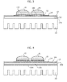
Figures 2 to 4 there is shown, as an example, a lighting device including an insulated metal substrate (IMS) comprisingelements Figures 2 and3 ) orelements Figure 4 ). - In the lighting device exemplified in
Figures 2 to 4 , the insulated metal substrate carries electrically conductive lines 14 (e.g. copper lines) and includes the metal base layer 12 (e.g. aluminium or copper), with one or more electrically powered light radiation sources 16 (e.g. LED sources). - In the lighting device exemplified in
Figures 2 to 4 , the thermally dissipative support (e.g. a housing or heatsink of a thermally conductive material, e.g. a metal as aluminium) carries the insulated metal substrate with the light radiation source(s) mounted on the electricallyconductive lines 14 through solder joints 18 (e.g. electrically conductive pastes or electrically conductive adhesives). - In the lighting device exemplified in
Figures 2 to 4 there is moreover provided a dielectric insulation, comprising a first electrically insulating layer interposed between the electricallyconductive lines 14 and thebase metal layer 12; this first insulating layer is denoted byreference 10 inFigures 2 and3 , and reference 10a inFigure 4 . - In one or more embodiments, features that are shown here separately by referring either to
Figures 2 and3 or toFigure 4 may be present in combination (see for exampleFigure 4 ). In the same way, such features may be present in a reversed way to what is shown here, e.g. with features shown inFigures 2 and/or 3 being applied to embodiments corresponding toFigure 4 , or with features shown inFigure 4 being applied to embodiments corresponding toFigures 2 and/or 3. In order to mention only one example among the various possibilities, we may refer tolayer 104, which will be better detailed by referring toFigure 4 . - In one or more embodiments, the first insulating layer may include, for example, at least one of:
- thermally-activated epoxy resin;
- glass-reinforced epoxy laminate sheet, such as for example FR4;
- epoxy-based insulation material with a thermally activating inorganic content filler, such as for example one or more of:
- aluminium nitride (AlN)
- alumina (Al2O3)
- boron nitride (BN)
- silicon nitride (Si3N4);
- a polyimide dielectric material with thermally conductive inorganic fillers;
- diamond-like carbon film, such as Thermeon™.
- One or more embodiments may envisage the implementation of a lighting device such as an insulated LED module with low thermal resistance by providing, in addition to the
first layer conductive lines 14 and saidmetal base layer 12, a second electrically insulating layer interposed betweenmetal base layer 12 andthermally dissipative support 20. - In one or more embodiments, said second insulating layer may include a
ceramic material coating 100 applied ontometal base layer 12. - In one or more embodiments,
ceramic material coating 100 may extend (only) on the backside of themetal base layer 12, i.e. betweenmetal base layer 12 andthermally dissipative support 20. - In one or more embodiments, as exemplified in
Figures 2 and3 , theceramic material coating 100 may extend both on the backside and on the lateral sides of the metal base layer 12 (and optionally of the first insulating layer 10).Figures 2 and3 exemplify therefore one or more embodiments wherein such aceramic coating 100 is applied to a PBA unit with an IMS-based insulation, by applying saidceramic coating 100 both on the back side (i.e. the side facing towards thermally dissipative support 20) ofmetal layer 12 and on the lateral sides thereof. - In one or more embodiments, as exemplified in
Figure 4 , theceramic material coating 100 may extend (only) on the lateral sides of the metal base layer (and optionally of the first insulating layer 10). - In one or more embodiments, as exemplified in
Figure 4 , on the backside ofmetal base layer 12, i.e. between themetal base layer 12 and thethermally dissipative support 20, the second insulatinglayer 10b may include a dielectric material similar to the material of the first insulatinglayer 10a, the second insulatinglayer 10b being thicker than the first insulatinglayer 10a. - As exemplified in
Figures 2 and3 , in one or more embodiments the second insulatinglayer 100 interposed between themetal base layer 12 and thethermally dissipative support 20 may be implemented as a ceramic-based coating applied on metal parts (e.g. aluminium), such as the backwall facing support 20 and/or the side walls of the PBA unit. - In one or more embodiments, such a ceramic material coating may be applied with different solutions on metal materials such as aluminium, of the type used in an IMS environment, e.g. wrought aluminium like 5052, 6082, 1050.
- For example, in one or more embodiments, such a ceramic-based material may be a dense insulation layer of aluminium oxide crystallites.
- In one or more embodiments, such a coating material may be obtained through a wet chemical process, e.g. as available from Cambridge Nanotherm of Haverhill (UK).
- In one or more embodiments, the dielectric thicknesses may range from 10 to 50 µm.
- In one or more embodiments, thermal conductivity may be up to 7 W/m.K.
- Another possibility is the use of an alumina layer.
- In one or more embodiment, such a coating material may be obtained via thermal spraying, wherein melted or heated materials are sprayed onto a surface to form a layer.
- In one or more embodiments, thicknesses may range e.g. from 50 to 500 µm.
- In one or more embodiments, thermal conductivity may be up to 22 W/m.K.
- Such a ceramic-based coating (e.g. applied on aluminium) is moreover adapted to improve the resistance to scratches of the PBA backside, with the opportunity to provide in addition a higher thermal conductivity with respect to traditional insulating foils.
- In one or more embodiments, in order to produce
dielectric layer 10 ultrathin layers with high thermal conductivity may be adopted (e.g. materials such as Bergquist HPL 38µm, 3W/m.K, available from Bergquist Company of Chanhassen, MN 55317 USA, or Aismalibar Cobritherm HTC Ultra-thin 35µm, 3.2W/m.K, available from Aismalibar of Barcelona (Spain). - In one or more embodiments, in the presence of a reduced thickness of
dielectric layer 10, the insulating properties are given mainly byceramic coating 100. - In one or more embodiments it is therefore possible to improve heat transfer from
light radiation sources 16 towardsmetal layer 12,layer 12 itself already acting as a heatsink, e.g. spreading the heat over its surface. The consequence is an improvement of the thermal conductivity towards thedissipative support 20. - In comparison with the application of insulating foils, the solution according to one or more presently exemplified embodiments may offer advantages such as:
- with approximately the same performance as for breakdown voltage (BDV), the thermal resistance Rth of
ceramic coating 100 may be lower (up to 1 order of magnitude less) than in insulating foils, - the production of the device is easier, because applying insulating foils may require additional manufacturing steps.
-
Figure 3 exemplifies one or more embodiments wherein there are provided one or more metal (e.g. copper) vias denoted by 102, which extend throughdielectric layer 10. - A corresponding technological solution is available for example from SinkPAD LLC di Placentia CA 92870, USA.
- The provision of such thermal vias from the
light radiation sources 16 towards themetal layer 12 of the IMS structure leads to an improvement of performances from a thermal point of view (with the possibility of lowering the soldering temperature) while achieving on the whole an electric insulation level similar to what can be obtained in one or more embodiments as exemplified inFigure 2 . - In one or more embodiments, as exemplified in
Figures 2 and3 ,ceramic coating 100 extends both on the bottom surface and on the lateral sides of the structure including metal material 12 (and dielectric layer 10). - One or more embodiments, as exemplified in
Figure 4 , may be seen as embodiments wherein the IMS dielectric layer denoted by 10 may so to say be split into two (sub)layers 10a and 10b. - In one or more embodiments, the
first layer 10a (arranged in the same position aslayer 10 of the former Figures, i.e. betweenmetal layer 12 andlight radiation sources 16 mounted on conductive lines 14) may be implemented as an ultra-thin layer with high thermal conductivity. (e.g. by using the previously-mentioned Bergquist and Aismalibar Cobritherm materials), so as to obtain a high thermal conductivity, without the need for that layer to perform an essential role in electric insulation. - In one or more embodiments,
second layer 10b (interposed betweenmetal layer 12 and heatsink 20) can play an important role in electric insulation, e.g. being adapted to be thicker thanlayer 10a while using the same amount of material. Therefore,Figure 4 exemplifies one or more embodiments adapted to be based on the principle of implementing the electric insulation mainly thanks to the second insulating layer, interposed betweenmetal base layer 12 andthermally dissipative support 20. - In one or more embodiments, as exemplified in
figure 4 , a ceramic coating 100 (e.g. as previously exemplified with reference toFigures 2 and3 ) may be present only on the sides of said structure including metal material 12 (and dielectric layer 10). - In one or more embodiments, as exemplified in
Figure 4 , the ceramic-based coating of Figure 100 on the sides of the PBA unit prevents lateral discharges frommetal layer 12 towardsheatsink 20. - In one or more embodiments the properties of thermal conductivity may be further enhanced thanks to a
layer 104 of an electrically and thermally conductive material (e.g. copper) extending betweenlayer 10b andheatsink 20, while keeping the general arrangement of the second electrically insulatinglayer 100; 10b interposed between themetal base material 12 and the thermally dissipative support (20). - Therefore, it will be appreciated that one or more embodiments:
- avoid a thickness increase of dielectric 10 or 10a interposed between
conductive lines 14 andbase metal 12, even enabling a decrease thereof, with the effect of reducing thermal resistance Rth and improving the ability to transfer heat fromsources 16 towardsbase metal 12; - do not require the use of high-performance dielectric materials;
- avoid the need of insulating foils between the PBA unit and the thermally dissipative support.
- Of course, without prejudice to the underlying principles of the invention, the details and the embodiments may vary, even appreciably, with respect to what has been described herein by way of non-limiting example only, without departing from the extent of protection. Said extent is defined by the annexed claims.
Claims (10)
- A lighting device, including:- an insulated metal substrate (10, 12, 14; 10a, 12, 14) carrying electrically conductive lines (14), the insulated metal substrate including a metal base layer (12),- at least one electrically powered light radiation source (16) mounted on the electrically conductive lines (14),- a thermally dissipative support (20) carrying the insulated metal substrate (10, 12, 14; 10a, 12, 14) with said at least one electrically powered light radiation source (16) mounted on the electrically conductive lines (14),- a first electrically insulating layer (10; 10a) interposed between said electrically conductive lines (14) and said base metal layer (12), and- a second electrically insulating layer (100; 10b) interposed between said base metal layer (12) and said thermally dissipative support (20),wherein said second electrically insulating layer (100) includes a ceramic material coating onto said base metal layer (12).
- The lighting device of claim 1, wherein said ceramic material coating extends between said base metal layer (12) and said thermally dissipative support (20).
- The lighting device of claim 1 or claim 2, wherein said ceramic material coating extends at the sides of said base metal layer (12) and, preferably, of said first electrically insulating layer (10; 10a).
- The lighting device of any of the previous claims, wherein said ceramic material coating is selected out of:- a layer of aluminium oxide crystallites, preferably with a thickness between 10 and 50 micron,- an alumina layer, preferably with a thickness between 50 and 500 micron.
- The lighting device of any of the previous claims, wherein said ceramic material coating is applied via one of a wet chemical process and thermal spraying.
- The lighting device of any of the previous claims, wherein at least one (10; 10a) of said first (10; 10a) and said second (10b) electrically insulating layers includes at least one of:- thermally-activated epoxy resin;- glass-reinforced epoxy laminate sheet material;- epoxy-based insulation material with thermally activating inorganic content filler, preferably selected as at least one of:- aluminium nitride (AlN)- alumina (Al2O3)- boron nitride (BN)- silicon nitride (Si3N4);- polyimide dielectric with thermally conductive inorganic filler;- diamond-like carbon film.
- The lighting device of any of the previous claims, wherein said second insulating layer (10b) is thicker than said first insulating layer (10a).
- The lighting device of any of the previous claims, including thermally conductive vias (102) through said first insulating layer (10).
- The lighting device of any of the previous claims, including a thermally conductive layer (104) between said second insulating layer (10b) and said thermally dissipative support (20).
- A method of producing a lighting device, including:- providing an insulated metal substrate (10, 12, 14; 10a, 12, 14) carrying electrically conductive lines (14), the insulated metal substrate including a metal base layer (12),- mounting at least one electrically powered light radiation source (16) on the electrically conductive lines (14),- providing a thermally dissipative support (20) carrying the insulated metal substrate (10, 12, 14; 10a, 12, 14) with said at least one electrically powered light radiation source (16) mounted on the electrically conductive lines (14),- providing a first electrically insulating layer (10; 10a) interposed between said electrically conductive lines (14) and said base metal layer (12) and a second electrically insulating layer (100; 10b) interposed between said base metal layer (12) and said thermally dissipative support (20), and- including in said second electrically insulating layer a ceramic material coating (100) onto said base metal layer (12).
Applications Claiming Priority (1)
| Application Number | Priority Date | Filing Date | Title |
|---|---|---|---|
| ITTO20140254 | 2014-03-27 |
Publications (2)
| Publication Number | Publication Date |
|---|---|
| EP2928272A1 true EP2928272A1 (en) | 2015-10-07 |
| EP2928272B1 EP2928272B1 (en) | 2016-09-21 |
Family
ID=50983000
Family Applications (1)
| Application Number | Title | Priority Date | Filing Date |
|---|---|---|---|
| EP15160245.5A Not-in-force EP2928272B1 (en) | 2014-03-27 | 2015-03-23 | A lighting device and corresponding method |
Country Status (1)
| Country | Link |
|---|---|
| EP (1) | EP2928272B1 (en) |
Cited By (1)
| Publication number | Priority date | Publication date | Assignee | Title |
|---|---|---|---|---|
| CN110831321A (en) * | 2019-10-30 | 2020-02-21 | 新鸿电子有限公司 | Multi-channel high-voltage power circuit and distributed X-ray source comprising same |
Citations (3)
| Publication number | Priority date | Publication date | Assignee | Title |
|---|---|---|---|---|
| DE102007046075A1 (en) * | 2007-09-26 | 2009-04-02 | Osram Opto Semiconductors Gmbh | LED module for lighting purpose and backlighting purpose, has printed circuit board with carrier from anodized aluminum, where conductors are attached on carrier and LED is arranged on carrier, and board stays in thermal contact with body |
| US20090225544A1 (en) * | 2005-06-07 | 2009-09-10 | Fujikura Ltd. | Enamel substrate for mounting light emitting elements, light emitting element module, illumination apparatus, display apparatus, and traffic signal |
| US20110316035A1 (en) * | 2010-06-23 | 2011-12-29 | Samsung Electro-Mechanics Co., Ltd. | Heat dissipating substrate and method of manufacturing the same |
-
2015
- 2015-03-23 EP EP15160245.5A patent/EP2928272B1/en not_active Not-in-force
Patent Citations (3)
| Publication number | Priority date | Publication date | Assignee | Title |
|---|---|---|---|---|
| US20090225544A1 (en) * | 2005-06-07 | 2009-09-10 | Fujikura Ltd. | Enamel substrate for mounting light emitting elements, light emitting element module, illumination apparatus, display apparatus, and traffic signal |
| DE102007046075A1 (en) * | 2007-09-26 | 2009-04-02 | Osram Opto Semiconductors Gmbh | LED module for lighting purpose and backlighting purpose, has printed circuit board with carrier from anodized aluminum, where conductors are attached on carrier and LED is arranged on carrier, and board stays in thermal contact with body |
| US20110316035A1 (en) * | 2010-06-23 | 2011-12-29 | Samsung Electro-Mechanics Co., Ltd. | Heat dissipating substrate and method of manufacturing the same |
Cited By (1)
| Publication number | Priority date | Publication date | Assignee | Title |
|---|---|---|---|---|
| CN110831321A (en) * | 2019-10-30 | 2020-02-21 | 新鸿电子有限公司 | Multi-channel high-voltage power circuit and distributed X-ray source comprising same |
Also Published As
| Publication number | Publication date |
|---|---|
| EP2928272B1 (en) | 2016-09-21 |
Similar Documents
| Publication | Publication Date | Title |
|---|---|---|
| US8011799B2 (en) | Thermal management of LED-based lighting systems | |
| EP2579692B1 (en) | Flexible circuit board | |
| US10524349B2 (en) | Printed circuit board with built-in vertical heat dissipation ceramic block, and electrical assembly comprising the board | |
| JP2011518436A (en) | Thermally conductive mounting elements for mounting printed circuit boards to heat sinks | |
| KR20080102300A (en) | LED integrated with thermal via | |
| CN102026496A (en) | Method for preparing printed circuit board with insulated micro radiator | |
| JP2012074703A (en) | Heat dissipation substrate, manufacturing method therefor, and light-emitting element package including the heat dissipation substrate | |
| US7875900B2 (en) | Thermally conductive structure of LED and manufacturing method thereof | |
| US20190355885A1 (en) | Resin composition for circuit board, and metal-base circuit board in which same is used | |
| KR101400305B1 (en) | Printed circuit board with graphene | |
| CN105744721B (en) | Circuit substrate | |
| US20150040388A1 (en) | Application of Dielectric Layer and Circuit Traces on Heat Sink | |
| EP2928272B1 (en) | A lighting device and corresponding method | |
| KR101064793B1 (en) | LED board | |
| TWI509194B (en) | Illumination apparatus | |
| JP2011192930A (en) | Substrate, method of manufacturing substrate, and lighting fixture | |
| CN1241157C (en) | Light-emitting diode display module with high heat dissipation | |
| CN203339214U (en) | A multi-ceramic-layer LED packaging structure | |
| CN103107275B (en) | Device for light emitting diode (LED) heat conduction and dissipation and insulation and voltage resistance | |
| KR101049887B1 (en) | Metal substrate structure for heat dissipation improvement and circuit protection of LED lighting equipment | |
| JP2011210948A (en) | Metal-base circuit board and method of manufacturing the same | |
| CN204894670U (en) | LED lamps and lanterns are with aluminium base two -sided copper -clad plate | |
| CN102870512A (en) | Mounting board heat dissipating laminate | |
| CN204289426U (en) | A kind of frequency converter IGBT radiator structure | |
| CN202511251U (en) | Heat conduction structure of LED lighting lamp |
Legal Events
| Date | Code | Title | Description |
|---|---|---|---|
| PUAI | Public reference made under article 153(3) epc to a published international application that has entered the european phase |
Free format text: ORIGINAL CODE: 0009012 |
|
| AK | Designated contracting states |
Kind code of ref document: A1 Designated state(s): AL AT BE BG CH CY CZ DE DK EE ES FI FR GB GR HR HU IE IS IT LI LT LU LV MC MK MT NL NO PL PT RO RS SE SI SK SM TR |
|
| AX | Request for extension of the european patent |
Extension state: BA ME |
|
| RAP1 | Party data changed (applicant data changed or rights of an application transferred) |
Owner name: OSRAM S.P.A. - SOCIETA' RIUNITE OSRAM EDISON CLERI Owner name: OSRAM GMBH |
|
| 17P | Request for examination filed |
Effective date: 20160208 |
|
| RBV | Designated contracting states (corrected) |
Designated state(s): AL AT BE BG CH CY CZ DE DK EE ES FI FR GB GR HR HU IE IS IT LI LT LU LV MC MK MT NL NO PL PT RO RS SE SI SK SM TR |
|
| RIC1 | Information provided on ipc code assigned before grant |
Ipc: H05K 3/00 20060101ALI20160304BHEP Ipc: H05K 1/02 20060101ALN20160304BHEP Ipc: H05K 1/05 20060101AFI20160304BHEP |
|
| GRAP | Despatch of communication of intention to grant a patent |
Free format text: ORIGINAL CODE: EPIDOSNIGR1 |
|
| INTG | Intention to grant announced |
Effective date: 20160504 |
|
| GRAS | Grant fee paid |
Free format text: ORIGINAL CODE: EPIDOSNIGR3 |
|
| GRAA | (expected) grant |
Free format text: ORIGINAL CODE: 0009210 |
|
| AK | Designated contracting states |
Kind code of ref document: B1 Designated state(s): AL AT BE BG CH CY CZ DE DK EE ES FI FR GB GR HR HU IE IS IT LI LT LU LV MC MK MT NL NO PL PT RO RS SE SI SK SM TR |
|
| REG | Reference to a national code |
Ref country code: GB Ref legal event code: FG4D |
|
| REG | Reference to a national code |
Ref country code: CH Ref legal event code: EP |
|
| REG | Reference to a national code |
Ref country code: AT Ref legal event code: REF Ref document number: 831959 Country of ref document: AT Kind code of ref document: T Effective date: 20161015 |
|
| REG | Reference to a national code |
Ref country code: IE Ref legal event code: FG4D |
|
| REG | Reference to a national code |
Ref country code: DE Ref legal event code: R096 Ref document number: 602015000354 Country of ref document: DE |
|
| REG | Reference to a national code |
Ref country code: LT Ref legal event code: MG4D Ref country code: NL Ref legal event code: MP Effective date: 20160921 |
|
| PG25 | Lapsed in a contracting state [announced via postgrant information from national office to epo] |
Ref country code: LT Free format text: LAPSE BECAUSE OF FAILURE TO SUBMIT A TRANSLATION OF THE DESCRIPTION OR TO PAY THE FEE WITHIN THE PRESCRIBED TIME-LIMIT Effective date: 20160921 Ref country code: NO Free format text: LAPSE BECAUSE OF FAILURE TO SUBMIT A TRANSLATION OF THE DESCRIPTION OR TO PAY THE FEE WITHIN THE PRESCRIBED TIME-LIMIT Effective date: 20161221 Ref country code: FI Free format text: LAPSE BECAUSE OF FAILURE TO SUBMIT A TRANSLATION OF THE DESCRIPTION OR TO PAY THE FEE WITHIN THE PRESCRIBED TIME-LIMIT Effective date: 20160921 Ref country code: RS Free format text: LAPSE BECAUSE OF FAILURE TO SUBMIT A TRANSLATION OF THE DESCRIPTION OR TO PAY THE FEE WITHIN THE PRESCRIBED TIME-LIMIT Effective date: 20160921 |
|
| REG | Reference to a national code |
Ref country code: AT Ref legal event code: MK05 Ref document number: 831959 Country of ref document: AT Kind code of ref document: T Effective date: 20160921 |
|
| PG25 | Lapsed in a contracting state [announced via postgrant information from national office to epo] |
Ref country code: SE Free format text: LAPSE BECAUSE OF FAILURE TO SUBMIT A TRANSLATION OF THE DESCRIPTION OR TO PAY THE FEE WITHIN THE PRESCRIBED TIME-LIMIT Effective date: 20160921 Ref country code: LV Free format text: LAPSE BECAUSE OF FAILURE TO SUBMIT A TRANSLATION OF THE DESCRIPTION OR TO PAY THE FEE WITHIN THE PRESCRIBED TIME-LIMIT Effective date: 20160921 Ref country code: NL Free format text: LAPSE BECAUSE OF FAILURE TO SUBMIT A TRANSLATION OF THE DESCRIPTION OR TO PAY THE FEE WITHIN THE PRESCRIBED TIME-LIMIT Effective date: 20160921 Ref country code: GR Free format text: LAPSE BECAUSE OF FAILURE TO SUBMIT A TRANSLATION OF THE DESCRIPTION OR TO PAY THE FEE WITHIN THE PRESCRIBED TIME-LIMIT Effective date: 20161222 |
|
| REG | Reference to a national code |
Ref country code: FR Ref legal event code: PLFP Year of fee payment: 3 |
|
| PG25 | Lapsed in a contracting state [announced via postgrant information from national office to epo] |
Ref country code: RO Free format text: LAPSE BECAUSE OF FAILURE TO SUBMIT A TRANSLATION OF THE DESCRIPTION OR TO PAY THE FEE WITHIN THE PRESCRIBED TIME-LIMIT Effective date: 20160921 Ref country code: EE Free format text: LAPSE BECAUSE OF FAILURE TO SUBMIT A TRANSLATION OF THE DESCRIPTION OR TO PAY THE FEE WITHIN THE PRESCRIBED TIME-LIMIT Effective date: 20160921 |
|
| PG25 | Lapsed in a contracting state [announced via postgrant information from national office to epo] |
Ref country code: BG Free format text: LAPSE BECAUSE OF FAILURE TO SUBMIT A TRANSLATION OF THE DESCRIPTION OR TO PAY THE FEE WITHIN THE PRESCRIBED TIME-LIMIT Effective date: 20161221 Ref country code: SK Free format text: LAPSE BECAUSE OF FAILURE TO SUBMIT A TRANSLATION OF THE DESCRIPTION OR TO PAY THE FEE WITHIN THE PRESCRIBED TIME-LIMIT Effective date: 20160921 Ref country code: BE Free format text: LAPSE BECAUSE OF FAILURE TO SUBMIT A TRANSLATION OF THE DESCRIPTION OR TO PAY THE FEE WITHIN THE PRESCRIBED TIME-LIMIT Effective date: 20160921 Ref country code: CZ Free format text: LAPSE BECAUSE OF FAILURE TO SUBMIT A TRANSLATION OF THE DESCRIPTION OR TO PAY THE FEE WITHIN THE PRESCRIBED TIME-LIMIT Effective date: 20160921 Ref country code: AT Free format text: LAPSE BECAUSE OF FAILURE TO SUBMIT A TRANSLATION OF THE DESCRIPTION OR TO PAY THE FEE WITHIN THE PRESCRIBED TIME-LIMIT Effective date: 20160921 Ref country code: SM Free format text: LAPSE BECAUSE OF FAILURE TO SUBMIT A TRANSLATION OF THE DESCRIPTION OR TO PAY THE FEE WITHIN THE PRESCRIBED TIME-LIMIT Effective date: 20160921 Ref country code: ES Free format text: LAPSE BECAUSE OF FAILURE TO SUBMIT A TRANSLATION OF THE DESCRIPTION OR TO PAY THE FEE WITHIN THE PRESCRIBED TIME-LIMIT Effective date: 20160921 Ref country code: PT Free format text: LAPSE BECAUSE OF FAILURE TO SUBMIT A TRANSLATION OF THE DESCRIPTION OR TO PAY THE FEE WITHIN THE PRESCRIBED TIME-LIMIT Effective date: 20170123 Ref country code: PL Free format text: LAPSE BECAUSE OF FAILURE TO SUBMIT A TRANSLATION OF THE DESCRIPTION OR TO PAY THE FEE WITHIN THE PRESCRIBED TIME-LIMIT Effective date: 20160921 Ref country code: IS Free format text: LAPSE BECAUSE OF FAILURE TO SUBMIT A TRANSLATION OF THE DESCRIPTION OR TO PAY THE FEE WITHIN THE PRESCRIBED TIME-LIMIT Effective date: 20170121 |
|
| REG | Reference to a national code |
Ref country code: DE Ref legal event code: R097 Ref document number: 602015000354 Country of ref document: DE |
|
| PG25 | Lapsed in a contracting state [announced via postgrant information from national office to epo] |
Ref country code: IT Free format text: LAPSE BECAUSE OF FAILURE TO SUBMIT A TRANSLATION OF THE DESCRIPTION OR TO PAY THE FEE WITHIN THE PRESCRIBED TIME-LIMIT Effective date: 20160921 |
|
| PLBE | No opposition filed within time limit |
Free format text: ORIGINAL CODE: 0009261 |
|
| STAA | Information on the status of an ep patent application or granted ep patent |
Free format text: STATUS: NO OPPOSITION FILED WITHIN TIME LIMIT |
|
| PG25 | Lapsed in a contracting state [announced via postgrant information from national office to epo] |
Ref country code: DK Free format text: LAPSE BECAUSE OF FAILURE TO SUBMIT A TRANSLATION OF THE DESCRIPTION OR TO PAY THE FEE WITHIN THE PRESCRIBED TIME-LIMIT Effective date: 20160921 |
|
| 26N | No opposition filed |
Effective date: 20170622 |
|
| PG25 | Lapsed in a contracting state [announced via postgrant information from national office to epo] |
Ref country code: SI Free format text: LAPSE BECAUSE OF FAILURE TO SUBMIT A TRANSLATION OF THE DESCRIPTION OR TO PAY THE FEE WITHIN THE PRESCRIBED TIME-LIMIT Effective date: 20160921 Ref country code: MC Free format text: LAPSE BECAUSE OF FAILURE TO SUBMIT A TRANSLATION OF THE DESCRIPTION OR TO PAY THE FEE WITHIN THE PRESCRIBED TIME-LIMIT Effective date: 20160921 |
|
| REG | Reference to a national code |
Ref country code: IE Ref legal event code: MM4A |
|
| PG25 | Lapsed in a contracting state [announced via postgrant information from national office to epo] |
Ref country code: LU Free format text: LAPSE BECAUSE OF NON-PAYMENT OF DUE FEES Effective date: 20170323 |
|
| PG25 | Lapsed in a contracting state [announced via postgrant information from national office to epo] |
Ref country code: IE Free format text: LAPSE BECAUSE OF NON-PAYMENT OF DUE FEES Effective date: 20170323 |
|
| REG | Reference to a national code |
Ref country code: FR Ref legal event code: PLFP Year of fee payment: 4 |
|
| PG25 | Lapsed in a contracting state [announced via postgrant information from national office to epo] |
Ref country code: MT Free format text: LAPSE BECAUSE OF NON-PAYMENT OF DUE FEES Effective date: 20170323 |
|
| PG25 | Lapsed in a contracting state [announced via postgrant information from national office to epo] |
Ref country code: AL Free format text: LAPSE BECAUSE OF FAILURE TO SUBMIT A TRANSLATION OF THE DESCRIPTION OR TO PAY THE FEE WITHIN THE PRESCRIBED TIME-LIMIT Effective date: 20160921 |
|
| REG | Reference to a national code |
Ref country code: CH Ref legal event code: PL |
|
| PG25 | Lapsed in a contracting state [announced via postgrant information from national office to epo] |
Ref country code: LI Free format text: LAPSE BECAUSE OF NON-PAYMENT OF DUE FEES Effective date: 20180331 Ref country code: CH Free format text: LAPSE BECAUSE OF NON-PAYMENT OF DUE FEES Effective date: 20180331 |
|
| PGFP | Annual fee paid to national office [announced via postgrant information from national office to epo] |
Ref country code: FR Payment date: 20190320 Year of fee payment: 5 Ref country code: GB Payment date: 20190320 Year of fee payment: 5 |
|
| PG25 | Lapsed in a contracting state [announced via postgrant information from national office to epo] |
Ref country code: HU Free format text: LAPSE BECAUSE OF FAILURE TO SUBMIT A TRANSLATION OF THE DESCRIPTION OR TO PAY THE FEE WITHIN THE PRESCRIBED TIME-LIMIT; INVALID AB INITIO Effective date: 20150323 |
|
| PG25 | Lapsed in a contracting state [announced via postgrant information from national office to epo] |
Ref country code: CY Free format text: LAPSE BECAUSE OF FAILURE TO SUBMIT A TRANSLATION OF THE DESCRIPTION OR TO PAY THE FEE WITHIN THE PRESCRIBED TIME-LIMIT Effective date: 20160921 |
|
| PG25 | Lapsed in a contracting state [announced via postgrant information from national office to epo] |
Ref country code: MK Free format text: LAPSE BECAUSE OF FAILURE TO SUBMIT A TRANSLATION OF THE DESCRIPTION OR TO PAY THE FEE WITHIN THE PRESCRIBED TIME-LIMIT Effective date: 20160921 |
|
| PG25 | Lapsed in a contracting state [announced via postgrant information from national office to epo] |
Ref country code: TR Free format text: LAPSE BECAUSE OF FAILURE TO SUBMIT A TRANSLATION OF THE DESCRIPTION OR TO PAY THE FEE WITHIN THE PRESCRIBED TIME-LIMIT Effective date: 20160921 |
|
| PG25 | Lapsed in a contracting state [announced via postgrant information from national office to epo] |
Ref country code: HR Free format text: LAPSE BECAUSE OF FAILURE TO SUBMIT A TRANSLATION OF THE DESCRIPTION OR TO PAY THE FEE WITHIN THE PRESCRIBED TIME-LIMIT Effective date: 20160921 |
|
| GBPC | Gb: european patent ceased through non-payment of renewal fee |
Effective date: 20200323 |
|
| PG25 | Lapsed in a contracting state [announced via postgrant information from national office to epo] |
Ref country code: GB Free format text: LAPSE BECAUSE OF NON-PAYMENT OF DUE FEES Effective date: 20200323 |
|
| PGFP | Annual fee paid to national office [announced via postgrant information from national office to epo] |
Ref country code: DE Payment date: 20220322 Year of fee payment: 8 |
|
| PG25 | Lapsed in a contracting state [announced via postgrant information from national office to epo] |
Ref country code: FR Free format text: LAPSE BECAUSE OF NON-PAYMENT OF DUE FEES Effective date: 20200331 |
|
| P01 | Opt-out of the competence of the unified patent court (upc) registered |
Effective date: 20230821 |
|
| REG | Reference to a national code |
Ref country code: DE Ref legal event code: R119 Ref document number: 602015000354 Country of ref document: DE |
|
| PG25 | Lapsed in a contracting state [announced via postgrant information from national office to epo] |
Ref country code: DE Free format text: LAPSE BECAUSE OF NON-PAYMENT OF DUE FEES Effective date: 20231003 |