EP2928264B1 - Heating element and method for manufacturing same - Google Patents
Heating element and method for manufacturing same Download PDFInfo
- Publication number
- EP2928264B1 EP2928264B1 EP14754485.2A EP14754485A EP2928264B1 EP 2928264 B1 EP2928264 B1 EP 2928264B1 EP 14754485 A EP14754485 A EP 14754485A EP 2928264 B1 EP2928264 B1 EP 2928264B1
- Authority
- EP
- European Patent Office
- Prior art keywords
- conductive
- heating
- pattern
- heating element
- area
- Prior art date
- Legal status (The legal status is an assumption and is not a legal conclusion. Google has not performed a legal analysis and makes no representation as to the accuracy of the status listed.)
- Active
Links
- 238000010438 heat treatment Methods 0.000 title claims description 286
- 238000000034 method Methods 0.000 title claims description 84
- 238000004519 manufacturing process Methods 0.000 title description 2
- 239000000758 substrate Substances 0.000 claims description 54
- 239000010410 layer Substances 0.000 claims description 51
- 239000000463 material Substances 0.000 claims description 40
- 229910052751 metal Inorganic materials 0.000 claims description 22
- 239000002184 metal Substances 0.000 claims description 22
- PXHVJJICTQNCMI-UHFFFAOYSA-N Nickel Chemical compound [Ni] PXHVJJICTQNCMI-UHFFFAOYSA-N 0.000 claims description 19
- RYGMFSIKBFXOCR-UHFFFAOYSA-N Copper Chemical compound [Cu] RYGMFSIKBFXOCR-UHFFFAOYSA-N 0.000 claims description 18
- 239000010949 copper Substances 0.000 claims description 16
- BASFCYQUMIYNBI-UHFFFAOYSA-N platinum Chemical compound [Pt] BASFCYQUMIYNBI-UHFFFAOYSA-N 0.000 claims description 16
- 229910052802 copper Inorganic materials 0.000 claims description 15
- 229910052709 silver Inorganic materials 0.000 claims description 15
- 239000004332 silver Substances 0.000 claims description 14
- BQCADISMDOOEFD-UHFFFAOYSA-N Silver Chemical compound [Ag] BQCADISMDOOEFD-UHFFFAOYSA-N 0.000 claims description 12
- 239000012790 adhesive layer Substances 0.000 claims description 12
- 229910052759 nickel Inorganic materials 0.000 claims description 10
- 229910052782 aluminium Inorganic materials 0.000 claims description 9
- XAGFODPZIPBFFR-UHFFFAOYSA-N aluminium Chemical compound [Al] XAGFODPZIPBFFR-UHFFFAOYSA-N 0.000 claims description 8
- 229910052804 chromium Inorganic materials 0.000 claims description 8
- 239000011651 chromium Substances 0.000 claims description 8
- 229910052750 molybdenum Inorganic materials 0.000 claims description 8
- 229910052697 platinum Inorganic materials 0.000 claims description 8
- 239000010936 titanium Substances 0.000 claims description 8
- 229910052719 titanium Inorganic materials 0.000 claims description 8
- VYZAMTAEIAYCRO-UHFFFAOYSA-N Chromium Chemical compound [Cr] VYZAMTAEIAYCRO-UHFFFAOYSA-N 0.000 claims description 7
- ZOKXTWBITQBERF-UHFFFAOYSA-N Molybdenum Chemical compound [Mo] ZOKXTWBITQBERF-UHFFFAOYSA-N 0.000 claims description 7
- RTAQQCXQSZGOHL-UHFFFAOYSA-N Titanium Chemical compound [Ti] RTAQQCXQSZGOHL-UHFFFAOYSA-N 0.000 claims description 7
- 229910045601 alloy Inorganic materials 0.000 claims description 7
- 239000000956 alloy Substances 0.000 claims description 7
- 239000011733 molybdenum Substances 0.000 claims description 7
- NIXOWILDQLNWCW-UHFFFAOYSA-M Acrylate Chemical compound [O-]C(=O)C=C NIXOWILDQLNWCW-UHFFFAOYSA-M 0.000 claims description 2
- JOYRKODLDBILNP-UHFFFAOYSA-N Ethyl urethane Chemical compound CCOC(N)=O JOYRKODLDBILNP-UHFFFAOYSA-N 0.000 claims description 2
- 229920001940 conductive polymer Polymers 0.000 claims description 2
- 239000002923 metal particle Substances 0.000 claims description 2
- 239000002210 silicon-based material Substances 0.000 claims description 2
- 239000011521 glass Substances 0.000 description 26
- 239000004973 liquid crystal related substance Substances 0.000 description 22
- 238000010586 diagram Methods 0.000 description 20
- 239000010408 film Substances 0.000 description 19
- 238000007639 printing Methods 0.000 description 13
- 238000009826 distribution Methods 0.000 description 11
- 238000005530 etching Methods 0.000 description 11
- 230000000694 effects Effects 0.000 description 10
- 230000001788 irregular Effects 0.000 description 10
- 239000004020 conductor Substances 0.000 description 9
- 238000000206 photolithography Methods 0.000 description 8
- 239000002313 adhesive film Substances 0.000 description 7
- 238000010304 firing Methods 0.000 description 7
- 238000007645 offset printing Methods 0.000 description 6
- 239000011230 binding agent Substances 0.000 description 5
- 229920002120 photoresistant polymer Polymers 0.000 description 5
- 239000004033 plastic Substances 0.000 description 5
- 229920003023 plastic Polymers 0.000 description 5
- 238000007747 plating Methods 0.000 description 5
- 239000000047 product Substances 0.000 description 5
- 238000004544 sputter deposition Methods 0.000 description 5
- 239000010409 thin film Substances 0.000 description 5
- OKTJSMMVPCPJKN-UHFFFAOYSA-N Carbon Chemical compound [C] OKTJSMMVPCPJKN-UHFFFAOYSA-N 0.000 description 4
- 239000000853 adhesive Substances 0.000 description 4
- 230000001070 adhesive effect Effects 0.000 description 4
- 239000011889 copper foil Substances 0.000 description 4
- 210000002858 crystal cell Anatomy 0.000 description 4
- 238000011049 filling Methods 0.000 description 4
- 238000007650 screen-printing Methods 0.000 description 4
- -1 silver halide Chemical class 0.000 description 4
- 239000002904 solvent Substances 0.000 description 4
- 229910021393 carbon nanotube Inorganic materials 0.000 description 3
- 239000002041 carbon nanotube Substances 0.000 description 3
- 239000011248 coating agent Substances 0.000 description 3
- 238000000576 coating method Methods 0.000 description 3
- 230000000052 comparative effect Effects 0.000 description 3
- 238000000151 deposition Methods 0.000 description 3
- 238000005240 physical vapour deposition Methods 0.000 description 3
- 239000002985 plastic film Substances 0.000 description 3
- 229920006255 plastic film Polymers 0.000 description 3
- 229920002037 poly(vinyl butyral) polymer Polymers 0.000 description 3
- 229920000139 polyethylene terephthalate Polymers 0.000 description 3
- 239000005020 polyethylene terephthalate Substances 0.000 description 3
- 229920006254 polymer film Polymers 0.000 description 3
- 238000002834 transmittance Methods 0.000 description 3
- 229920002160 Celluloid Polymers 0.000 description 2
- 125000000218 acetic acid group Chemical group C(C)(=O)* 0.000 description 2
- 238000005229 chemical vapour deposition Methods 0.000 description 2
- 239000000470 constituent Substances 0.000 description 2
- 238000002474 experimental method Methods 0.000 description 2
- 238000007646 gravure printing Methods 0.000 description 2
- 239000002245 particle Substances 0.000 description 2
- 239000011112 polyethylene naphthalate Substances 0.000 description 2
- 230000001681 protective effect Effects 0.000 description 2
- 238000007740 vapor deposition Methods 0.000 description 2
- 230000000007 visual effect Effects 0.000 description 2
- VXQBJTKSVGFQOL-UHFFFAOYSA-N 2-(2-butoxyethoxy)ethyl acetate Chemical compound CCCCOCCOCCOC(C)=O VXQBJTKSVGFQOL-UHFFFAOYSA-N 0.000 description 1
- FPZWZCWUIYYYBU-UHFFFAOYSA-N 2-(2-ethoxyethoxy)ethyl acetate Chemical compound CCOCCOCCOC(C)=O FPZWZCWUIYYYBU-UHFFFAOYSA-N 0.000 description 1
- SVONRAPFKPVNKG-UHFFFAOYSA-N 2-ethoxyethyl acetate Chemical compound CCOCCOC(C)=O SVONRAPFKPVNKG-UHFFFAOYSA-N 0.000 description 1
- 239000004925 Acrylic resin Substances 0.000 description 1
- 229920002799 BoPET Polymers 0.000 description 1
- 239000004593 Epoxy Substances 0.000 description 1
- 229920012266 Poly(ether sulfone) PES Polymers 0.000 description 1
- WUOACPNHFRMFPN-UHFFFAOYSA-N alpha-terpineol Chemical compound CC1=CCC(C(C)(C)O)CC1 WUOACPNHFRMFPN-UHFFFAOYSA-N 0.000 description 1
- 230000015572 biosynthetic process Effects 0.000 description 1
- 230000000903 blocking effect Effects 0.000 description 1
- 229910052799 carbon Inorganic materials 0.000 description 1
- 239000012461 cellulose resin Substances 0.000 description 1
- 238000004140 cleaning Methods 0.000 description 1
- 229910000428 cobalt oxide Inorganic materials 0.000 description 1
- IVMYJDGYRUAWML-UHFFFAOYSA-N cobalt(ii) oxide Chemical compound [Co]=O IVMYJDGYRUAWML-UHFFFAOYSA-N 0.000 description 1
- 239000003086 colorant Substances 0.000 description 1
- 239000013065 commercial product Substances 0.000 description 1
- 238000009833 condensation Methods 0.000 description 1
- 230000005494 condensation Effects 0.000 description 1
- JHIVVAPYMSGYDF-UHFFFAOYSA-N cyclohexanone Chemical compound O=C1CCCCC1 JHIVVAPYMSGYDF-UHFFFAOYSA-N 0.000 description 1
- SQIFACVGCPWBQZ-UHFFFAOYSA-N delta-terpineol Natural products CC(C)(O)C1CCC(=C)CC1 SQIFACVGCPWBQZ-UHFFFAOYSA-N 0.000 description 1
- 230000006866 deterioration Effects 0.000 description 1
- 208000002173 dizziness Diseases 0.000 description 1
- 230000005611 electricity Effects 0.000 description 1
- 239000007772 electrode material Substances 0.000 description 1
- 238000007772 electroless plating Methods 0.000 description 1
- 238000010894 electron beam technology Methods 0.000 description 1
- 229910052737 gold Inorganic materials 0.000 description 1
- 239000010931 gold Substances 0.000 description 1
- AMGQUBHHOARCQH-UHFFFAOYSA-N indium;oxotin Chemical compound [In].[Sn]=O AMGQUBHHOARCQH-UHFFFAOYSA-N 0.000 description 1
- 238000009413 insulation Methods 0.000 description 1
- 238000010030 laminating Methods 0.000 description 1
- 150000002739 metals Chemical class 0.000 description 1
- 238000002156 mixing Methods 0.000 description 1
- 230000003287 optical effect Effects 0.000 description 1
- 238000000059 patterning Methods 0.000 description 1
- 229920003207 poly(ethylene-2,6-naphthalate) Polymers 0.000 description 1
- 229920000515 polycarbonate Polymers 0.000 description 1
- 239000004417 polycarbonate Substances 0.000 description 1
- 229920005668 polycarbonate resin Polymers 0.000 description 1
- 239000004431 polycarbonate resin Substances 0.000 description 1
- 229920001225 polyester resin Polymers 0.000 description 1
- 239000004645 polyester resin Substances 0.000 description 1
- 229920001721 polyimide Polymers 0.000 description 1
- 239000009719 polyimide resin Substances 0.000 description 1
- 229920005672 polyolefin resin Polymers 0.000 description 1
- 239000004814 polyurethane Substances 0.000 description 1
- 229920005749 polyurethane resin Polymers 0.000 description 1
- 238000003825 pressing Methods 0.000 description 1
- 230000003578 releasing effect Effects 0.000 description 1
- 230000003252 repetitive effect Effects 0.000 description 1
- 229920005989 resin Polymers 0.000 description 1
- 239000011347 resin Substances 0.000 description 1
- 238000005096 rolling process Methods 0.000 description 1
- 229920002379 silicone rubber Polymers 0.000 description 1
- 239000010944 silver (metal) Substances 0.000 description 1
- ADZWSOLPGZMUMY-UHFFFAOYSA-M silver bromide Chemical compound [Ag]Br ADZWSOLPGZMUMY-UHFFFAOYSA-M 0.000 description 1
- 238000010583 slow cooling Methods 0.000 description 1
- 238000005476 soldering Methods 0.000 description 1
- 238000003980 solgel method Methods 0.000 description 1
- 230000001360 synchronised effect Effects 0.000 description 1
- 229940116411 terpineol Drugs 0.000 description 1
Images


Classifications
-
- H—ELECTRICITY
- H05—ELECTRIC TECHNIQUES NOT OTHERWISE PROVIDED FOR
- H05B—ELECTRIC HEATING; ELECTRIC LIGHT SOURCES NOT OTHERWISE PROVIDED FOR; CIRCUIT ARRANGEMENTS FOR ELECTRIC LIGHT SOURCES, IN GENERAL
- H05B3/00—Ohmic-resistance heating
- H05B3/84—Heating arrangements specially adapted for transparent or reflecting areas, e.g. for demisting or de-icing windows, mirrors or vehicle windshields
- H05B3/86—Heating arrangements specially adapted for transparent or reflecting areas, e.g. for demisting or de-icing windows, mirrors or vehicle windshields the heating conductors being embedded in the transparent or reflecting material
-
- H—ELECTRICITY
- H01—ELECTRIC ELEMENTS
- H01C—RESISTORS
- H01C17/00—Apparatus or processes specially adapted for manufacturing resistors
-
- H—ELECTRICITY
- H01—ELECTRIC ELEMENTS
- H01C—RESISTORS
- H01C17/00—Apparatus or processes specially adapted for manufacturing resistors
- H01C17/28—Apparatus or processes specially adapted for manufacturing resistors adapted for applying terminals
-
- H—ELECTRICITY
- H05—ELECTRIC TECHNIQUES NOT OTHERWISE PROVIDED FOR
- H05B—ELECTRIC HEATING; ELECTRIC LIGHT SOURCES NOT OTHERWISE PROVIDED FOR; CIRCUIT ARRANGEMENTS FOR ELECTRIC LIGHT SOURCES, IN GENERAL
- H05B1/00—Details of electric heating devices
- H05B1/02—Automatic switching arrangements specially adapted to apparatus ; Control of heating devices
- H05B1/0227—Applications
- H05B1/023—Industrial applications
- H05B1/0236—Industrial applications for vehicles
-
- H—ELECTRICITY
- H05—ELECTRIC TECHNIQUES NOT OTHERWISE PROVIDED FOR
- H05B—ELECTRIC HEATING; ELECTRIC LIGHT SOURCES NOT OTHERWISE PROVIDED FOR; CIRCUIT ARRANGEMENTS FOR ELECTRIC LIGHT SOURCES, IN GENERAL
- H05B3/00—Ohmic-resistance heating
- H05B3/20—Heating elements having extended surface area substantially in a two-dimensional plane, e.g. plate-heater
- H05B3/22—Heating elements having extended surface area substantially in a two-dimensional plane, e.g. plate-heater non-flexible
- H05B3/28—Heating elements having extended surface area substantially in a two-dimensional plane, e.g. plate-heater non-flexible heating conductor embedded in insulating material
- H05B3/286—Heating elements having extended surface area substantially in a two-dimensional plane, e.g. plate-heater non-flexible heating conductor embedded in insulating material the insulating material being an organic material, e.g. plastic
-
- H—ELECTRICITY
- H05—ELECTRIC TECHNIQUES NOT OTHERWISE PROVIDED FOR
- H05B—ELECTRIC HEATING; ELECTRIC LIGHT SOURCES NOT OTHERWISE PROVIDED FOR; CIRCUIT ARRANGEMENTS FOR ELECTRIC LIGHT SOURCES, IN GENERAL
- H05B3/00—Ohmic-resistance heating
- H05B3/84—Heating arrangements specially adapted for transparent or reflecting areas, e.g. for demisting or de-icing windows, mirrors or vehicle windshields
-
- H—ELECTRICITY
- H05—ELECTRIC TECHNIQUES NOT OTHERWISE PROVIDED FOR
- H05B—ELECTRIC HEATING; ELECTRIC LIGHT SOURCES NOT OTHERWISE PROVIDED FOR; CIRCUIT ARRANGEMENTS FOR ELECTRIC LIGHT SOURCES, IN GENERAL
- H05B2203/00—Aspects relating to Ohmic resistive heating covered by group H05B3/00
- H05B2203/002—Heaters using a particular layout for the resistive material or resistive elements
-
- H—ELECTRICITY
- H05—ELECTRIC TECHNIQUES NOT OTHERWISE PROVIDED FOR
- H05B—ELECTRIC HEATING; ELECTRIC LIGHT SOURCES NOT OTHERWISE PROVIDED FOR; CIRCUIT ARRANGEMENTS FOR ELECTRIC LIGHT SOURCES, IN GENERAL
- H05B2203/00—Aspects relating to Ohmic resistive heating covered by group H05B3/00
- H05B2203/011—Heaters using laterally extending conductive material as connecting means
-
- H—ELECTRICITY
- H05—ELECTRIC TECHNIQUES NOT OTHERWISE PROVIDED FOR
- H05B—ELECTRIC HEATING; ELECTRIC LIGHT SOURCES NOT OTHERWISE PROVIDED FOR; CIRCUIT ARRANGEMENTS FOR ELECTRIC LIGHT SOURCES, IN GENERAL
- H05B2203/00—Aspects relating to Ohmic resistive heating covered by group H05B3/00
- H05B2203/013—Heaters using resistive films or coatings
-
- Y—GENERAL TAGGING OF NEW TECHNOLOGICAL DEVELOPMENTS; GENERAL TAGGING OF CROSS-SECTIONAL TECHNOLOGIES SPANNING OVER SEVERAL SECTIONS OF THE IPC; TECHNICAL SUBJECTS COVERED BY FORMER USPC CROSS-REFERENCE ART COLLECTIONS [XRACs] AND DIGESTS
- Y10—TECHNICAL SUBJECTS COVERED BY FORMER USPC
- Y10T—TECHNICAL SUBJECTS COVERED BY FORMER US CLASSIFICATION
- Y10T29/00—Metal working
- Y10T29/49—Method of mechanical manufacture
- Y10T29/49002—Electrical device making
- Y10T29/49082—Resistor making
- Y10T29/49085—Thermally variable
Definitions
- the present application relates to a heating element and a method for preparing the same.
- the heating glass uses a concept that heat is generated from a heating wire by applying electricity to both terminals of the heating wire after attaching a heating wire sheet onto a glass surface or directly forming the heating wire on the glass surface and a temperature of the glass surface is increased by the generated heat.
- an amount of current needs to be increased.
- a kind of busbar which may supply the current to the metal wire a kind of and a forming method of the busbar must be selected for simultaneously controlling the heat generated in the busbar and the heat generated due to a contact resistance of the busbar and a transparent heating part.
- the contact with the busbar is a very important problem due to the small line width and a line height of the metal wire.
- An object of the present invention is to provide a heating element and a method for preparing the same that may prevent a resistance value between busbars of the heating element from being increased or local heat in a heating pattern from being generated.
- An exemplary embodiment of the present invention provides a heating element according to claim 1.
- Another exemplary embodiment of the present invention provides a method of preparing a heating element according to claim 13.
- yet another exemplary embodiment of the present invention provides a heating element for a vehicle or architecture including the heating element.
- Still another exemplary embodiment of the present invention provides a display device including the heating element.
- the exemplary embodiment of the present invention it is possible to prevent local heat between the heating element and the busbar from being generated by positioning the busbar on a conductive layer area to control a contact resistance between the heating element and the busbar.
- a heating pattern is formed by a method of etching a portion except for a pattern after coating a metal thin film of 1 ⁇ m or more on a polymer film and forming the pattern with an etching resist by a photolithography method or a printing method.
- the contact portion of the heating pattern and the busbar is limited and thus a phenomenon in which a resistance value between the busbars increases may occur, and a phenomenon in which the local heat in the heating pattern is generated may occur.
- the heating element according to the present invention includes a substrate, a conductive heating unit provided on the substrate, and two busbars provided to apply respective voltages to both ends of the conductive heating unit, in which the conductive heating unit includes a conductive heating pattern area and two conductive layer areas provided at both ends of the conductive heating pattern area, and the two busbars are provided on the conductive layer areas, respectively.
- the two conductive layer areas provided at both ends of the conductive heating pattern area mean non-patterned areas or areas in which the density of the heating pattern is ten times larger than that of the conductive heating pattern area.
- An aperture ratio of the conductive heating pattern area is 94% or more, and an aperture ratio of the conductive layer area is 0%.
- the aperture ratio represents a ratio of the area without the conductive heating wire on the substrate.
- an adhesive layer may be provided between the conductive layer area and the busbar.
- the adhesive layer may include one or more of an acrylate-based material, a urethane-based material, a silicone-based material, and the like, but is not limited thereto.
- the adhesive layer may be formed by a method of coating an existing adhesive using inkjet, and may use an anisotropic conductive film (ACF) including an existing conductive ball.
- ACF anisotropic conductive film
- the adhesive layer may further include a conductive material.
- a conductive material may include metal particles such as copper and silver, a conductive polymer, a combination thereof, and the like, but is not limited thereto.
- a thickness of the adhesive layer may be more than 0 and 100 ⁇ m or less.
- a thickness of the conductive heating pattern area and the conductive layer areas may be 0.1 ⁇ m to 20 ⁇ m, and 0.2 ⁇ m to 5 ⁇ m, but is not limited thereto.
- the thickness of the busbar may be 1 ⁇ m to 100 ⁇ m and 10 ⁇ m to 60 ⁇ m, but is not limited thereto. In the case where the thickness of the busbar is less than 1 ⁇ m, as the amount of current increases, the heat generated by the busbar itself may be increased. In the case where the thickness of the busbar is more than 100 ⁇ m, costs of electrode materials may be increased and the deterioration of adhesion performance may occur when providing the adhesive layer.
- the conductive heating unit in the case where the conductive heating unit is electrically connected to the busbar and the voltage is applied to the busbar, the conductive heating unit is a means which may generate heat by self-resistance and thermal conductivity.
- the conductive material having a linear shape may be used as the heating means.
- the heating means may be made of a transparent or opaque conductive material.
- the heating means in the case where the heating means has the linear shape, even when the material is an opaque material such as metal, the heating means may be configured so as not to obstruct the view by controlling uniformity of a line width and of the pattern as described below.
- the conductive heating wire may be provided as a pattern such as a stripe, a rhombus, a square grid, a circle, a wave pattern, a grid, and a 2-dimensional grid, and is not limited to a predetermined shape, but may be designed so as not to hinder an optical property by diffraction and interference of light emitted from a predetermined light source. That is, in order to minimize regularity of the pattern, a pattern in which spacing and thicknesses of lines of wave, sine wave, and grid structures are regularly configured may be used. If necessary, a shape of the conductive heating wire pattern may be a combination of two or more patterns.
- the irregular pattern may include a pattern in which a ratio (distance distribution ratio) of a standard deviation for an average value of distances between the straight line and adjacent cross points of the conductive heating wire is 2% or more, when the straight line crossing the conductive heating wire is drawn.
- the straight line crossing the conductive heating wire may be a line having the smallest standard deviation of the distances between the straight line and adjacent cross points of the conductive heating wire. Further, the straight line crossing the conductive heating wire may be a line extended in a vertical direction with respect to a tangent of any one point of the conductive heating wire.
- 80 or more cross points with the conductive heating wire may be included.
- the ratio (distance distribution ratio) of a standard deviation for an average value of the distances between the straight line crossing the conductive heating wire and adjacent cross points of the conductive heating wire may be 2% or more, 10% or more, and 20% or more.
- the irregular pattern is configured by closed figures of which distribution is continuous, and may include a pattern of which a ratio (area distribution ratio) of a standard deviation for an average value of areas of the closed figures is 2% or more.
- the number of closed figures may be at least 100.
- the ratio (area distribution ratio) of the standard deviation for the average value of the areas of the closed figures may be 2% or more, 10% or more, and 20% or more.
- the conductive heating wire pattern having the different shape may be provided on at least a part of the surface of a transparent substrate with the heating wire pattern in which the ratio (area distribution ratio) of the standard deviation for the average value of the areas of the closed figures is 2% or more.
- the patterns are completely irregular, a difference between a rare place and a dense place in the distribution of the lines may occur. There is a problem in that the distribution of the lines may be visible however thin the line width may be.
- regularity and irregularity may be properly harmonized.
- a basic unit is defined so that the heating wire is not visible or the local heat is not generated, and the heating wire may be formed with an irregular pattern within the basic unit.
- the distribution of the lines is not concentrated at any one place by using the method to compensate for visibility.
- the Voronoi diagram is a pattern formed by a method of filling a region having the closest distance between each dot and the corresponding dot as compared with the distance from other dots, when dots called Voronoi diagram generators are disposed in a region to be filled. For example, when large-scale discount stores over the country are represented by dots and customers find the closest large-scale discount store, a pattern representing a commercial zone of each discount store may be exemplified.
- Voronoi diagram generators are regularly or irregularly positioned to use a pattern derived from the generators.
- the shape of the conductive heating wire pattern is a boundary form of the triangles configuring the Delaunay pattern, a boundary form of figures formed by at least two triangles configuring the Delaunay pattern, or a combination form thereof.
- the Delaunay pattern refers to a pattern formed by drawing triangles so that other dots do not exist in the circumcircle when dots called Delaunay pattern generators are disposed in a region to be filled with patterns and three neighboring dots are connected with each other to draw a triangle and draw a circumcircle including all the apexes of the triangle.
- Delaunay triangulation and circulation may be repeated based on the Delaunay pattern generators.
- the Delaunay triangulation may be performed so that a slim triangle is avoided by maximizing minimum angles of all angles of the triangle.
- the concept of the Delaunay pattern was proposed by Boris Delaunay in 1934.
- the pattern of the boundary form of figures formed by at least one triangle configuring the Delaunay pattern may use a pattern derived from the generators by regularly or irregularly positioning the Delaunay pattern generators.
- the conductive heating wire pattern is formed by using the Delaunay pattern generators, there is an advantage of easily determining a complicated pattern shape.
- the conductive heating wire pattern is formed in the boundary form of figures formed by at least one triangle configuring the Delaunay pattern, in order to solve the visual recognition problem as described above, when the Delaunay pattern generators are generated, the regularity and irregularity may be appropriately harmonized.
- the number of the Delaunay pattern generators per unit area may be controlled.
- the unit area may be 5 cm2 or less and 1 cm2 or less.
- the number of the Delaunay pattern generators per unit area may be selected in the range of 25 to 2,500 /cm2 and in the range of 100 to 2,000 /cm2.
- an aperture ratio of the conductive heating wire pattern may be constant per unit area.
- the heating element may have a transmittance deviation of 5% or less to any circle having a diameter of 20 cm. In this case, it is possible to prevent the heating element from being locally heated. Further, in the heating element, the standard deviation of the surface temperature of the substrate after heating may be within 20%. However, for a specific purpose, the conductive heating wire may also be disposed so that the temperature deviation occurs in the heating element.
- the conductive heating wire pattern may be formed so that an area of the pattern formed by asymmetrical figures is 10% or more of the entire pattern area. Further, the conductive heating wire pattern may be formed so that an area of the figures, in which at least one of lines connecting a central point of any one figure configuring the Voronoi diagram and central points of the adjacent figures forming a boundary with the figure has a length different from the rest of the lines, is 10% or more of the entire area of the conductive heating wire pattern.
- the conductive heating wire pattern may be formed so that an area of the pattern formed by the figures, in which at least one side of the figure formed by at least one triangle configuring the Delaunay pattern has a length different from the rest of the sides, is 10% or more of the entire area with the conductive heating wire pattern.
- a large-area pattern may also be prepared by using a method of using a method of connecting a limited area repetitively after designing the pattern in the limited area.
- the repetitive patterns may be connected with each other by fixing the positions of the dots of each side.
- the limited area may have an area of 1 cm2 or more and 10 cm2 or more in order to minimize the moire phenomenon and the diffraction and interference of light due to the repetition.
- the conductive heating wire pattern having a thin line width and precision may be formed on the substrate by using a printing method, a photolithography method, a photography method, a method using a mask, a sputtering method, an inkjet method, or the like.
- the pattern shape may be determined by using the Voronoi diagram generators or the Delaunay pattern generators and as a result, the complicated pattern shape may be easily determined.
- the Voronoi diagram generators and the Delaunay pattern generators refer to dots disposed so as to form the Voronoi diagram and the Delaunay pattern as described above, respectively.
- the scope of the present invention is not limited thereto and the desired pattern shape may also be determined by using other methods.
- the printing method may be performed by transferring and then firing a paste including a conductive heating wire material on the substrate in a desired pattern shape.
- the transfer method is not particularly limited, but the desired pattern may be transferred on the substrate by forming the pattern shape on a pattern transfer medium such as an intaglio or a screen and using the formed pattern shape.
- the method of forming the pattern shape on the pattern transfer medium may use methods which are known in the art.
- the printing method is not particularly limited, and may use a printing method such as an offset printing method, a screen printing method, a gravure printing method, or the like.
- the offset printing method may be performed by primarily transferring a paste with a silicon rubber called a blanket after filling the paste in the intaglio with the engraved pattern and then secondarily transferring the paste by contacting the blanket and the substrate.
- the screen printing method may be performed by directly positioning the paste on the substrate through a hollow screen while pressing a squeegee after positioning the paste on the screen having the pattern.
- the gravure printing method may be performed by rolling a blanket engraved with a pattern on a roll and filling a paste in the pattern to be transferred to the substrate.
- the methods may be used in combination, in addition to the methods. Further, other printing methods which are known to those skilled in the art may also be used.
- the intaglio may be fabricated by precisely etching the glass on where a desired conductive heating wire pattern is engraved and also, for durability, a metal or diamond-like carbon (DLC) may be coated on the glass surface.
- the intaglio may also be fabricated by etching a metal plate.
- the present invention is not limited to the above printing methods and may also use a photolithography process.
- the photolithography process may be performed by forming a conductive heating wire pattern material layer on the entire surface of the substrate, forming a photoresist layer thereon, patterning the photoresist layer by a selective exposing and developing process, etching the conductive heating wire pattern material layer by using the patterned photoresist layer as a mask to pattern the conductive heating wire, and then, removing the photoresist layer.
- the busbar is formed on the conductive heating pattern area, and the contact portion of the conductive heating pattern and the busbar is limited, and as a result, a phenomenon in which the resistance value between the busbars is increased may occur, and a phenomenon in which local heat in the conductive heating pattern is generated may occur.
- this application by positioning the busbar on the conductive layer area which a pattern density is ten times larger than that of the conductive heating pattern area, it is possible to prevent the resistance value between the busbars of the heating element from being increased or the local heat in the heating pattern from being generated.
- the conductive heating wire pattern material layer may also be formed by laminating a metal thin film such as copper, aluminum, and silver on the transparent substrate by using an adhesive layer. Further, the conductive heating wire pattern material layer may also be a metal layer formed on the transparent substrate by using a sputtering or physical vapor deposition method. In this case, the conductive heating wire pattern material layer may also be formed as a multilayered structure of a metal having good electrical conductivity such as copper, aluminum, silver, and platinum and a metal having good attachment with the substrate and dark colors such as Mo, Ni, Cr, and Ti. In this case, the thickness of the metal thin film may be 20 ⁇ m or less and 5 ⁇ m or less.
- the photoresist layer may also be formed by using a printing process instead of the photolithography process in the photolithography process.
- the photography method may also be used.
- the pattern may also be formed by selectively exposing and developing the photosensitive material.
- a more detailed example is as follows. First, a negative photosensitive material is coated on a substrate on which a pattern is to be formed.
- a polymer film such as PET and acetyl celluloid may be used.
- a polymer film material member coated with the photosensitive material is called a film.
- the negative photosensitive material may be generally constituted by silver halide obtained by mixing a small amount of AgI with AgBr which is very sensitive to and regularly reacts to light. Since an image obtained by photographing and developing a general negative photosensitive material is a negative image having an opposite contrast to a subject, the photographing may be performed by using a mask having a pattern shape to be formed, preferably, an irregular pattern shape.
- a method using a mask may also be used.
- the pattern may be formed by using a method of depositing the heating wire pattern material on the substrate.
- the deposition method may use a heat deposition method by heat or electron beam, a physical vapor deposition (PVD) method such as sputtering, and a chemical vapor deposition (CVD) method using an organometal material.
- PVD physical vapor deposition
- CVD chemical vapor deposition
- the substrate is not particularly limited, but light transmittance may be 50% or more, and 75% or more.
- the substrate may use glass, and use a plastic substrate or a plastic film.
- the glass may be attached to at least one surface of the substrate.
- the glass or the plastic substrate may be attached to the surface with the conductive heating wire pattern of the substrate.
- the plastic substrate or film may use materials known in the art, and for example, may be a film having the visible-light transmittance of 80% or more, such as polyethylene terephthalate (PET), polyvinylbutyral (PVB), polyethylene naphthalate (PEN), polyethersulfone (PES), polycarbonate (PC), and acetyl celluloid.
- a thickness of the plastic film may be 12.5 to 500 ⁇ m and 50 to 250 ⁇ m.
- the conductive heating wire material may use metals having excellent thermal conductivity. Further, a specific resistance of the conductive heating wire material may be 1 microOhm cm or more to 200 microOhm cm or less.
- the conductive heating wire material copper, silver, platinum, molybdenum, nickel, chromium, titanium, alloys thereof, carbon nanotube (CNT), and the like may be used, and silver is most preferred.
- the conductive heating wire material may be used in a particle form.
- copper particles coated with silver may also be used as the conductive heating wire material.
- the paste when the conductive heating wire is prepared by using a printing process using a paste, the paste may further include an organic binder in addition to the aforementioned conductive heating wire material in order to facilitate the printing process.
- the organic binder may have volatility during a firing process.
- the organic binder may include a polyacrylic resin, a polyurethane resin, a polyester resin, a polyolefin resin, a polycarbonate resin, a cellulose resin, a polyimide resin, a polyethylene naphthalate resin, a modified epoxy, and the like, but is not just limited thereto.
- the paste may further include a glass frit.
- the glass frit may be selected from a commercial product, but may use an eco-friendly glass frit without a lead component.
- a size of the used glass frit may have an average aperture of 2 ⁇ m or less, and may have a maximum aperture of 50 ⁇ m or less.
- a solvent may be further added to the paste.
- the solvent includes butyl carbitol acetate, carbitol acetate, cyclohexanon, cellosolve acetate, terpineol, and the like, but the scope of the present invention is not limited to the examples.
- weight ratios of respective components may be 50 to 90 wt% of the conductive heating wire material, 1 to 20 wt% of the organic binder, 0.1 to 10 wt% of the glass frit, and 1 to 20 wt% of the solvent.
- a line width of the conductive heating wire is 0.1 to 10 ⁇ m.
- a distance between the lines of the conductive heating wire may be 30 mm or less, 0.1 ⁇ m to 1 mm, 0.2 ⁇ m to 600 ⁇ m or less, and 250 ⁇ m or less.
- uniformity of the heating wire may be within the range of ⁇ 3 ⁇ m in the case of the line width and within the range of ⁇ 1 ⁇ m in the case of the line height.
- a conductive heating surface may be made of a transparent conductive material.
- the transparent conductive material may include ITO and ZnO-based transparent conductive oxides.
- the transparent conductive oxides may be formed by a sputtering method, a sol-gel method, and a vapor deposition method, and may have a thickness of 10 to 1,000 nm.
- the conductive heating surface may also be formed by coating an opaque conductive material with a thickness of 1 to 100 nm.
- the opaque conductive material Ag, Au, Cu, Al, and carbon nanotube may be included.
- the heating element according to the present invention may further include a power supply unit connected to the busbar.
- the busbar may also be formed simultaneously with the formation of the conductive heating unit, or may also be formed by using the same or a different printing method after forming the conductive heating unit. For example, after the conductive heating wire is formed by using an offset printing method, the busbar is formed through the screen printing. In this case, a thickness of the busbar may be 1 to 100 ⁇ m and 10 to 50 ⁇ m.
- the connection between the busbar and the power supply unit may be performed through soldering and physical contact with a structure having good conductive heating.
- the busbar may be made of the same material as a material configuring the aforementioned conductive heating unit.
- the busbar may include a metal selected from a group consisting of copper, aluminum, silver, platinum, molybdenum, nickel, chromium, and titanium, or alloys thereof, but is not limited thereto.
- busbar may be formed by using a conductive tape including a metal selected from a group consisting of copper, aluminum, silver, platinum, molybdenum, nickel, chromium, and titanium, or alloys thereof.
- the electric contact on the conductive heating pattern and the conductive tape is hindered due to an adhesive component which exists on the conductive tape.
- the pattern density of the conductive heating pattern area is low, since electric insulation due to the adhesive component is increased, the contact resistance cannot help to being increased. Due to the contact resistance, the local heat is generated between the conductive tape and the conductive heating pattern when the voltage is applied, and as a result, substantially, it is difficult to use the conductive tape as the busbar.
- the conductive tape may be used as the busbar.
- the heating element may further include one or two power supply unit connecting areas connected to each of the busbars.
- the heating element according to the present application includes busbars on two conductive layer areas provided at both ends of the conductive heating pattern, and as a result, in the case of forming one or two power supply unit connecting areas, the uniform heating of the heating element may be achieved.
- a black pattern may be formed.
- the black pattern may be printed by using a paste containing cobalt oxide.
- the screen printing may be used, and the thickness may be 10 to 100 ⁇ m.
- the conductive heating unit and the busbar may also be formed before or after forming the black pattern.
- the heating element according to the present invention may further include a transparent substrate provided on the surface of the substrate with the conductive heating unit and the busbar.
- the additional transparent substrate may use glass, a plastic substrate, or film.
- An adhesive film may be interposed between the conductive heating means and the additional transparent substrate during the attachment of the additional transparent substrate. A temperature and a pressure may be controlled during the adhering process.
- any material having adhesion and becoming transparent after adhering may be used.
- the material may use a PVB film, an EVA film, a PU film, or the like, but is not limited only to those examples.
- the adhesive film is not particularly limited, but the thickness thereof may be 100 to 800 ⁇ m.
- an adhering method in one step may be used by using vacuum laminator equipment. While the temperature is increased up to 80 to 150°C stepwise and cooled slowly, the adhering may be performed by reducing the pressure (to 5 mbar) up to 100°C and thereafter, increasing the pressure (to 1,000 mbar).
- the heating element according to the present invention may be connected to the power supply for heating, and in this case, the heating value may be 700 W or less per m2, 300 W or less, and 100 W or more. Since the heating element according to the present invention has excellent heating performance even at low voltage, for example, 30 V or less or 20 V or less, the heating element may be usefully used even in vehicles or the like.
- the resistance in the heating element may be 5 ohm/square or less, 1 ohm/square or less, and 0.5 ohm/square or less.
- the heating element according to the present invention may be applied to various transport vehicles such as a car, a ship, a train, a high-speed train, an airplane, and the like, glass used in a house or other buildings, or a display device.
- the heating element according to the present invention may have the excellent heating characteristic even at low voltage, minimize the side effects due to the diffraction and interference of the light source after sunset, and be invisibly formed with the aforementioned line width as described above, the heating element may also be applied to front windows of transport vehicles such as a car unlike the related art.
- a method of preparing the heating element according to the present application includes forming a conductive heating unit including a conductive heating pattern area and two conductive layer areas provided at both ends of the conductive heating pattern area, on a substrate; and forming a busbar on each conductive layer area.
- heating element according to the present invention may be applied to the display device.
- a 3D image is implemented due to binocular disparity.
- a method most commonly used in order to generate the binocular disparity is to use glasses having shutters synchronized with a read frequency of a liquid crystal display.
- left-eye and right-eye images need to be alternately displayed in the liquid crystal display, and in this case, when a change speed of the liquid crystal is slow, an overlapping phenomenon of the left-eye image and the right-eye image may occur.
- a moving speed of the liquid crystal used in the liquid crystal display may be changed according to an ambient temperature. That is, when the liquid crystal display is driven at a low temperature, a changed speed of the liquid crystal becomes slow and when the liquid crystal display is driven at a high temperature, a changed speed of the liquid crystal becomes fast.
- heat generated from a backlight unit may influence a liquid crystal speed.
- the backlight unit of a product known as an LED TV is disposed only at an edge of the display, since the heat generated from a backlight unit increases only a temperature around the backlight unit, a deviation in a liquid crystal driving speed may occur and as a result, non-ideal implementation of the 3D image may be deteriorated.
- the aforementioned heating element is applied to the display device, particularly, the liquid crystal display, such that an excellent display characteristic may be shown even at an initial driving at a low temperature, and the display characteristic may be uniformly provided in the entire display screen even in the case where the temperature deviation occurs in the entire display screen according to a position of the light source like the case where the light source such as an edge-type light source is disposed at the side.
- the heating function is provided to the liquid crystal display, the ambient temperature of the liquid crystal is increased and as a result, a high change speed of the liquid crystal is implemented, thereby minimizing distortion of the 3D image occurring in the 3D display device.
- the display device may include a display panel and a heating element provided on at least one side of the display panel.
- the heating unit disposed close to the light source in the heating element has a relatively longer length of the busbar and the heating unit disposed far away from the light source has a relatively shorter length of the busbar, thereby compensating for the temperature deviation according to a light source.
- the heating is locally performed in order to compensate for the temperature deviation and the surface resistance of the conductive heating surface or the pattern density of the conductive heating wire becomes uniform in the entire display screen unit of the display device, thereby ensuring visibility.
- the heating element may be provided on the additional transparent substrate and may also be provided on one constituent element of the display panel or other constituent elements of the display device.
- the display panel may include two substrates and a liquid crystal cell including a liquid crystal material sealed between the substrates, and the heating element may be provided at the inside or the outside of at least one of the substrates.
- the display panel may include polarizing plates provided at both sides of the liquid crystal cell, respectively, and the heating element may be provided on a phase difference compensation film provided between the liquid crystal cell and at least one of the polarizing plates.
- the polarizing plate includes a polarizing film and at least one protective film
- the heating element may also be provided on at least one side of the protective film.
- the display device may include a backlight unit.
- the backlight unit may include a direct-type light source or an edge-type light source.
- the backlight unit may further include a light guide plate.
- the light source may be disposed at one or more edges of the light guide plate.
- the light source may be disposed at only one side of the light guide plate and may be disposed at two to four edges.
- the heating element may be provided at the front side or the rear side of the backlight unit. Further, the heating element may also be directly provided at the front side or the rear side of the light guide plate.
- the heating element may be provided on the front side or the rear side of the display panel, provided between the liquid crystal cell and at least one polarizing plate, and provided between the display panel and the light source and at the front or the rear of the light guide plate.
- the conductive heating wire pattern may include an irregular pattern. It is possible to prevent the moire phenomenon of the display device by the irregular pattern.
- the display device includes the heating element and the configuration of the heating element may be controlled so as to prevent excessive heating and power consumption in electronic products.
- the configuration of the heating film included in the display device according to the present invention may be controlled so that power consumption, voltage, and a heating value are in the range to be described below.
- the heating element included in the display device according to the present invention When the heating element included in the display device according to the present invention is connected to the power supply, the power of 100 W or less may be consumed. In the case where the power of more than 100 W is consumed, the distortion of the 3D image due to the temperature increase is improved, but power-saving performance of a product may be influenced by an increase in the power consumption. Further, the heating element of the display device according to the present invention may use voltage of 20 V or less and voltage of 12 V or less. When the voltage is more than 20 V, since a risk of an electric shock due to a short circuit occurs, the voltage may be used as low as possible.
- a surface temperature of the display device using the heating element according to the present invention is controlled at 40°C or less.
- the temperature is increased to more than 40°C, the distortion of the 3D image may be minimized, but there is a problem in that the power consumption amount may be more than 100 W.
- the heating value may be 400 W or less per m2 and 200 W or less.
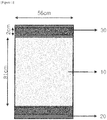
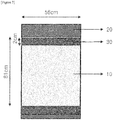
- a Cu layer having a thickness of 2 ⁇ m was formed on a PET film through a vapor deposition method. After an etching resist material is patterned on the film through a photolithography process, a conductive heating pattern area having a metal pattern having a line width of 5 to 8 ⁇ m and a line height of 2 ⁇ m was formed through an etching process. In this case, in the formed conductive heating pattern area, an aperture ratio having a width of 56 cm and a length of 81 cm was 95%, and a surface resistance was 0.50 ohm/square.
- a conductive layer area was formed by forming a non-etching area at upper and lower ends in a longitudinal direction of the heating pattern area. An aperture ratio of the conductive layer area was 0%, and the surface resistance thereof was 0.009 ohm/square.
- a copper foil having a thickness of 50 ⁇ m was attached to the upper and lower conductive layer areas as illustrated in FIG. 1 on the film with a width of 2 cm.
- current of 16.7 A flowed, and the resistance was 0.72 ohm.
- the heat generated in the busbar was slight, and local heat was not generated between the conductive heating pattern area and the conductive layer area.
- Example 2 An experiment was performed by using the same method as Example 1 except that a copper tape with a copper foil of 25 ⁇ m and an adhesive of 25 ⁇ m instead of the copper foil having a thickness of 50 ⁇ m was used on the upper and lower ends. When 12 V was applied to both ends, current of 16.6 A flowed, and the resistance was 0.72 ohm. In this case, as a result of measuring the heating film by a thermo-graphic camera, the heat generated in the busbar was slight, and local heat was not generated between the conductive heating pattern area and the conductive layer area.
- the present invention it is possible to prevent the local heat between the heating element and the busbar from being generated by positioning the busbar on the conductive layer area to control a contact resistance between the heating element and the busbar.
Landscapes
- Engineering & Computer Science (AREA)
- Manufacturing & Machinery (AREA)
- Microelectronics & Electronic Packaging (AREA)
- Surface Heating Bodies (AREA)
Applications Claiming Priority (2)
| Application Number | Priority Date | Filing Date | Title |
|---|---|---|---|
| KR20130018949 | 2013-02-22 | ||
| PCT/KR2014/001432 WO2014129845A1 (ko) | 2013-02-22 | 2014-02-21 | 발열체 및 이의 제조방법 |
Publications (3)
| Publication Number | Publication Date |
|---|---|
| EP2928264A1 EP2928264A1 (en) | 2015-10-07 |
| EP2928264A4 EP2928264A4 (en) | 2016-08-31 |
| EP2928264B1 true EP2928264B1 (en) | 2019-07-24 |
Family
ID=51391560
Family Applications (1)
| Application Number | Title | Priority Date | Filing Date |
|---|---|---|---|
| EP14754485.2A Active EP2928264B1 (en) | 2013-02-22 | 2014-02-21 | Heating element and method for manufacturing same |
Country Status (5)
| Country | Link |
|---|---|
| US (1) | US20150327334A1 (ko) |
| EP (1) | EP2928264B1 (ko) |
| KR (2) | KR20140105408A (ko) |
| CN (1) | CN105247953B (ko) |
| WO (1) | WO2014129845A1 (ko) |
Families Citing this family (18)
| Publication number | Priority date | Publication date | Assignee | Title |
|---|---|---|---|---|
| KR101865441B1 (ko) * | 2014-09-29 | 2018-06-07 | 주식회사 엘지화학 | 발열체 및 이의 제조방법 |
| KR101637920B1 (ko) * | 2015-01-06 | 2016-07-08 | 연세대학교 산학협력단 | 투명필름히터 및 그의 제조방법 |
| JP6178948B1 (ja) | 2015-11-20 | 2017-08-09 | リンテック株式会社 | シート、発熱体、及び発熱装置 |
| KR101858698B1 (ko) | 2016-01-04 | 2018-05-16 | 엘지전자 주식회사 | 차량용 디스플레이 장치 및 차량 |
| CN107172730A (zh) * | 2016-03-07 | 2017-09-15 | 东元奈米应材股份有限公司 | 除冰除霜装置 |
| KR101812024B1 (ko) * | 2016-06-10 | 2017-12-27 | 한국기계연구원 | 열선 및 이를 포함하는 면상 발열 시트 |
| GB201617577D0 (en) | 2016-10-17 | 2016-11-30 | Pilkington Group Limited | Vehicle glazing |
| JP2018085299A (ja) * | 2016-11-25 | 2018-05-31 | 学校法人関東学院 | 面状ヒータ |
| CN106686778B (zh) * | 2017-01-13 | 2023-01-06 | 无锡格菲电子薄膜科技有限公司 | 图案化导电膜提升、控制导电膜阻值的方法及其电发热膜 |
| CN107539280B (zh) * | 2017-02-06 | 2020-08-04 | 福耀集团长春有限公司 | 带有覆盖母线的后风挡玻璃及其有覆盖母线加工工艺 |
| US11291084B2 (en) * | 2017-09-26 | 2022-03-29 | Goodrich Corporation | Method for attaching bus bar to carbon allotrope de-icing sheets |
| KR102058865B1 (ko) * | 2018-04-12 | 2019-12-24 | (주)아이엠 | 초가속 열소재를 이용한 발열 디바이스 및 이의 제조방법 |
| KR102280863B1 (ko) * | 2018-04-20 | 2021-07-23 | 주식회사 엘지화학 | 발열체 및 이의 제조방법 |
| KR102246385B1 (ko) * | 2018-06-19 | 2021-05-03 | (주) 코스텍 | 부스바의 제조장치 및 제조방법 |
| US11477856B2 (en) | 2020-01-21 | 2022-10-18 | Goodrich Corporation | Abraded bus bar area of CNT resistive element |
| JP7476830B2 (ja) * | 2021-03-19 | 2024-05-01 | 豊田合成株式会社 | 近赤外線センサカバーの製造方法 |
| CN113660745B (zh) * | 2021-07-06 | 2022-06-14 | 福耀玻璃工业集团股份有限公司 | 车窗总成 |
| CN113709927B (zh) * | 2021-07-22 | 2023-07-07 | 福耀玻璃工业集团股份有限公司 | 镀膜加热玻璃 |
Family Cites Families (22)
| Publication number | Priority date | Publication date | Assignee | Title |
|---|---|---|---|---|
| US3729616A (en) * | 1971-07-26 | 1973-04-24 | Gen Electric | Electrically heated window |
| US3893234A (en) * | 1972-07-03 | 1975-07-08 | Sierracin Corp | Edge improvement for window with electrically conductive layer |
| US4707586A (en) * | 1981-05-11 | 1987-11-17 | Sierracin Corporation | Electro conductive film system for aircraft windows |
| US4755659A (en) * | 1987-02-03 | 1988-07-05 | Chomerics, Inc. | Combined busbar and electrical lead assembly |
| US4919744A (en) * | 1988-09-30 | 1990-04-24 | Raychem Corporation | Method of making a flexible heater comprising a conductive polymer |
| US5071792A (en) * | 1990-11-05 | 1991-12-10 | Harris Corporation | Process for forming extremely thin integrated circuit dice |
| FR2652037B1 (fr) * | 1989-09-18 | 1992-04-03 | Saint Gobain Vitrage Int | Vitrage feuillete chauffant. |
| DE3937346A1 (de) * | 1989-11-09 | 1991-05-16 | Ver Glaswerke Gmbh | Elektrisch beheizbare autoglasscheibe aus verbundglas |
| DE20316736U1 (de) * | 2003-10-30 | 2004-09-23 | Muchar, Manfred, Dipl.-Kaufm. | Beheizbarer Außenspiegel |
| JP2005302553A (ja) * | 2004-04-13 | 2005-10-27 | U Corporation | 透光性フレキシブルヒータ |
| EP1748034A4 (en) * | 2004-04-28 | 2008-05-28 | Asahi Glass Co Ltd | GLAZING WITH CONDUCTIVE PRINTING AND METHOD OF MANUFACTURE |
| FR2875669B1 (fr) * | 2004-09-17 | 2007-07-06 | Saint Gobain | Structure chauffante electrique |
| DE102004050158B3 (de) * | 2004-10-15 | 2006-04-06 | Saint-Gobain Sekurit Deutschland Gmbh & Co. Kg | Transparente Scheibe mit einer beheizbaren Beschichtung |
| US7627841B2 (en) * | 2006-04-12 | 2009-12-01 | The Regents Of The University Of California, Santa Cruz | Efficient method to predict integrated circuit temperature and power maps |
| GB0612698D0 (en) * | 2006-06-27 | 2006-08-09 | Pilkington Plc | Heatable vehicle glazing |
| DE102007008833A1 (de) * | 2007-02-23 | 2008-08-28 | Saint-Gobain Sekurit Deutschland Gmbh & Co. Kg | Transparente Scheibe mit einer beheizbaren Beschichtung |
| DE102007050286A1 (de) * | 2007-10-18 | 2009-04-23 | Saint-Gobain Sekurit Deutschland Gmbh & Co. Kg | Transparente Scheibe mit einer elektrisch heizbaren Beschichtung |
| EP2257120B1 (en) * | 2008-03-17 | 2013-06-26 | LG Chem, Ltd. | Heating element and manufacturing method for same |
| WO2009116786A2 (ko) * | 2008-03-17 | 2009-09-24 | 주식회사 엘지화학 | 발열체 및 이의 제조방법 |
| CN101978776A (zh) * | 2008-03-17 | 2011-02-16 | Lg化学株式会社 | 加热件及其制备方法 |
| CN101983181B (zh) * | 2008-06-13 | 2015-10-14 | Lg化学株式会社 | 加热件及其制备方法 |
| CN103141157A (zh) * | 2011-01-13 | 2013-06-05 | Lg化学株式会社 | 加热元件及其制造方法 |
-
2014
- 2014-02-21 US US14/655,600 patent/US20150327334A1/en not_active Abandoned
- 2014-02-21 EP EP14754485.2A patent/EP2928264B1/en active Active
- 2014-02-21 WO PCT/KR2014/001432 patent/WO2014129845A1/ko active Application Filing
- 2014-02-21 KR KR1020140020409A patent/KR20140105408A/ko active Application Filing
- 2014-02-21 CN CN201480005910.7A patent/CN105247953B/zh active Active
-
2015
- 2015-08-26 KR KR1020150120161A patent/KR101622887B1/ko active IP Right Grant
Non-Patent Citations (1)
| Title |
|---|
| None * |
Also Published As
| Publication number | Publication date |
|---|---|
| EP2928264A4 (en) | 2016-08-31 |
| CN105247953A (zh) | 2016-01-13 |
| KR20140105408A (ko) | 2014-09-01 |
| KR20150105272A (ko) | 2015-09-16 |
| US20150327334A1 (en) | 2015-11-12 |
| WO2014129845A1 (ko) | 2014-08-28 |
| KR101622887B1 (ko) | 2016-05-19 |
| EP2928264A1 (en) | 2015-10-07 |
| CN105247953B (zh) | 2018-10-19 |
Similar Documents
| Publication | Publication Date | Title |
|---|---|---|
| EP2928264B1 (en) | Heating element and method for manufacturing same | |
| US9029735B2 (en) | Heating element and a production method thereof | |
| EP2284134B1 (en) | Heating element and manufacturing method thereof | |
| KR100940436B1 (ko) | 발열체 및 이의 제조방법 | |
| EP2275389B1 (en) | Heater and manufacturing method for same | |
| KR101865441B1 (ko) | 발열체 및 이의 제조방법 | |
| US9999099B2 (en) | Heating element and a manufacturing method thereof | |
| EP2618632A2 (en) | Heating element and manufacturing method thereof | |
| US20110017719A1 (en) | Heater and manufacturing method for same | |
| CN103180779A (zh) | 包括导电图案的显示设备 | |
| KR101083883B1 (ko) | 부분 발열체 | |
| EP2665337A2 (en) | Heating element and method for manufacturing same | |
| KR102280863B1 (ko) | 발열체 및 이의 제조방법 |
Legal Events
| Date | Code | Title | Description |
|---|---|---|---|
| PUAI | Public reference made under article 153(3) epc to a published international application that has entered the european phase |
Free format text: ORIGINAL CODE: 0009012 |
|
| 17P | Request for examination filed |
Effective date: 20150623 |
|
| AK | Designated contracting states |
Kind code of ref document: A1 Designated state(s): AL AT BE BG CH CY CZ DE DK EE ES FI FR GB GR HR HU IE IS IT LI LT LU LV MC MK MT NL NO PL PT RO RS SE SI SK SM TR |
|
| AX | Request for extension of the european patent |
Extension state: BA ME |
|
| DAX | Request for extension of the european patent (deleted) | ||
| RA4 | Supplementary search report drawn up and despatched (corrected) |
Effective date: 20160801 |
|
| RIC1 | Information provided on ipc code assigned before grant |
Ipc: H01C 17/00 20060101ALI20160726BHEP Ipc: H05B 3/28 20060101ALI20160726BHEP Ipc: H05B 1/02 20060101ALI20160726BHEP Ipc: H05B 3/84 20060101AFI20160726BHEP Ipc: H01C 17/28 20060101ALI20160726BHEP Ipc: H05B 3/86 20060101ALI20160726BHEP |
|
| STAA | Information on the status of an ep patent application or granted ep patent |
Free format text: STATUS: EXAMINATION IS IN PROGRESS |
|
| 17Q | First examination report despatched |
Effective date: 20170810 |
|
| GRAP | Despatch of communication of intention to grant a patent |
Free format text: ORIGINAL CODE: EPIDOSNIGR1 |
|
| STAA | Information on the status of an ep patent application or granted ep patent |
Free format text: STATUS: GRANT OF PATENT IS INTENDED |
|
| INTG | Intention to grant announced |
Effective date: 20190215 |
|
| GRAS | Grant fee paid |
Free format text: ORIGINAL CODE: EPIDOSNIGR3 |
|
| GRAA | (expected) grant |
Free format text: ORIGINAL CODE: 0009210 |
|
| STAA | Information on the status of an ep patent application or granted ep patent |
Free format text: STATUS: THE PATENT HAS BEEN GRANTED |
|
| AK | Designated contracting states |
Kind code of ref document: B1 Designated state(s): AL AT BE BG CH CY CZ DE DK EE ES FI FR GB GR HR HU IE IS IT LI LT LU LV MC MK MT NL NO PL PT RO RS SE SI SK SM TR |
|
| REG | Reference to a national code |
Ref country code: GB Ref legal event code: FG4D |
|
| REG | Reference to a national code |
Ref country code: CH Ref legal event code: EP |
|
| REG | Reference to a national code |
Ref country code: DE Ref legal event code: R096 Ref document number: 602014050495 Country of ref document: DE |
|
| REG | Reference to a national code |
Ref country code: AT Ref legal event code: REF Ref document number: 1159873 Country of ref document: AT Kind code of ref document: T Effective date: 20190815 |
|
| REG | Reference to a national code |
Ref country code: IE Ref legal event code: FG4D |
|
| REG | Reference to a national code |
Ref country code: SE Ref legal event code: TRGR |
|
| REG | Reference to a national code |
Ref country code: NL Ref legal event code: MP Effective date: 20190724 |
|
| REG | Reference to a national code |
Ref country code: LT Ref legal event code: MG4D |
|
| REG | Reference to a national code |
Ref country code: AT Ref legal event code: MK05 Ref document number: 1159873 Country of ref document: AT Kind code of ref document: T Effective date: 20190724 |
|
| PG25 | Lapsed in a contracting state [announced via postgrant information from national office to epo] |
Ref country code: LT Free format text: LAPSE BECAUSE OF FAILURE TO SUBMIT A TRANSLATION OF THE DESCRIPTION OR TO PAY THE FEE WITHIN THE PRESCRIBED TIME-LIMIT Effective date: 20190724 Ref country code: HR Free format text: LAPSE BECAUSE OF FAILURE TO SUBMIT A TRANSLATION OF THE DESCRIPTION OR TO PAY THE FEE WITHIN THE PRESCRIBED TIME-LIMIT Effective date: 20190724 Ref country code: FI Free format text: LAPSE BECAUSE OF FAILURE TO SUBMIT A TRANSLATION OF THE DESCRIPTION OR TO PAY THE FEE WITHIN THE PRESCRIBED TIME-LIMIT Effective date: 20190724 Ref country code: NO Free format text: LAPSE BECAUSE OF FAILURE TO SUBMIT A TRANSLATION OF THE DESCRIPTION OR TO PAY THE FEE WITHIN THE PRESCRIBED TIME-LIMIT Effective date: 20191024 Ref country code: BG Free format text: LAPSE BECAUSE OF FAILURE TO SUBMIT A TRANSLATION OF THE DESCRIPTION OR TO PAY THE FEE WITHIN THE PRESCRIBED TIME-LIMIT Effective date: 20191024 Ref country code: AT Free format text: LAPSE BECAUSE OF FAILURE TO SUBMIT A TRANSLATION OF THE DESCRIPTION OR TO PAY THE FEE WITHIN THE PRESCRIBED TIME-LIMIT Effective date: 20190724 Ref country code: PT Free format text: LAPSE BECAUSE OF FAILURE TO SUBMIT A TRANSLATION OF THE DESCRIPTION OR TO PAY THE FEE WITHIN THE PRESCRIBED TIME-LIMIT Effective date: 20191125 Ref country code: NL Free format text: LAPSE BECAUSE OF FAILURE TO SUBMIT A TRANSLATION OF THE DESCRIPTION OR TO PAY THE FEE WITHIN THE PRESCRIBED TIME-LIMIT Effective date: 20190724 |
|
| PG25 | Lapsed in a contracting state [announced via postgrant information from national office to epo] |
Ref country code: RS Free format text: LAPSE BECAUSE OF FAILURE TO SUBMIT A TRANSLATION OF THE DESCRIPTION OR TO PAY THE FEE WITHIN THE PRESCRIBED TIME-LIMIT Effective date: 20190724 Ref country code: LV Free format text: LAPSE BECAUSE OF FAILURE TO SUBMIT A TRANSLATION OF THE DESCRIPTION OR TO PAY THE FEE WITHIN THE PRESCRIBED TIME-LIMIT Effective date: 20190724 Ref country code: AL Free format text: LAPSE BECAUSE OF FAILURE TO SUBMIT A TRANSLATION OF THE DESCRIPTION OR TO PAY THE FEE WITHIN THE PRESCRIBED TIME-LIMIT Effective date: 20190724 Ref country code: ES Free format text: LAPSE BECAUSE OF FAILURE TO SUBMIT A TRANSLATION OF THE DESCRIPTION OR TO PAY THE FEE WITHIN THE PRESCRIBED TIME-LIMIT Effective date: 20190724 Ref country code: GR Free format text: LAPSE BECAUSE OF FAILURE TO SUBMIT A TRANSLATION OF THE DESCRIPTION OR TO PAY THE FEE WITHIN THE PRESCRIBED TIME-LIMIT Effective date: 20191025 Ref country code: IS Free format text: LAPSE BECAUSE OF FAILURE TO SUBMIT A TRANSLATION OF THE DESCRIPTION OR TO PAY THE FEE WITHIN THE PRESCRIBED TIME-LIMIT Effective date: 20191124 |
|
| PG25 | Lapsed in a contracting state [announced via postgrant information from national office to epo] |
Ref country code: TR Free format text: LAPSE BECAUSE OF FAILURE TO SUBMIT A TRANSLATION OF THE DESCRIPTION OR TO PAY THE FEE WITHIN THE PRESCRIBED TIME-LIMIT Effective date: 20190724 |
|
| PG25 | Lapsed in a contracting state [announced via postgrant information from national office to epo] |
Ref country code: EE Free format text: LAPSE BECAUSE OF FAILURE TO SUBMIT A TRANSLATION OF THE DESCRIPTION OR TO PAY THE FEE WITHIN THE PRESCRIBED TIME-LIMIT Effective date: 20190724 Ref country code: PL Free format text: LAPSE BECAUSE OF FAILURE TO SUBMIT A TRANSLATION OF THE DESCRIPTION OR TO PAY THE FEE WITHIN THE PRESCRIBED TIME-LIMIT Effective date: 20190724 Ref country code: RO Free format text: LAPSE BECAUSE OF FAILURE TO SUBMIT A TRANSLATION OF THE DESCRIPTION OR TO PAY THE FEE WITHIN THE PRESCRIBED TIME-LIMIT Effective date: 20190724 Ref country code: IT Free format text: LAPSE BECAUSE OF FAILURE TO SUBMIT A TRANSLATION OF THE DESCRIPTION OR TO PAY THE FEE WITHIN THE PRESCRIBED TIME-LIMIT Effective date: 20190724 Ref country code: DK Free format text: LAPSE BECAUSE OF FAILURE TO SUBMIT A TRANSLATION OF THE DESCRIPTION OR TO PAY THE FEE WITHIN THE PRESCRIBED TIME-LIMIT Effective date: 20190724 |
|
| PG25 | Lapsed in a contracting state [announced via postgrant information from national office to epo] |
Ref country code: SM Free format text: LAPSE BECAUSE OF FAILURE TO SUBMIT A TRANSLATION OF THE DESCRIPTION OR TO PAY THE FEE WITHIN THE PRESCRIBED TIME-LIMIT Effective date: 20190724 Ref country code: IS Free format text: LAPSE BECAUSE OF FAILURE TO SUBMIT A TRANSLATION OF THE DESCRIPTION OR TO PAY THE FEE WITHIN THE PRESCRIBED TIME-LIMIT Effective date: 20200224 Ref country code: CZ Free format text: LAPSE BECAUSE OF FAILURE TO SUBMIT A TRANSLATION OF THE DESCRIPTION OR TO PAY THE FEE WITHIN THE PRESCRIBED TIME-LIMIT Effective date: 20190724 Ref country code: SK Free format text: LAPSE BECAUSE OF FAILURE TO SUBMIT A TRANSLATION OF THE DESCRIPTION OR TO PAY THE FEE WITHIN THE PRESCRIBED TIME-LIMIT Effective date: 20190724 |
|
| REG | Reference to a national code |
Ref country code: DE Ref legal event code: R097 Ref document number: 602014050495 Country of ref document: DE |
|
| PLBE | No opposition filed within time limit |
Free format text: ORIGINAL CODE: 0009261 |
|
| STAA | Information on the status of an ep patent application or granted ep patent |
Free format text: STATUS: NO OPPOSITION FILED WITHIN TIME LIMIT |
|
| PG2D | Information on lapse in contracting state deleted |
Ref country code: IS |
|
| 26N | No opposition filed |
Effective date: 20200603 |
|
| PG25 | Lapsed in a contracting state [announced via postgrant information from national office to epo] |
Ref country code: SI Free format text: LAPSE BECAUSE OF FAILURE TO SUBMIT A TRANSLATION OF THE DESCRIPTION OR TO PAY THE FEE WITHIN THE PRESCRIBED TIME-LIMIT Effective date: 20190724 |
|
| REG | Reference to a national code |
Ref country code: CH Ref legal event code: PL |
|
| REG | Reference to a national code |
Ref country code: BE Ref legal event code: MM Effective date: 20200229 |
|
| PG25 | Lapsed in a contracting state [announced via postgrant information from national office to epo] |
Ref country code: LU Free format text: LAPSE BECAUSE OF NON-PAYMENT OF DUE FEES Effective date: 20200221 Ref country code: MC Free format text: LAPSE BECAUSE OF FAILURE TO SUBMIT A TRANSLATION OF THE DESCRIPTION OR TO PAY THE FEE WITHIN THE PRESCRIBED TIME-LIMIT Effective date: 20190724 |
|
| PG25 | Lapsed in a contracting state [announced via postgrant information from national office to epo] |
Ref country code: CH Free format text: LAPSE BECAUSE OF NON-PAYMENT OF DUE FEES Effective date: 20200229 Ref country code: LI Free format text: LAPSE BECAUSE OF NON-PAYMENT OF DUE FEES Effective date: 20200229 |
|
| PG25 | Lapsed in a contracting state [announced via postgrant information from national office to epo] |
Ref country code: IE Free format text: LAPSE BECAUSE OF NON-PAYMENT OF DUE FEES Effective date: 20200221 |
|
| PG25 | Lapsed in a contracting state [announced via postgrant information from national office to epo] |
Ref country code: BE Free format text: LAPSE BECAUSE OF NON-PAYMENT OF DUE FEES Effective date: 20200229 |
|
| PG25 | Lapsed in a contracting state [announced via postgrant information from national office to epo] |
Ref country code: MT Free format text: LAPSE BECAUSE OF FAILURE TO SUBMIT A TRANSLATION OF THE DESCRIPTION OR TO PAY THE FEE WITHIN THE PRESCRIBED TIME-LIMIT Effective date: 20190724 Ref country code: CY Free format text: LAPSE BECAUSE OF FAILURE TO SUBMIT A TRANSLATION OF THE DESCRIPTION OR TO PAY THE FEE WITHIN THE PRESCRIBED TIME-LIMIT Effective date: 20190724 |
|
| PG25 | Lapsed in a contracting state [announced via postgrant information from national office to epo] |
Ref country code: MK Free format text: LAPSE BECAUSE OF FAILURE TO SUBMIT A TRANSLATION OF THE DESCRIPTION OR TO PAY THE FEE WITHIN THE PRESCRIBED TIME-LIMIT Effective date: 20190724 |
|
| PGFP | Annual fee paid to national office [announced via postgrant information from national office to epo] |
Ref country code: DE Payment date: 20240122 Year of fee payment: 11 Ref country code: GB Payment date: 20240122 Year of fee payment: 11 |
|
| PGFP | Annual fee paid to national office [announced via postgrant information from national office to epo] |
Ref country code: SE Payment date: 20240123 Year of fee payment: 11 Ref country code: FR Payment date: 20240123 Year of fee payment: 11 |