EP2926357B1 - Tripping device for circuit breaker - Google Patents
Tripping device for circuit breaker Download PDFInfo
- Publication number
- EP2926357B1 EP2926357B1 EP13799284.8A EP13799284A EP2926357B1 EP 2926357 B1 EP2926357 B1 EP 2926357B1 EP 13799284 A EP13799284 A EP 13799284A EP 2926357 B1 EP2926357 B1 EP 2926357B1
- Authority
- EP
- European Patent Office
- Prior art keywords
- bimetal
- current path
- trigger device
- mounting device
- circuit breaker
- Prior art date
- Legal status (The legal status is an assumption and is not a legal conclusion. Google has not performed a legal analysis and makes no representation as to the accuracy of the status listed.)
- Active
Links
Images

Classifications
-
- H—ELECTRICITY
- H01—ELECTRIC ELEMENTS
- H01H—ELECTRIC SWITCHES; RELAYS; SELECTORS; EMERGENCY PROTECTIVE DEVICES
- H01H37/00—Thermally-actuated switches
- H01H37/02—Details
- H01H37/32—Thermally-sensitive members
- H01H37/52—Thermally-sensitive members actuated due to deflection of bimetallic element
-
- H—ELECTRICITY
- H01—ELECTRIC ELEMENTS
- H01H—ELECTRIC SWITCHES; RELAYS; SELECTORS; EMERGENCY PROTECTIVE DEVICES
- H01H71/00—Details of the protective switches or relays covered by groups H01H73/00 - H01H83/00
- H01H71/10—Operating or release mechanisms
- H01H71/12—Automatic release mechanisms with or without manual release
- H01H71/14—Electrothermal mechanisms
- H01H71/16—Electrothermal mechanisms with bimetal element
-
- H—ELECTRICITY
- H01—ELECTRIC ELEMENTS
- H01H—ELECTRIC SWITCHES; RELAYS; SELECTORS; EMERGENCY PROTECTIVE DEVICES
- H01H37/00—Thermally-actuated switches
- H01H37/02—Details
- H01H37/04—Bases; Housings; Mountings
-
- H—ELECTRICITY
- H01—ELECTRIC ELEMENTS
- H01H—ELECTRIC SWITCHES; RELAYS; SELECTORS; EMERGENCY PROTECTIVE DEVICES
- H01H71/00—Details of the protective switches or relays covered by groups H01H73/00 - H01H83/00
- H01H71/10—Operating or release mechanisms
- H01H71/12—Automatic release mechanisms with or without manual release
- H01H71/14—Electrothermal mechanisms
- H01H71/16—Electrothermal mechanisms with bimetal element
- H01H71/164—Heating elements
- H01H2071/165—Heating elements the bimetal being inductively heated, e.g. load current does not pass through bimetal
Definitions
- the invention relates to a tripping device for circuit breakers.
- circuit breakers use electronic overload tripping devices or triggers.
- Thermal or thermomagnetic actuators which use a bimetallic strip or a bimetallic strip, have hitherto not been suitable for use at such high rated currents for various reasons.
- the tripping time for thermal triggers is determined by the temperature at the bimetal and the temperature-dependent deflection of the bimetal.
- the bimetal is thereby connected to the conductor at one or more points.
- the heating of the bimetal therefore occurs mainly at this connection point (s).
- the bimetal takes a relatively long period of time to reach the deflection required to initiate the process.
- the normally required tripping times are therefore not achievable at high currents with bimetal triggers.
- the self-protection of the circuit breaker is not guaranteed by the too long tripping times, especially at a multiple of the rated current, since too high I 2 t values can occur.
- bimetal actuators Another disadvantage of bimetal actuators is that the triggering accuracy at high currents can be influenced by external influences such as by a draft or the installation position of a circuit breaker, since the bimetal is usually mounted freestanding in circuit breakers. This can cause circuit breakers with bimetallic actuators to trip due to environmental influences at different currents. When measuring the tripping time, in particular at a multiple of the rated current, this is noticeable by different tripping times.
- a relay that has a U-shaped bimetal disposed approximately parallel to a U-shaped portion of a current path of the relay.
- the US patent US 3, 296 398 A discloses a circuit breaker with a thermal overcurrent protection, in which a bimetallic actuator is disposed approximately parallel to a resistance heater and together with this in a housing of the circuit breaker.
- the US patent application US2006 / 0232905 A1 also describes a thermal overcurrent protection device in which a bimetallic switch is either embedded in an electrical current-carrying conductor section with increased electrical resistance or is cast together with heating wires through which electrical heating current flows.
- the US patent US 3 422 317 A relates to a thermal overcurrent protection device with bimetals, which are designed U-shaped and arranged approximately parallel to current paths. To compensate for environmental influences, a separate U-shaped designed bimetal is provided which is exposed to the ambient temperature. An arm of this separate bimetal is coupled to arms of the bumps associated with the current paths via a lever to compensate for the influence of the ambient temperature on the triggering mechanism of the bumps associated with the current paths via the lever action.
- Object of the present invention is therefore to propose an improved tripping device for a circuit breaker, which indeed uses a bimetal, but in which the initially described disadvantage of excessive dependence on environmental or environmental influences is reduced.
- An object of the present invention is to provide a bearing device for the approximately parallel to a current path of a circuit breaker to be arranged bimetal of a trigger, which is designed such that of the Radial radiated heat can heat the bimetal almost over its entire length and can shield the bimetal from environmental influences.
- the deflection of the bimetal is achieved by the radiated heat from the current path and, if appropriate, in addition to the heating of an attachment point of the bimetal on the current path.
- the bimetal is located mainly within the heat radiation, so that external influences on the heating and deflection of the bimetal are reduced. Above all, the influence of the ambient temperature and the influence of air currents can be reduced by the storage facility.
- An embodiment of the invention now relates to a tripping device for circuit breakers with a bimetallic device intended to be arranged in the vicinity of a circuit of a circuit breaker for controlling tripping of the circuit breaker and a bimetal bearing device in which the bimetal is inserted and which is designed such that it Bit metal in an arrangement approximately parallel to a current path of the circuit breaker so encloses that radiated from the current path heat can heat the bimetal almost over its entire length and the bimetal is shielded from environmental influences.
- the current path can also be formed by shunts in the sense of the present invention.
- the bimetallic bearing device may have a bottom on which the bimetal is fixed at a foot point and which is bounded by two side walls which extend approximately parallel to the bimetal and are designed such that the bimetal is shielded from environmental influences.
- a kind of pocket for the bimetal is formed, in which the radiated heat from the current path is transferred to the bimetal and thus can cause a faster heating of the bimetal, as a result, the tripping of the circuit breaker can be accelerated.
- the bimetal can be fixed to the ground in such a way that its active side lies opposite the current path. As a result, the heating and thus the deflection of the bimetal can be further accelerated by the radiated heat from the current path and ultimately the triggering.
- the sidewalls may also be configured to extend at least partially beyond the bimetal.
- the pocket-like receptacle for the bimetal formed by the bottom and the side walls can more efficiently concentrate the heat radiated from the flow path onto the bimetal, thus ensuring the fastest possible and defined heating of the bimetal and even better shielding from environmental influences.
- the bimetallic bearing device may be designed to completely enclose the bimetal, in particular it may be formed both as a pocket, sleeve or tube into which the bimetal is inserted. This results in a very constant and rapid heat radiation to the bimetal. Complete enclosing does not mean a hermetic decoupling of the bimetal from the environment. Rather, there are still openings for example, a movable bimetallic pin or pin of the triggering device and for inserting the bimetal in the pocket, sleeve or tube available.
- the bimetallic bearing device may also be formed by the current path itself.
- the bimetal is coupled to the current path at least at an attachment point, so that the heat transfer from the current path to the bimetal is particularly efficient. This has the advantage that the bimetal heats up faster and thus the desired deflection earlier, in particular by about 30% earlier than in the comparison described above conventional use of the bimetal without bearing device can be achieved.
- the bimetallic bearing device may have an L, U, O or circular, spline shape. Such forms may have manufacturing advantages and also favor the concentration of heat around the bimetal.
- a further embodiment relates to a circuit breaker, in particular for high rated currents, with at least one current path and a tripping device according to the invention and as described herein per current path, wherein the tripping device associated with a current path is arranged with respect to the current path, that the bimetal of the tripping device in a predetermined distance is approximately parallel to the current path and can be heated by the heat radiated from the current path.
- the bimetallic bearing device is formed as a separate element to which the bimetal is fixed and which is mounted on the current path.
- the bimetal is effectively shielded from environmental influences such as air currents, so that the heat given off by the current path can act almost unhindered on the bimetal.
- the required tripping time of the circuit breaker tripping device can be better maintained because environmental or environmental influences through the shield of the bimetal have less influence on the heating of the bimetal and thus the triggering.
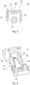
- triggering device 10 has a bimetal 14 in the form of a strip which is arranged approximately parallel to a current path 12 of the circuit breaker.
- the distance between the flow path 12 and bimetal 14 is In this case, such that the heat developed when the rated current of the current path 12 is exceeded and radiated from the current path 12 produces a deflection of the bimetal within a predetermined period of time, so that tripping in the circuit breaker can take place within a defined period of time.
- the bimetal 14 is fixed at a base 20 to a bottom 18 of a bearing device 16 for the bimetal 14.
- the bearing device 16 is formed as a separate component. But it can be like the one in Fig. 3 embodiment shown also be formed by the current path itself.
- the bearing device 16 also has two side walls 22, which together with the bottom 18 form a kind of pocket for the bimetal 14.
- the side walls 22 extend over the bimetal 14, as in Fig. 2 is recognizable. You can also at least partially via the current path 12 (dashed extensions of the side walls 22 in Fig. 2 ), so that the current path 12 and the bimetal 14 can be almost completely covered by the bearing device.
- the side walls 22 may extend the length of the bent bimetal 14.
- the storage facility completely, ie to make closed from all sides, so that the current path 12 and the bimetal 14 are housed in a common housing.
- the bearing means 16 comprise a pocket, a tube or a sleeve, which enclose the flow path 12 and the bimetal 14.
- the storage device 16 fulfills two tasks: on the one hand, it effects a distribution of the heat radiated from the current path 12 over almost the entire length of the bimetal 14, since the radiated heat develops within the created by the bottom 18 and the side walls 22 of the storage device 16 space and so relatively evenly heat the bimetal 14 located in the room.
- the bearing device 16 forms a kind of shielding of the bimetal 14 from environmental influences such as air currents or the ambient temperature.
- the bimetallic bearing means 16 has a U-shaped cross-section. However, it may also have other cross-sectional shapes, such as an L, O or circular, spline shape.
- the shape of the bearing device can be chosen depending on the application and adapted to the conditions of use.
- FIG. 1 and 2 shown embodiment may be to use the storage device 16 itself as a current path.
- the flow path 12 in this case may be a shunt which may serve to reduce mass at the bearing means.
- the bimetallic bearing device is formed by the current path itself, i. not formed as a separate element.
- the bimetal is in this case fixed directly to at least one point on the current path, whereby a relatively rapid heating of the bimetal and thus short tripping time of the triggering device can be achieved.
- Fig. 3 shows a further embodiment of the tripping device 11 according to the invention, in which the bimetallic bearing device 17 is formed by the current path 13 of a circuit breaker and therefore the current path 13 forms part of the tripping device.
- the bimetallic bearing device 17 is an integral part of the current path 13.
- the current path 13 is for this purpose formed such that it forms a kind of pocket for the bimetal 15, which is fixed directly via a foot 21 to the current path 13 at a bottom 19 of the bearing device 17, which is formed by a specially trained portion of the current path 13 ,
- the bimetal 15 is arranged approximately parallel to the flow path 13 suspended above this. It is heated on the one hand on the foot 21, and on the other hand almost over its entire length by the radiated from the current path 13 heat.
- the tripping device 11 shown with the current path 13 may be formed for example as part of a current path of a circuit breaker, whereby it can be installed with relatively little installation effort in the circuit breaker.
- the shown triggering device 11 already be preassembled, whereby they must be installed for mounting only in the circuit breaker.
- the present invention is particularly suitable for use in circuit breakers with thermal triggers and can cause a reduction in the tripping times and the environmental or environmental influences, especially in thermomagnetic circuit breakers for rated currents of 250 amps or greater. Furthermore, the invention provides a cost-effective alternative to the standard electronic overload releases for circuit breakers for nominal currents of 630 amps or greater.
Description
Die Erfindung betrifft eine Auslösevorrichtung für Leistungsschalter.The invention relates to a tripping device for circuit breakers.
Üblicherweise werden bei hohen Nennströmen von 630 Ampere oder höher bei Leistungsschaltern elektronische Überlast-Auslösevorrichtungen bzw. -Auslöser eingesetzt. Thermische oder thermomagnetische Auslöser, die ein Bimetall bzw. einen Bimetallstreifen einsetzen, eigneten sich bisher aus verschiedenen Gründen nicht für den Einsatz bei solch hohen Nennströmen.Usually at high rated currents of 630 amperes or higher, circuit breakers use electronic overload tripping devices or triggers. Thermal or thermomagnetic actuators, which use a bimetallic strip or a bimetallic strip, have hitherto not been suitable for use at such high rated currents for various reasons.
Während bei elektronischen Auslösern der Strom elektronisch gemessen und die gewünschte Auslösezeit eingestellt werden kann, wird die Auslösezeit bei thermischen Auslösern durch die Temperatur am Bimetall und die temperaturabhängige Ausbiegung des Bimetalls bestimmt. Das Bimetall wird dabei an einem oder mehreren Punkt(en) mit dem Stromleiter verbunden. Die Erwärmung des Bimetalls erfolgt daher hauptsächlich an diesem(n) Verbindungspunkt(en). Das führt dazu, dass das Bimetall eine verhältnismäßig lange Zeitdauer benötigt, um die zum Auslösen in der Regel geforderte Ausbiegung zu erreichen. Die üblicherweise geforderten Auslösezeiten sind daher bei hohen Strömen mit Bimetall-Auslösern nicht erreichbar. Auch der Selbstschutz des Leistungsschalters ist durch die zu langen Auslösezeiten vor allem bei einem Vielfachen des Nennstroms nicht gewährleistet, da zu hohe I2t-Werte auftreten können.While in electronic triggers the current can be measured electronically and the desired tripping time can be set, the tripping time for thermal triggers is determined by the temperature at the bimetal and the temperature-dependent deflection of the bimetal. The bimetal is thereby connected to the conductor at one or more points. The heating of the bimetal therefore occurs mainly at this connection point (s). As a result, the bimetal takes a relatively long period of time to reach the deflection required to initiate the process. The normally required tripping times are therefore not achievable at high currents with bimetal triggers. The self-protection of the circuit breaker is not guaranteed by the too long tripping times, especially at a multiple of the rated current, since too high I 2 t values can occur.
Ein weiterer Nachteil von Bimetall-Auslösern besteht darin, dass die Auslösegenauigkeit bei hohen Strömen durch äußere Einflüsse wie beispielsweise durch einen Luftzug oder die Einbaulage eines Leistungsschalters beeinflusst werden kann, da das Bimetall bei Leistungsschaltern üblicherweise freistehend angebracht wird. Das kann dazu führen, dass Leistungsschalter mit Bimetall-Auslösern aufgrund von Umwelteinflüssen bei unterschiedlichen Strömen auslösen. Bei der Messung der Auslösezeit, insbesondere bei einem Vielfachen des Nennstroms, macht sich dies durch unterschiedliche Auslösezeiten bemerkbar.Another disadvantage of bimetal actuators is that the triggering accuracy at high currents can be influenced by external influences such as by a draft or the installation position of a circuit breaker, since the bimetal is usually mounted freestanding in circuit breakers. This can cause circuit breakers with bimetallic actuators to trip due to environmental influences at different currents. When measuring the tripping time, in particular at a multiple of the rated current, this is noticeable by different tripping times.
Aus der US-Patentschrift
Die US-Patentschrift
Die US-Patentanmeldung
Die US-Patentschrift
Aufgabe der vorliegenden Erfindung ist es daher, eine verbesserte Auslösevorrichtung für einen Leistungsschalter vorzuschlagen, die zwar ein Bimetall einsetzt, bei der aber der eingangs geschilderte Nachteil einer zu großen Abhängigkeit von Umgebungs- bzw. Umwelteinflüssen verringert ist.Object of the present invention is therefore to propose an improved tripping device for a circuit breaker, which indeed uses a bimetal, but in which the initially described disadvantage of excessive dependence on environmental or environmental influences is reduced.
Diese Aufgabe wird durch die Gegenstände der unabhängigen Ansprüche gelöst. Weitere Ausgestaltungen der Erfindung sind Gegenstand der abhängigen Ansprüche.This object is solved by the subject matters of the independent claims. Further embodiments of the invention are the subject of the dependent claims.
Ein der vorliegenden Erfindung zugrunde liegender Gedanke besteht darin, eine Lagereinrichtung für das etwa parallel zu einer Strombahn eines Leistungsschalter anzuordnende Bimetall eines Auslösers vorzusehen, die derart ausgebildet ist, dass von der Strombahn abgestrahlte Wärme das Bimetall nahezu über dessen gesamte Länge erwärmen kann und das Bimetall vor Umgebungseinflüssen abschirmen kann. Die Ausbiegung des Bimetalls wird durch die von der Strombahn abgestrahlte Wärme und ggf. zusätzlich der Erwärmung eines Befestigungspunktes des Bimetalls an der Strombahn erreicht. Durch die Abschirmung vor Umgebungseinflüssen durch die Bimetall-Lagereinrichtung befindet sich das Bimetall hauptsächlich innerhalb der Wärmestrahlung, so dass äußere Einflüsse auf die Erwärmung und Ausbiegung des Bimetalls reduziert werden. Vor allem der Einfluss der Umgebungstemperatur sowie die Beeinflussung durch Luftströme können durch die Lagereinrichtung verringert werden.An object of the present invention is to provide a bearing device for the approximately parallel to a current path of a circuit breaker to be arranged bimetal of a trigger, which is designed such that of the Radial radiated heat can heat the bimetal almost over its entire length and can shield the bimetal from environmental influences. The deflection of the bimetal is achieved by the radiated heat from the current path and, if appropriate, in addition to the heating of an attachment point of the bimetal on the current path. By shielding against environmental influences by the bimetallic bearing device, the bimetal is located mainly within the heat radiation, so that external influences on the heating and deflection of the bimetal are reduced. Above all, the influence of the ambient temperature and the influence of air currents can be reduced by the storage facility.
Eine Ausführungsform der Erfindung betrifft nun eine Auslösevorrichtung für Leistungsschalter mit einem zur Anordnung in der Nähe einer Strombahn eines Leistungsschalters vorgesehenen Bimetall zum Steuern einer Auslösung des Leistungsschalters und einer Bimetall-Lagereinrichtung, in die das Bimetall eingesetzt ist und die derart ausgebildet ist, dass sie das Bitmetall bei einer Anordnung etwa parallel zu einer Strombahn des Leistungsschalters so umschließt, dass von der Strombahn abgestrahlte Wärme das Bimetall nahezu über dessen gesamte Länge erwärmen kann und das Bimetall vor Umgebungseinflüssen abgeschirmt wird. Die Strombahn kann im Sinne der vorliegenden Erfindung auch durch Shunts gebildet sein.An embodiment of the invention now relates to a tripping device for circuit breakers with a bimetallic device intended to be arranged in the vicinity of a circuit of a circuit breaker for controlling tripping of the circuit breaker and a bimetal bearing device in which the bimetal is inserted and which is designed such that it Bit metal in an arrangement approximately parallel to a current path of the circuit breaker so encloses that radiated from the current path heat can heat the bimetal almost over its entire length and the bimetal is shielded from environmental influences. The current path can also be formed by shunts in the sense of the present invention.
Die Bimetall-Lagereinrichtung kann einen Boden aufweisen, an dem das Bimetall an einem Fußpunkt fixiert ist und der von zwei Seitenwänden begrenzt ist, die sich etwa parallel zum Bimetall erstrecken und derart gestaltet sind, dass das Bimetall vor Umgebungseinflüssen abgeschirmt ist. Hierdurch wird eine Art Tasche für das Bimetall gebildet, in der sich die von der Strombahn abgestrahlte Wärme auf das Bimetall überträgt und somit eine schnellere Erwärmung des Bimetalls bewirken kann, wodurch als Ergebnis die Auslösung des Leistungsschalters beschleunigt werden kann.The bimetallic bearing device may have a bottom on which the bimetal is fixed at a foot point and which is bounded by two side walls which extend approximately parallel to the bimetal and are designed such that the bimetal is shielded from environmental influences. As a result, a kind of pocket for the bimetal is formed, in which the radiated heat from the current path is transferred to the bimetal and thus can cause a faster heating of the bimetal, as a result, the tripping of the circuit breaker can be accelerated.
Das Bimetall kann derart am Boden fixiert sein, dass seine aktive Seite gegenüber der Strombahn liegt. Hierdurch kann die Erwärmung und damit die Ausbiegung des Bimetalls durch die von der Strombahn abgestrahlte Wärme und letztlich die Auslösung nochmals beschleunigt werden.The bimetal can be fixed to the ground in such a way that its active side lies opposite the current path. As a result, the heating and thus the deflection of the bimetal can be further accelerated by the radiated heat from the current path and ultimately the triggering.
Die Seitenwände können ferner derart gestaltet sein, dass sie sich zumindest teilweise über das Bimetall hinaus erstrecken. Dadurch kann der durch den Boden und die Seitenwände gebildete Taschen-artige Aufnahme für das Bimetall noch effizienter die von der Strombahn abgestrahlte Wärme auf das Bimetall konzentrieren, so dass eine möglichst schnelle und definierte Erwärmung des Bimetalls und eine noch bessere Abschirmung vor Umgebungseinflüssen gewährleistet ist.The sidewalls may also be configured to extend at least partially beyond the bimetal. As a result, the pocket-like receptacle for the bimetal formed by the bottom and the side walls can more efficiently concentrate the heat radiated from the flow path onto the bimetal, thus ensuring the fastest possible and defined heating of the bimetal and even better shielding from environmental influences.
Die Bimetall-Lagereinrichtung kann derart ausgebildet sein, das Bimetall vollständig zu umschließen, insbesondere kann sie sowohl als Tasche, Hülse oder Rohr ausgebildet sein , in welche das Bimetall eingeführt ist. Hierdurch erfolgt eine sehr konstante und schnelle Wärmeabstrahlung auf das Bimetall. Vollständiges Umschließen bedeutet hierbei nicht eine hermetische Abkopplung des Bimetalls von der Umgebung. Vielmehr sind immer noch Öffnungen für beispielsweise einen vom Bimetall bewegbaren Zapfen oder Stift der Auslösevorrichtung und zum Einführen des Bimetalls in die Tasche, Hülse oder das Rohr vorhanden.The bimetallic bearing device may be designed to completely enclose the bimetal, in particular it may be formed both as a pocket, sleeve or tube into which the bimetal is inserted. This results in a very constant and rapid heat radiation to the bimetal. Complete enclosing does not mean a hermetic decoupling of the bimetal from the environment. Rather, there are still openings for example, a movable bimetallic pin or pin of the triggering device and for inserting the bimetal in the pocket, sleeve or tube available.
Die Bimetall-Lagereinrichtung kann auch durch die Strombahn selbst gebildet sein. In diesem Fall ist das Bimetall zumindest an einem Befestigungspunkt mit der Strombahn gekoppelt, so dass die Wärmeübertragung von der Strombahn auf das Bimetall besonders effizient ist. Dies hat den Vorteil, dass das Bimetall schneller erwärmt und dadurch die gewünschte Ausbiegung früher, insbesondere um etwa 30 % früher als im Vergleich eingangs beschriebenen herkömmlichen Einsatz des Bimetalls ohne Lagereinrichtung erreicht werden kann.The bimetallic bearing device may also be formed by the current path itself. In this case, the bimetal is coupled to the current path at least at an attachment point, so that the heat transfer from the current path to the bimetal is particularly efficient. This has the advantage that the bimetal heats up faster and thus the desired deflection earlier, in particular by about 30% earlier than in the comparison described above conventional use of the bimetal without bearing device can be achieved.
Schließlich kann die Bimetall-Lagereinrichtung eine L-, U-, O- oder Kreis-, Spline-Form aufweisen. Derartige Formen können fertigungstechnische Vorteile besitzen und zudem die Konzentration der Wärme um das Bimetall begünstigen.Finally, the bimetallic bearing device may have an L, U, O or circular, spline shape. Such forms may have manufacturing advantages and also favor the concentration of heat around the bimetal.
Eine weitere Ausführungsform betrifft einen Leistungsschalter, insbesondere für hohe Nennströme, mit mindestens einer Strombahn und einer Auslösevorrichtung gemäß der Erfindung und wie hierin beschrieben pro Strombahn, wobei die einer Strombahn zugeordnete Auslösevorrichtung derart in Bezug auf die Strombahn angeordnet ist, dass das Bimetall der Auslösevorrichtung in einem vorgegebenen Abstand etwa parallel zu der Strombahn liegt und von der von der Strombahn abgestrahlten Wärme erwärmt werden kann.A further embodiment relates to a circuit breaker, in particular for high rated currents, with at least one current path and a tripping device according to the invention and as described herein per current path, wherein the tripping device associated with a current path is arranged with respect to the current path, that the bimetal of the tripping device in a predetermined distance is approximately parallel to the current path and can be heated by the heat radiated from the current path.
Weitere Vorteile und Anwendungsmöglichkeiten der vorliegenden Erfindung ergeben sich aus der nachfolgenden Beschreibung in Verbindung mit den in den Zeichnungen dargestellten Ausführungsbeispielen.Further advantages and possible applications of the present invention will become apparent from the following description in conjunction with the embodiments illustrated in the drawings.
In der Beschreibung, den Ansprüchen, der Zusammenfassung und den Zeichnungen werden die in der hinten angeführten Liste der Bezugszeichen verwendeten Begriffe und zugeordneten Bezugszeichen verwendet.In the specification, the claims, the abstract and the drawings, the terms and associated reference numerals used in the list of reference numerals given below are used.
Die Zeichnungen zeigen in
-
Fig. 1 eine Skizze mit einer perspektivischen Ansicht eines ersten Ausführungsbeispiel einer Bimetall-Auslösevorrichtung gemäß der Erfindung; -
Fig. 2 die inFig. 1 gezeigte Bimetall-Auslösevorrichtung in einer Schnittansicht; und -
Fig. 3 die perspektivische Ansicht eines zweiten Ausführungsbeispiel einer Bimetall-Auslösevorrichtung gemäß der Erfindung.
-
Fig. 1 a sketch with a perspective view of a first embodiment of a bimetallic tripping device according to the invention; -
Fig. 2 in theFig. 1 shown bimetal tripping device in a sectional view; and -
Fig. 3 the perspective view of a second embodiment of a bimetal tripping device according to the invention.
In der folgenden Beschreibung können gleiche, funktional gleiche und funktional zusammenhängende Elemente mit den gleichen Bezugszeichen versehen sein. Absolute Werte sind im Folgenden nur beispielhaft angegeben und nicht als die Erfindung einschränkend zu verstehen.In the following description, identical, functionally identical and functionally connected elements may be provided with the same reference numerals. Absolute values are given below by way of example only and are not to be construed as limiting the invention.
Bei dem in den
Die in
Das Bimetall 14 ist an einem Fußpunkt 20 an einem Boden 18 einer Lagereinrichtung 16 für das Bimetall 14 fixiert. Im in
Die Lagereinrichtung 16 weist außerdem zwei Seitenwände 22 auf, die zusammen mit dem Boden 18 eine Art Tasche für das Bimetall 14 bilden. Hierzu erstrecken sich die Seitenwände 22 über das Bimetall 14, wie in
Die Lagereinrichtung 16 erfüllt zwei Aufgaben: zum Einen bewirkt sie eine Verteilung der von der Strombahn 12 abgestrahlten Wärme über nahezu die gesamte Länge des Bimetalls 14, da sich die abgestrahlte Wärme innerhalb des vom Boden 18 und den Seitenwänden 22 des Lagereinrichtung 16 geschaffenen Raumes entwickelt und so relativ gleichmäßig das im Raum befindliche Bimetall 14 erwärmen kann. Zum Anderen bildet die Lagereinrichtung 16 eine Art Abschirmung des Bimetalls 14 vor Umgebungseinflüssen wie Luftströmen oder der Umgebungstemperatur.The
Wie in
Eine weitere Abwandlung des in
Bei dem im Folgenden beschriebenen Ausführungsbeispiel der Erfindung ist die Bimetall-Lagereinrichtung durch die Strombahn selbst gebildet, d.h. nicht als gesondertes Element ausgebildet. Das Bimetall ist hierbei direkt mit zumindest einem Punkt an der Strombahn fixiert, wodurch eine relativ schnelle Erwärmung des Bimetalls und damit kurze Auslösezeit der Auslösevorrichtung erreicht werden kann.In the embodiment of the invention described below, the bimetallic bearing device is formed by the current path itself, i. not formed as a separate element. The bimetal is in this case fixed directly to at least one point on the current path, whereby a relatively rapid heating of the bimetal and thus short tripping time of the triggering device can be achieved.
Die Strombahn 13 ist hierzu derart ausgeformt, dass sie eine Art Tasche für das Bimetall 15 bildet, das direkt über einen Fußpunkt 21 an der Strombahn 13 an einem Boden 19 der Lagereinrichtung 17 fixiert ist, der durch ein speziell ausgebildetes Teilstück der Strombahn 13 gebildet wird.The
Das Bimetall 15 ist etwa parallel zur Strombahn 13 schwebend über dieser angeordnet. Es wird zum Einen über den Fußpunkt 21 erwärmt, und zum Anderen nahezu über seine gesamte Länge durch die von der Strombahn 13 abgestrahlte Wärme.The bimetal 15 is arranged approximately parallel to the
Die Seitenwände 23 des Bodens 19, die ebenfalls durch eine spezielle Ausbildung der Strombahn 13 gebildet sind, schirmen das Bimetall 15 vor Umgebungseinflüssen wie Luftzügen ab, so dass eine relativ definierte Erwärmung durch die von der Strombahn 13 abgestrahlte Wärme erfolgen kann.The
Die gezeigte Auslösevorrichtung 11 mit der Strombahn 13 kann beispielsweise als Teilstück einer Strombahn eines Leistungsschalters ausgebildet sein, wodurch sie mit relativ geringem Montageaufwand in den Leistungsschalter eingebaut werden kann. Insbesondere kann die gezeigte Auslösevorrichtung 11 bereits vormontiert sein, wodurch sie zur Montage lediglich in den Leistungsschalter eingebaut werden muss.The tripping
Im Unterschied zu dem in
Die vorliegende Erfindung eignet sich vor allem für den Einsatz in Leistungsschaltern mit thermischen Auslösern und kann eine Reduzierung der Auslösezeiten und der Umwelt- bzw. Umgebungseinflüsse vor allem bei thermomagnetischen Leistungsschaltern für Nennströme von 250 Ampere oder größer bewirken. Weiterhin wird durch die Erfindung eine kostengünstige Alternative zu den marktüblichen elektronischen Überlastauslösern für Leistungsschalter für Nennströme von 630 Ampere oder größer geschaffen.The present invention is particularly suitable for use in circuit breakers with thermal triggers and can cause a reduction in the tripping times and the environmental or environmental influences, especially in thermomagnetic circuit breakers for rated currents of 250 amps or greater. Furthermore, the invention provides a cost-effective alternative to the standard electronic overload releases for circuit breakers for nominal currents of 630 amps or greater.
- 1010
- Auslösevorrichtungtriggering device
- 1111
- Auslösevorrichtungtriggering device
- 1212
- Strombahn eines LeistungsschaltersCurrent path of a circuit breaker
- 1313
- Strombahn eines LeistungsschaltersCurrent path of a circuit breaker
- 1414
- Bimetall(-Streifen)Bimetal (strips)
- 1515
- Bimetall(-Streifen)Bimetal (strips)
- 1616
- Bimetall-LagereinrichtungBimetallic storage facility
- 1717
- Bimetall-LagereinrichtungBimetallic storage facility
- 1818
-
Boden der Bimetall-Lagereinrichtung 16Bottom of the
bimetallic bearing device 16 - 1919
-
Boden der Bimetall-Lagereinrichtung 17Bottom of the
bimetallic bearing device 17 - 2020
- Fußpunktnadir
- 2121
- Fußpunktnadir
- 2222
-
Seitenwände der Bimetall-Lagereinrichtung 16Side walls of the
bimetallic bearing device 16 - 2323
-
Seitenwände der Bimetall-Lagereinrichtung 17Side walls of the
bimetallic bearing device 17
Claims (7)
- Trigger device (10; 11) for power switches, with- a bimetal (14; 15) provided for arranging near a current path (12; 13) of a power switch for controlling triggering of the power switch and- a bimetal mounting device (16; 17) into which the bimetal is inserted and which is configured to enclose the bimetal in an arrangement substantially parallel to a current path of the power switch such that heat radiated by the current path can heat the bimetal almost across its whole length and the bimetal is shielded from ambient influences,wherein
the bimetal mounting device (16; 17) is configured so as to fully enclose the current path (12) and the bimetal (14; 15) and the current path and bimetal can be accommodated in a common housing formed by the bimetal mounting device, and
the bimetal mounting device (16; 17) comprises a base (18; 19), characterised in that on the base (18; 19) of the bimetal mounting device (16; 17) the bimetal (14; 15) in the form of a strip is fixed at a foot point (20; 21). - Trigger device according to claim 1,
characterised in that
the base (18; 19) is bounded by two side walls (22; 23) extending substantially parallel to the bimetal and configured such that the bimetal is shielded from ambient influences. - Trigger device according to claim 2,
characterised in that
the bimetal is fixed to the base such that its active side lies opposite the current path. - Trigger device according to claim 2 or 3,
characterised in that
the side walls (22) are further configured to at least partly extend beyond the bimetal (14). - Trigger device according to claim 1, 2, 3 or 4,
characterised in that
the bimetal mounting device is configured as a pocket, sleeve or tube. - Trigger device according to any of the preceding claims,
characterised in that
the bimetal mounting device (16; 17) has an L-shape, U-shape, O-shape or circular shape, spline shape. - Power switch, in particular for high rated currents, with- at least one current path and- one trigger device according to any of the preceding claims per current path,- wherein the trigger device associated with a current path is arranged relative to the current path such that the bimetal of the trigger device lies at a predetermined distance substantially parallel to the current path and can be heated by the heat radiated by the current path.
Applications Claiming Priority (2)
| Application Number | Priority Date | Filing Date | Title |
|---|---|---|---|
| DE102012111566.4A DE102012111566A1 (en) | 2012-11-29 | 2012-11-29 | Tripping device for circuit breaker |
| PCT/EP2013/075176 WO2014083189A1 (en) | 2012-11-29 | 2013-11-29 | Trigger device for a power switch |
Publications (3)
| Publication Number | Publication Date |
|---|---|
| EP2926357A1 EP2926357A1 (en) | 2015-10-07 |
| EP2926357B1 true EP2926357B1 (en) | 2018-05-02 |
| EP2926357B8 EP2926357B8 (en) | 2018-06-06 |
Family
ID=49709664
Family Applications (1)
| Application Number | Title | Priority Date | Filing Date |
|---|---|---|---|
| EP13799284.8A Active EP2926357B8 (en) | 2012-11-29 | 2013-11-29 | Tripping device for circuit breaker |
Country Status (5)
| Country | Link |
|---|---|
| US (1) | US9558902B2 (en) |
| EP (1) | EP2926357B8 (en) |
| CN (1) | CN104838465B (en) |
| DE (1) | DE102012111566A1 (en) |
| WO (1) | WO2014083189A1 (en) |
Families Citing this family (1)
| Publication number | Priority date | Publication date | Assignee | Title |
|---|---|---|---|---|
| CN205657029U (en) * | 2016-04-05 | 2016-10-19 | 浙江正泰电器股份有限公司 | Moulded case circuit breaker's hot trip gear |
Family Cites Families (26)
| Publication number | Priority date | Publication date | Assignee | Title |
|---|---|---|---|---|
| US3296398A (en) * | 1963-08-12 | 1967-01-03 | Gen Electric | Thermal overload assembly for circuit breaker |
| US3243554A (en) * | 1964-01-23 | 1966-03-29 | Mechanical Products Inc | Combination motor protector and start relay |
| US3288964A (en) * | 1965-06-01 | 1966-11-29 | Ite Circuit Breaker Ltd | Spring trip multi-phase overload relay having a u-shaped bimetal with a pivot pin at its web portion |
| GB1097708A (en) * | 1965-10-13 | 1968-01-03 | Crabtree & Co Ltd J A | Improvements in thermal overioad devices for the protection of electric motors |
| US3422317A (en) * | 1966-10-18 | 1969-01-14 | Harold E Whiting | Three-phase bimetal overload relay |
| US3715699A (en) * | 1971-07-15 | 1973-02-06 | Fasco Industries | Thermostat with reset pin |
| US4101861A (en) * | 1976-03-15 | 1978-07-18 | Texas Instruments Incorporated | Thermostatic switch and method of assembly |
| EP0041823A1 (en) * | 1980-06-06 | 1981-12-16 | THE GENERAL ELECTRIC COMPANY, p.l.c. | Thermally responsive switches |
| JPS5798930A (en) * | 1980-12-10 | 1982-06-19 | Matsushita Electric Works Ltd | Temperature switch |
| US4363016A (en) * | 1981-06-03 | 1982-12-07 | Amf Incorporated | Circuit breaker |
| US4459572A (en) * | 1982-09-10 | 1984-07-10 | Eaton Corporation | Circuit breaker with improved latch trip mechanism |
| US4486733A (en) * | 1982-09-29 | 1984-12-04 | Eaton Corporation | Thermal mechanism with ambient compensating bimetal providing trip force |
| US4546336A (en) * | 1983-09-02 | 1985-10-08 | Eaton Corporation | Residential circuit breaker with combination slot motor and arc chute |
| US4620175A (en) * | 1985-10-11 | 1986-10-28 | North American Philips Corporation | Simple thermostat for dip mounting |
| US4795997A (en) * | 1987-11-02 | 1989-01-03 | North American Philips Corporation | Thermostat for board mounting |
| US5191310A (en) * | 1992-07-09 | 1993-03-02 | Eaton Corporation | Adjustable cycling switch for electric range |
| DE19653295A1 (en) * | 1996-12-20 | 1998-06-25 | Abb Patent Gmbh | Overcurrent and short-circuit release for an electrical installation switch |
| US5793026A (en) * | 1997-04-14 | 1998-08-11 | Eaton Corporation | Magnetic trip assembly and circuit breaker incorporating same |
| US6559752B1 (en) * | 1999-05-24 | 2003-05-06 | Frank J. Sienkiewicz | Creepless snap acting bimetallic switch having flexible contact members |
| US6469610B1 (en) * | 2000-07-28 | 2002-10-22 | Tsung-Mou Yu | Switch assembly |
| US6633222B2 (en) * | 2000-08-08 | 2003-10-14 | Furukawa Precision Engineering Co., Ltd. | Battery breaker |
| US7209337B2 (en) * | 2005-04-19 | 2007-04-24 | Remy International, Inc. | Electrical thermal overstress protection device |
| CN200956355Y (en) * | 2006-06-14 | 2007-10-03 | 王卫东 | Plastic shelled residual current protector and circuit breaker |
| DE102008048554B3 (en) * | 2008-09-16 | 2010-02-04 | Hofsaess, Marcel P. | Temperature-dependent switch |
| DE102012202153B4 (en) * | 2012-02-14 | 2021-09-16 | Siemens Aktiengesellschaft | Thermomagnetic release for small current ranges as well as electrical switching device with it |
| US9601296B2 (en) * | 2012-04-13 | 2017-03-21 | Siemens Industry, Inc. | Low tripping level circuit breakers, tripping units, and methods |
-
2012
- 2012-11-29 DE DE102012111566.4A patent/DE102012111566A1/en not_active Withdrawn
-
2013
- 2013-11-29 WO PCT/EP2013/075176 patent/WO2014083189A1/en active Application Filing
- 2013-11-29 EP EP13799284.8A patent/EP2926357B8/en active Active
- 2013-11-29 US US14/648,268 patent/US9558902B2/en not_active Expired - Fee Related
- 2013-11-29 CN CN201380062397.0A patent/CN104838465B/en not_active Expired - Fee Related
Non-Patent Citations (1)
| Title |
|---|
| None * |
Also Published As
| Publication number | Publication date |
|---|---|
| CN104838465B (en) | 2018-02-06 |
| CN104838465A (en) | 2015-08-12 |
| US9558902B2 (en) | 2017-01-31 |
| DE102012111566A1 (en) | 2014-06-05 |
| US20150318130A1 (en) | 2015-11-05 |
| EP2926357A1 (en) | 2015-10-07 |
| EP2926357B8 (en) | 2018-06-06 |
| WO2014083189A1 (en) | 2014-06-05 |
Similar Documents
| Publication | Publication Date | Title |
|---|---|---|
| DE102015213375B4 (en) | Thermal overload release device and protective switching device | |
| DE102013019390B4 (en) | Overvoltage protection device comprising at least one surge arrester and a thermally triggered switching device connected in series with the surge arrester | |
| DE1181299B (en) | Electrothermal switching device | |
| EP2926357B1 (en) | Tripping device for circuit breaker | |
| DE102012013433B4 (en) | Installation switching device with a thermomechanical converter | |
| DE1215798B (en) | Bimetal miniature switch | |
| DE725159C (en) | Thermally or thermally and electromagnetically triggered push-button self-switch | |
| DE69828861T2 (en) | Spark gap device for the protection of electrical lines and / or electrical apparatus against time overvoltages | |
| DE102019112680B4 (en) | Surge protection device | |
| EP3593373B1 (en) | Holding device for vacuum interrupters | |
| DE19942694C2 (en) | Triggers for electrical circuit breakers | |
| DE69837032T2 (en) | Magnetothermic control device and equipped with such a device circuit breaker | |
| DE4224046C2 (en) | Overcurrent release for protective switching devices | |
| DE102007004920B4 (en) | Circuit breaker, in particular circuit breaker, and thermal release for a circuit breaker | |
| EP2824689B1 (en) | Dynamic actuator and electric installation device with a dynamic trigger | |
| DE626486C (en) | Thermal overcurrent trip device using two bimetal strips | |
| DE19925135B4 (en) | Line protection device with integrated break | |
| DE19851311B4 (en) | Electrical break protection with memory insert and suitable memory alloys | |
| DE102023102302B3 (en) | Temperature dependent switch | |
| DE686606C (en) | electric circuit breakers | |
| DE102019117804B4 (en) | Switching device with an electrical contact system | |
| DE102017202790B4 (en) | Electromechanical protective switching device | |
| DE1219579B (en) | Thermal circuit breaker | |
| DE102012101417A1 (en) | High current contact with arc base trap and switching device especially for the high current technology with such a high current contact | |
| EP3149756B1 (en) | Circuit breaker in which a bus bar is better secured |
Legal Events
| Date | Code | Title | Description |
|---|---|---|---|
| PUAI | Public reference made under article 153(3) epc to a published international application that has entered the european phase |
Free format text: ORIGINAL CODE: 0009012 |
|
| 17P | Request for examination filed |
Effective date: 20150611 |
|
| AK | Designated contracting states |
Kind code of ref document: A1 Designated state(s): AL AT BE BG CH CY CZ DE DK EE ES FI FR GB GR HR HU IE IS IT LI LT LU LV MC MK MT NL NO PL PT RO RS SE SI SK SM TR |
|
| AX | Request for extension of the european patent |
Extension state: BA ME |
|
| DAX | Request for extension of the european patent (deleted) | ||
| GRAP | Despatch of communication of intention to grant a patent |
Free format text: ORIGINAL CODE: EPIDOSNIGR1 |
|
| INTG | Intention to grant announced |
Effective date: 20171204 |
|
| GRAJ | Information related to disapproval of communication of intention to grant by the applicant or resumption of examination proceedings by the epo deleted |
Free format text: ORIGINAL CODE: EPIDOSDIGR1 |
|
| GRAR | Information related to intention to grant a patent recorded |
Free format text: ORIGINAL CODE: EPIDOSNIGR71 |
|
| GRAS | Grant fee paid |
Free format text: ORIGINAL CODE: EPIDOSNIGR3 |
|
| INTC | Intention to grant announced (deleted) | ||
| GRAA | (expected) grant |
Free format text: ORIGINAL CODE: 0009210 |
|
| INTG | Intention to grant announced |
Effective date: 20180321 |
|
| AK | Designated contracting states |
Kind code of ref document: B1 Designated state(s): AL AT BE BG CH CY CZ DE DK EE ES FI FR GB GR HR HU IE IS IT LI LT LU LV MC MK MT NL NO PL PT RO RS SE SI SK SM TR |
|
| REG | Reference to a national code |
Ref country code: GB Ref legal event code: FG4D Free format text: NOT ENGLISH |
|
| RAP2 | Party data changed (patent owner data changed or rights of a patent transferred) |
Owner name: EATON INTELLIGENT POWER LIMITED |
|
| REG | Reference to a national code |
Ref country code: CH Ref legal event code: EP Ref country code: AT Ref legal event code: REF Ref document number: 996112 Country of ref document: AT Kind code of ref document: T Effective date: 20180515 |
|
| REG | Reference to a national code |
Ref country code: DE Ref legal event code: R096 Ref document number: 502013010083 Country of ref document: DE Ref country code: IE Ref legal event code: FG4D Free format text: LANGUAGE OF EP DOCUMENT: GERMAN |
|
| REG | Reference to a national code |
Ref country code: NL Ref legal event code: MP Effective date: 20180502 |
|
| REG | Reference to a national code |
Ref country code: LT Ref legal event code: MG4D |
|
| PG25 | Lapsed in a contracting state [announced via postgrant information from national office to epo] |
Ref country code: LT Free format text: LAPSE BECAUSE OF FAILURE TO SUBMIT A TRANSLATION OF THE DESCRIPTION OR TO PAY THE FEE WITHIN THE PRESCRIBED TIME-LIMIT Effective date: 20180502 Ref country code: NO Free format text: LAPSE BECAUSE OF FAILURE TO SUBMIT A TRANSLATION OF THE DESCRIPTION OR TO PAY THE FEE WITHIN THE PRESCRIBED TIME-LIMIT Effective date: 20180802 Ref country code: FI Free format text: LAPSE BECAUSE OF FAILURE TO SUBMIT A TRANSLATION OF THE DESCRIPTION OR TO PAY THE FEE WITHIN THE PRESCRIBED TIME-LIMIT Effective date: 20180502 Ref country code: BG Free format text: LAPSE BECAUSE OF FAILURE TO SUBMIT A TRANSLATION OF THE DESCRIPTION OR TO PAY THE FEE WITHIN THE PRESCRIBED TIME-LIMIT Effective date: 20180802 Ref country code: ES Free format text: LAPSE BECAUSE OF FAILURE TO SUBMIT A TRANSLATION OF THE DESCRIPTION OR TO PAY THE FEE WITHIN THE PRESCRIBED TIME-LIMIT Effective date: 20180502 Ref country code: SE Free format text: LAPSE BECAUSE OF FAILURE TO SUBMIT A TRANSLATION OF THE DESCRIPTION OR TO PAY THE FEE WITHIN THE PRESCRIBED TIME-LIMIT Effective date: 20180502 |
|
| PG25 | Lapsed in a contracting state [announced via postgrant information from national office to epo] |
Ref country code: LV Free format text: LAPSE BECAUSE OF FAILURE TO SUBMIT A TRANSLATION OF THE DESCRIPTION OR TO PAY THE FEE WITHIN THE PRESCRIBED TIME-LIMIT Effective date: 20180502 Ref country code: GR Free format text: LAPSE BECAUSE OF FAILURE TO SUBMIT A TRANSLATION OF THE DESCRIPTION OR TO PAY THE FEE WITHIN THE PRESCRIBED TIME-LIMIT Effective date: 20180803 Ref country code: HR Free format text: LAPSE BECAUSE OF FAILURE TO SUBMIT A TRANSLATION OF THE DESCRIPTION OR TO PAY THE FEE WITHIN THE PRESCRIBED TIME-LIMIT Effective date: 20180502 Ref country code: NL Free format text: LAPSE BECAUSE OF FAILURE TO SUBMIT A TRANSLATION OF THE DESCRIPTION OR TO PAY THE FEE WITHIN THE PRESCRIBED TIME-LIMIT Effective date: 20180502 Ref country code: RS Free format text: LAPSE BECAUSE OF FAILURE TO SUBMIT A TRANSLATION OF THE DESCRIPTION OR TO PAY THE FEE WITHIN THE PRESCRIBED TIME-LIMIT Effective date: 20180502 |
|
| PG25 | Lapsed in a contracting state [announced via postgrant information from national office to epo] |
Ref country code: DK Free format text: LAPSE BECAUSE OF FAILURE TO SUBMIT A TRANSLATION OF THE DESCRIPTION OR TO PAY THE FEE WITHIN THE PRESCRIBED TIME-LIMIT Effective date: 20180502 Ref country code: EE Free format text: LAPSE BECAUSE OF FAILURE TO SUBMIT A TRANSLATION OF THE DESCRIPTION OR TO PAY THE FEE WITHIN THE PRESCRIBED TIME-LIMIT Effective date: 20180502 Ref country code: PL Free format text: LAPSE BECAUSE OF FAILURE TO SUBMIT A TRANSLATION OF THE DESCRIPTION OR TO PAY THE FEE WITHIN THE PRESCRIBED TIME-LIMIT Effective date: 20180502 Ref country code: CZ Free format text: LAPSE BECAUSE OF FAILURE TO SUBMIT A TRANSLATION OF THE DESCRIPTION OR TO PAY THE FEE WITHIN THE PRESCRIBED TIME-LIMIT Effective date: 20180502 Ref country code: RO Free format text: LAPSE BECAUSE OF FAILURE TO SUBMIT A TRANSLATION OF THE DESCRIPTION OR TO PAY THE FEE WITHIN THE PRESCRIBED TIME-LIMIT Effective date: 20180502 Ref country code: SK Free format text: LAPSE BECAUSE OF FAILURE TO SUBMIT A TRANSLATION OF THE DESCRIPTION OR TO PAY THE FEE WITHIN THE PRESCRIBED TIME-LIMIT Effective date: 20180502 |
|
| REG | Reference to a national code |
Ref country code: DE Ref legal event code: R097 Ref document number: 502013010083 Country of ref document: DE |
|
| PG25 | Lapsed in a contracting state [announced via postgrant information from national office to epo] |
Ref country code: SM Free format text: LAPSE BECAUSE OF FAILURE TO SUBMIT A TRANSLATION OF THE DESCRIPTION OR TO PAY THE FEE WITHIN THE PRESCRIBED TIME-LIMIT Effective date: 20180502 Ref country code: IT Free format text: LAPSE BECAUSE OF FAILURE TO SUBMIT A TRANSLATION OF THE DESCRIPTION OR TO PAY THE FEE WITHIN THE PRESCRIBED TIME-LIMIT Effective date: 20180502 |
|
| PLBE | No opposition filed within time limit |
Free format text: ORIGINAL CODE: 0009261 |
|
| STAA | Information on the status of an ep patent application or granted ep patent |
Free format text: STATUS: NO OPPOSITION FILED WITHIN TIME LIMIT |
|
| 26N | No opposition filed |
Effective date: 20190205 |
|
| PG25 | Lapsed in a contracting state [announced via postgrant information from national office to epo] |
Ref country code: SI Free format text: LAPSE BECAUSE OF FAILURE TO SUBMIT A TRANSLATION OF THE DESCRIPTION OR TO PAY THE FEE WITHIN THE PRESCRIBED TIME-LIMIT Effective date: 20180502 |
|
| REG | Reference to a national code |
Ref country code: CH Ref legal event code: PL |
|
| GBPC | Gb: european patent ceased through non-payment of renewal fee |
Effective date: 20181129 |
|
| PG25 | Lapsed in a contracting state [announced via postgrant information from national office to epo] |
Ref country code: MC Free format text: LAPSE BECAUSE OF FAILURE TO SUBMIT A TRANSLATION OF THE DESCRIPTION OR TO PAY THE FEE WITHIN THE PRESCRIBED TIME-LIMIT Effective date: 20180502 Ref country code: LU Free format text: LAPSE BECAUSE OF NON-PAYMENT OF DUE FEES Effective date: 20181129 |
|
| REG | Reference to a national code |
Ref country code: BE Ref legal event code: MM Effective date: 20181130 |
|
| REG | Reference to a national code |
Ref country code: IE Ref legal event code: MM4A |
|
| PG25 | Lapsed in a contracting state [announced via postgrant information from national office to epo] |
Ref country code: CH Free format text: LAPSE BECAUSE OF NON-PAYMENT OF DUE FEES Effective date: 20181130 Ref country code: LI Free format text: LAPSE BECAUSE OF NON-PAYMENT OF DUE FEES Effective date: 20181130 |
|
| PG25 | Lapsed in a contracting state [announced via postgrant information from national office to epo] |
Ref country code: IE Free format text: LAPSE BECAUSE OF NON-PAYMENT OF DUE FEES Effective date: 20181129 Ref country code: FR Free format text: LAPSE BECAUSE OF NON-PAYMENT OF DUE FEES Effective date: 20181130 |
|
| PG25 | Lapsed in a contracting state [announced via postgrant information from national office to epo] |
Ref country code: BE Free format text: LAPSE BECAUSE OF NON-PAYMENT OF DUE FEES Effective date: 20181130 Ref country code: AL Free format text: LAPSE BECAUSE OF FAILURE TO SUBMIT A TRANSLATION OF THE DESCRIPTION OR TO PAY THE FEE WITHIN THE PRESCRIBED TIME-LIMIT Effective date: 20180502 |
|
| PG25 | Lapsed in a contracting state [announced via postgrant information from national office to epo] |
Ref country code: GB Free format text: LAPSE BECAUSE OF NON-PAYMENT OF DUE FEES Effective date: 20181129 |
|
| REG | Reference to a national code |
Ref country code: AT Ref legal event code: MM01 Ref document number: 996112 Country of ref document: AT Kind code of ref document: T Effective date: 20181129 |
|
| PG25 | Lapsed in a contracting state [announced via postgrant information from national office to epo] |
Ref country code: MT Free format text: LAPSE BECAUSE OF FAILURE TO SUBMIT A TRANSLATION OF THE DESCRIPTION OR TO PAY THE FEE WITHIN THE PRESCRIBED TIME-LIMIT Effective date: 20180502 Ref country code: AT Free format text: LAPSE BECAUSE OF NON-PAYMENT OF DUE FEES Effective date: 20181129 |
|
| PG25 | Lapsed in a contracting state [announced via postgrant information from national office to epo] |
Ref country code: TR Free format text: LAPSE BECAUSE OF FAILURE TO SUBMIT A TRANSLATION OF THE DESCRIPTION OR TO PAY THE FEE WITHIN THE PRESCRIBED TIME-LIMIT Effective date: 20180502 |
|
| PG25 | Lapsed in a contracting state [announced via postgrant information from national office to epo] |
Ref country code: PT Free format text: LAPSE BECAUSE OF FAILURE TO SUBMIT A TRANSLATION OF THE DESCRIPTION OR TO PAY THE FEE WITHIN THE PRESCRIBED TIME-LIMIT Effective date: 20180502 |
|
| PG25 | Lapsed in a contracting state [announced via postgrant information from national office to epo] |
Ref country code: MK Free format text: LAPSE BECAUSE OF NON-PAYMENT OF DUE FEES Effective date: 20180502 Ref country code: HU Free format text: LAPSE BECAUSE OF FAILURE TO SUBMIT A TRANSLATION OF THE DESCRIPTION OR TO PAY THE FEE WITHIN THE PRESCRIBED TIME-LIMIT; INVALID AB INITIO Effective date: 20131129 Ref country code: CY Free format text: LAPSE BECAUSE OF FAILURE TO SUBMIT A TRANSLATION OF THE DESCRIPTION OR TO PAY THE FEE WITHIN THE PRESCRIBED TIME-LIMIT Effective date: 20180502 |
|
| PG25 | Lapsed in a contracting state [announced via postgrant information from national office to epo] |
Ref country code: IS Free format text: LAPSE BECAUSE OF FAILURE TO SUBMIT A TRANSLATION OF THE DESCRIPTION OR TO PAY THE FEE WITHIN THE PRESCRIBED TIME-LIMIT Effective date: 20180902 |
|
| PGFP | Annual fee paid to national office [announced via postgrant information from national office to epo] |
Ref country code: DE Payment date: 20220616 Year of fee payment: 10 |
|
| P01 | Opt-out of the competence of the unified patent court (upc) registered |
Effective date: 20230521 |