EP2926322B1 - Preventing fraud - Google Patents
Preventing fraud Download PDFInfo
- Publication number
- EP2926322B1 EP2926322B1 EP13796144.7A EP13796144A EP2926322B1 EP 2926322 B1 EP2926322 B1 EP 2926322B1 EP 13796144 A EP13796144 A EP 13796144A EP 2926322 B1 EP2926322 B1 EP 2926322B1
- Authority
- EP
- European Patent Office
- Prior art keywords
- sensor
- controller
- expected
- coin
- oscillating frequency
- Prior art date
- Legal status (The legal status is an assumption and is not a legal conclusion. Google has not performed a legal analysis and makes no representation as to the accuracy of the status listed.)
- Active
Links
Images

Classifications
-
- G—PHYSICS
- G07—CHECKING-DEVICES
- G07D—HANDLING OF COINS OR VALUABLE PAPERS, e.g. TESTING, SORTING BY DENOMINATIONS, COUNTING, DISPENSING, CHANGING OR DEPOSITING
- G07D5/00—Testing specially adapted to determine the identity or genuineness of coins, e.g. for segregating coins which are unacceptable or alien to a currency
-
- G—PHYSICS
- G07—CHECKING-DEVICES
- G07F—COIN-FREED OR LIKE APPARATUS
- G07F5/00—Coin-actuated mechanisms; Interlocks
- G07F5/24—Coin-actuated mechanisms; Interlocks with change-giving
-
- G—PHYSICS
- G07—CHECKING-DEVICES
- G07D—HANDLING OF COINS OR VALUABLE PAPERS, e.g. TESTING, SORTING BY DENOMINATIONS, COUNTING, DISPENSING, CHANGING OR DEPOSITING
- G07D1/00—Coin dispensers
- G07D1/02—Coin dispensers giving change
-
- G—PHYSICS
- G07—CHECKING-DEVICES
- G07D—HANDLING OF COINS OR VALUABLE PAPERS, e.g. TESTING, SORTING BY DENOMINATIONS, COUNTING, DISPENSING, CHANGING OR DEPOSITING
- G07D9/00—Counting coins; Handling of coins not provided for in the other groups of this subclass
-
- G—PHYSICS
- G07—CHECKING-DEVICES
- G07D—HANDLING OF COINS OR VALUABLE PAPERS, e.g. TESTING, SORTING BY DENOMINATIONS, COUNTING, DISPENSING, CHANGING OR DEPOSITING
- G07D9/00—Counting coins; Handling of coins not provided for in the other groups of this subclass
- G07D9/04—Hand- or motor-driven devices for counting coins
-
- G—PHYSICS
- G07—CHECKING-DEVICES
- G07F—COIN-FREED OR LIKE APPARATUS
- G07F1/00—Coin inlet arrangements; Coins specially adapted to operate coin-freed mechanisms
- G07F1/04—Coin chutes
- G07F1/041—Coin chutes with means, other than for testing currency, for dealing with inserted foreign matter, e.g. "stuffing", "stringing" or "salting"
- G07F1/042—Coin chutes with means, other than for testing currency, for dealing with inserted foreign matter, e.g. "stuffing", "stringing" or "salting" the foreign matter being a long flexible member attached to a coin
- G07F1/044—Automatic detection of the flexible member
-
- G—PHYSICS
- G07—CHECKING-DEVICES
- G07F—COIN-FREED OR LIKE APPARATUS
- G07F9/00—Details other than those peculiar to special kinds or types of apparatus
- G07F9/04—Means for returning surplus or unused coins
Definitions
- This invention relates to preventing fraud by detecting fraud attempts at a payout apparatus. Particularly, but not exclusively, the invention relates to monitoring one or more coin sensors to verify correct operation.
- a fraudster may attempt to blind a coin sensor in a coin outlet of the apparatus in order to prevent the apparatus from registering that coins are being dispensed and thus cause the apparatus to continue to release coins into the coin outlet.
- United States Patent Publication No. US 4,579,217 presents an electronic coin validator comprising an inductive coin sensor (10) producing a predetermined response to a valid coin and a coin equivalent circuit (18, 20) which can be switched by a switch (14, 16) into operable connection with the sensor to produce an effect on the coin sensor similar to that of a coin but with the coin absent, and a comparator (26) for comparing the two sensor responses.
- International Patent Application Publication No. WO 02/077932 A1 presents a coin discriminating device which has a sensor electrode (5) and an oscillator (13). The oscillator is coupled to the sensor electrode. The oscillator generates an output signal with a frequency (fvco) which is capacitively controllable.
- a frequency detector (15-20) detects a frequency deviation (f) in the oscillator output signal, caused by a variation in capacitance (Cm) at the sensor electrode when a coin (1) is positioned in a vicinity of the sensor electrode.
- a processing device (23) determines a thickness of the coin from the frequency deviation (f).
- the coin discriminating device is arranged such that the variation in capacitance (Cm) occurs between the sensor electrode (5) and a surface of the coin (1).
- a fraud prevention apparatus for a coin payout apparatus comprising a coin sensor comprising an electrical oscillator for detecting coins in a coin outlet path; and at least one controller configured to cause an expected change in an oscillating frequency of the sensor and to verify whether the oscillating frequency has changed as expected, wherein, if the at least one controller fails to verify that the oscillating frequency of the sensor has changed as expected, the at least one controller is configured to cause an alarm signal to be generated to cause the coin payout apparatus to shut down payout operations.
- the controller may be configured to cause the expected change in the oscillating frequency by altering a property of an oscillator circuit in the sensor.
- the controller may be configured to cause the expected change in oscillating frequency by altering a component configuration of the sensor.
- Altering the component configuration of the sensor may comprise altering the configuration of one or more timing elements in the sensor.
- Altering the component configuration of the sensor may comprise selectively adding at least one circuit component to the sensor.
- Altering the component configuration of the sensor may comprise selectively removing at least one circuit component from the sensor.
- Altering the component configuration of the sensor may comprise selectively varying the operation of at least one circuit component in the sensor.
- the at least one circuit component may comprise a capacitive component.
- the at least one circuit component may comprise an electrical resistor.
- the at least one circuit component may comprise an electrically inductive component.
- the at least one circuit component may have a value in a predetermined wide tolerance range, such as wider than average.
- the controller may be configured to verify whether the oscillating frequency has changed as expected by determining an actual oscillating frequency of the sensor and comparing the actual frequency with an expected frequency.
- the controller may be configured to determine the expected oscillating frequency from a component configuration of the sensor.
- the controller may be configured to measure the actual oscillating frequency from an output signal of the sensor.
- the controller may be configured to verify whether the oscillating frequency has changed as expected by searching a measured frequency profile of the sensor for a match with an expected change.
- the controller may be configured to determine an expected change in oscillating frequency from an actual change to a component configuration of the sensor.
- the controller may be configured to cause the expected change in oscillating frequency and verify whether the oscillating frequency has changed as expected in response to the elapse of a predetermined time period, the detection of a predetermined event or the occurrence of a randomly generated time event.
- the controller determines that the oscillating frequency has not changed as expected, the controller is configured to respond by causing an alarm signal to be generated
- the sensor may be configured to detect objects at a first location in a coin path of the payout apparatus, a separate sensor may be configured to detect objects at a second location in the coin path of the payout apparatus; and the at least one controller may be configured to compare the detections at the first and second locations and verify whether a result of the comparison is as expected.
- the separate sensor may be an optical sensor.
- the separate sensor may alternatively be an infra-red or ultra-violet sensor.
- the result of the comparison may comprise a direction in which an object has moved in the coin path.
- the result of the comparison may comprise a time gap between the detections at the first and second locations.
- the coin sensor may comprise a coin sensing element whose electrical characteristics are affected by the electrical effect of a passing coin.
- a method of detecting fraud at a coin payout apparatus comprising causing, by at least one controller, an expected change in an oscillating frequency of a coin sensor for detecting coins in the payout apparatus; verifying, by the at least one controller, whether the oscillating frequency has changed as expected; and if the at least one controller fails to verify that the oscillating frequency of the sensor has changed as expected, causing, by the at least one controller, an alarm signal to be generated to cause the payout apparatus to shut down payout operations.
- the method may comprise causing the expected change in the oscillating frequency by altering a property of an oscillator circuit in the sensor.
- the method may comprise causing the expected change in oscillating frequency by altering a component configuration of the sensor.
- Altering the component configuration of the sensor may comprise altering a configuration of at least one timing component in the sensor.
- Altering the component configuration of the sensor may comprise selectively removing or adding at least one circuit component from or to the sensor.
- Altering the component configuration of the sensor may comprise selectively varying the operation of at least one circuit component in the sensor.
- the at least one circuit component may have a value in a predetermined tolerance range which is wider than average.
- the method may comprise verifying whether the oscillating frequency has changed as expected by determining an actual oscillating frequency of the sensor and comparing the actual frequency with an expected frequency.
- a fraud prevention apparatus 1 of a monetary payout apparatus 2 is described below.
- the fraud prevention apparatus 1 is configured to perform verification operations, the results of which are indicative of whether the payout apparatus 2 is operating correctly. Incorrect operation of the payout apparatus 2 may be indicative of a fraud attack on the payout apparatus 2, such as an attack in which a fraudster is attempting to cause the payout apparatus 2 to payout coins which it would not otherwise payout if operating correctly.
- the verification operations which are performed by the fraud prevention apparatus 1 may comprise verifying that one or more sensors 3, which are configured to sense coins as they are being paid out via a coin outlet 4 of the payout apparatus 2, are operating correctly.
- the sensor(s) 3 may be located in or adjacent to a coin outlet path 5 which directs coins released from coin storage 6 of the payout apparatus 2 to the coin outlet 4 from which the coins are available for collection.
- An example of suitable coin storage is a coin hopper 6 which selectively and controllably dispenses coins to the coin outlet 4 via the coin outlet path 5.
- the sensors 3 are configured to detect the presence of coins as the coins move past the sensors 3 in the coin outlet path 5 and to generate signals indicating that the coins have been detected. In this way, the coin payout apparatus 2 is able to register and count the coins into the coin outlet 4 and thus determine when to stop dispensing coins into the coin outlet path 5.
- the fraud prevention apparatus 1 verifies that the sensors 3 are operating correctly by monitoring the signals generated by the sensors 3 and checking that the signals are as expected. If the signals are not as expected, the fraud prevention apparatus 1 may be configured to output an alarm signal to indicate that the payout apparatus 2 is under a fraud attack. The payout apparatus 1 may be configured to respond to the alarm signal by shutting down its payout operations.
- the fraud prevention apparatus 1 and the monetary payout apparatus 2 in which the fraud prevention apparatus 1 is comprised may operate under the control of a single electronic controller, or a plurality of electronic controllers, which each control the operation of both apparatuses.
- the apparatuses 1, 2 may be implemented as a single unit in which the controller(s) may be configured to control all functions of the payout apparatus 2, including those of the fraud prevention apparatus 1.
- the fraud prevention apparatus 1 and monetary payout apparatus 2 may operate under the control of dedicated separate electronic controllers which each control the operations of only one of the two apparatuses 1, 2.
- the fraud prevention apparatus 1 comprises a sensor 3a for detecting coins in the coin outlet path 5 of the payout apparatus 2.
- the sensor 3a comprises an oscillator, such as an electrical oscillator circuit, which oscillates at a frequency which is dependent on the characteristics of a coin sensing element 7 coupled to the sensor 3a.
- the coin sensing element 7 has electrical characteristics which are temporarily varied by the electrical effect of coins as the coins move along the coin outlet path 5, as described below.
- oscillator circuits in which the coin sensing element 7 is an electrically inductive element 7, such as in LC and RL oscillator circuits.
- the electrically inductive element 7 may comprise one or more electrically inductive coils or other windings.
- Another example is an oscillator circuit in which the coin sensing element 7 is a capacitive element 7, such as in RC oscillator circuits.
- the capacitive element 7 may comprise one or more capacitors.
- the sensor 3a comprises an LC relaxation oscillator in which the coin sensing element 7 is an inductive element.
- the oscillator may be implemented using an inverting Schmitt trigger, which may comprise either a plurality of connected discrete circuit components, for example comprising a comparator (e.g. comprising a transistor) and a plurality of resistors, or an integrated circuit (IC) as shown in the figures 2 to 4 .
- an inverting Schmitt trigger may comprise either a plurality of connected discrete circuit components, for example comprising a comparator (e.g. comprising a transistor) and a plurality of resistors, or an integrated circuit (IC) as shown in the figures 2 to 4 .
- the coin sensing element 7 is connected in the oscillator so that the sensor 3a oscillates at a frequency which is dependent on, and which varies with, the electrical characteristics of the sensing element 7.
- the sensing element 7 comprises an inductor 7 as illustrated in figures 2 to 4
- the sensor 3a is configured to oscillate at a frequency which is dependent on the inductance of the inductor 7.
- the fraud prevention apparatus 1 is configured to deliberately vary the expected base oscillating frequency of the sensor 3a, for example by altering a component configuration in the sensor 3a, to enable detection of fraud attacks.
- the sensor 3a and in particular the coin sensing element 7 referred to above, is located in the proximity of the coin outlet path 5 of the payout apparatus 2 such that coins moving along the outlet path 5 towards the coin outlet 4 effect a detectable change in the electrical characteristics, such as the inductance or capacitance, of the sensing element 7. Therefore, when the payout apparatus 2 dispenses a coin along the outlet path 5, the oscillating frequency of the sensor 3a is temporarily altered, in a manner which is related to the properties of the coin, by the electromagnetic effect of the coin moving past the sensing element 7.
- the sensor 3a is configured to generate an output signal which is proportional to and/or indicative of its oscillating frequency.
- This output signal of the sensor 3a should be expected, in correct operation of the sensor 3a, to reflect alterations in the electrical characteristics of the sensing element 7 and thus the presence of coins in the coin outlet path 5. For example, a spike, representative of a change in the electrical characteristics of the element 7, may be observed in the output signal of the sensor 3a when a coin passes the sensing element 7 on its way to the coin outlet 4.
- the output signal may comprise an output voltage signal of the sensor 3a, as shown in figures 2 to 4 , and hence may oscillate at the same frequency as the sensor 3a.
- the payout apparatus 2 may be configured to determine the value of the coin(s) from the characteristics of the corresponding changes(s) in the output signal and to count the coin(s) into the coin outlet 4. The apparatus 2 can thereby determine when the required value of coins has been dispensed and prevent itself from over-paying.
- the sensor 3a may, for example, be configured to feed the output signal of the sensor 3a to an electronic controller of the payout apparatus 2.
- the controller is configured to analyse the signal, for example by comparing the signal characteristics to known coin characteristics stored in a memory of the apparatus 2, to determine when the correct value of coins has been dispensed for a particular payout. In doing so, the controller may be configured to cause an outlet of the coin storage 6, which feeds into the coin outlet path 5, to be closed and thereby prevent over-payment.
- the apparatus 2 may alternatively be configured only to verify that the expected number of coins have been dispensed, rather than also additionally checking the value of the dispensed coins. This may require fewer circuit components.
- the controller may be mislead into dispensing more coins than are required into the coin exit path 5 and thus over-paying the payout in an attempt to count the correct value of coins into the coin outlet 4.
- the sensor 3a may not operate correctly is if it is fraudulently overdriven by an externally generated waveform which hides the changes in output signal which would normally be caused by coins passing the sensing element 7 on their way from the coin storage 6 to the coin outlet 4.
- the sensor 3a might be overdriven at a frequency similar to that which indicates that no coin is present in the coin exit path 5.
- the electrical characteristics of the sensing element 7 might be altered by inserting a foreign object into the coin outlet path 5 from the exterior of the payout apparatus 2.
- coins may pass the sensing element 7 of the sensor 3a on their way to the coin outlet 4 without causing corresponding effects in the output signal of the sensor 3a and thus without being registered and counted by the controller.
- the fraud prevention apparatus 1 is configured to detect such fraudulent acts by verifying that the sensor 3a is operating correctly.
- the sensor 3a may be configured to feed its output signal to an electronic controller 8 of the fraud prevention apparatus 1, shown in figure 1 , which is configured to cause a sensor verification operation to be carried out in relation to the sensor 3a.
- the controller 8 may comprise one or more processors 9 which, operating under the control of computer-readable instructions, for example comprised in computer program code stored in a memory 10 of the fraud prevention apparatus 1 or elsewhere in the payout apparatus 2, are configured to carry out the verification operation.
- the verification operation for the sensor 3a comprises causing a change in the expected oscillating frequency of the sensor 3a and subsequently checking that the oscillating frequency has changed as expected.
- the change in the expected oscillating frequency of the sensor 3a may be caused by altering the component configuration of the oscillator.
- altering the component configuration of the oscillator may comprise modifying one or more circuit components, such as by switching one or more circuit components into or out of the oscillator circuit, in order to alter the properties of the circuit.
- the components which are modified, e.g. switched into and/or out of the circuit may be timing components of the oscillator, such as capacitors and/or resistors, or components of the inverter, as explained below.
- an example comprises altering the capacitance of an LC relaxation oscillator circuit in the sensor 3a by a known amount and subsequently verifying that the oscillating frequency of the sensor 3a has changed as would be expected following the known change in capacitance.
- the capacitance may be altered by replacing, adding and/or removing capacitive components to/from the oscillator circuit.
- the sensor 3a may be selectively coupled to a plurality of capacitors 11 which can be selectively switched into and out of the LC relaxation oscillator by the controller 8.
- the plurality of capacitors 11 may be coupled to the LC relaxation oscillator via one or more electronic switches 12, such as one or more transistors 12a, 12b, which can be operated by the controller 8 to selectively switch each of the capacitors 11 into or out of the oscillator circuit to vary its capacitance.
- a plurality of switches 12, each comprising a transistor 12a, 12b are each configured to selectively switch one or more of the plurality of capacitors 11 into and out of an LC oscillator circuit under the control of the controller 8.
- the controller 8 opens and closes the switches 12 by supplying control signals to the switches 12.
- figure 2 illustrates how each of the transistors 12a, 12b referred to above may be independently coupled to the controller 8 of the fraud prevention apparatus 1 via a suitable communication coupling so that control signals, such as suitable voltage signals, can be applied by the controller 8 to cause the transistors 12a, 12b to independently switch each capacitor 11 into or out of the oscillator circuit.
- timing components other than capacitors 11 could be selectively switched into or out of the oscillator circuit in the same manner as described above in order to cause a change in the expected oscillating frequency of the sensor 3a.
- resistive components such as resistors can be selectively switched into and out of the oscillator under the control of the controller 8.
- a change in the expected oscillating frequency of the sensor 3a may be caused by altering the component configuration of the sensor's inverter.
- one or more discrete circuit components such as one or more resistors, may be switched into or out of the inverter in order to vary the switching thresholds of the inverter and thereby vary the oscillating frequency of the sensor 3a.
- changes in the expected oscillating frequency of the sensor 3a may be caused by switching additional coin sensing elements 7 into or out of the oscillator circuit.
- the circuit may comprise a plurality of inductive or capacitive elements 7, connected in series or parallel, which can be selectively switched, individually or collectively, into or out the circuit to vary the oscillating frequency of the sensor 3a.
- the circuit components may be switched into and out of the oscillator circuit by control voltage signals applied directly to the components from the controller 8. This may reduce the number of components required in the oscillator circuit.
- the controller 8 may be configured to change the expected base frequency of the oscillator, for example by altering the component configuration of the oscillator in one of the ways described above, in response to the elapse of preset time periods.
- the controller 8 may be configured to generate the new component configuration randomly, so that the new expected oscillating frequency is also randomly generated.
- the controller 8 may additionally or alternatively alter the expected base frequency of the oscillator at randomly generated times, or in response to particular events.
- the controller 8 may be configured to alter the configuration of the oscillator at regular time intervals, such as every ten milliseconds, in order to vary the expected oscillating frequency of the sensor 3a. It will be appreciated that any preset number of milliseconds may be used.
- the controller 8 may be configured to alter the expected base frequency of the oscillator in response to the elapse of a relatively long time period since a coin was last detected by the sensor 3a or in response to other similar events which are consistent with the sensor 3a being fraudulently manipulated.
- the controller 8 may be configured to randomly generate a new component configuration for the oscillator immediately before causing a transition to a new configuration.
- the exact component configuration of the oscillator is always known to the controller 8 and hence the controller 8 is always able to determine the expected oscillating frequency of the sensor 3a and to compare the expected oscillating frequency with the measured oscillating frequency to verify correct operation.
- the controller 8 stores the configuration in the memory 10 of the fraud prevention apparatus 1 or elsewhere in the payout apparatus 2.
- the controller 8 of the fraud prevention apparatus 1 is configured to verify that the oscillating frequency of the sensor 3a has changed as expected.
- the controller 8 may be configured to make these verifications at the same regular intervals as the alterations in sensor configuration.
- the controller 8 may be configured to predict the expected new oscillating frequency of the sensor 3a by mathematically calculating the frequency based on the known component configuration of the oscillator. For example, if an LC relaxation oscillator is used, the controller 8 is configured to predict the expected new oscillating frequency of the inductive sensor 3a by mathematically calculating the frequency based on the known capacitance of the LC relaxation oscillator in its new configuration and other known parameters of the oscillator circuit, including those of the inductive sensing element 7. Subsequently, the controller 8 may be configured to measure the actual oscillating frequency of the sensor 3a to check whether the measured frequency falls within a predetermined margin of the predicted frequency.
- the frequency measurement takes place before the controller 8 causes the oscillator to transition to another new component configuration, and hence another new expected oscillating frequency, at which time the verification process may be repeated.
- the size of the predetermined margin referred to immediately below as the predetermined acceptable range, may take into account, or represent, margins of error associated with the predicted and/or measured frequencies.
- the controller 8 may be configured to positively verify that the sensor 3a is operating correctly. Conversely, if the predicted and actual operating frequencies are not within the predetermined range, the controller 8 may fail to verify that the sensor 3a is operating correctly, or may make a positive determination that it is not, thereby causing the alarm signal referred to previously to be generated.
- Manufacture of a plurality of the fraud prevention apparatuses 1 may comprise varying the values of components in the sensor 3a from one apparatus 1 to the next in order to ensure that the sensors 3a of different apparatuses 1 do not oscillate at the same base frequencies.
- the values of timing components in the oscillator circuit such as the capacitances of the individual capacitors 11 shown in figures 2 and 3 or the resistances of individual resistors, may be varied from one apparatus 1 to the next.
- the values of discrete components in the inverter may be varied from one apparatus 1 to the next. This action ensures that the various possible oscillator configurations, and hence oscillating frequencies, of each sensor 3a are different, and thus causes significant variation across the plurality of manufactured apparatuses 1.
- the variation in component values, such as capacitor or resistor values, from one apparatus 1 to the next may be achieved by selecting the components for a particular apparatus 1 from one or more pools made up of components with a large number of different stated values (e.g. capacitances or resistances) and/or by using components which have wide tolerances.
- An alternative to varying the component configuration of the oscillator circuit is for the controller 8 to cut power to the oscillator and to verify that the output signal of the sensor 3a reflects this as would be expected. If the output signal does not vary as expected, the controller 8 is configured to warn of a fraud attack on the apparatus 2 as previously described.
- Figure 5 shows an example location of an optical sensor 3b, together with the oscillating sensor 3a described above, for detecting coins in the coin outlet path 5 of the payout apparatus 2.
- the optical sensor 3b comprises one or more optical emitters 13, such as one or more LEDs 13, and one or more optical detectors 14, such as one or more phototransistors 14.
- the optical emitters 13 are configured to emit light in the direction of the optical detectors 14 so that the emitted light is detected by the detectors 14 when the optical path between the emitters 13 and detectors 14 is not blocked.
- the optical emitter(s) 13 and detector(s) 14 are located in the proximity of the coin exit path 5 in locations which cause coins travelling to the coin outlet 4 via the coin exit path 5 to block the optical path between the emitter(s) 13 and detector(s) 14.
- an emitter 13 and a corresponding detector 14 in the optical path of the emitter 13 may be located on opposite sides of the coin exit path 5 or coin outlet 4.
- the optical sensor 3b is communicatively coupled to the controller 8 of the fraud prevention apparatus 1 and the controller 8 is configured to monitor the status of the optical sensor 3b in order to detect coins being dispensed from the coin storage 6 to the coin outlet 4. More specifically, an output signal of the optical sensor 3b indicates to the controller 8 whether the optical path between the emitter(s) 13 and the detector(s) 14 referred to above is blocked.
- the output signal of the optical sensor 3b also indicates the time at which the optical path of the sensor 3b was blocked. For example, the output signal may indicate the times at which the blockage or interruption of the optical path of the sensor 3b begun and ended, and also the duration for which the optical path was blocked. A similar indication is also present in the output signal of the oscillating sensor 3a described above.
- the oscillating sensor 3a and optical sensor 3b may be physically separated in the coin outlet path 5 by a predetermined distance so that a coin moving along the coin outlet path 5 to the coin outlet 4 is first detected by the oscillating sensor 3a and subsequently detected by the optical sensor 3b. It will be appreciated that the sensors 3a, 3b could alternatively be located such that the coin is first detected by the optical sensor 3b and subsequently by the oscillating sensor 3a.
- the order in which the sensors 3a, 3b detect the coin allows the fraud prevention apparatus 1 to determine the direction in which coins are moving along the coin outlet path 5. For example, if a first detection is made by the sensor 3a which is located furthest from the coin outlet 4 and a subsequent second detection is made by the sensor 3b which is located closer to the coin outlet 4, the controller 8 may determine that an object has moved from the coin storage 6 to the coin outlet 4 as would be expected by the dispensation of coins.
- the order of detection also allows the apparatus 1 to determine the direction in which foreign objects, such as inductive fraudulent sensor manipulation devices, are moving in the coin path 5 and thus to identify a potential fraud attack by identifying an unexpected event.
- the controller 8 may determine that an object has been inserted into the coin outlet path 5 from the exterior of the payout apparatus 2. Such a determination is indicative of a fraud attack, such as an attempt to insert a device to manipulate the oscillating frequency of the oscillating sensor 3a as described above, and may cause the controller 8 to generate the alarm signal referred to previously.
- a comparison of the sensor output signals also allows the controller 8 to determine the time gap between the object being detected by the sensors 3a, 3b.
- the controller 8 may be configured to compare these measured time gaps with those which would be expected in normal operation of the apparatus 2.
- the controller 8 may be configured to compare a measured time gap between an object first passing the oscillating sensor 3a and subsequently the optical sensor 3b with an expected time gap which is stored in a memory of the fraud prevention apparatus 1.
- the expected time gap may be derived from the expected speed of a coin in the coin outlet 5 under normal operating conditions and the known distance between the sensors 3a, 3b. Additionally or alternatively, the expected time gap may be based on configuration measurements made during manufacture of the apparatus 2.
- a measured time gap which does not closely match the corresponding expected time gap stored in memory is indicative of a fraud attack on the payout apparatus 2 and may cause the controller 8 to generate the alarm signal referred to previously.
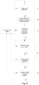
- a method of preventing fraud in accordance with the apparatus and operations described above, is detailed below in relation to figure 6 .
- the controller 8 of the fraud prevention apparatus 1 is configured to detect a trigger event which indicates that the operating frequency of the oscillating sensor 3a should be changed.
- the trigger event may be the elapse of a predetermined time period since a previous event, or the detection or occurrence of a particular event as previously described.
- the controller 8 is configured to cause the change in the operating frequency of the sensor 3a, for example by altering the configuration of the oscillator circuit.
- the controller 8 of the fraud prevention apparatus 1 is configured to check whether the operating frequency of the sensor 3a has changed as expected and, if it has not, may be configured to cause a fraud alarm signal to be generated.
- a fourth step S4 in response to detection of an object in the coin outlet path 5 by one or both of the separately located coin sensors 3a, 3b, the controller 8 is configured to determine the direction in which the object has moved along the outlet path 5 by determining the order in which the object was detected by the sensors 3a, 3b. If the direction of travel is not as expected, the controller 8 may be configured to cause the fraud alarm signal to be generated.
- the controller 8 is configured to determine whether a measured time gap between the object being independently detected by the coin sensors 3a, 3b is as would be expected for a coin being dispensed from the coin storage 6 under normal operating conditions. If the time gap is not as expected, the controller 8 may be configured to cause the fraud alarm signal to be generated.
- the oscillator illustrated in the figures is for a Frequency Modulation (FM) sensor
- the oscillating sensor 3a could alternatively comprise an FM and Amplitude Modulation (AM) sensor as an additional layer of security.
- AM Amplitude Modulation
- a demodulated AM signal would provide an analogue signal to the controller 8 which is responsible for causing changes in the expected oscillating frequency of the sensor 3a.
- the controller 8 would be configured to determine changes in the FM and AM signals output by the sensor 3a and to verify that the changes, for example from a default value, are in one direction only until a peak signal is received, followed by changes in the opposite direction, for example back to the default value.
- the peak values in the output signals may occur when the coin is centrally located in or adjacent the coin sensing element 7. Changes in signal direction which occur at an unexpected time, such as one which does not correspond to the peak signal deviation from the default value, may be indicative of a fraud attack.
- the controller 8 may also be configured to determine the magnitude of the peak signal deviations and to verify that the magnitudes fall within expected limits, which may be stored in the memory 10.
- a high Quality Factor circuit design ensures a relatively large variation in AM signal for a small change in the oscillating frequency of the sensor 3a and thus puts in place an extra variable that a would-be fraudster must attempt to manipulate when making a fraud attack.
- Such a design would also provide a high level of variation in the operational (e.g. frequency) characteristics of the sensor 3a for relatively small changes in component values, thus adding to the complexity and difficulty of successfully manipulating a plurality of sensors 3a in the same manner.
- oscillator circuit is described above principally in relation to an LC oscillator, other types of oscillator could alternatively be used.
- the oscillating frequencies of such alternative oscillators can be varied by altering the component configuration of the oscillator in a similar manner to the LC examples.
- a specific example of an alternative oscillator is an RL or RC oscillator, in which a resistance value of the circuit is varied under the control of the controller 8 to cause a change in the oscillating frequency of the sensor 3a.
- Resistive components such as one or more resistors can be switched in and out of the circuit in a similar manner to capacitive components in order to alter the oscillating frequency.
- the verification operation for the oscillating sensor 3a may comprise altering the resistance of an RL or RC oscillator in the sensor 3a by a known amount and subsequently verifying that the oscillating frequency of the sensor 3a has changed as would be expected following the known change in resistance.
- the resistance may be altered by replacing, adding and/or removing resistive components to/from the oscillator circuit.
- the senor 3a may be selectively coupled to a plurality of resistors which can be selectively switched into and out of the oscillator by the controller 8, for example using one or more switches 12 as described previously or by applying control signals to the components from the controller 8.
- the controller 8 may be configured to adjust the values of variable components in the oscillator, such as one or more variable resistors, in order to alter the oscillating frequency of the sensor 3a.
Landscapes
- Physics & Mathematics (AREA)
- General Physics & Mathematics (AREA)
- Control Of Vending Devices And Auxiliary Devices For Vending Devices (AREA)
- Slot Machines And Peripheral Devices (AREA)
- Testing Of Coins (AREA)
Applications Claiming Priority (2)
| Application Number | Priority Date | Filing Date | Title |
|---|---|---|---|
| GB1221504.2A GB2508377A (en) | 2012-11-29 | 2012-11-29 | Preventing fraud in a coin payout mechanism |
| PCT/GB2013/053080 WO2014083319A1 (en) | 2012-11-29 | 2013-11-22 | Preventing fraud |
Publications (2)
| Publication Number | Publication Date |
|---|---|
| EP2926322A1 EP2926322A1 (en) | 2015-10-07 |
| EP2926322B1 true EP2926322B1 (en) | 2024-06-19 |
Family
ID=49674343
Family Applications (1)
| Application Number | Title | Priority Date | Filing Date |
|---|---|---|---|
| EP13796144.7A Active EP2926322B1 (en) | 2012-11-29 | 2013-11-22 | Preventing fraud |
Country Status (7)
Citations (2)
| Publication number | Priority date | Publication date | Assignee | Title |
|---|---|---|---|---|
| US4579217A (en) * | 1983-06-06 | 1986-04-01 | Coin Controls Limited | Electronic coin validator |
| WO2002077932A1 (en) * | 2001-03-22 | 2002-10-03 | Scan Coin Industries Ab | A coin discriminating device and method, and a coin handling machine including such a device and method |
Family Cites Families (11)
| Publication number | Priority date | Publication date | Assignee | Title |
|---|---|---|---|---|
| GB1452740A (en) * | 1972-10-12 | 1976-10-13 | Mars Inc | Digital memory coin selector method and apparatus |
| JPS586191B2 (ja) * | 1976-04-23 | 1983-02-03 | 株式会社日本コインコ | 自動販売機の硬貨受入装置 |
| DE2821685A1 (de) * | 1978-05-18 | 1979-11-22 | Georg Pruemm | Verfahren zur verringerung des falschgeldrisikos beim betrieb muenzbetaetigter automaten und muenzpruefer zur durchfuehrung des verfahrens |
| GB9010507D0 (en) * | 1990-05-10 | 1990-07-04 | Mars Inc | Apparatus and method for testing coins |
| US5568854A (en) * | 1991-06-28 | 1996-10-29 | Protel, Inc. | Coin discrimination method |
| US5531309A (en) * | 1995-08-28 | 1996-07-02 | Bally Gaming International, Inc. | Method and apparatus for detecting fraud or theft in a gaming machine |
| GB0023165D0 (en) * | 2000-09-20 | 2000-11-01 | Igt Uk Ltd | Coin dispensing mechanism |
| US6920972B2 (en) * | 2002-02-01 | 2005-07-26 | Pom, Incorporated | Coin fraud detection sensing system and method |
| JP2005312889A (ja) * | 2004-04-02 | 2005-11-10 | Aruze Corp | コイン送出装置及び遊技機 |
| WO2010052798A1 (ja) * | 2008-11-10 | 2010-05-14 | グローリー株式会社 | 硬貨識別装置および硬貨識別方法 |
| US8496171B2 (en) * | 2011-05-03 | 2013-07-30 | Ncr Corporation | Fraud prevention |
-
2012
- 2012-11-29 GB GB1221504.2A patent/GB2508377A/en not_active Withdrawn
-
2013
- 2013-11-22 AU AU2013350949A patent/AU2013350949B2/en active Active
- 2013-11-22 JP JP2015544528A patent/JP6377627B2/ja not_active Expired - Fee Related
- 2013-11-22 EP EP13796144.7A patent/EP2926322B1/en active Active
- 2013-11-22 WO PCT/GB2013/053080 patent/WO2014083319A1/en active Application Filing
- 2013-11-22 ES ES13796144T patent/ES2984174T3/es active Active
- 2013-11-22 CN CN201380062395.1A patent/CN104838427B/zh active Active
Patent Citations (2)
| Publication number | Priority date | Publication date | Assignee | Title |
|---|---|---|---|---|
| US4579217A (en) * | 1983-06-06 | 1986-04-01 | Coin Controls Limited | Electronic coin validator |
| WO2002077932A1 (en) * | 2001-03-22 | 2002-10-03 | Scan Coin Industries Ab | A coin discriminating device and method, and a coin handling machine including such a device and method |
Also Published As
| Publication number | Publication date |
|---|---|
| CN104838427A (zh) | 2015-08-12 |
| WO2014083319A1 (en) | 2014-06-05 |
| JP2016502197A (ja) | 2016-01-21 |
| ES2984174T3 (es) | 2024-10-29 |
| AU2013350949B2 (en) | 2017-09-07 |
| AU2013350949A1 (en) | 2015-04-09 |
| CN104838427B (zh) | 2017-07-28 |
| EP2926322A1 (en) | 2015-10-07 |
| GB2508377A (en) | 2014-06-04 |
| JP6377627B2 (ja) | 2018-08-22 |
Similar Documents
| Publication | Publication Date | Title |
|---|---|---|
| US4184366A (en) | Coin testing apparatus | |
| US4646904A (en) | Coin sizing means and method | |
| EP0560827B1 (en) | Money validators | |
| JPH09509771A (ja) | 硬貨を識別する方法及びその装置 | |
| EP0308997B1 (en) | Coin validators | |
| EP0781421A1 (en) | Vehicle detector system with periodic source filtering | |
| AU768811B2 (en) | Money item acceptor | |
| EP2926322B1 (en) | Preventing fraud | |
| AU688982B2 (en) | Vehicle detector system | |
| US7490709B2 (en) | Coin discriminating device and method, and a coin handling machine including such a device and method | |
| US5526918A (en) | Coin validating apparatus and method | |
| JP5316768B2 (ja) | スロットマシン及びメダル検出装置 | |
| US5060778A (en) | Moving coin validation | |
| US20040155650A1 (en) | Verification method | |
| EP0880757B1 (en) | Coin diameter measurement | |
| JP2009045381A (ja) | 遊技機の不正状態検出方法、不正状態検出装置及び不正状態検出用計数器 | |
| KR100666030B1 (ko) | 고속동전계수장치 | |
| JP2000348232A (ja) | 硬貨識別装置 | |
| GB1576714A (en) | Coin testing apparatus | |
| JP2011235196A (ja) | ゲーム機 |
Legal Events
| Date | Code | Title | Description |
|---|---|---|---|
| PUAI | Public reference made under article 153(3) epc to a published international application that has entered the european phase |
Free format text: ORIGINAL CODE: 0009012 |
|
| 17P | Request for examination filed |
Effective date: 20150312 |
|
| AK | Designated contracting states |
Kind code of ref document: A1 Designated state(s): AL AT BE BG CH CY CZ DE DK EE ES FI FR GB GR HR HU IE IS IT LI LT LU LV MC MK MT NL NO PL PT RO RS SE SI SK SM TR |
|
| AX | Request for extension of the european patent |
Extension state: BA ME |
|
| DAX | Request for extension of the european patent (deleted) | ||
| RAP1 | Party data changed (applicant data changed or rights of an application transferred) |
Owner name: CRANE PAYMENT INNOVATIONS LIMITED |
|
| STAA | Information on the status of an ep patent application or granted ep patent |
Free format text: STATUS: EXAMINATION IS IN PROGRESS |
|
| 17Q | First examination report despatched |
Effective date: 20210323 |
|
| STAA | Information on the status of an ep patent application or granted ep patent |
Free format text: STATUS: EXAMINATION IS IN PROGRESS |
|
| GRAP | Despatch of communication of intention to grant a patent |
Free format text: ORIGINAL CODE: EPIDOSNIGR1 |
|
| STAA | Information on the status of an ep patent application or granted ep patent |
Free format text: STATUS: GRANT OF PATENT IS INTENDED |
|
| INTG | Intention to grant announced |
Effective date: 20240115 |
|
| GRAS | Grant fee paid |
Free format text: ORIGINAL CODE: EPIDOSNIGR3 |
|
| GRAA | (expected) grant |
Free format text: ORIGINAL CODE: 0009210 |
|
| STAA | Information on the status of an ep patent application or granted ep patent |
Free format text: STATUS: THE PATENT HAS BEEN GRANTED |
|
| AK | Designated contracting states |
Kind code of ref document: B1 Designated state(s): AL AT BE BG CH CY CZ DE DK EE ES FI FR GB GR HR HU IE IS IT LI LT LU LV MC MK MT NL NO PL PT RO RS SE SI SK SM TR |
|
| REG | Reference to a national code |
Ref country code: GB Ref legal event code: FG4D |
|
| REG | Reference to a national code |
Ref country code: CH Ref legal event code: EP |
|
| REG | Reference to a national code |
Ref country code: DE Ref legal event code: R096 Ref document number: 602013085820 Country of ref document: DE |
|
| P01 | Opt-out of the competence of the unified patent court (upc) registered |
Free format text: CASE NUMBER: APP_33914/2024 Effective date: 20240606 |
|
| PG25 | Lapsed in a contracting state [announced via postgrant information from national office to epo] |
Ref country code: BG Free format text: LAPSE BECAUSE OF FAILURE TO SUBMIT A TRANSLATION OF THE DESCRIPTION OR TO PAY THE FEE WITHIN THE PRESCRIBED TIME-LIMIT Effective date: 20240619 |
|
| PG25 | Lapsed in a contracting state [announced via postgrant information from national office to epo] |
Ref country code: HR Free format text: LAPSE BECAUSE OF FAILURE TO SUBMIT A TRANSLATION OF THE DESCRIPTION OR TO PAY THE FEE WITHIN THE PRESCRIBED TIME-LIMIT Effective date: 20240619 Ref country code: FI Free format text: LAPSE BECAUSE OF FAILURE TO SUBMIT A TRANSLATION OF THE DESCRIPTION OR TO PAY THE FEE WITHIN THE PRESCRIBED TIME-LIMIT Effective date: 20240619 |
|
| REG | Reference to a national code |
Ref country code: LT Ref legal event code: MG9D |
|
| PG25 | Lapsed in a contracting state [announced via postgrant information from national office to epo] |
Ref country code: GR Free format text: LAPSE BECAUSE OF FAILURE TO SUBMIT A TRANSLATION OF THE DESCRIPTION OR TO PAY THE FEE WITHIN THE PRESCRIBED TIME-LIMIT Effective date: 20240920 |
|
| REG | Reference to a national code |
Ref country code: NL Ref legal event code: MP Effective date: 20240619 |
|
| REG | Reference to a national code |
Ref country code: ES Ref legal event code: FG2A Ref document number: 2984174 Country of ref document: ES Kind code of ref document: T3 Effective date: 20241029 |
|
| PG25 | Lapsed in a contracting state [announced via postgrant information from national office to epo] |
Ref country code: LV Free format text: LAPSE BECAUSE OF FAILURE TO SUBMIT A TRANSLATION OF THE DESCRIPTION OR TO PAY THE FEE WITHIN THE PRESCRIBED TIME-LIMIT Effective date: 20240619 |
|
| PG25 | Lapsed in a contracting state [announced via postgrant information from national office to epo] |
Ref country code: NO Free format text: LAPSE BECAUSE OF FAILURE TO SUBMIT A TRANSLATION OF THE DESCRIPTION OR TO PAY THE FEE WITHIN THE PRESCRIBED TIME-LIMIT Effective date: 20240919 Ref country code: LV Free format text: LAPSE BECAUSE OF FAILURE TO SUBMIT A TRANSLATION OF THE DESCRIPTION OR TO PAY THE FEE WITHIN THE PRESCRIBED TIME-LIMIT Effective date: 20240619 Ref country code: HR Free format text: LAPSE BECAUSE OF FAILURE TO SUBMIT A TRANSLATION OF THE DESCRIPTION OR TO PAY THE FEE WITHIN THE PRESCRIBED TIME-LIMIT Effective date: 20240619 Ref country code: GR Free format text: LAPSE BECAUSE OF FAILURE TO SUBMIT A TRANSLATION OF THE DESCRIPTION OR TO PAY THE FEE WITHIN THE PRESCRIBED TIME-LIMIT Effective date: 20240920 Ref country code: FI Free format text: LAPSE BECAUSE OF FAILURE TO SUBMIT A TRANSLATION OF THE DESCRIPTION OR TO PAY THE FEE WITHIN THE PRESCRIBED TIME-LIMIT Effective date: 20240619 Ref country code: BG Free format text: LAPSE BECAUSE OF FAILURE TO SUBMIT A TRANSLATION OF THE DESCRIPTION OR TO PAY THE FEE WITHIN THE PRESCRIBED TIME-LIMIT Effective date: 20240619 Ref country code: RS Free format text: LAPSE BECAUSE OF FAILURE TO SUBMIT A TRANSLATION OF THE DESCRIPTION OR TO PAY THE FEE WITHIN THE PRESCRIBED TIME-LIMIT Effective date: 20240919 |
|
| PG25 | Lapsed in a contracting state [announced via postgrant information from national office to epo] |
Ref country code: NL Free format text: LAPSE BECAUSE OF FAILURE TO SUBMIT A TRANSLATION OF THE DESCRIPTION OR TO PAY THE FEE WITHIN THE PRESCRIBED TIME-LIMIT Effective date: 20240619 |
|
| REG | Reference to a national code |
Ref country code: AT Ref legal event code: MK05 Ref document number: 1696437 Country of ref document: AT Kind code of ref document: T Effective date: 20240619 |
|
| PG25 | Lapsed in a contracting state [announced via postgrant information from national office to epo] |
Ref country code: NL Free format text: LAPSE BECAUSE OF FAILURE TO SUBMIT A TRANSLATION OF THE DESCRIPTION OR TO PAY THE FEE WITHIN THE PRESCRIBED TIME-LIMIT Effective date: 20240619 |
|
| PG25 | Lapsed in a contracting state [announced via postgrant information from national office to epo] |
Ref country code: PT Free format text: LAPSE BECAUSE OF FAILURE TO SUBMIT A TRANSLATION OF THE DESCRIPTION OR TO PAY THE FEE WITHIN THE PRESCRIBED TIME-LIMIT Effective date: 20241021 |
|
| PG25 | Lapsed in a contracting state [announced via postgrant information from national office to epo] |
Ref country code: PT Free format text: LAPSE BECAUSE OF FAILURE TO SUBMIT A TRANSLATION OF THE DESCRIPTION OR TO PAY THE FEE WITHIN THE PRESCRIBED TIME-LIMIT Effective date: 20241021 |
|
| PGFP | Annual fee paid to national office [announced via postgrant information from national office to epo] |
Ref country code: DE Payment date: 20240925 Year of fee payment: 12 |
|
| PG25 | Lapsed in a contracting state [announced via postgrant information from national office to epo] |
Ref country code: PL Free format text: LAPSE BECAUSE OF FAILURE TO SUBMIT A TRANSLATION OF THE DESCRIPTION OR TO PAY THE FEE WITHIN THE PRESCRIBED TIME-LIMIT Effective date: 20240619 |
|
| PGFP | Annual fee paid to national office [announced via postgrant information from national office to epo] |
Ref country code: GB Payment date: 20241001 Year of fee payment: 12 |
|
| PG25 | Lapsed in a contracting state [announced via postgrant information from national office to epo] |
Ref country code: EE Free format text: LAPSE BECAUSE OF FAILURE TO SUBMIT A TRANSLATION OF THE DESCRIPTION OR TO PAY THE FEE WITHIN THE PRESCRIBED TIME-LIMIT Effective date: 20240619 |
|
| PG25 | Lapsed in a contracting state [announced via postgrant information from national office to epo] |
Ref country code: IS Free format text: LAPSE BECAUSE OF FAILURE TO SUBMIT A TRANSLATION OF THE DESCRIPTION OR TO PAY THE FEE WITHIN THE PRESCRIBED TIME-LIMIT Effective date: 20241019 Ref country code: AT Free format text: LAPSE BECAUSE OF FAILURE TO SUBMIT A TRANSLATION OF THE DESCRIPTION OR TO PAY THE FEE WITHIN THE PRESCRIBED TIME-LIMIT Effective date: 20240619 |
|
| PG25 | Lapsed in a contracting state [announced via postgrant information from national office to epo] |
Ref country code: CZ Free format text: LAPSE BECAUSE OF FAILURE TO SUBMIT A TRANSLATION OF THE DESCRIPTION OR TO PAY THE FEE WITHIN THE PRESCRIBED TIME-LIMIT Effective date: 20240619 |
|
| PG25 | Lapsed in a contracting state [announced via postgrant information from national office to epo] |
Ref country code: SK Free format text: LAPSE BECAUSE OF FAILURE TO SUBMIT A TRANSLATION OF THE DESCRIPTION OR TO PAY THE FEE WITHIN THE PRESCRIBED TIME-LIMIT Effective date: 20240619 Ref country code: RO Free format text: LAPSE BECAUSE OF FAILURE TO SUBMIT A TRANSLATION OF THE DESCRIPTION OR TO PAY THE FEE WITHIN THE PRESCRIBED TIME-LIMIT Effective date: 20240619 |
|
| PG25 | Lapsed in a contracting state [announced via postgrant information from national office to epo] |
Ref country code: SM Free format text: LAPSE BECAUSE OF FAILURE TO SUBMIT A TRANSLATION OF THE DESCRIPTION OR TO PAY THE FEE WITHIN THE PRESCRIBED TIME-LIMIT Effective date: 20240619 |
|
| PGFP | Annual fee paid to national office [announced via postgrant information from national office to epo] |
Ref country code: IT Payment date: 20241010 Year of fee payment: 12 Ref country code: ES Payment date: 20241206 Year of fee payment: 12 |
|
| PG25 | Lapsed in a contracting state [announced via postgrant information from national office to epo] |
Ref country code: SM Free format text: LAPSE BECAUSE OF FAILURE TO SUBMIT A TRANSLATION OF THE DESCRIPTION OR TO PAY THE FEE WITHIN THE PRESCRIBED TIME-LIMIT Effective date: 20240619 Ref country code: SK Free format text: LAPSE BECAUSE OF FAILURE TO SUBMIT A TRANSLATION OF THE DESCRIPTION OR TO PAY THE FEE WITHIN THE PRESCRIBED TIME-LIMIT Effective date: 20240619 Ref country code: RO Free format text: LAPSE BECAUSE OF FAILURE TO SUBMIT A TRANSLATION OF THE DESCRIPTION OR TO PAY THE FEE WITHIN THE PRESCRIBED TIME-LIMIT Effective date: 20240619 Ref country code: PL Free format text: LAPSE BECAUSE OF FAILURE TO SUBMIT A TRANSLATION OF THE DESCRIPTION OR TO PAY THE FEE WITHIN THE PRESCRIBED TIME-LIMIT Effective date: 20240619 Ref country code: IS Free format text: LAPSE BECAUSE OF FAILURE TO SUBMIT A TRANSLATION OF THE DESCRIPTION OR TO PAY THE FEE WITHIN THE PRESCRIBED TIME-LIMIT Effective date: 20241019 Ref country code: EE Free format text: LAPSE BECAUSE OF FAILURE TO SUBMIT A TRANSLATION OF THE DESCRIPTION OR TO PAY THE FEE WITHIN THE PRESCRIBED TIME-LIMIT Effective date: 20240619 Ref country code: CZ Free format text: LAPSE BECAUSE OF FAILURE TO SUBMIT A TRANSLATION OF THE DESCRIPTION OR TO PAY THE FEE WITHIN THE PRESCRIBED TIME-LIMIT Effective date: 20240619 Ref country code: AT Free format text: LAPSE BECAUSE OF FAILURE TO SUBMIT A TRANSLATION OF THE DESCRIPTION OR TO PAY THE FEE WITHIN THE PRESCRIBED TIME-LIMIT Effective date: 20240619 |
|
| REG | Reference to a national code |
Ref country code: DE Ref legal event code: R097 Ref document number: 602013085820 Country of ref document: DE |
|
| PG25 | Lapsed in a contracting state [announced via postgrant information from national office to epo] |
Ref country code: DK Free format text: LAPSE BECAUSE OF FAILURE TO SUBMIT A TRANSLATION OF THE DESCRIPTION OR TO PAY THE FEE WITHIN THE PRESCRIBED TIME-LIMIT Effective date: 20240619 |
|
| PLBE | No opposition filed within time limit |
Free format text: ORIGINAL CODE: 0009261 |
|
| STAA | Information on the status of an ep patent application or granted ep patent |
Free format text: STATUS: NO OPPOSITION FILED WITHIN TIME LIMIT |
|
| 26N | No opposition filed |
Effective date: 20250320 |
|
| REG | Reference to a national code |
Ref country code: CH Ref legal event code: PL |
|
| PG25 | Lapsed in a contracting state [announced via postgrant information from national office to epo] |
Ref country code: MC Free format text: LAPSE BECAUSE OF FAILURE TO SUBMIT A TRANSLATION OF THE DESCRIPTION OR TO PAY THE FEE WITHIN THE PRESCRIBED TIME-LIMIT Effective date: 20240619 |
|
| PG25 | Lapsed in a contracting state [announced via postgrant information from national office to epo] |
Ref country code: LU Free format text: LAPSE BECAUSE OF NON-PAYMENT OF DUE FEES Effective date: 20241122 |
|
| REG | Reference to a national code |
Ref country code: CH Ref legal event code: PL |
|
| PG25 | Lapsed in a contracting state [announced via postgrant information from national office to epo] |
Ref country code: CH Free format text: LAPSE BECAUSE OF NON-PAYMENT OF DUE FEES Effective date: 20241130 |