EP2924728B1 - Bondfläche für eine Halbleiteranordnung und entsprechendes Verfahren - Google Patents
Bondfläche für eine Halbleiteranordnung und entsprechendes Verfahren Download PDFInfo
- Publication number
- EP2924728B1 EP2924728B1 EP15160048.3A EP15160048A EP2924728B1 EP 2924728 B1 EP2924728 B1 EP 2924728B1 EP 15160048 A EP15160048 A EP 15160048A EP 2924728 B1 EP2924728 B1 EP 2924728B1
- Authority
- EP
- European Patent Office
- Prior art keywords
- shelf
- substrate layer
- planar surface
- attach pad
- top planar
- Prior art date
- Legal status (The legal status is an assumption and is not a legal conclusion. Google has not performed a legal analysis and makes no representation as to the accuracy of the status listed.)
- Not-in-force
Links
Images





Classifications
-
- H—ELECTRICITY
- H10—SEMICONDUCTOR DEVICES; ELECTRIC SOLID-STATE DEVICES NOT OTHERWISE PROVIDED FOR
- H10F—INORGANIC SEMICONDUCTOR DEVICES SENSITIVE TO INFRARED RADIATION, LIGHT, ELECTROMAGNETIC RADIATION OF SHORTER WAVELENGTH OR CORPUSCULAR RADIATION
- H10F39/00—Integrated devices, or assemblies of multiple devices, comprising at least one element covered by group H10F30/00, e.g. radiation detectors comprising photodiode arrays
- H10F39/80—Constructional details of image sensors
- H10F39/809—Constructional details of image sensors of hybrid image sensors
-
- H—ELECTRICITY
- H10—SEMICONDUCTOR DEVICES; ELECTRIC SOLID-STATE DEVICES NOT OTHERWISE PROVIDED FOR
- H10F—INORGANIC SEMICONDUCTOR DEVICES SENSITIVE TO INFRARED RADIATION, LIGHT, ELECTROMAGNETIC RADIATION OF SHORTER WAVELENGTH OR CORPUSCULAR RADIATION
- H10F39/00—Integrated devices, or assemblies of multiple devices, comprising at least one element covered by group H10F30/00, e.g. radiation detectors comprising photodiode arrays
- H10F39/011—Manufacture or treatment of image sensors covered by group H10F39/12
- H10F39/018—Manufacture or treatment of image sensors covered by group H10F39/12 of hybrid image sensors
-
- H—ELECTRICITY
- H10—SEMICONDUCTOR DEVICES; ELECTRIC SOLID-STATE DEVICES NOT OTHERWISE PROVIDED FOR
- H10W—GENERIC PACKAGES, INTERCONNECTIONS, CONNECTORS OR OTHER CONSTRUCTIONAL DETAILS OF DEVICES COVERED BY CLASS H10
- H10W90/00—Package configurations
- H10W90/20—Configurations of stacked chips
- H10W90/28—Configurations of stacked chips the stacked chips having different sizes, e.g. chip stacks having a pyramidal shape
-
- H—ELECTRICITY
- H10—SEMICONDUCTOR DEVICES; ELECTRIC SOLID-STATE DEVICES NOT OTHERWISE PROVIDED FOR
- H10W—GENERIC PACKAGES, INTERCONNECTIONS, CONNECTORS OR OTHER CONSTRUCTIONAL DETAILS OF DEVICES COVERED BY CLASS H10
- H10W70/00—Package substrates; Interposers; Redistribution layers [RDL]
- H10W70/60—Insulating or insulated package substrates; Interposers; Redistribution layers
- H10W70/62—Insulating or insulated package substrates; Interposers; Redistribution layers characterised by their interconnections
- H10W70/65—Shapes or dispositions of interconnections
-
- H—ELECTRICITY
- H10—SEMICONDUCTOR DEVICES; ELECTRIC SOLID-STATE DEVICES NOT OTHERWISE PROVIDED FOR
- H10W—GENERIC PACKAGES, INTERCONNECTIONS, CONNECTORS OR OTHER CONSTRUCTIONAL DETAILS OF DEVICES COVERED BY CLASS H10
- H10W72/00—Interconnections or connectors in packages
- H10W72/071—Connecting or disconnecting
- H10W72/075—Connecting or disconnecting of bond wires
- H10W72/07521—Aligning
-
- H—ELECTRICITY
- H10—SEMICONDUCTOR DEVICES; ELECTRIC SOLID-STATE DEVICES NOT OTHERWISE PROVIDED FOR
- H10W—GENERIC PACKAGES, INTERCONNECTIONS, CONNECTORS OR OTHER CONSTRUCTIONAL DETAILS OF DEVICES COVERED BY CLASS H10
- H10W72/00—Interconnections or connectors in packages
- H10W72/071—Connecting or disconnecting
- H10W72/075—Connecting or disconnecting of bond wires
- H10W72/07531—Techniques
- H10W72/07532—Compression bonding, e.g. thermocompression bonding
-
- H—ELECTRICITY
- H10—SEMICONDUCTOR DEVICES; ELECTRIC SOLID-STATE DEVICES NOT OTHERWISE PROVIDED FOR
- H10W—GENERIC PACKAGES, INTERCONNECTIONS, CONNECTORS OR OTHER CONSTRUCTIONAL DETAILS OF DEVICES COVERED BY CLASS H10
- H10W72/00—Interconnections or connectors in packages
- H10W72/071—Connecting or disconnecting
- H10W72/075—Connecting or disconnecting of bond wires
- H10W72/07531—Techniques
- H10W72/07532—Compression bonding, e.g. thermocompression bonding
- H10W72/07533—Ultrasonic bonding, e.g. thermosonic bonding
-
- H—ELECTRICITY
- H10—SEMICONDUCTOR DEVICES; ELECTRIC SOLID-STATE DEVICES NOT OTHERWISE PROVIDED FOR
- H10W—GENERIC PACKAGES, INTERCONNECTIONS, CONNECTORS OR OTHER CONSTRUCTIONAL DETAILS OF DEVICES COVERED BY CLASS H10
- H10W72/00—Interconnections or connectors in packages
- H10W72/071—Connecting or disconnecting
- H10W72/075—Connecting or disconnecting of bond wires
- H10W72/07551—Connecting or disconnecting of bond wires characterised by changes in properties of the bond wires during the connecting
- H10W72/07553—Connecting or disconnecting of bond wires characterised by changes in properties of the bond wires during the connecting changes in shapes
-
- H—ELECTRICITY
- H10—SEMICONDUCTOR DEVICES; ELECTRIC SOLID-STATE DEVICES NOT OTHERWISE PROVIDED FOR
- H10W—GENERIC PACKAGES, INTERCONNECTIONS, CONNECTORS OR OTHER CONSTRUCTIONAL DETAILS OF DEVICES COVERED BY CLASS H10
- H10W72/00—Interconnections or connectors in packages
- H10W72/071—Connecting or disconnecting
- H10W72/075—Connecting or disconnecting of bond wires
- H10W72/07551—Connecting or disconnecting of bond wires characterised by changes in properties of the bond wires during the connecting
- H10W72/07554—Connecting or disconnecting of bond wires characterised by changes in properties of the bond wires during the connecting changes in dispositions
-
- H—ELECTRICITY
- H10—SEMICONDUCTOR DEVICES; ELECTRIC SOLID-STATE DEVICES NOT OTHERWISE PROVIDED FOR
- H10W—GENERIC PACKAGES, INTERCONNECTIONS, CONNECTORS OR OTHER CONSTRUCTIONAL DETAILS OF DEVICES COVERED BY CLASS H10
- H10W72/00—Interconnections or connectors in packages
- H10W72/50—Bond wires
- H10W72/531—Shapes of wire connectors
-
- H—ELECTRICITY
- H10—SEMICONDUCTOR DEVICES; ELECTRIC SOLID-STATE DEVICES NOT OTHERWISE PROVIDED FOR
- H10W—GENERIC PACKAGES, INTERCONNECTIONS, CONNECTORS OR OTHER CONSTRUCTIONAL DETAILS OF DEVICES COVERED BY CLASS H10
- H10W72/00—Interconnections or connectors in packages
- H10W72/50—Bond wires
- H10W72/531—Shapes of wire connectors
- H10W72/536—Shapes of wire connectors the connected ends being ball-shaped
-
- H—ELECTRICITY
- H10—SEMICONDUCTOR DEVICES; ELECTRIC SOLID-STATE DEVICES NOT OTHERWISE PROVIDED FOR
- H10W—GENERIC PACKAGES, INTERCONNECTIONS, CONNECTORS OR OTHER CONSTRUCTIONAL DETAILS OF DEVICES COVERED BY CLASS H10
- H10W72/00—Interconnections or connectors in packages
- H10W72/50—Bond wires
- H10W72/531—Shapes of wire connectors
- H10W72/5363—Shapes of wire connectors the connected ends being wedge-shaped
-
- H—ELECTRICITY
- H10—SEMICONDUCTOR DEVICES; ELECTRIC SOLID-STATE DEVICES NOT OTHERWISE PROVIDED FOR
- H10W—GENERIC PACKAGES, INTERCONNECTIONS, CONNECTORS OR OTHER CONSTRUCTIONAL DETAILS OF DEVICES COVERED BY CLASS H10
- H10W72/00—Interconnections or connectors in packages
- H10W72/50—Bond wires
- H10W72/541—Dispositions of bond wires
- H10W72/5449—Dispositions of bond wires not being orthogonal to a side surface of the chip, e.g. fan-out arrangements
-
- H—ELECTRICITY
- H10—SEMICONDUCTOR DEVICES; ELECTRIC SOLID-STATE DEVICES NOT OTHERWISE PROVIDED FOR
- H10W—GENERIC PACKAGES, INTERCONNECTIONS, CONNECTORS OR OTHER CONSTRUCTIONAL DETAILS OF DEVICES COVERED BY CLASS H10
- H10W72/00—Interconnections or connectors in packages
- H10W72/50—Bond wires
- H10W72/551—Materials of bond wires
- H10W72/552—Materials of bond wires comprising metals or metalloids, e.g. silver
- H10W72/5522—Materials of bond wires comprising metals or metalloids, e.g. silver comprising gold [Au]
-
- H—ELECTRICITY
- H10—SEMICONDUCTOR DEVICES; ELECTRIC SOLID-STATE DEVICES NOT OTHERWISE PROVIDED FOR
- H10W—GENERIC PACKAGES, INTERCONNECTIONS, CONNECTORS OR OTHER CONSTRUCTIONAL DETAILS OF DEVICES COVERED BY CLASS H10
- H10W72/00—Interconnections or connectors in packages
- H10W72/50—Bond wires
- H10W72/551—Materials of bond wires
- H10W72/552—Materials of bond wires comprising metals or metalloids, e.g. silver
- H10W72/5524—Materials of bond wires comprising metals or metalloids, e.g. silver comprising aluminium [Al]
-
- H—ELECTRICITY
- H10—SEMICONDUCTOR DEVICES; ELECTRIC SOLID-STATE DEVICES NOT OTHERWISE PROVIDED FOR
- H10W—GENERIC PACKAGES, INTERCONNECTIONS, CONNECTORS OR OTHER CONSTRUCTIONAL DETAILS OF DEVICES COVERED BY CLASS H10
- H10W72/00—Interconnections or connectors in packages
- H10W72/50—Bond wires
- H10W72/551—Materials of bond wires
- H10W72/552—Materials of bond wires comprising metals or metalloids, e.g. silver
- H10W72/5525—Materials of bond wires comprising metals or metalloids, e.g. silver comprising copper [Cu]
-
- H—ELECTRICITY
- H10—SEMICONDUCTOR DEVICES; ELECTRIC SOLID-STATE DEVICES NOT OTHERWISE PROVIDED FOR
- H10W—GENERIC PACKAGES, INTERCONNECTIONS, CONNECTORS OR OTHER CONSTRUCTIONAL DETAILS OF DEVICES COVERED BY CLASS H10
- H10W72/00—Interconnections or connectors in packages
- H10W72/50—Bond wires
- H10W72/59—Bond pads specially adapted therefor
-
- H—ELECTRICITY
- H10—SEMICONDUCTOR DEVICES; ELECTRIC SOLID-STATE DEVICES NOT OTHERWISE PROVIDED FOR
- H10W—GENERIC PACKAGES, INTERCONNECTIONS, CONNECTORS OR OTHER CONSTRUCTIONAL DETAILS OF DEVICES COVERED BY CLASS H10
- H10W72/00—Interconnections or connectors in packages
- H10W72/90—Bond pads, in general
- H10W72/921—Structures or relative sizes of bond pads
- H10W72/922—Bond pads being integral with underlying chip-level interconnections
-
- H—ELECTRICITY
- H10—SEMICONDUCTOR DEVICES; ELECTRIC SOLID-STATE DEVICES NOT OTHERWISE PROVIDED FOR
- H10W—GENERIC PACKAGES, INTERCONNECTIONS, CONNECTORS OR OTHER CONSTRUCTIONAL DETAILS OF DEVICES COVERED BY CLASS H10
- H10W72/00—Interconnections or connectors in packages
- H10W72/90—Bond pads, in general
- H10W72/931—Shapes of bond pads
- H10W72/932—Plan-view shape, i.e. in top view
-
- H—ELECTRICITY
- H10—SEMICONDUCTOR DEVICES; ELECTRIC SOLID-STATE DEVICES NOT OTHERWISE PROVIDED FOR
- H10W—GENERIC PACKAGES, INTERCONNECTIONS, CONNECTORS OR OTHER CONSTRUCTIONAL DETAILS OF DEVICES COVERED BY CLASS H10
- H10W72/00—Interconnections or connectors in packages
- H10W72/90—Bond pads, in general
- H10W72/941—Dispositions of bond pads
- H10W72/9415—Dispositions of bond pads relative to the surface, e.g. recessed, protruding
-
- H—ELECTRICITY
- H10—SEMICONDUCTOR DEVICES; ELECTRIC SOLID-STATE DEVICES NOT OTHERWISE PROVIDED FOR
- H10W—GENERIC PACKAGES, INTERCONNECTIONS, CONNECTORS OR OTHER CONSTRUCTIONAL DETAILS OF DEVICES COVERED BY CLASS H10
- H10W90/00—Package configurations
- H10W90/701—Package configurations characterised by the relative positions of pads or connectors relative to package parts
- H10W90/751—Package configurations characterised by the relative positions of pads or connectors relative to package parts of bond wires
- H10W90/754—Package configurations characterised by the relative positions of pads or connectors relative to package parts of bond wires between a chip and a stacked insulating package substrate, interposer or RDL
Definitions
- the present invention relates to semiconductor devices, and more particularly, is related to fabrication of semiconductor devices facilitating wire bond pads facilitating reduced thickness and reduced area.
- wire bonding may be used for making interconnections between an integrated circuit (IC) or another semiconductor device and its packaging during semiconductor device fabrication.
- Wire bonding may also be used to connect an IC to other electronics or to connect from one printed circuit board (PCB) to another.
- Wire bonding is generally considered to be a very cost-effective and flexible interconnect technology, and is used to assemble a majority of semiconductor packages.
- Bond wires may be formed of one or more of several materials, for example, aluminum, copper, and gold. Bond wire diameters may be relatively small, for example, on the order of 15 ⁇ m, and may increase to several hundred micrometers, for example, for high-powered applications.
- Several techniques may be used to attach the bond wires to the bond pads, for example, ball bonding, wedge bonding, and compliant bonding. Ball bonding is generally reserved to gold and copper wire and usually requires heat. Wedge bonding can use either gold or aluminum wire, with only the gold wire requiring heat. In general, the wire is attached at both ends using some combination of heat, pressure, and/or ultrasonic energy to make a weld.
- Wire bond pads currently use planar technology, resulting in the wire bond extending above the top layer of the semiconductor die being wire bonded.
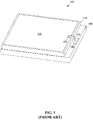
- wire bonding may be used to electrically connect electrical components on different layers of a multi-layer package 100.
- a first wire bond pad 135 provides an electrical attachment surface for a photo sensor 125 on a first die layer 110 of the multi-layer package 100.
- a second wire bond pad 195 provides an electrical attachment surface for a second die layer or substrate layer 190 of the multi-layer package 100.
- the first wire bond pad 135 and the second wire bond pad 195 are electrically connected by a bond wire 170.
- the bonding of the bond wire 170 to the first bond pad 135 generally results in portions of the bond wire "loop" 190 extending significantly above the surface of the first bond pad 135, and likewise, above the top surface of the first die layer 110.
- This protrusion of the wire loop may impede full areal access over the wafer or die 110 by optics such as lenses, filters, encapsulation epoxies and compounds, scintillator crystals, and the like.
- two or more silicon light-detection chips are placed side-by-side to form an array of light detectors.
- Examples of such light detecting arrays include medical imaging devices and astronomical telescope detectors.
- the light detecting array may include a matrix of chips, for example, a three-by-three array, or four-by four array. It may be desirable to pack the chips of this array is as closely as possible to maximize the light-detection active area relative to the mechanical dimensions of the array.
- Photo detector chips generally have a chip outline or perimeter and an active detection area within the chip outline.
- a first electrical output connection connects to a chip die on the underside of the chip and a second electrical connection connects the chip to a specific contact area of a pad on the top side of the chip.
- the chips that form an array may be individually packaged and selected after testing, for example, based on certain performance specifications.
- the individual package includes a semiconductor chip bonded onto a substrate layer. This substrate can be a sub-mount for each chip that mounts to a second plate or tile for the array. Alternatively, the chip may mount directly to the substrate which is a single tile directly holding all of the chips in the array.
- the chip is attached to its respective substrate using an electrically conductive bonding medium such as a backside contact, and a gold wire or similar bonding the chip top contact to another electrical contact area on the substrate.
- the substrate provides electrical tracking and contacts to an external device, so that each of the chips in the array can eventually be connected to suitable electronic systems nearby the detector array tile, such as amplifiers, bias voltage and voltage supplies, among others.
- the chip may then be over molded, for example, using an appropriate optically transparent epoxy compound, either individually on its sub-mount, or collectively with all the other chips on the tile, or both, once the surmounts are placed on their tile plate.
- Typical chip layouts of this type may include an active area, an edge area and the area reserved for top-side contact pad.
- the top-side contact pad is typically 100um in dimension, round, rectangular or square, with a thin bond wire ultrasonically welded to this pad.
- the other end of the wire may be bonded to the sub-mount or substrate adjacent to the pad.
- TSV Through-silicon via
- the top-side contact is made by metallization tracks deposited on the silicon to the top end of a via-type metal or conductive contact "rod” synthesized within the silicon chip from top to bottom (the TSV).
- the contact to the substrate is then made through the bottom end of the via, possibly with metal contacts, for example, bump contacts, on the chip underside.
- the via may be placed under or next to the active area of the chip and thereby takes up little or no active area surface space, and yet allows the contact to top and bottom to occur more or less within the active area of the chip.
- the TSV and bump contacts involve a complex and costly set of processes for silicon chip makers to perform and the processing of the silicon to form the vias and so forth can be detrimental to the operation of the photo-detector on the chip in any case.
- US Patent No. 7,199,345 discloses a low profile wire bond configuration for an electron sensing device in an image intensifier tube.
- the electron sensing device has a silicon die disposed on a ceramic carrier.
- the silicon die has a planar portion terminating in a step portion.
- the top surface of planar portion has an active area of the silicon die having components sensitive to light received from an electron gain device.
- a top active surface area of the silicon die has an array of bond pads that provides I/O signals to/from the silicon die.
- the array of bond pads on the top surface are electrically connected to an array of bond pads on the step by conductive stripes, extending between the top surface area, down the ramp, and onto the step.
- the silicon die is bonded to bond pads on the ceramic carrier.
- Japanese Patent Document No. JP 2007-149809 discloses a semiconductor chip with bonding pads arranged in two columns, with a bonding pad of the first column being at a first (lower) level near an outer periphery of the semiconductor chip, and a bonding pad of the second column being at a second (higher) level farther from the outer periphery of the semiconductor chip.
- JP H03-152945 discloses a hybrid integrated circuit consists of a circuit board and a semiconductor chip. A bonding pad is soldered to an electrode an upper surface of the semiconductor chip. A wire 7 extends from the bonding pad to the circuit board.
- German Patent Document No. DE 103 61 696 discloses an integrated semiconductor circuit with at least two modules or chips spatially adjacent in a common housing with an isolating element for separation.
- Embodiments of the present invention provide a reduced thickness and reduce area packaging design.
- An apparatus according to the present invention is defined in claim 1.
- a method for arranging a plurality of tiled semiconductor devices on a substrate layer according to the present invention is defined in claim 10.
- substantially means, “very nearly,” or generally within expected manufacturing tolerances.
- substantially parallel is used to mean two planes that are parallel to within an acceptable tolerance, allowing for manufacturing variations.
- a variation within one or two degrees may be considered substantially parallel for the purposes of this disclosure, as would a surface that deviates somewhat from being perfectly flat.
- electrically active region refers to a portion of a semiconductor device configured to be sensitive to electromagnetic radiation, for example, but not limited to, a photodiode or a thermopile, or a portion of a semiconductor device providing an electrical contact point to an electrical component mounted on or within the semiconductor device.
- prior art wire bond pads use planar technology, generally resulting in the bond wire loop rising significantly above the top layer of the semiconductor die or wafer being wire bonded. It is one of the objects of this invention to overcome this protrusion of the wire loop to allow full areal access over the wafer or die 110 by optics such as lenses, filters, encapsulation epoxies and compounds, scintillator crystals etc.
- optics such as lenses, filters, encapsulation epoxies and compounds, scintillator crystals etc.
- the following presents exemplary embodiments of semiconductor dies having a bond pad on a lowered section of the die so that the height of the bond wire above the die is reduced. In some preferred embodiments, the wire bond is completely below the top surface of the die.
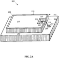
- FIGS. 2A-2B show a first example 200 of a semiconductor device that is useful for understanding the present invention.
- the bottom planar surface 260 is bonded to a second die or substrate layer 290 and may include a backside electrical connection (not shown) to the substrate layer 290.
- the wafer 210 has a height defined by the distance from the top planar surface 220 to the bottom planar surface 260.
- the wafer 210 may include an active area 225, for example, a photo sensitive region that is substantially coplanar with the top planar surface 220.
- the active area 225 may be somewhat inset within the top planar surface 220, or the active area 225 may extend somewhat above the top planar surface 220.
- the active area 225 may be surrounded by a perimeter 228 that is substantially coplanar with the top planar surface 220.
- the perimeter 228 may be formed of the material of the wafer 210, while the active area 225 is applied upon the wafer 210, or inset into the wafer 210.
- active area 225 may include a partial perimeter 225, or may not include a perimeter at all.
- a shelf 230 is formed in the wafer 210 by removing a portion of the top planar surface 220, for example, by etching a portion of the wafer 210 top planar surface 220.
- the shelf 230 may also be formed by other methods, for example, cutting or grinding away material from the wafer 210.
- the shelf 230 is substantially parallel to the top planar surface 220, and forms a surface region below the top planar surface 220 in relation to the bottom planar surface 260.
- the shelf 230 supports a device attach pad 235.
- the device attach pad 235 provides an electrical connection point to the active area 225.
- a bond wire 270 is used to form an electrical connection between the wafer 210 top side and the substrate layer 290.
- the bond wire 270 is attached to the wafer 210 via the device attach pad 235, and the bond wire 270 is attached to the substrate layer 290 via the substrate layer attach pad 295.
- the attachment between the bond wire 270 and the device attach pad 235 is made with a bond material 272 using a wire bonding technique described above, for example, ball bonding, wedge bonding, and compliant bonding.
- connection formed by the bonding material 272 of the bond wire 270 to the device attach pad 235 forms a loop in the wire 270 that raises the height of the wire 270 above the height of the shelf 230, for example, on the order of 50 to 100 ⁇ m above the surface of the shelf 230. Therefore, it is desirable to form the shelf 230 at a height sufficiently below the level of the top planar surface 220 such that the loop of wire 270 does not rise above or up to the level of the top planar surface 220, the object of this being to allow full surface contact to the active area 225 by other bodies, for example, optical lenses, filters or crystal scintillators.
- the shelf 230 includes a surface that is substantially parallel to the top planar surface 220.
- the shelf 230 includes a shelf wall 232 that may be oriented as substantially perpendicular to the shelf 230 and the top planar surface 220, as shown in FIG. 2B , or may be oriented at a non-vertical inclined angle, as shown in FIG. 2A .
- FIG. 2B As described below, other orientations of the shelf 230 and/or shelf wall 232 with respect to the top planar surface 220 are possible.
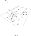
- FIG. 3A shows a second example of a semiconductor device 300 that is useful for understanding the present invention.
- the bottom planar surface 360 is bonded to a second die or substrate layer 390.
- the wafer 310 has a height defined by the distance from the top planar surface 320 to the bottom planar surface 360.
- a shelf 330 is formed in the wafer 310, for example, by etching the wafer 310. The height of the shelf 330 above the bottom planar surface 360 is less than the height of the top planar surface 320.
- the wafer 310 may include an active area 325, for example, a photo sensitive region that is substantially coplanar with the top planar surface 320.
- the active area 325 may be surrounded by a perimeter 328 that is substantially coplanar with the top planar surface 320.
- the active area 325 may be disposed somewhat above or below the top planar surface 320.
- the perimeter 328 may be formed of the material of the wafer 310, while the active area 325 is applied onto the wafer 310, or inset into the wafer 310.
- the active area 325 does not extend into the shelf 330.
- the shelf 330 supports a device attach pad 335.
- the device attach pad 335 provides an electrical connection point to the active area 325, and extends along the shelf floor 330, upward along the shelf wall 332, across a portion of the perimeter 328, and into the active region 325.
- Such a device attach pad 335 may be referred to as a bi-level attachment pad or a split level attachment pad, as it has a first level attached to the shelf 330, a portion extending upward across the shelf wall 332, and a second level extending across the perimeter 328 to the active area 325.
- the attach pad 325 is formed with a thin surface configured to lie flat against the shelf 330 and/or the top planar surface 320.
- the attach pad 325 is formed of an electrically conductive material, for example, a copper alloy, among others. At least a portion of at least one surface of the device attach pad 335 may be electrically insulated, for example, by an electrically insulating material that insulates the attach pad 335 from the shelf 330 and/or the shelf wall 332, and/or the perimeter 328.
- FIG. 3A depicts the device attach pad 335 as spanning at least a portion of the shelf 330, a shelf wall 332, and a portion of the active area 325, in order to form an electrical connection between the active area 325 and the device attach pad 335.
- the device attach pad 235 may be located entirely upon the shelf 230.
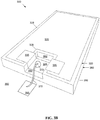
- FIG. 3B shows a variation on the second embodiment where the device attach pad 335 as spanning at least a portion of the shelf 330, a shelf wall 332, and two portions of the active area 325.
- FIG. 2B shows a shelf 230 with substantially vertical walls 232
- the second embodiment of FIG. 3A shows a shelf 330 with non-vertical walls 332
- the configuration of the shelf walls is not exclusive to these embodiments.
- a wafer 210 having an active area 235 extending into the shelf region 230 may have vertical shelf walls 232, as shown, or non-vertical shelf walls as shown in FIG. 2A .
- a wafer 310 having an active area 335 separate from the shelf region 330 may have non-vertical shelf walls 332, as shown, or vertical shelf walls, as shown in FIG. 3B .
- Other configurations are also possible.
- FIG. 3B shows a wafer 210 having an active area 235 extending into the shelf region 230
- FIG. 2A shows a wafer 310 having an active area 335 separate from the shelf region 330
- FIG. 3B shows other configurations.
- the shelf 330 may not be oriented parallel to the top planar surface 320, but instead the shelf 330 may be oriented at an incline with respect to the top planar surface 320 and the bottom planar surface 360.
- the inclined shelf 330 may include one or more walls (not shown) extending from the top planar surface to the shelf surface, as shown in FIG. 3C , or the inclined shelf surface 330 may begin to drop off directly from the top planar surface.
- the shelf 230, 330 is formed as a substantially rectangular shaped recess formed along an edge of the wafer 210, 310.
- the shelf 230, 330 may be a differently shaped recess formed along an edge of the wafer 210, 310, for example, a triangular shaped shelf, a semicircular shaped shelf, or a shelf with one or more curved walls.
- the shelf may be formed by reducing the height of the wafer 210, 310 along the entirety of one edge of the wafer 210, 310, as shown in FIG 3C .
- the shelf may be formed to include two or more edges of the wafer 210, 310.
- the pad shelf 330 has generally a relatively flat surface to facilitate attachment of the attachment pad 335.
- the pad shelf surface is in a plane parallel to the plane of the first layer, however, there is no objection to non-parallel planes, for example, a pad shelf surface 330 oriented at an incline to the plane of the top planar surface 320, as shown in FIG. 3D .
- Such a device attach pad 335 may be referred to as an angled attachment pad, as it has a first portion attached to the inclined shelf 330, and a second portion extending across the perimeter 328 to the active area 325.
- FIGS. 4 and 5A-5B show exemplary embodiments 400, 500 of a wafer 410, 510 with a shelf 430, 530 formed at a corner of the wafer 410, 510.
- the wafer 410, 510 has an active area 425, 525 in a top planar surface 420, 520 of the wafer 410, 510, and a perimeter 428, 528 surrounding the top planar surface 420, 520.
- the wafer 410, 510 has a bottom planar surface 460, 560 opposite the top planar surface 420, 520, and the shelf 430, 530 has a surface at a level between the top planar surface 420, 520 and the bottom planar surface 460, 560.
- a corner via 433, 533 is formed, for example by removing a portion of the shelf 430, 530, typically prior to bonding the wafer 410, 510 to the substrate layer 490, 590, revealing a portion of the substrate layer 490, 590 in a region that otherwise would have been covered by the wafer 410, 510 had the corner via 433, 533 not been removed.
- a substrate layer attach pad 495, 595 is attached to the substrate layer 490, 590.
- the substrate layer attach pad 495, 595 may attached to the substrate layer 490, 590 in a portion of the substrate layer 490, 590 corresponding to the corner via 433, 533 region that otherwise would have been covered by the wafer 410, 510 had the corner via 433, 533 not been removed.
- a bond wire 470, 570 is bonded to the substrate layer attach pad 495, 595 with a wire bond 472, 572 and the bond wire 470, 570 is bonded to the device attach pad 435, 535, creating an electrical connection between the wafer 410, 510 and the substrate layer 495, 595.
- the shelf 430 has two wall portions 432 that may be substantially perpendicular to one another.
- the device attach pad 435 is a split level pad, having a first level on the shelf 430 surface, a second level on the top planar surface 420 attaching to at least a portion of the active area 425 across the perimeter 428, and a connecting portion between the first level and the second level along at least one the shelf walls 432.
- the device attach pad 435 provides an electrical attachment point to the active area 425 at a location on the shelf 430, below the top planar surface 420.
- the shelf 530 has a single wall portion 532 that is formed at an angle, for example, a substantially 45° to the edges of the wafer 500.
- the shelf 530 cuts off a corner portion of the top planar surface 520.
- the device attach pad 535 is a split level pad, having a first level on the shelf 530 surface, a second level on the top planar surface 520 attaching to at least a portion of the active area 525 across the perimeter 528, and a connecting portion between the first level and the second level along the diagonal shelf wall 532.
- the device attach pad 535 provides an electrical attachment point to the active area 525 at a location on the shelf 530, below the top planar surface 520.
- FIGS. 4 and 5A-B both depict wafers 410, 510 with active areas 425, 525 that do not extend into the shelves 430, 530, there is no objection to alternative embodiments where the wafers 410, 510 have active areas 425, 525 that do extend into the shelves 430, 530.
- the device attachment pads 435, 535 may not be bi-level attachments pads, but instead be single level attachment pads confined to the shelves 430, 530, and not extending across the shelf walls 432, 532, across the perimeters 428, 528 to the active areas 425, 525.
- a wafer may be configured with a corner shelf without the corner via, so that the shelf extends to the full profile of the wafer corner, without removing a portion of the shelf to reveal a portion of the substrate layer.
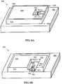
- FIG. 6A a shelf 630 is entirely inset within a top planar surface 620 of a first die 610.
- FIG. 6B shows a cutaway view of the semiconductor device 600 having an inset shelf 630.
- the inset shelf 630 is surrounded by a shelf wall 632.
- a through via 633 is formed though the surface of the shelf 630 to an attachment pad 695 on the surface of a second die 690, accessible by the through via 633.
- An active area 625 of the wafer 610 extends through the shelf 630, and a device attach pad 635 is located within the shelf 630.
- a bond wire 670 is attached to the device attachment pad 635 with a wire bond 672, as described above regarding the first embodiment.
- the bond wire 670 provides an electrical connection between the substrate attach pad 695 and the device attach pad 635.
- the active area 625 does not extend to the shelf 630, and a split level attach pad (not shown) is used to form an electrical attachment between the active area 625 and the shelf 630.
- An over mold encapsulant may be applied over the shelf and/or active layer in any of the abovementioned embodiments.
- the encapsulation may be formed of a transparent material applied as a resin, such as epoxy, which thereafter hardens to form a protective coating over the shelf and entire wafer 210, 310, 410, 510, 610.
- the encapsulant may be applied to all of the shelf, a portion of the shelf, or over all or a portion of the top planar surface. It is preferable that the encapsulant be applied to entirely cover any bond wire 270, 370, 470, 570, 670 attached to the device attach pad 235, 335, 435, 535, 635.
- the shelf and the device attachment pad on the shelf may be relocated to allow reduced die length, width or area, allowing for smaller package length, width, or area.
- the overall chip size may be reduced for the same active area in comparison to the arrangement of the prior art attachment pad where the wire bond pad has to be moved well away from the active area so that an object can be attached directly to the active area.
- Advantages of the above embodiments may include thinner packages, for example, surface mount photodiode for smart phone applications where the die needs a protective overcoat. Since this coat is preferably thick enough to encapsulate the wire bond, if the bond is lowered the thickness of the encapsulant may be consequently lowered, thereby reducing overall package thickness.
- Such configurations may, for example, allow an X-ray responsive (scintillator) crystal to be attached directly to a light sensitive die for better coupling of the light from the crystal to the photodiode die.
- such configurations may also allow optical filters to be attached directly to a light sensitive die for reduced overall height and reduced light leakage that occurs from light entering the gap between the filter and the die.
- These configurations may allow the die to be reduced in length, width or area without significantly compromising the sensitivity of the die to light. Therefore such object/die single entities may be mounted closer side by side for higher packing density and improved detection efficiency and/or reduced array packaging area, as described further below.
- the shelf may be formed either before or after the photosensitive region is applied to the upper die. It may be advantageous to form the shelf before forming the photosensitive region, as a thin photosensitive region may then be applied, in comparison to forming a thicker photosensitive region which is then etched to form the pad shelf region.
- the height of the shelf is advantageously low enough below the top surface such that a loop of wire extending upward from a wire attach pad on the shelf is level with or below the height of the top surface. Accordingly, the difference in height between the shelf and the top surface is preferably on the order of at least 50-100 ⁇ m. Similarly, it is desirable that the thickness of the shelf is thin enough to accommodate the appropriate drop in elevation below the top surface, yet thick enough for mechanical stability, for example, on the order of at least 100-200 ⁇ m.
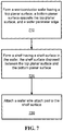
- a method for forming a semiconductor device is shown by the flowchart of FIG. 7 .
- any process descriptions or blocks in flowcharts should be understood as representing modules, segments, portions of code, or steps that include one or more instructions for implementing specific logical functions in the process, and in alternative implementations functions may be executed out of order from that shown or discussed, including substantially concurrently or in reverse order, depending on the functionality involved, as would be understood by those reasonably skilled in the art of the present invention.
- a semiconductor wafer having a top planar surface, a bottom planar surface opposite the top planar surface, and a wafer perimeter edge is formed, as shown by block 710.
- a shelf having a shelf surface is formed in the wafer, the shelf surface disposed between the top planar surface and the bottom planar surface, as shown by block 720.
- a wafer wire attach pad is attached to the shelf surface, as shown by block 730.
- some of the abovementioned embodiments may be used to achieve higher packing density for array of chips.
- some of the abovementioned embodiments provide a device and method for a chip having the chip corner cut off or otherwise removed in a corner area of the chip to minimize the area needed for wire bonding on the substrate layer, so that the area for the package may be significantly reduced.
- the chip active area may extend as close to the chip edge as possible on all four sides of the chip, with the exception of the small edge or corner shelf area.
- FIG. 8 shows an exemplary embodiment of an arrangement of four tiled semiconductor devices 500A-D with corner vias according to the fourth embodiment described above.
- the semiconductor devices 500A-D are arranged so that each has a corner via is co-located in a common via region 810, depicted with a dashed line.
- Each of the four semiconductor devices 500A-D has a corner via positioned in a different corner.
- the common via region 810 exposes the substrate layer 590.
- Four substrate layer attach pads 595 are attached to the substrate layer 590 within the common via region 810, such that the active region 525 ( FIG. 5A ) of each semiconductor device may be individually attached to a corresponding substrate layer attach pad 595.
- the electrical attachment of the active region 525 FIG.
- FIG. 5A may be formed by a device attach pad 535 ( FIG. 5A ) attached to a shelf 530 ( FIG. 5A ), using a bond wire (not shown), as described above.
- two or more of the semiconductor devices 500A-D may be attached to a common substrate layer attach pad 595 in the common via region 810.
- embodiments may incorporate non-rectangular semiconductor devices, such that the non-rectangular semiconductor devices are arranged on a substrate layer such that five, six, or more corner vias converge within a common via region 810.
- FIG. 8 shows four semiconductor devices 500A-D with corner vias in the common via region 810, in alternative embodiments the common via region 810 may accommodate the corner vias of two or three semiconductor devices 500A-D.
- Examples of semiconductor packages that may benefit from reduced area and/or reduced thickness include, but are not limited to arrays of sensors for imaging applications such as x-ray inspection systems, high energy physics experiments, Positron Emission Tomography medical systems, and consumer electronics where reducing thickness of components is critical to reducing overall thickness of the electronic devices.
- FIG. 9A is a schematic diagram of an exemplary eighth embodiment of a semiconductor device 900.
- a first die or wafer 910 formed of a semiconductor material has a top planar surface 920 and a bottom planar surface 960 substantially parallel to the top planar surface 920.
- the bottom planar surface 960 is bonded to a second die or substrate layer 990 and may include a backside electrical connection (not shown) to the substrate layer 990.
- the wafer 910 may include an active area 925 that is substantially coplanar with the top planar surface 920, may be somewhat inset beneath the top planar surface 920, or may protrude somewhat above the top planar surface 920.
- the active area 925 is optionally surrounded by a perimeter 928 that is substantially coplanar with the top planar surface 920.
- a first shelf 930 is a corner shelf formed in the wafer 910 by removing a corner portion of the top planar surface 920, for example, by etching a portion of the wafer 910 top planar surface 920.
- the first shelf 930 supports a first device attach pad 935.
- the first device attach pad 935 provides an electrical connection point to the active area 925.
- a first bond wire 970a may be used to form an electrical connection between the active area 925 and the substrate layer 990.
- the first bond wire 970a is attached to the wafer 910 at the first device attach pad 935.
- the first bond wire 970a is attached to the substrate layer 990 at a first substrate layer attach pad 995a, located on a portion of the substrate layer 990 exposed by a corner via 933.
- the attachment between the first bond wire 970a and the first device attach pad 935 is made with a bond material 972.
- a second shelf 940 is an edge shelf formed in the wafer 910 by removing an edge portion of the top planar surface 920.
- the second shelf 940 supports a second device attach pad 945.
- the second device attach pad 945 provides a second electrical connection point, for example, to the active area 925, or to another portion of the wafer 910, or to another component (not shown) mounted on the wafer 910.
- the second device attach pad 945 may be used in lieu of a backside attach point.
- a photodiode active region 925 may have both an anode contact and a cathode contact located on top of the wafer 910.
- a wafer 910 with an array of junctions may include contacts for each junction on one, two, or more shelves.
- a second bond wire 970b may be attached to the wafer 910 at the second device attach pad 945, forming an electrical connection to the second substrate layer attach pad 995b.
- the second bond wire 970b is attached to the substrate layer 990 at the second substrate layer attach pad 995b, located on a portion of the substrate layer 990 exposed by an edge via 943.
- the attachment between the second bond wire 970b and the second device attach pad 945 may made with a bond material (not shown).
- FIG. 9B is a schematic diagram of a variation of the exemplary eighth embodiment of a semiconductor device. This variation is substantially similar to the eighth embodiment, except the second shelf 940 includes an edge via 943.
- the edge via 943 removes a portion of the wafer 910 below the second shelf 940, so that when the wafer 910 is bonded to the substrate layer 990, a portion of the substrate layer 990 is revealed in the location where the edge via 943 was removed.
- the second bond wire 970b is not shown in FIG. 9B .
- FIG. 10 is a schematic diagram of an exemplary ninth embodiment of a semiconductor device.
- the ninth embodiment is substantially similar to the variation of the eighth embodiment shown in FIG. 9B , with the addition of a second active area.
- a first die or wafer 1010 formed of a semiconductor material has a top planar surface 1020 and a bottom planar surface 1060 substantially parallel to the top planar surface 1020.
- the bottom planar surface 1060 is bonded to a second die or substrate layer 1090 and may include a backside electrical connection (not shown) to the substrate layer 1090.
- the top planar surface 1020 of a wafer 1010 may include two or more active areas 1025a, 1025b, and each active area 1025a, 1025 may have an independent shelf 1030, 1040.
- the active areas 1025a, 1025b are surrounded by a perimeter 1028 that is substantially coplanar with the top planar surface 1020.
- a first shelf 1030 is a corner shelf formed in the wafer 1010 by removing a corner portion of the top planar surface 1020, for example, by etching a portion of the wafer 1010 top planar surface 1020.
- the first shelf 1030 supports a first device attach pad 1035.
- the first device attach pad 1035 may provide an electrical connection point to the first active area 1025a.
- a first bond wire 1070a is used to form an electrical connection between the wafer 1010, for example, the first active area 1025a, and the substrate layer 990.
- the first bond wire 1070a is attached to the wafer 1010 at the first device attach pad 1035.
- the first bond wire 1070a is attached to the substrate layer 1090 at a first substrate layer attach pad 1095a, located on a portion of the substrate layer 1090 exposed by a corner via 1033.
- the attachment between the first bond wire 1070a and the first device attach pad 1035 may be made with a bond material 1072.
- a second shelf 1040 is an edge shelf formed in the wafer 1010 by removing an edge portion of the top planar surface 1020.
- the second shelf 1040 supports a second device attach pad 1045.
- the second device attach pad 1045 provides a second electrical connection point, for example, to the second active area 1025b, or to another portion of the wafer 1010, or to another component (not shown) mounted on the wafer 1010.
- the second device attach pad 1045 may be used in lieu of a backside attach point.
- a second bond wire 1070b may be attached to the wafer 1010 at the second device attach pad 1045, forming an electrical connection to the second substrate layer attach pad 1095b.
- the second bond wire 1070b is attached to the substrate layer 1090 at the second substrate layer attach pad 1095b, located on a portion of the substrate layer 990 exposed by an edge via 943.
- the attachment between the second bond wire 970b and the second device attach pad 945 may made with a bond material 1072.
Landscapes
- Solid State Image Pick-Up Elements (AREA)
- Wire Bonding (AREA)
- Internal Circuitry In Semiconductor Integrated Circuit Devices (AREA)
Claims (15)
- Vorrichtung mit:einer Substratschicht (290) mit einer Fläche, die ein Substratschicht-Drahtbefestigungspad (295) aufweist; undeiner Vielzahl von wie Kacheln angeordneten Halbleitervorrichtungen (200), die auf der Substratschichtfläche montiert sind, wobei jede Halbleitervorrichtung aufweist:eine obere planare Fläche (220, 320, 420, 520, 620, 920, 1020), die ferner einen elektrisch aktiven Bereich (225) aufweist;eine untere planare Fläche (260, 360, 460, 560, 660, 960, 1060), die im Wesentlichen parallel zu der oberen planaren Fläche angeordnet ist und von der oberen planaren Fläche durch die Vorrichtungshöhe getrennt ist;einen Fachbereich (230), der zwischen der oberen planaren Fläche und der unteren planare Fläche angeordnet ist, wobei der Fachbereich eine Fachfläche mit einer Fachhöhe aufweist, die geringer als die Vorrichtungshöhe ist;eine Kantenaussparung, die durch Entfernen eines Abschnitts des Fachbereichs gebildet wird; undein Vorrichtungs-Drahtbefestigungspad (235, 335, 435, 535, 635, 935, 945, 1035, 1045), das in elektrischer Kommunikation mit dem aktiven Bereich ist;wobei das Vorrichtungs-Drahtbefestigungspad zumindest teilweise auf dem Fachbereich angeordnet ist;wobei die untere planare Fläche benachbart zu der Substratschicht angeordnet ist, wobei die untere planare Fläche einen Abschnitt der Substratschichtfläche bedeckt, mit Ausnahme des Substratschicht-Drahtbefestigungspads (295, 395, 495, 595, 695, 995a, 995b, 1095a, 1095b),dadurch gekennzeichnet, dassdie Kantenaussparung einer ersten der Halbleitervorrichtungen benachbart zu der Kantenaussparung einer zweiten der Halbleitervorrichtungen ist, undeine elektrische Verbindung zwischen dem Vorrichtungs-Drahtbefestigungspad und dem Substratschicht-Drahtbefestigungspad vorgesehen ist.
- Vorrichtung nach Anspruch 1, wobei die Fachfläche im Wesentlichen parallel zu der oberen planaren Fläche ist.
- Vorrichtung nach Anspruch 2, ferner mit einer Fachwand, die sich zwischen der Fachfläche und der oberen planaren Fläche entlang mindestens einem Abstand des Fachbereichs erstreckt, wobei die Fachwand im Wesentlichen senkrecht zu der oberen planaren Fläche der Fachfläche ist.
- Vorrichtung nach Anspruch 1, wobei die obere planare Fläche ferner einen Umfang aufweist, der den aktiven Bereich zumindest teilweise umgibt, wobei der Fachbereich zumindest teilweise innerhalb des Umfangsbereichs ausgebildet ist.
- Vorrichtung nach Anspruch 4, wobei sich das Vorrichtungs-Drahtbefestigungspad zwischen mindestens einem Abschnitt der oberen planaren Fläche und mindestens einem Abschnitt des Fachbereichs erstreckt.
- Vorrichtung nach Anspruch 1, wobei die obere planare Fläche ferner einen Umfang aufweist, der den aktiven Bereich zumindest teilweise umgibt, wobei sich der aktive Bereich sowohl über die obere planare Fläche als auch über den Fachbereich erstreckt.
- Vorrichtung nach Anspruch 1, wobei das Substratschicht-Drahtbefestigungspad durch Entfernen eines Abschnitts des Fachs freigelegt ist, wobei das Fach im Wesentlichen in einer Ecke der oberen planaren Fläche angeordnet ist.
- Vorrichtung nach Anspruch 7, wobei der Abschnitt des Fachs, der zum Freilegen des Substratschicht-Drahtbefestigungspads entfernt ist, eine Aussparung durch die Vorrichtung aufweist.
- Vorrichtung nach Anspruch 1, ferner mit einer optisch transparenten Umspritzung, die zum Einfassen des Fachs und des Vorrichtungs-Drahtbefestigungspads angeordnet ist.
- Verfahren zum Positionieren einer Vielzahl von wie Kacheln angeordneten Halbleitervorrichtungen (200) auf einer Substratschicht (290), mit folgenden Schritten:
Bilden der Vielzahl von wie Kacheln angeordneten Halbleitervorrichtungen durch:Bilden eines im Wesentlichen rechteckigen Halbleiterwafers, der eine obere planare Fläche (220, 320, 420, 520, 620, 920, 1020), eine untere planare Fläche (260, 360, 460, 560, 660, 960, 1060) gegenüber der oberen planaren Fläche und eine Wafer-Umfangskante aufweist;Bilden eines Fachs (230), das eine Fachfläche in dem Wafer aufweist, wobei die Fachfläche in einer Kante des rechteckigen Wafers zwischen der oberen planaren Fläche und der unteren planaren Fläche angeordnet ist;Entfernen eines Abschnitts des Fachs zum Bilden einer Kantenaussparung;undAnbringen eines Vorrichtungs-Drahtbefestigungspads (235, 335, 435, 535, 635, 935, 945, 1035, 1045) an der Fachfläche;Anbringen einer ersten der Vielzahl von wie Kacheln angeordneten Halbleitervorrichtungen an der Substratschicht; undAnbringen einer zweiten der Vielzahl von wie Kacheln angeordneten Halbleitervorrichtungen an der Substratschicht, wobei die Kantenaussparung der ersten Halbleitervorrichtung benachbart zu der Kantenaussparung der zweiten Halbleitervorrichtung ist. - Verfahren nach Anspruch 10, ferner mit folgenden Schritten:Bilden eines ersten Substratschicht-Drahtbefestigungspads auf der Substratschichtfläche in einem Abschnitt der Substratschicht, der von der Kantenaussparung der ersten Vorrichtung offengelegt wird;elektrisches Verbinden des ersten Vorrichtungs-Drahtbefestigungspads mit dem ersten Substratschicht-Drahtbefestigungspad.
- Verfahren nach Anspruch 10, wobei die Fachfläche ein Eckfach aufweist, das in einer Ecke des rechteckigen Wafers angeordnet ist; und
die Kantenaussparung eine Eckenaussparung aufweist, die in einer Ecke der Fachfläche ausgebildet ist. - Verfahren nach Anspruch 10, wobei die Kantenaussparung der ersten Vorrichtung eine Eckenaussparung ist und wobei die Kantenaussparung der zweiten Vorrichtung eine Eckenaussparung ist.
- Verfahren nach Anspruch 10, ferner umfassend:Anbringen einer dritten der Vielzahl von Halbleitervorrichtungen an der Substratschicht; undAnbringen einer vierten der Vielzahl von Halbleitervorrichtungen an der Substratschicht,wobei die Kantenaussparung der ersten bis vierten Vorrichtung der Vielzahl von Halbleitervorrichtungen eine Eckenaussparung ist und wobei sich die Eckenaussparung der ersten Vorrichtung, die Eckenaussparung der zweiten Vorrichtung, die Eckenaussparung der dritten Vorrichtung und die Eckenaussparung der vierten Vorrichtung in einem gemeinsamen Aussparungsbereich befinden.
- Verfahren nach Anspruch 14, wobei der gemeinsame Aussparungsbereich die Substratschicht freilegt, wobei das Verfahren ferner umfasst:
Anbringen von vier Substratschicht-Befestigungspads an der Substratschicht innerhalb des gemeinsamen Aussparungsbereichs, so dass ein aktiver Bereich für jede Halbleitervorrichtung einzeln mit einem entsprechenden Substratschicht-Befestigungspad elektrisch verbunden ist.
Applications Claiming Priority (1)
| Application Number | Priority Date | Filing Date | Title |
|---|---|---|---|
| US14/220,167 US9117721B1 (en) | 2014-03-20 | 2014-03-20 | Reduced thickness and reduced footprint semiconductor packaging |
Publications (3)
| Publication Number | Publication Date |
|---|---|
| EP2924728A2 EP2924728A2 (de) | 2015-09-30 |
| EP2924728A3 EP2924728A3 (de) | 2016-07-20 |
| EP2924728B1 true EP2924728B1 (de) | 2020-05-27 |
Family
ID=52784928
Family Applications (1)
| Application Number | Title | Priority Date | Filing Date |
|---|---|---|---|
| EP15160048.3A Not-in-force EP2924728B1 (de) | 2014-03-20 | 2015-03-20 | Bondfläche für eine Halbleiteranordnung und entsprechendes Verfahren |
Country Status (4)
| Country | Link |
|---|---|
| US (1) | US9117721B1 (de) |
| EP (1) | EP2924728B1 (de) |
| JP (1) | JP2015185846A (de) |
| CN (1) | CN104934403A (de) |
Cited By (1)
| Publication number | Priority date | Publication date | Assignee | Title |
|---|---|---|---|---|
| EP3273478B1 (de) * | 2015-03-18 | 2025-04-30 | Hamamatsu Photonics K.K. | Lichtdetektionsvorrichtung |
Families Citing this family (8)
| Publication number | Priority date | Publication date | Assignee | Title |
|---|---|---|---|---|
| JP6004441B2 (ja) * | 2013-11-29 | 2016-10-05 | インターナショナル・ビジネス・マシーンズ・コーポレーションInternational Business Machines Corporation | 基板接合方法、バンプ形成方法及び半導体装置 |
| JP6381477B2 (ja) * | 2015-04-13 | 2018-08-29 | 浜松ホトニクス株式会社 | 光検出装置 |
| US9588240B1 (en) * | 2015-10-27 | 2017-03-07 | General Electric Company | Digital readout architecture for four side buttable digital X-ray detector |
| US10283557B2 (en) | 2015-12-31 | 2019-05-07 | General Electric Company | Radiation detector assembly |
| US10686003B2 (en) | 2015-12-31 | 2020-06-16 | General Electric Company | Radiation detector assembly |
| KR102027522B1 (ko) * | 2017-04-13 | 2019-10-01 | (주)파트론 | 광학센서 패키지 및 그 제조 방법 |
| WO2020208850A1 (ja) * | 2019-04-09 | 2020-10-15 | 株式会社カイジョー | 絶縁被覆線の接合方法、接続構造、絶縁被覆線の剥離方法及びボンディング装置 |
| FR3112423A1 (fr) * | 2020-07-09 | 2022-01-14 | Trixell | Procédé de réalisation d’un imageur |
Family Cites Families (14)
| Publication number | Priority date | Publication date | Assignee | Title |
|---|---|---|---|---|
| US4622574A (en) * | 1985-07-29 | 1986-11-11 | The Perkin-Elmer Corporation | Semiconductor chip with recessed bond pads |
| US4845405A (en) * | 1986-05-14 | 1989-07-04 | Sanyo Electric Co., Ltd. | Monolithic LED display |
| JPH02177340A (ja) * | 1988-12-27 | 1990-07-10 | Mitsubishi Electric Corp | 半導体装置 |
| JPH03152945A (ja) * | 1989-11-09 | 1991-06-28 | Fuji Electric Co Ltd | 半導体チップのワイヤボンディング方法 |
| FR2788882A1 (fr) * | 1999-01-27 | 2000-07-28 | Schlumberger Systems & Service | Dispositif a circuits integres, module electronique pour carte a puce utilisant le dispositif et procede de fabrication dudit dispositif |
| US20030230796A1 (en) * | 2002-06-12 | 2003-12-18 | Aminuddin Ismail | Stacked die semiconductor device |
| US7261230B2 (en) * | 2003-08-29 | 2007-08-28 | Freescale Semiconductor, Inc. | Wirebonding insulated wire and capillary therefor |
| DE10361696B4 (de) * | 2003-12-30 | 2016-03-10 | Infineon Technologies Ag | Verfahren zum Herstellen einer integrierten Halbleiterschaltungsanordnung |
| US7199345B1 (en) * | 2004-03-26 | 2007-04-03 | Itt Manufacturing Enterprises Inc. | Low profile wire bond for an electron sensing device in an image intensifier tube |
| JP2007134486A (ja) * | 2005-11-10 | 2007-05-31 | Toshiba Corp | 積層型半導体装置及びその製造方法 |
| JP2007149809A (ja) * | 2005-11-25 | 2007-06-14 | Renesas Technology Corp | 半導体装置およびその製造方法 |
| JP5481769B2 (ja) * | 2006-11-22 | 2014-04-23 | 日亜化学工業株式会社 | 半導体装置及びその製造方法 |
| GB2451447B (en) | 2007-07-30 | 2012-01-11 | Sensl Technologies Ltd | Light sensor |
| CN101615587A (zh) * | 2008-06-27 | 2009-12-30 | 桑迪士克股份有限公司 | 半导体装置中的导线层叠式缝线接合 |
-
2014
- 2014-03-20 US US14/220,167 patent/US9117721B1/en active Active
-
2015
- 2015-02-27 JP JP2015037895A patent/JP2015185846A/ja active Pending
- 2015-03-20 EP EP15160048.3A patent/EP2924728B1/de not_active Not-in-force
- 2015-03-20 CN CN201510125526.7A patent/CN104934403A/zh active Pending
Non-Patent Citations (1)
| Title |
|---|
| None * |
Cited By (1)
| Publication number | Priority date | Publication date | Assignee | Title |
|---|---|---|---|---|
| EP3273478B1 (de) * | 2015-03-18 | 2025-04-30 | Hamamatsu Photonics K.K. | Lichtdetektionsvorrichtung |
Also Published As
| Publication number | Publication date |
|---|---|
| EP2924728A3 (de) | 2016-07-20 |
| EP2924728A2 (de) | 2015-09-30 |
| CN104934403A (zh) | 2015-09-23 |
| US9117721B1 (en) | 2015-08-25 |
| JP2015185846A (ja) | 2015-10-22 |
Similar Documents
| Publication | Publication Date | Title |
|---|---|---|
| US9117721B1 (en) | Reduced thickness and reduced footprint semiconductor packaging | |
| US8092734B2 (en) | Covers for microelectronic imagers and methods for wafer-level packaging of microelectronics imagers | |
| CN101675516B (zh) | 具有通过过孔连接到前侧触头的后侧触头的芯片 | |
| US20090039527A1 (en) | Sensor-type package and method for fabricating the same | |
| EP1492168B1 (de) | Sensor | |
| KR101524359B1 (ko) | 로우 프로파일 이미지 센서 패키지 및 방법 | |
| US7301214B2 (en) | Component of a radiation detector comprising a substrate with positioning structure for a photoelectric element array | |
| KR100651105B1 (ko) | 광반도체 장치 및 그 제조 방법 | |
| US7646075B2 (en) | Microelectronic imagers having front side contacts | |
| EP1554760B1 (de) | Schaltungssubstrat und verfahren | |
| US20040197954A1 (en) | Chip scale image sensor semiconductor package and method of fabrication | |
| US20060138626A1 (en) | Microelectronic packages using a ceramic substrate having a window and a conductive surface region | |
| US20080265443A1 (en) | Semiconductor device and method of manufacturing the same | |
| TWI525756B (zh) | 有受控模造邊界的層壓無引線載體組件中的光半導體元件及形成該元件之方法 | |
| KR20150033584A (ko) | 쿨링 피처를 갖는 저프로파일 센서 패키지와 이를 제조하는 방법 | |
| US9276030B2 (en) | Read out integrated circuit input/output routing on permanent carrier | |
| KR200489765Y1 (ko) | 센서 모듈 | |
| EP2950345A1 (de) | Großflächiges Bildsensormodul und Verfahren zur Herstellung eines großflächigen Bildsensors | |
| US6988899B2 (en) | Electronic assembly, and apparatus and method for the assembly thereof | |
| US9000344B2 (en) | Focal plane array periphery through-vias for read out integrated circuit | |
| US7612442B2 (en) | Semiconductor device | |
| US20260026119A1 (en) | Semiconductor package having a stepped molding structure | |
| US20140035080A1 (en) | Wafer Level Camera Module Structure | |
| CN108389912A (zh) | 一种非制冷红外探测器芯片及其封装结构和制备方法 |
Legal Events
| Date | Code | Title | Description |
|---|---|---|---|
| PUAI | Public reference made under article 153(3) epc to a published international application that has entered the european phase |
Free format text: ORIGINAL CODE: 0009012 |
|
| AK | Designated contracting states |
Kind code of ref document: A2 Designated state(s): AL AT BE BG CH CY CZ DE DK EE ES FI FR GB GR HR HU IE IS IT LI LT LU LV MC MK MT NL NO PL PT RO RS SE SI SK SM TR |
|
| AX | Request for extension of the european patent |
Extension state: BA ME |
|
| RIC1 | Information provided on ipc code assigned before grant |
Ipc: H01L 27/146 20060101ALN20151106BHEP Ipc: H01L 23/485 20060101AFI20151106BHEP Ipc: H01L 29/06 20060101ALI20151106BHEP Ipc: H01L 23/49 20060101ALI20151106BHEP |
|
| PUAL | Search report despatched |
Free format text: ORIGINAL CODE: 0009013 |
|
| AK | Designated contracting states |
Kind code of ref document: A3 Designated state(s): AL AT BE BG CH CY CZ DE DK EE ES FI FR GB GR HR HU IE IS IT LI LT LU LV MC MK MT NL NO PL PT RO RS SE SI SK SM TR |
|
| AX | Request for extension of the european patent |
Extension state: BA ME |
|
| RIC1 | Information provided on ipc code assigned before grant |
Ipc: H01L 23/49 20060101ALI20160613BHEP Ipc: H01L 23/485 20060101AFI20160613BHEP Ipc: H01L 27/146 20060101ALN20160613BHEP Ipc: H01L 29/06 20060101ALI20160613BHEP |
|
| STAA | Information on the status of an ep patent application or granted ep patent |
Free format text: STATUS: THE APPLICATION HAS BEEN PUBLISHED |
|
| STAA | Information on the status of an ep patent application or granted ep patent |
Free format text: STATUS: REQUEST FOR EXAMINATION WAS MADE |
|
| 17P | Request for examination filed |
Effective date: 20170123 |
|
| RBV | Designated contracting states (corrected) |
Designated state(s): AL AT BE BG CH CY CZ DE DK EE ES FI FR GB GR HR HU IE IS IT LI LT LU LV MC MK MT NL NO PL PT RO RS SE SI SK SM TR |
|
| RIC1 | Information provided on ipc code assigned before grant |
Ipc: H01L 23/485 20060101ALI20190930BHEP Ipc: H01L 23/00 20060101AFI20190930BHEP Ipc: H01L 23/49 20060101ALI20190930BHEP Ipc: H01L 27/146 20060101ALN20190930BHEP Ipc: H01L 29/06 20060101ALI20190930BHEP |
|
| GRAP | Despatch of communication of intention to grant a patent |
Free format text: ORIGINAL CODE: EPIDOSNIGR1 |
|
| STAA | Information on the status of an ep patent application or granted ep patent |
Free format text: STATUS: GRANT OF PATENT IS INTENDED |
|
| RIC1 | Information provided on ipc code assigned before grant |
Ipc: H01L 23/485 20060101ALI20191010BHEP Ipc: H01L 23/00 20060101AFI20191010BHEP Ipc: H01L 27/146 20060101ALN20191010BHEP Ipc: H01L 23/49 20060101ALI20191010BHEP |
|
| INTG | Intention to grant announced |
Effective date: 20191113 |
|
| RIC1 | Information provided on ipc code assigned before grant |
Ipc: H01L 23/49 20060101ALI20191105BHEP Ipc: H01L 23/485 20060101ALI20191105BHEP Ipc: H01L 23/00 20060101AFI20191105BHEP Ipc: H01L 27/146 20060101ALN20191105BHEP |
|
| GRAS | Grant fee paid |
Free format text: ORIGINAL CODE: EPIDOSNIGR3 |
|
| GRAJ | Information related to disapproval of communication of intention to grant by the applicant or resumption of examination proceedings by the epo deleted |
Free format text: ORIGINAL CODE: EPIDOSDIGR1 |
|
| GRAL | Information related to payment of fee for publishing/printing deleted |
Free format text: ORIGINAL CODE: EPIDOSDIGR3 |
|
| STAA | Information on the status of an ep patent application or granted ep patent |
Free format text: STATUS: REQUEST FOR EXAMINATION WAS MADE |
|
| REG | Reference to a national code |
Ref country code: DE Ref legal event code: R079 Ref document number: 602015053236 Country of ref document: DE Free format text: PREVIOUS MAIN CLASS: H01L0023485000 Ipc: H01L0023000000 |
|
| INTC | Intention to grant announced (deleted) | ||
| GRAR | Information related to intention to grant a patent recorded |
Free format text: ORIGINAL CODE: EPIDOSNIGR71 |
|
| STAA | Information on the status of an ep patent application or granted ep patent |
Free format text: STATUS: GRANT OF PATENT IS INTENDED |
|
| RIC1 | Information provided on ipc code assigned before grant |
Ipc: H01L 27/146 20060101ALN20200319BHEP Ipc: H01L 23/485 20060101ALI20200319BHEP Ipc: H01L 23/49 20060101ALI20200319BHEP Ipc: H01L 23/00 20060101AFI20200319BHEP |
|
| GRAA | (expected) grant |
Free format text: ORIGINAL CODE: 0009210 |
|
| STAA | Information on the status of an ep patent application or granted ep patent |
Free format text: STATUS: THE PATENT HAS BEEN GRANTED |
|
| AK | Designated contracting states |
Kind code of ref document: B1 Designated state(s): AL AT BE BG CH CY CZ DE DK EE ES FI FR GB GR HR HU IE IS IT LI LT LU LV MC MK MT NL NO PL PT RO RS SE SI SK SM TR |
|
| INTG | Intention to grant announced |
Effective date: 20200417 |
|
| REG | Reference to a national code |
Ref country code: GB Ref legal event code: FG4D |
|
| REG | Reference to a national code |
Ref country code: CH Ref legal event code: EP |
|
| REG | Reference to a national code |
Ref country code: AT Ref legal event code: REF Ref document number: 1275452 Country of ref document: AT Kind code of ref document: T Effective date: 20200615 |
|
| REG | Reference to a national code |
Ref country code: DE Ref legal event code: R096 Ref document number: 602015053236 Country of ref document: DE |
|
| REG | Reference to a national code |
Ref country code: LT Ref legal event code: MG4D |
|
| PG25 | Lapsed in a contracting state [announced via postgrant information from national office to epo] |
Ref country code: GR Free format text: LAPSE BECAUSE OF FAILURE TO SUBMIT A TRANSLATION OF THE DESCRIPTION OR TO PAY THE FEE WITHIN THE PRESCRIBED TIME-LIMIT Effective date: 20200828 Ref country code: FI Free format text: LAPSE BECAUSE OF FAILURE TO SUBMIT A TRANSLATION OF THE DESCRIPTION OR TO PAY THE FEE WITHIN THE PRESCRIBED TIME-LIMIT Effective date: 20200527 Ref country code: NO Free format text: LAPSE BECAUSE OF FAILURE TO SUBMIT A TRANSLATION OF THE DESCRIPTION OR TO PAY THE FEE WITHIN THE PRESCRIBED TIME-LIMIT Effective date: 20200827 Ref country code: IS Free format text: LAPSE BECAUSE OF FAILURE TO SUBMIT A TRANSLATION OF THE DESCRIPTION OR TO PAY THE FEE WITHIN THE PRESCRIBED TIME-LIMIT Effective date: 20200927 Ref country code: LT Free format text: LAPSE BECAUSE OF FAILURE TO SUBMIT A TRANSLATION OF THE DESCRIPTION OR TO PAY THE FEE WITHIN THE PRESCRIBED TIME-LIMIT Effective date: 20200527 Ref country code: SE Free format text: LAPSE BECAUSE OF FAILURE TO SUBMIT A TRANSLATION OF THE DESCRIPTION OR TO PAY THE FEE WITHIN THE PRESCRIBED TIME-LIMIT Effective date: 20200527 Ref country code: PT Free format text: LAPSE BECAUSE OF FAILURE TO SUBMIT A TRANSLATION OF THE DESCRIPTION OR TO PAY THE FEE WITHIN THE PRESCRIBED TIME-LIMIT Effective date: 20200928 |
|
| REG | Reference to a national code |
Ref country code: NL Ref legal event code: MP Effective date: 20200527 |
|
| PG25 | Lapsed in a contracting state [announced via postgrant information from national office to epo] |
Ref country code: HR Free format text: LAPSE BECAUSE OF FAILURE TO SUBMIT A TRANSLATION OF THE DESCRIPTION OR TO PAY THE FEE WITHIN THE PRESCRIBED TIME-LIMIT Effective date: 20200527 Ref country code: LV Free format text: LAPSE BECAUSE OF FAILURE TO SUBMIT A TRANSLATION OF THE DESCRIPTION OR TO PAY THE FEE WITHIN THE PRESCRIBED TIME-LIMIT Effective date: 20200527 Ref country code: RS Free format text: LAPSE BECAUSE OF FAILURE TO SUBMIT A TRANSLATION OF THE DESCRIPTION OR TO PAY THE FEE WITHIN THE PRESCRIBED TIME-LIMIT Effective date: 20200527 Ref country code: BG Free format text: LAPSE BECAUSE OF FAILURE TO SUBMIT A TRANSLATION OF THE DESCRIPTION OR TO PAY THE FEE WITHIN THE PRESCRIBED TIME-LIMIT Effective date: 20200827 |
|
| REG | Reference to a national code |
Ref country code: AT Ref legal event code: MK05 Ref document number: 1275452 Country of ref document: AT Kind code of ref document: T Effective date: 20200527 |
|
| PG25 | Lapsed in a contracting state [announced via postgrant information from national office to epo] |
Ref country code: AL Free format text: LAPSE BECAUSE OF FAILURE TO SUBMIT A TRANSLATION OF THE DESCRIPTION OR TO PAY THE FEE WITHIN THE PRESCRIBED TIME-LIMIT Effective date: 20200527 Ref country code: NL Free format text: LAPSE BECAUSE OF FAILURE TO SUBMIT A TRANSLATION OF THE DESCRIPTION OR TO PAY THE FEE WITHIN THE PRESCRIBED TIME-LIMIT Effective date: 20200527 |
|
| PG25 | Lapsed in a contracting state [announced via postgrant information from national office to epo] |
Ref country code: ES Free format text: LAPSE BECAUSE OF FAILURE TO SUBMIT A TRANSLATION OF THE DESCRIPTION OR TO PAY THE FEE WITHIN THE PRESCRIBED TIME-LIMIT Effective date: 20200527 Ref country code: CZ Free format text: LAPSE BECAUSE OF FAILURE TO SUBMIT A TRANSLATION OF THE DESCRIPTION OR TO PAY THE FEE WITHIN THE PRESCRIBED TIME-LIMIT Effective date: 20200527 Ref country code: RO Free format text: LAPSE BECAUSE OF FAILURE TO SUBMIT A TRANSLATION OF THE DESCRIPTION OR TO PAY THE FEE WITHIN THE PRESCRIBED TIME-LIMIT Effective date: 20200527 Ref country code: EE Free format text: LAPSE BECAUSE OF FAILURE TO SUBMIT A TRANSLATION OF THE DESCRIPTION OR TO PAY THE FEE WITHIN THE PRESCRIBED TIME-LIMIT Effective date: 20200527 Ref country code: DK Free format text: LAPSE BECAUSE OF FAILURE TO SUBMIT A TRANSLATION OF THE DESCRIPTION OR TO PAY THE FEE WITHIN THE PRESCRIBED TIME-LIMIT Effective date: 20200527 Ref country code: AT Free format text: LAPSE BECAUSE OF FAILURE TO SUBMIT A TRANSLATION OF THE DESCRIPTION OR TO PAY THE FEE WITHIN THE PRESCRIBED TIME-LIMIT Effective date: 20200527 Ref country code: IT Free format text: LAPSE BECAUSE OF FAILURE TO SUBMIT A TRANSLATION OF THE DESCRIPTION OR TO PAY THE FEE WITHIN THE PRESCRIBED TIME-LIMIT Effective date: 20200527 Ref country code: SM Free format text: LAPSE BECAUSE OF FAILURE TO SUBMIT A TRANSLATION OF THE DESCRIPTION OR TO PAY THE FEE WITHIN THE PRESCRIBED TIME-LIMIT Effective date: 20200527 |
|
| PG25 | Lapsed in a contracting state [announced via postgrant information from national office to epo] |
Ref country code: PL Free format text: LAPSE BECAUSE OF FAILURE TO SUBMIT A TRANSLATION OF THE DESCRIPTION OR TO PAY THE FEE WITHIN THE PRESCRIBED TIME-LIMIT Effective date: 20200527 Ref country code: SK Free format text: LAPSE BECAUSE OF FAILURE TO SUBMIT A TRANSLATION OF THE DESCRIPTION OR TO PAY THE FEE WITHIN THE PRESCRIBED TIME-LIMIT Effective date: 20200527 |
|
| REG | Reference to a national code |
Ref country code: DE Ref legal event code: R097 Ref document number: 602015053236 Country of ref document: DE |
|
| PLBE | No opposition filed within time limit |
Free format text: ORIGINAL CODE: 0009261 |
|
| STAA | Information on the status of an ep patent application or granted ep patent |
Free format text: STATUS: NO OPPOSITION FILED WITHIN TIME LIMIT |
|
| 26N | No opposition filed |
Effective date: 20210302 |
|
| PG25 | Lapsed in a contracting state [announced via postgrant information from national office to epo] |
Ref country code: SI Free format text: LAPSE BECAUSE OF FAILURE TO SUBMIT A TRANSLATION OF THE DESCRIPTION OR TO PAY THE FEE WITHIN THE PRESCRIBED TIME-LIMIT Effective date: 20200527 |
|
| PG25 | Lapsed in a contracting state [announced via postgrant information from national office to epo] |
Ref country code: MC Free format text: LAPSE BECAUSE OF FAILURE TO SUBMIT A TRANSLATION OF THE DESCRIPTION OR TO PAY THE FEE WITHIN THE PRESCRIBED TIME-LIMIT Effective date: 20200527 |
|
| REG | Reference to a national code |
Ref country code: CH Ref legal event code: PL |
|
| GBPC | Gb: european patent ceased through non-payment of renewal fee |
Effective date: 20210320 |
|
| REG | Reference to a national code |
Ref country code: BE Ref legal event code: MM Effective date: 20210331 |
|
| PG25 | Lapsed in a contracting state [announced via postgrant information from national office to epo] |
Ref country code: LU Free format text: LAPSE BECAUSE OF NON-PAYMENT OF DUE FEES Effective date: 20210320 Ref country code: LI Free format text: LAPSE BECAUSE OF NON-PAYMENT OF DUE FEES Effective date: 20210331 Ref country code: CH Free format text: LAPSE BECAUSE OF NON-PAYMENT OF DUE FEES Effective date: 20210331 Ref country code: FR Free format text: LAPSE BECAUSE OF NON-PAYMENT OF DUE FEES Effective date: 20210331 Ref country code: IE Free format text: LAPSE BECAUSE OF NON-PAYMENT OF DUE FEES Effective date: 20210320 Ref country code: GB Free format text: LAPSE BECAUSE OF NON-PAYMENT OF DUE FEES Effective date: 20210320 |
|
| PG25 | Lapsed in a contracting state [announced via postgrant information from national office to epo] |
Ref country code: BE Free format text: LAPSE BECAUSE OF NON-PAYMENT OF DUE FEES Effective date: 20210331 |
|
| PG25 | Lapsed in a contracting state [announced via postgrant information from national office to epo] |
Ref country code: HU Free format text: LAPSE BECAUSE OF FAILURE TO SUBMIT A TRANSLATION OF THE DESCRIPTION OR TO PAY THE FEE WITHIN THE PRESCRIBED TIME-LIMIT; INVALID AB INITIO Effective date: 20150320 |
|
| P01 | Opt-out of the competence of the unified patent court (upc) registered |
Effective date: 20230521 |
|
| PG25 | Lapsed in a contracting state [announced via postgrant information from national office to epo] |
Ref country code: CY Free format text: LAPSE BECAUSE OF FAILURE TO SUBMIT A TRANSLATION OF THE DESCRIPTION OR TO PAY THE FEE WITHIN THE PRESCRIBED TIME-LIMIT Effective date: 20200527 |
|
| PG25 | Lapsed in a contracting state [announced via postgrant information from national office to epo] |
Ref country code: MK Free format text: LAPSE BECAUSE OF FAILURE TO SUBMIT A TRANSLATION OF THE DESCRIPTION OR TO PAY THE FEE WITHIN THE PRESCRIBED TIME-LIMIT Effective date: 20200527 |
|
| PGFP | Annual fee paid to national office [announced via postgrant information from national office to epo] |
Ref country code: DE Payment date: 20240327 Year of fee payment: 10 |
|
| PG25 | Lapsed in a contracting state [announced via postgrant information from national office to epo] |
Ref country code: MT Free format text: LAPSE BECAUSE OF FAILURE TO SUBMIT A TRANSLATION OF THE DESCRIPTION OR TO PAY THE FEE WITHIN THE PRESCRIBED TIME-LIMIT Effective date: 20200527 |
|
| REG | Reference to a national code |
Ref country code: DE Ref legal event code: R119 Ref document number: 602015053236 Country of ref document: DE |
|
| PG25 | Lapsed in a contracting state [announced via postgrant information from national office to epo] |
Ref country code: TR Free format text: LAPSE BECAUSE OF FAILURE TO SUBMIT A TRANSLATION OF THE DESCRIPTION OR TO PAY THE FEE WITHIN THE PRESCRIBED TIME-LIMIT Effective date: 20200527 |
|
| PG25 | Lapsed in a contracting state [announced via postgrant information from national office to epo] |
Ref country code: DE Free format text: LAPSE BECAUSE OF NON-PAYMENT OF DUE FEES Effective date: 20251001 |