EP2922707B1 - Capacitive micro-machined transducer and method of manufacturing the same - Google Patents
Capacitive micro-machined transducer and method of manufacturing the same Download PDFInfo
- Publication number
- EP2922707B1 EP2922707B1 EP13792500.4A EP13792500A EP2922707B1 EP 2922707 B1 EP2922707 B1 EP 2922707B1 EP 13792500 A EP13792500 A EP 13792500A EP 2922707 B1 EP2922707 B1 EP 2922707B1
- Authority
- EP
- European Patent Office
- Prior art keywords
- layer
- dielectric
- electrode layer
- layers
- cavity
- Prior art date
- Legal status (The legal status is an assumption and is not a legal conclusion. Google has not performed a legal analysis and makes no representation as to the accuracy of the status listed.)
- Active
Links
- 238000004519 manufacturing process Methods 0.000 title claims description 17
- 238000000034 method Methods 0.000 claims description 96
- 238000000231 atomic layer deposition Methods 0.000 claims description 82
- 238000000059 patterning Methods 0.000 claims description 74
- 238000005530 etching Methods 0.000 claims description 46
- 239000000758 substrate Substances 0.000 claims description 43
- 238000000151 deposition Methods 0.000 claims description 39
- 239000000463 material Substances 0.000 claims description 28
- 239000004020 conductor Substances 0.000 claims description 23
- 229910052755 nonmetal Inorganic materials 0.000 claims description 12
- HTXDPTMKBJXEOW-UHFFFAOYSA-N iridium(IV) oxide Inorganic materials O=[Ir]=O HTXDPTMKBJXEOW-UHFFFAOYSA-N 0.000 claims description 5
- ITWBWJFEJCHKSN-UHFFFAOYSA-N 1,4,7-triazonane Chemical compound C1CNCCNCCN1 ITWBWJFEJCHKSN-UHFFFAOYSA-N 0.000 claims description 3
- 229910002340 LaNiO3 Inorganic materials 0.000 claims description 3
- 229910002353 SrRuO3 Inorganic materials 0.000 claims description 3
- ATJFFYVFTNAWJD-UHFFFAOYSA-N Tin Chemical compound [Sn] ATJFFYVFTNAWJD-UHFFFAOYSA-N 0.000 claims 2
- -1 ITO Inorganic materials 0.000 claims 1
- 239000010410 layer Substances 0.000 description 461
- 239000010408 film Substances 0.000 description 96
- PNEYBMLMFCGWSK-UHFFFAOYSA-N Alumina Chemical compound [O-2].[O-2].[O-2].[Al+3].[Al+3] PNEYBMLMFCGWSK-UHFFFAOYSA-N 0.000 description 68
- 238000002955 isolation Methods 0.000 description 21
- 238000002604 ultrasonography Methods 0.000 description 16
- 239000002346 layers by function Substances 0.000 description 15
- NRTOMJZYCJJWKI-UHFFFAOYSA-N Titanium nitride Chemical compound [Ti]#N NRTOMJZYCJJWKI-UHFFFAOYSA-N 0.000 description 11
- 239000012528 membrane Substances 0.000 description 11
- 238000012545 processing Methods 0.000 description 11
- 230000008021 deposition Effects 0.000 description 9
- 238000001004 secondary ion mass spectrometry Methods 0.000 description 9
- 229910000449 hafnium oxide Inorganic materials 0.000 description 8
- 229910052751 metal Inorganic materials 0.000 description 8
- 239000002184 metal Substances 0.000 description 8
- 238000004833 X-ray photoelectron spectroscopy Methods 0.000 description 6
- WIHZLLGSGQNAGK-UHFFFAOYSA-N hafnium(4+);oxygen(2-) Chemical compound [O-2].[O-2].[Hf+4] WIHZLLGSGQNAGK-UHFFFAOYSA-N 0.000 description 6
- PXHVJJICTQNCMI-UHFFFAOYSA-N nickel Substances [Ni] PXHVJJICTQNCMI-UHFFFAOYSA-N 0.000 description 6
- 238000000623 plasma-assisted chemical vapour deposition Methods 0.000 description 6
- BASFCYQUMIYNBI-UHFFFAOYSA-N platinum Substances [Pt] BASFCYQUMIYNBI-UHFFFAOYSA-N 0.000 description 6
- 230000015556 catabolic process Effects 0.000 description 5
- 239000003989 dielectric material Substances 0.000 description 5
- 150000004767 nitrides Chemical class 0.000 description 5
- TWNQGVIAIRXVLR-UHFFFAOYSA-N oxo(oxoalumanyloxy)alumane Chemical compound O=[Al]O[Al]=O TWNQGVIAIRXVLR-UHFFFAOYSA-N 0.000 description 5
- 239000010949 copper Substances 0.000 description 4
- 229910052759 nickel Inorganic materials 0.000 description 4
- 239000002243 precursor Substances 0.000 description 4
- MZLGASXMSKOWSE-UHFFFAOYSA-N tantalum nitride Chemical compound [Ta]#N MZLGASXMSKOWSE-UHFFFAOYSA-N 0.000 description 4
- 101100163897 Caenorhabditis elegans asic-2 gene Proteins 0.000 description 3
- 101100269850 Caenorhabditis elegans mask-1 gene Proteins 0.000 description 3
- OKTJSMMVPCPJKN-UHFFFAOYSA-N Carbon Chemical compound [C] OKTJSMMVPCPJKN-UHFFFAOYSA-N 0.000 description 3
- 239000004411 aluminium Substances 0.000 description 3
- 229910052782 aluminium Inorganic materials 0.000 description 3
- XAGFODPZIPBFFR-UHFFFAOYSA-N aluminium Chemical compound [Al] XAGFODPZIPBFFR-UHFFFAOYSA-N 0.000 description 3
- 230000009286 beneficial effect Effects 0.000 description 3
- 229910052799 carbon Inorganic materials 0.000 description 3
- 230000001419 dependent effect Effects 0.000 description 3
- CJNBYAVZURUTKZ-UHFFFAOYSA-N hafnium(iv) oxide Chemical compound O=[Hf]=O CJNBYAVZURUTKZ-UHFFFAOYSA-N 0.000 description 3
- 238000003384 imaging method Methods 0.000 description 3
- 230000035945 sensitivity Effects 0.000 description 3
- 229910052710 silicon Inorganic materials 0.000 description 3
- 239000010703 silicon Substances 0.000 description 3
- XKRFYHLGVUSROY-UHFFFAOYSA-N Argon Chemical compound [Ar] XKRFYHLGVUSROY-UHFFFAOYSA-N 0.000 description 2
- ZAMOUSCENKQFHK-UHFFFAOYSA-N Chlorine atom Chemical compound [Cl] ZAMOUSCENKQFHK-UHFFFAOYSA-N 0.000 description 2
- RYGMFSIKBFXOCR-UHFFFAOYSA-N Copper Chemical compound [Cu] RYGMFSIKBFXOCR-UHFFFAOYSA-N 0.000 description 2
- 229910045601 alloy Inorganic materials 0.000 description 2
- 239000000956 alloy Substances 0.000 description 2
- 229940024548 aluminum oxide Drugs 0.000 description 2
- 238000003491 array Methods 0.000 description 2
- 238000012512 characterization method Methods 0.000 description 2
- 238000006243 chemical reaction Methods 0.000 description 2
- 229910052801 chlorine Inorganic materials 0.000 description 2
- 239000000460 chlorine Substances 0.000 description 2
- 229910052802 copper Inorganic materials 0.000 description 2
- 238000011161 development Methods 0.000 description 2
- 238000010586 diagram Methods 0.000 description 2
- 230000005684 electric field Effects 0.000 description 2
- 238000010292 electrical insulation Methods 0.000 description 2
- AMGQUBHHOARCQH-UHFFFAOYSA-N indium;oxotin Chemical compound [In].[Sn]=O AMGQUBHHOARCQH-UHFFFAOYSA-N 0.000 description 2
- 229910052741 iridium Inorganic materials 0.000 description 2
- GKOZUEZYRPOHIO-UHFFFAOYSA-N iridium atom Chemical compound [Ir] GKOZUEZYRPOHIO-UHFFFAOYSA-N 0.000 description 2
- 229910000457 iridium oxide Inorganic materials 0.000 description 2
- 239000000203 mixture Substances 0.000 description 2
- 229910052697 platinum Inorganic materials 0.000 description 2
- 229920001296 polysiloxane Polymers 0.000 description 2
- 239000004065 semiconductor Substances 0.000 description 2
- LIVNPJMFVYWSIS-UHFFFAOYSA-N silicon monoxide Chemical compound [Si-]#[O+] LIVNPJMFVYWSIS-UHFFFAOYSA-N 0.000 description 2
- 238000004544 sputter deposition Methods 0.000 description 2
- 229910052712 strontium Inorganic materials 0.000 description 2
- CIOAGBVUUVVLOB-UHFFFAOYSA-N strontium atom Chemical compound [Sr] CIOAGBVUUVVLOB-UHFFFAOYSA-N 0.000 description 2
- 239000000126 substance Substances 0.000 description 2
- 239000010409 thin film Substances 0.000 description 2
- WFKWXMTUELFFGS-UHFFFAOYSA-N tungsten Chemical compound [W] WFKWXMTUELFFGS-UHFFFAOYSA-N 0.000 description 2
- 229910052721 tungsten Inorganic materials 0.000 description 2
- 239000010937 tungsten Substances 0.000 description 2
- 229910052581 Si3N4 Inorganic materials 0.000 description 1
- VYPSYNLAJGMNEJ-UHFFFAOYSA-N Silicium dioxide Chemical compound O=[Si]=O VYPSYNLAJGMNEJ-UHFFFAOYSA-N 0.000 description 1
- 229910052786 argon Inorganic materials 0.000 description 1
- 239000003990 capacitor Substances 0.000 description 1
- 238000001311 chemical methods and process Methods 0.000 description 1
- 238000004140 cleaning Methods 0.000 description 1
- 239000013078 crystal Substances 0.000 description 1
- OWJUDUZMAXZIOA-UHFFFAOYSA-N dialuminum hafnium(4+) oxygen(2-) Chemical compound [O--].[O--].[O--].[Al+3].[Al+3].[Hf+4] OWJUDUZMAXZIOA-UHFFFAOYSA-N 0.000 description 1
- 229910003460 diamond Inorganic materials 0.000 description 1
- 239000010432 diamond Substances 0.000 description 1
- 230000000694 effects Effects 0.000 description 1
- 239000007789 gas Substances 0.000 description 1
- 238000001459 lithography Methods 0.000 description 1
- 239000011159 matrix material Substances 0.000 description 1
- 238000005259 measurement Methods 0.000 description 1
- 238000012986 modification Methods 0.000 description 1
- 230000004048 modification Effects 0.000 description 1
- 229910021420 polycrystalline silicon Inorganic materials 0.000 description 1
- 229920005591 polysilicon Polymers 0.000 description 1
- HQVNEWCFYHHQES-UHFFFAOYSA-N silicon nitride Chemical compound N12[Si]34N5[Si]62N3[Si]51N64 HQVNEWCFYHHQES-UHFFFAOYSA-N 0.000 description 1
- 229910052814 silicon oxide Inorganic materials 0.000 description 1
- 238000004088 simulation Methods 0.000 description 1
- 238000007736 thin film deposition technique Methods 0.000 description 1
Images


Classifications
-
- G—PHYSICS
- G10—MUSICAL INSTRUMENTS; ACOUSTICS
- G10K—SOUND-PRODUCING DEVICES; METHODS OR DEVICES FOR PROTECTING AGAINST, OR FOR DAMPING, NOISE OR OTHER ACOUSTIC WAVES IN GENERAL; ACOUSTICS NOT OTHERWISE PROVIDED FOR
- G10K11/00—Methods or devices for transmitting, conducting or directing sound in general; Methods or devices for protecting against, or for damping, noise or other acoustic waves in general
- G10K11/18—Methods or devices for transmitting, conducting or directing sound
-
- B—PERFORMING OPERATIONS; TRANSPORTING
- B06—GENERATING OR TRANSMITTING MECHANICAL VIBRATIONS IN GENERAL
- B06B—METHODS OR APPARATUS FOR GENERATING OR TRANSMITTING MECHANICAL VIBRATIONS OF INFRASONIC, SONIC, OR ULTRASONIC FREQUENCY, e.g. FOR PERFORMING MECHANICAL WORK IN GENERAL
- B06B1/00—Methods or apparatus for generating mechanical vibrations of infrasonic, sonic, or ultrasonic frequency
- B06B1/02—Methods or apparatus for generating mechanical vibrations of infrasonic, sonic, or ultrasonic frequency making use of electrical energy
- B06B1/0292—Electrostatic transducers, e.g. electret-type
-
- C—CHEMISTRY; METALLURGY
- C23—COATING METALLIC MATERIAL; COATING MATERIAL WITH METALLIC MATERIAL; CHEMICAL SURFACE TREATMENT; DIFFUSION TREATMENT OF METALLIC MATERIAL; COATING BY VACUUM EVAPORATION, BY SPUTTERING, BY ION IMPLANTATION OR BY CHEMICAL VAPOUR DEPOSITION, IN GENERAL; INHIBITING CORROSION OF METALLIC MATERIAL OR INCRUSTATION IN GENERAL
- C23C—COATING METALLIC MATERIAL; COATING MATERIAL WITH METALLIC MATERIAL; SURFACE TREATMENT OF METALLIC MATERIAL BY DIFFUSION INTO THE SURFACE, BY CHEMICAL CONVERSION OR SUBSTITUTION; COATING BY VACUUM EVAPORATION, BY SPUTTERING, BY ION IMPLANTATION OR BY CHEMICAL VAPOUR DEPOSITION, IN GENERAL
- C23C16/00—Chemical coating by decomposition of gaseous compounds, without leaving reaction products of surface material in the coating, i.e. chemical vapour deposition [CVD] processes
- C23C16/44—Chemical coating by decomposition of gaseous compounds, without leaving reaction products of surface material in the coating, i.e. chemical vapour deposition [CVD] processes characterised by the method of coating
- C23C16/455—Chemical coating by decomposition of gaseous compounds, without leaving reaction products of surface material in the coating, i.e. chemical vapour deposition [CVD] processes characterised by the method of coating characterised by the method used for introducing gases into reaction chamber or for modifying gas flows in reaction chamber
- C23C16/45523—Pulsed gas flow or change of composition over time
- C23C16/45525—Atomic layer deposition [ALD]
-
- C—CHEMISTRY; METALLURGY
- C23—COATING METALLIC MATERIAL; COATING MATERIAL WITH METALLIC MATERIAL; CHEMICAL SURFACE TREATMENT; DIFFUSION TREATMENT OF METALLIC MATERIAL; COATING BY VACUUM EVAPORATION, BY SPUTTERING, BY ION IMPLANTATION OR BY CHEMICAL VAPOUR DEPOSITION, IN GENERAL; INHIBITING CORROSION OF METALLIC MATERIAL OR INCRUSTATION IN GENERAL
- C23C—COATING METALLIC MATERIAL; COATING MATERIAL WITH METALLIC MATERIAL; SURFACE TREATMENT OF METALLIC MATERIAL BY DIFFUSION INTO THE SURFACE, BY CHEMICAL CONVERSION OR SUBSTITUTION; COATING BY VACUUM EVAPORATION, BY SPUTTERING, BY ION IMPLANTATION OR BY CHEMICAL VAPOUR DEPOSITION, IN GENERAL
- C23C16/00—Chemical coating by decomposition of gaseous compounds, without leaving reaction products of surface material in the coating, i.e. chemical vapour deposition [CVD] processes
- C23C16/56—After-treatment
Definitions
- the present invention relates to a method of manufacturing a capacitive micro-machined transducer, in particular a capacitive micro-machined ultrasound transducer (CMUT) for transmitting and/or receiving ultrasound waves.
- the present invention further relates to a capacitive micro-machined transducer, in particular a capacitive micro-machined ultrasound transducer (CMUT) for transmitting and/or receiving ultrasound.
- CMUT capacitive micro-machined ultrasound transducer
- CMUT capacitive micro-machined ultrasound transducers
- ultrasound waves For receiving ultrasound waves, ultrasound waves cause the membrane to move or vibrate and the variation in capacitance between the electrodes can be detected. Thereby, the ultrasound waves are transformed into a corresponding electrical signal. Conversely, an electrical signal applied to the electrodes causes the membrane to move or vibrate and thereby transmitting ultrasound waves.
- WO 2010/032156 A2 describes a capacitive micro-machined ultrasound transducer with a specific layer structure which solves the charging problem.
- a first isolation layer comprising a dielectric is arranged between the first electrode and the second electrode.
- a second isolation layer comprising a dielectric can be arranged between the second electrode and the cavity.
- ONO Oxide-Nitride-Oxide
- the first dielectric isolation layer and the second dielectric isolation layer electrically isolate the first electrode and the second electrode.
- Such dielectric isolation layers determine to a fair extent the overall performance of the CMUT device. In the ideal case, dielectric isolation layers are very thin or have high dielectric constant and a high breakdown voltage.
- an ONO dielectric layer has its limitations and can be deposited only at relative thick layers (e.g. about 250 nm using "Plasma-enhanced chemical vapor deposition" (PECVD)) and a low dielectric constant, as the dielectric constant of nitride is about 5 to 7.
- the performance of the CMUT is limited by a minimum thickness of the ONO dielectric layer, the electrical breakdown voltage and its dielectric constant.
- a particular problem with such a CMUT device can be that the operating voltage is rather high and the output pressure relatively low. Therefore, there is a need to further improve such a CMUT.
- a method of manufacturing a capacitive micro-machined transducer according to claim 1, in particular a CMUT comprising: depositing a sacrificial layer, the sacrificial layer being removable for forming a cavity of the transducer, removing the sacrificial layer by providing an etch hole and etching the sacrificial layer for forming a cavity, and wherein subsequently at least one of the following steps is performed: depositing a first electrode layer and a second electrode layer in the cavity by Atomic Layer Deposition, and/or depositing a first dielectric film on the first electrode layer and a second dielectric film on the second electrode layer in the cavity by Atomic Layer Deposition, wherein the deposited first and second dielectric films cover the top surface and the bottom surface as well as the side surfaces of the cavity.
- a capacitive micro-machined transducer manufactured by the method of the present invention.
- the transducer comprises a capacitive micro-machined transducer, in particular a CMUT, is presented, comprising: a first electrode layer on a substrate, a first dielectric film on the first electrode layer, a cavity formed above the first dielectric film, a second dielectric film covering the cavity, and a second electrode layer on the second dielectric film, wherein both the first and second dielectric films cover a top surface and a bottom surface as well as the side surface of the cavity.
- ALD Atomic Layer Deposition
- the ALD technique provides advantages and options to overcome the current processing limitations and, accordingly, the CMUT performance limitations.
- a manufacturing method is provided in which all CMUT functional layers are deposited in one single process sequence, in particular under a controlled environment without exposing the substrate to the ambient environment as would be necessary during prior art processing in general.
- the CMUT functional layers are in particular the first electrode layer (providing the first electrode), the first dielectric film (providing electrical insulation), the sacrificial layer (forming the cavity), the second dielectric film (providing electrical insulation), and the second electrode film (providing the second electrode).
- This process is also called the All Layer ALD (AL-ALD) CMUT process.
- This invention relates to improving the performance of CMUT devices significantly.
- One essential processing step in realizing CMUT devices forms the opening of the cavity by etching the sacrificial layer. This step still influences device performance significantly.
- the invention proposes to first realize the cavity by etching the sacrificial layers and subsequently growing the dielectric films and/or the metal layers (electrode layers) by ALD through the already existing openings. By this, it is possible to clean the cavity perfectly. Subsequently, the dielectric films and/or the electrode layers are added which, due to their subsequent application, do not suffer from any chemical attack after deposition.
- a step of cleaning the cavity from etching residues is performed after the step of etching the sacrificial layer and prior to the deposition of the first and second electrode layers and/or the first and second dielectric films in the cavity by ALD.
- the manufacturing method partly uses in particular "top-to-bottom" patterning.
- the top-to-bottom patterning provides a CMUT with a characteristic pyramid structure, in particular step pyramid structure.
- This typical cross section can be identified via analyzing methods using, for example, a FIB or SEM (Scanning Electron Microscope) cross section.
- Patterning means bringing the structure (e.g. stack of deposited layers) into a pattern. This can for example be performed using (photo) lithography where a photo sensitive is exposed. The exposure tool is called a Stepper. A photo sensitive layer, called a Resist, is developed. The pattern can be etched into a layer. The etching process can be a "wet" or "dry” process.
- Atomic Layer Deposition is a thin film deposition technique that is based on the sequential use of a gas phase chemical process.
- the majority of ALD reactions use two chemicals, typically called "precursors". These precursors react with a surface one-at-a-time in a sequential manner.
- ALD is a self-limiting (i.e. the amount of the thin material deposited in each reaction cycle is constant), sequential surface chemistry that deposits conformal thin-films of materials onto substrates of varying compositions.
- ALD deposited layers generally are amorphous.
- ALD deposited layers generally have a high quality, are pinhole free and can be deposited at low temperatures. Due to the low process temperature ALD is CMOS compatible.
- a thinner dielectric isolation layer results in more output pressure at a lower operating voltage and improved receive sensitivity. This is because the membrane is attracted by an electrical force between the electrodes in a direction towards the bottom of the cavity.
- a thin dielectric film or a material having a high dielectric constant also called high-epsilon material or high-k material
- the first dielectric film and/or the second dielectric film comprises a first layer comprising an oxide, a second layer comprising a high-k material, and a third layer comprising an oxide.
- the dielectric isolation layer comprises an oxide layer (O), a high-k layer, and another oxide layer (O).
- a high-k layer is sandwiched between two oxide layers (in particular silicone oxide). This is a so-called laminate.
- High-k refers to a high dielectric constant (e.g. 8 or more).
- the dielectric constant is commonly abbreviated by the letter k (or also ⁇ r ).
- the transducer performance can be significantly improved (e.g.
- the high-k material is Aluminium Oxide (Al 2 O 3 ) and/or Hafnium Oxide (HfO 2 ). Aluminium Oxide (k or ⁇ r between 7 and 9, in particular about 8 or 9) or Hafnium Oxide (k or ⁇ r between 12 and 27, in particular about 14 or 20) has a high dielectric constant.
- a laminate (alternating layers) of Oxide - Aluminium Oxide - Oxide (abbreviated by OAO) can be provided in this way.
- a laminate (alternating layers) of Oxide - Hafnium Oxide - Oxide (abbreviated by OHO) can be provided in this way.
- the second layer comprises a first sublayer comprising Aluminium Oxide, a second sublayer comprising Hafnium Oxide, and a third sublayer comprising Aluminium Oxide.
- a laminate (alternating layers) of Oxide - Aluminium Oxide - Hafnium Oxide - Aluminium Oxide - Oxide (abbreviated by OAHAO) can be provided.
- Aluminium Oxide also referred to as Alumina
- Hafnium Oxide has an even higher dielectric constant but a low breakdown voltage. Therefore, an OAHAO dielectric isolation layer combines low stress, a high dielectric constant and a high breakdown voltage.
- the second layer has a thickness below 100nm. In this way a very thin high-k layer can be provided, in particular using ALD.
- At least one of deposited layers is patterned prior to the step of removing the sacrificial layer.
- at least one of the CMUT functional layers deposited prior to etching is patterned.
- the first electrode layer, the sacrificial layer and/or the second electrode layer may be patterned.
- This patterning can comprise multiple steps, for example a first step of patterning the top most layer(s) and a second step of patterning the bottom most layer(s).
- the layers can be patterned to have a different lateral dimension (in a direction parallel to the top surface(s) of the layers). In this way, a (step) pyramid structure can be created.
- patterning can be performed in a single step in which the layers are patterned to have the same lateral dimension.
- patterning comprises the steps of depositing the second electrode layer on the sacrificial layer by Atomic Layer Deposition (ALD) prior to the step of removing the sacrificial layer, and patterning the second electrode layer.
- ALD Atomic Layer Deposition
- the lateral dimension of the second electrode can be defined.
- the second electrode layer can be patterned to be smaller than the first electrode layer.
- “top-to-bottom” patterning may be performed (e.g. using a first etching mask).
- a characteristic pyramid structure, in particular step pyramid structure is thus provided.
- the method comprises the steps of depositing the first electrode layer on a substrate by Atomic Layer Deposition prior to the step of removing the sacrificial layer, and patterning the first electrode layer.
- the method comprises the steps of depositing the sacrificial layer by Atomic Layer Deposition, and patterning the sacrificial layer. By patterning the sacrificial layer, the lateral dimension of the cavity can be defined. The "top-to-bottom" patterning may be further performed (e.g. using a second etching mask) in this way.
- the patterning of the sacrificial layer can be performed in a step separate from the step of patterning the second electrode layer.
- the patterning of the sacrificial layer and the patterning of the second electrode layer can be performed in a common step.
- the lateral dimension of the first electrode can be defined.
- the "top-to-bottom" patterning may be further performed (e.g. using a third etching mask) in this way.
- the patterning of the first electrode layer can be performed in a step separate from the step of patterning the second electrode layer and/or the step of patterning the sacrificial layer.
- the patterning of the first electrode layer and the patterning of the sacrificial layer can be performed in a common step. This can also be performed in a common step with patterning of the second electrode layer.
- most of or all the deposited layers and films are patterned.
- most of or all of the layers and films deposited by ALD are patterned after the ALD deposition.
- all of the CMUT functional layers are patterned.
- This patterning can comprise multiple steps, for example a first step of patterning the top most layer(s) and a second step of patterning the bottom most layer(s).
- the layers can be patterned to have a different lateral dimension (in a direction parallel to the top surface(s) of the layers). In this way, a (step) pyramid structure can be created.
- patterning can be performed in a single step in which the layers are patterned to have the same lateral dimension.
- the method further comprises depositing a dielectric layer covering the deposited layers.
- This depositing step can in particular be performed using Atomic Layer Deposition.
- the dielectric layer can in particular cover top surfaces and side surfaces of the deposited layers and films with essentially the same coverage. This provides a very good step coverage, in particular by Atomic Layer Deposition.
- the method further comprises removing the sacrificial layer by providing an etch hole and etching the sacrificial layer for forming the cavity.
- the cavity of the CMUT is provided (e.g. using a fourth etching mask) in an easy manner.
- the first electrode layer and/or the second electrode layer comprises a non-metal conductive material.
- the non-metal conductive material can for example be a semiconductor.
- the non-metal conductive material is at least one material selected from the group comprising TiN (Titanium Nitride), TaN (Tantalum Nitride), TaCN, IrO 2 (Iridium Oxide), ITO (Indium Tin Oxide), LaNiO 3 , and SrRuO 3 (Strontium Ruthenate). These materials are suitable for Atomic Layer Deposition.
- the non-metal conductive material is TiN (Titanium Nitride). Titanium Nitride is particularly suitable, in particular for Atomic Layer Deposition. For example, Titanium Nitride has a low electrical resistance (e.g. compared to polysilicone) and/or can be deposited as a very thin layer (e.g. compared to polysilicone).
- the first and second electrode layers extend adjacently to the first and second dielectric films, respectively, around the cavity.
- the first and second electrode layers are deposited via ALD in the cavity subsequently to etching the sacrificial layer.
- the first and second electrode layers are deposited in the cavity by ALD.
- the first and second dielectric films are deposited in the cavity by ALD.
- the cavity is surrounded by the dielectric films.
- the first and second electrode layers are positioned adjacent to the dielectric films.
- the first electrode layer and/or the second electrode layer comprises a metal conductive material.
- the metal conductive material can comprise at least one material selected from the group comprising Ni (Nickel), Copper (Cu), W (Tungsten), Pt (Platinum), Ir (Iridium), and Al (Aluminium).
- the metal can be an alloy thereof.
- the first dielectric film and/or the second dielectric film comprises process residuals, such as Carbon or Chlorine residuals. These residuals may be remainders of the pre-cursor(s) used in the ALD process. This shows that the CMUT has been manufactured using Atomic Layer Deposition.
- the residuals can for example be detected using XPS (X-ray photoelectron spectroscopy) or other characterization methods, such as SIMS (Secondary Ion Mass spectroscopy).
- the at least one patterned layer and/or film ends abruptly or non-continuously at its sides.
- the top surface and the side surface of a layer are substantially orthogonal to each other.
- the CMUT has been manufactured using patterning.
- the top surface and the side surface of a layer are orthogonal (90°) or at a right angle to each other.
- the layer has some slope due to the patterning (in particular etching) process not being perfect, or deliberately a slope may be applied.
- the etching rates of the various materials are not equal.
- the top surface and the side surface of the layer at its end will no be a perfect right angle.
- substantially orthogonal can be understood to be an angle between 70° and 110° (90° ⁇ 20°), or between 80° and 100° (90° ⁇ 10°), or between 85° and 95° (90° ⁇ 5°).
- the second electrode layer is patterned to be smaller than the first electrode layer. This shows that the CMUT has been manufactured using "top-to-bottom” patterning. A characteristic pyramid structure, in particular step pyramid structure, is thus provided.
- the CMUT further comprises at least one conductive via extending from the first electrode layer and/or the second electrode layer in a direction orthogonal to the top surfaces of the layers.
- the conductive via is orthogonal or at a right angle to the deposited layers.
- the first electrode, the second electrode, or both can be provided with an electrical connection.
- the conductive via may be electrically connected to an ASIC underneath the CMUT.
- the CMUT further comprises a dielectric layer covering the deposited layers and films.
- the dielectric layer covers top surfaces and side surfaces of the deposited layers and films with essentially the same coverage. This shows that the CMUT provides a very good step coverage, in particular using Atomic Layer Deposition.
- vertical portions of the dielectric layer can extend substantially orthogonal to the deposited layers and/or films. As explained above, substantially orthogonal can be understood to be an angle between 70° and 110° (90° ⁇ 20°), or between 80° and 100° (90° ⁇ 10°), or between 85° and 95° (90° ⁇ 5°).
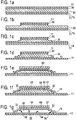
- Fig. 1a-k show a method of manufacturing a CMUT 100 according to a first embodiment.
- Fig. 1b-j show a schematic top to bottom process flow, after all functional CMUT layers have been deposited in one process sequence (see Fig. 1a ) by using Atomic Layer Deposition (ALD).
- ALD Atomic Layer Deposition
- a first electrode layer 10 is deposited on a substrate (not shown) or dielectric layer 11.
- the dielectric layer 11 is provided or deposited between the substrate and the first electrode layer 10.
- Dielectric layer 11 is in this case the first layer on the substrate.
- the dielectric layer can for example be made of (Silicon) Oxide or (Silicon) Nitride, in particular when processing on an ASIC, where often a planarization step is used to create a smooth surface.
- dielectric layer 11 could also be omitted.
- a a sacrificial layer 30 is deposited on the first electrode layer 10.
- the sacrificial layer 30 is removable for forming a cavity of the transducer later on.
- a second electrode layer 50 is deposited on the sacrificial layer 30.
- an additional dielectric layer 51 is deposited on the second electrode layer 50.
- Dielectric layer 51 covers or protects the second electrode layer 50, in particular when a sacrificial etch to remove sacrificial layer 30 is performed. However, dielectric layer 51 could also be omitted.
- ALD Atomic Layer Deposition
- CMUT functional layers are deposited in one single process sequence, i.e. a single run in the ALD machine where the wafer does not leave the machine but several (process or deposition) steps may take place.
- various materials can be stacked on top of each other in one process sequence, but one material after another is deposited in various (process or deposition) steps within this process sequence.
- This process or process sequence is also called the A ll L ayer ALD (AL-ALD) CMUT process.
- the method further comprises patterning at least one of the deposited layers 10, 30, 50, 51.
- An example of such patterning will be explained with reference to Fig. 1b-d .
- the manufacturing method uses "top-to-bottom" patterning.
- the top-to-bottom patterning provides a CMUT with a characteristic pyramid structure, in particular step pyramid structure, (which typical cross section can, for example, be identified via analyzing methods that make use of a FIB or SEM cross section).
- the at least one patterned layer and/or film ends abruptly or non-continuously at its sides. In other words, the top surface and the side surface of a layer are substantially orthogonal to each other. This shows that the CMUT has been manufactured using patterning.
- the top surface and the side surface of a layer are orthogonal (90°) to each other.
- the layer has some slope due to the patterning (in particular etching) process not being perfect, or deliberately a slope may be applied.
- the etching rates of the various materials are not equal.
- substantially orthogonal can be understood to be an angle between 70° and 110° (90° ⁇ 20°), or between 80° and 100° (90° ⁇ 10°), or between 85° and 95° (90° ⁇ 5°).
- patterning comprises a first step of patterning the second electrode layer 50. This is performed using a first etching mask (labelled with "mask 1"). In this way, the lateral dimension (in a direction parallel to the top surfaces of the layers or to the top surface of the substrate) or length of the second electrode 50 is defined.
- the second dielectric film 40 is patterned (as well as the additional dielectric layer 51 on the second electrode layer 50).
- the second electrode layer 50 is patterned to be smaller than the first electrode layer 10.
- the second electrode layer 50 can be patterned in form of a ring electrode. This is beneficial for the acoustical performance.
- Patterning further comprises a second (separate) step of patterning the sacrificial layer 30, as indicated in Fig. 1c .
- This is performed using a second etching mask (labelled with "mask 2").
- the lateral dimension in a direction parallel to the top surfaces of the layers or to the top surface of the substrate) or length of the cavity of the CMUT can be defined.
- patterning comprises a third (separate) step of patterning the first electrode layer 10. This is performed using a third etching mask (labelled with "mask 3"). In this way, the lateral dimension (in a direction parallel to the top surfaces of the layers or to the top surface of the substrate) or length of the first electrode 10 is defined.
- multiple steps of patterning also the sacrificial layer 30 are patterned. Only the dielectric layer 11 on the substrate is not patterned in this example. Thus, most of the deposited layers and films (except for the dielectric layer 11) are now patterned. Now, the step of patterning after the ALD deposition is finished. All the deposited functional CMUT layers 10, 30, 50, 51 are now patterned.
- the method comprises depositing a dielectric layer 60 covering the deposited layers and films 10, 20, 30, 40, 50, 51.
- This depositing step can again be performed using Atomic Layer Deposition (ALD).
- ALD Atomic Layer Deposition
- PECVD plasma-assisted chemical vapor deposition
- the dielectric layer 60 covers the top surfaces and side surfaces of the deposited layers and films 10, 30, 50, 51 with essentially the same coverage (e.g. the thickness of horizontal portion of the dielectric layer 60 and the thickness of the vertical portion of the dielectric layer 60 are essentially the same). In this way, a very good step coverage is provided. In other words, the vertical portions of the dielectric layer 60 and the horizontal portions of the dielectric layer 60 have about the same coverage or thickness (see Fig.
- the vertical portions (in a direction orthogonal to the top surfaces of the layers or to the top surface of the substrate) of the dielectric layer 60 extend substantially orthogonal to the deposited layers and films 10, 20, 30, 40, 50, 51.
- the vertical portions of the dielectric layer 60 are orthogonal (90°) or at a right angle to the deposited layers and/or films.
- substantially orthogonal can be understood to be an angle between 70° and 110° (90° ⁇ 20°), or between 80° and 100° (90° ⁇ 10°), or between 85° and 95° (90° ⁇ 5°).
- the method comprises removing the sacrificial layer 30 by providing an etch hole 32 (see Fig. If), in particular multiple etch holes (e.g. three or more), and etching the sacrificial layer 30 for forming the cavity 35 (see Fig. 1g ).
- the cavity 35 has a top surface 92, a bottom surface 94 and side surfaces 96, 98.
- Providing the etch hole 32 is performed using a fourth etching mask (labelled with "mask 4").
- the etch hole 32 is provided in the dielectric layer 60.
- the height (in a direction orthogonal to the top surfaces of the layers or to the top surface of the substrate) of the cavity is defined by the thickness of the sacrificial layer 30 that is removed.
- the cavity 35 is cleaned of any residues of the etching process.
- first and second dielectric films 20, 40 are deposited in the cavity 35 by ALD ( Fig. 1h ).
- the first dielectric film 20 now covers the first electrode layer 10.
- the second dielectric film 40 covers the second electrode layer 50. Due to the ALD process in the cavity, not only the top and bottom surfaces 92, 94 are covered by the dielectric films but also the side surfaces 96, 98.
- an additional layer 70 in particular an additional dielectric layer, can be provided covering the dielectric layer 60.
- the additional layer 70 closes or seals the etch holes 32.
- the method comprises providing at least one conductive via 15, 55 extending from the first electrode layer 10 and the second electrode layer 50, respectively, in a direction orthogonal to the top surfaces of the layers (or the top surface of the substrate).
- the conductive via 15, 55 is orthogonal or at a right angle to the deposited layers.
- this is performed by providing an etch hole 62 and filling the etch hole 62 with a conductive material for forming the conductive via 15, 55.
- a first etch hole 62 is provided leading to the first electrode layer 10 (through the additional layer 70, the dielectric layer 60 and the first dielectric film 20).
- a second etch hole 62 is provided leading to the second electrode layer 50 (through the dielectric layer 60 and the additional layer 70).
- the first etch hole 62 is filled with the conductive material for forming the via 15 from the first electrode layer 10.
- the second etch hole 62 is filled with the conductive material for forming the via 55 from the second electrode layer 50.
- a conductive portion 16 for providing an external electrical connection e.g. to an ASIC and/or a power supply, e.g. to connect to a bias voltage, or connections to a cable or wire bonds
- both the first electrode 10 and the second electrode 50 are provided with an electrical connection (e.g. to an ASIC underneath the CMUT).
- the first etch hole or the second etch hole can be provided.
- the conductive via 15 from the first electrode 10 could also be formed in the substrate.
- the first electrode layer 10 and the second electrode layer 50 may also be deposited subsequently to forming the cavity 35 by ALD in the already formed and cleaned cavity 35.
- the first electrode layer 10 and the second electrode layer 50 need not to be formed by patterning prior to the etching.
- Fig. 1j shows a schematic cross section of a CMUT 100 according to a first embodiment.
- the CMUT 100 of Fig. 1j has in particular been manufactured using the method as described above with reference to Fig. 1 .
- the CMUT 100 comprises the first (bottom) electrode layer 10 on the substrate (not shown), the first dielectric film 20 on the first electrode layer 10, the cavity 35 formed above the first dielectric film 20, the second dielectric film 40 covering the cavity 35, and the second (top) electrode layer 50 on the second dielectric film 40. Due to the ALD process in the cavity, not only the top and bottom surfaces 92, 94 are covered by the dielectric films but also the side surfaces 96, 98.
- the CMUT 100 may comprise the dielectric layer 11 and the dielectric layer 51.
- the CMUT 100 further comprises the dielectric layer 60 covering the deposited layers and films 10, 20, 30, 40, 50.
- the dielectric layer 60 covers the top surfaces and side surfaces of the deposited layers and films 10, 20, 30, 40, 50 with essentially the same coverage or thickness, as explained above.
- the vertical portions of the dielectric layer 60 extend substantially orthogonal to the deposited layers 10, 20, 30, 40, 50.
- the CMUT 100 further comprises the additional layer 70 covering the dielectric layer 60.
- the additional layer 70 is much thicker compared to the other layers or films for example more than 2 times or more, or more than 5 times or more (e.g. a thickness of layer 40 of about 200nm compared to a thickness of layer 70 of about 1 ⁇ m).
- the CMUT comprises the conductive via 15 extending from the first electrode layer 10 in the direction orthogonal to the top surfaces of the layers (vertical direction in Fig.
- the CMUT 100 comprises the conductive via 55 extending from the second electrode layer 50 in the direction orthogonal to the top surfaces of the layers (vertical direction in Fig. 1j ).
- the CMUT 100 further comprises a conductive portion 16, 56 for providing an external electrical connection (e.g. to an ASIC and/or a power supply, e.g. to connect to a bias voltage, or connections to a cable or wire bonds) from the via 15, 55, respectively.
- the via 15, 55 extends in a vertical direction (orthogonal to the top surface(s) of the layers or the substrate) and the conductive portion 56 extends in a horizontal direction (parallel to the top surfaces(s) of the layers or the substrate).
- Fig. 2a-k show a manufacturing method of a CMUT according to a second embodiment.
- a substrate 1 comprises an ASIC 2 integrated therein and a conductive via 15 in the substrate.
- the ASIC 2 could also be attached to the substrate 1.
- the method starts with depositing a first electrode layer 10 on the substrate 1.
- a sacrificial layer 30 is deposited on the first electrode layer 10.
- the sacrificial layer 30 is removable for forming a cavity of the transducer later on.
- a a second electrode layer 50 is deposited on the sacrificial layer 30.
- Each of these depositing steps is performed by Atomic Layer Deposition (ALD).
- ALD Atomic Layer Deposition
- the method further comprises patterning all of the deposited layers 10, 30, 50, in particular all of the deposited CMUT functional layers 10, 30, 50.
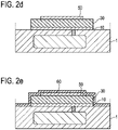
- patterning comprises a first step of patterning the second electrode layer 50 (see Fig. 2c ) and a second (separate) step of patterning the sacrificial layer 30 and the first electrode layer 10 (see Fig. 2d ).
- the sacrificial layer 30 and the first electrode layer 10 are patterned in a common step.
- the first step of patterning the second electrode layer 50 performed using a first etching mask (mask 1).
- the second patterning step can be performed using a second etching mask (mask 2).
- the second electrode layer 50 is patterned to be smaller than the first electrode layer 10 (e.g. in form of a ring electrode). Now, the step of patterning is finished.
- the method comprises depositing a dielectric layer 60 covering the deposited layers and films 10, 30, 50.
- This depositing step is again performed using Atomic Layer Deposition (ALD).
- ALD Atomic Layer Deposition
- the dielectric layer 60 covers the top surfaces and side surfaces of the deposited layers and films 10, 30, 50 with essentially the same coverage or thickness, as explained above. In this way, a very good step coverage is provided.
- the vertical portions of the dielectric layer 60 and the horizontal portions of the dielectric layer 60 have about the same coverage or thickness (see Fig. 2e ).
- the vertical portions of the dielectric layer 60 extend substantially orthogonal to the deposited layers 10, 30, 50.
- the method comprises removing the sacrificial layer 30 by providing an etch hole 32 (see Fig. 2f ) and etching the sacrificial layer 30 for forming the cavity 35 (see Fig. 2g ).
- the cavity 35 has a top surface 92, a bottom surface 94 and side surfaces 96, 98.
- the etch hole 32 is provided in the dielectric layer 60.
- the etch hole 32 can be provided using a third etching mask (mask 3).
- the cavity 35 is cleaned of any residues of the etching process.
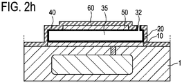
- first and second dielectric films 20, 40 are deposited in the cavity 35 by ALD ( Fig. 2h ).
- the first dielectric film 20 now covers the first electrode layer 10.
- the second dielectric film 40 covers the second electrode layer 50. Due to the ALD process in the cavity, not only the top and bottom surfaces 92, 94 are covered by the dielectric films but also the side surfaces 96, 98.
- an additional layer 70 in particular an additional dielectric layer, can be provided covering the dielectric layer 60.
- the additional layer 70 closes or seals the etch hole 32.
- the method comprises providing a conductive via 55 extending from the second electrode layer 50 in a direction orthogonal to the top surfaces of the layers.
- the conductive via 55 is orthogonal or at a right angle to the deposited layers.
- this is performed by providing an etch hole 62 (see Fig. 2j ) and filling the etch hole 62 with a conductive material for forming the conductive via 55 (see Fig. 2k ).
- Providing the etch hole 62 can be performed using a fourth etching mask (mask 4).
- the conductive via 15 to the first electrode 10 is formed in the substrate 1.
- a conductive portion 56 for providing an external electrical connection from the via 55 is provided. This can be performed by depositing a conductive layer on the additional layer 70 and then patterning the conductive layer. This can be performed using a fifth etching mask (mask 5).
- Fig. 2k shows a cross section of a CMUT 100 according to a second embodiment.
- the CMUT 100 of Fig. 2k has in particular been manufactured using the method as described above with reference to Fig. 2 .
- the CMUT 100 comprises the first electrode layer 10 on the substrate 1, the first dielectric film 20 on the first electrode layer 10, the cavity 35 formed above the first dielectric film 20, the second dielectric film 30 covering the cavity 35, and the second electrode layer 50 on the second dielectric film 40.
- the CMUT 100 may comprise a dielectric layer 11 on the substrate and a dielectric layer 51 on the second electrode layer 50, as explained with reference to the first embodiment.
- the CMUT 100 further comprises the dielectric layer 60 covering the deposited layers and films 10, 20, 30, 40, 50.
- the dielectric layer 60 covers the top surfaces and side surfaces of the deposited layers and films 10, 20, 30, 40, 50 with essentially the same coverage, as explained above.
- the vertical portions of the dielectric layer 60 extend substantially orthogonal to the deposited layers 10, 20, 30, 40, 50.
- the CMUT 100 further comprises the additional layer 70 covering the dielectric layer 60.
- the additional layer 70 is much thicker compared to the other layers or films for example more than 2 times or more, or more than 5 times or more (e.g. a thickness of layer 40 of about 200nm compared to a thickness of layer 70 of about 1 ⁇ m).
- the additional layer 70 is indicated only schematically, and that it can rather follow the shape of layer 60, similarly to the additional layer 70 illustrated with respect to Fig. 1k .
- the CMUT comprises the conductive via 55 extending from the second electrode layer 50 in the direction orthogonal to the top surfaces of the layers (vertical direction in Fig. 2j ).
- the CMUT 100 further comprises a conductive portion 56 for providing an external electrical connection from the via 55 (e.g. to an ASIC and/or a power supply, e.g. to connect to a bias voltage, or connections to a cable or wire bonds). Also, the CMUT 100 comprises the conductive via 15 from the first electrode 10.
- the conductive via 15 is formed in the substrate 1.
- the via 15, 55 extends in a vertical direction (orthogonal to the top surface(s) of the layers or the substrate) and the conductive portion 56 extends in a horizontal direction (parallel to the top surfaces(s) of the layers or the substrate).
- the first electrode layer 10 and the second electrode layer 50 may also be deposited subsequently to forming the cavity 35 by ALD in the already formed and cleaned cavity 35.
- the first electrode layer 10 and the second electrode layer 50 need not to be formed by patterning prior to the etching.
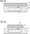
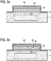
- Fig. 3a-i show a method of manufacturing a CMUT according to a third embodiment.
- the method of the third embodiment of Fig. 3a-h is similar to the method of the second embodiment of Fig.2a-k .
- the step of Fig. 2c of separately patterning the second electrode layer 50 is omitted. Therefore, in the third embodiment less etching masks are used.
- a substrate 1 comprises an ASIC 2 integrated therein and a conductive via 15 in the substrate 1.
- the method starts with depositing a first electrode layer 10 on the substrate 1.
- a sacrificial layer 30 is deposited on the first electrode layer 30.
- the sacrificial layer 30 is removable for forming a cavity of the transducer later on.
- a second electrode layer 50 is deposited on the sacrificial layer 30.
- Each of these depositing steps is performed by Atomic Layer Deposition (ALD).
- ALD Atomic Layer Deposition
- the method further comprises patterning all of the deposited layers and films 10, 30, 50, in particular all of the deposited CMUT functional layer 10, 30, 50.
- patterning comprises a common step of patterning the second electrode layer 50, the sacrificial layer 30, and the first electrode layer 10 (see Fig. 3b ).
- all of the deposited layers (second electrode layer 50, sacrificial layer 30 and first electrode layer 10) are patterned in a common step.
- all the deposited layers and films 10, 30, 50 have the same lateral dimension (in a direction parallel to the top surface(s) of the layers or substrate), for example diameter in the case of a circular shape.
- the common patterning step can be performed using a first etching mask (mask 1). Now, the step of patterning is finished.
- the method comprises depositing a dielectric layer 60 covering the deposited layers and films 10, 30, 50.
- This depositing step is again performed using Atomic Layer Deposition (ALD).
- ALD Atomic Layer Deposition
- the dielectric layer 60 covers the top surfaces and side surfaces of the deposited layers and films 10, 30, 50 with essentially the same coverage. In this way, a very good step coverage is provided. In other words, the vertical portions of the dielectric layer 60 and the horizontal portions of the dielectric layer 60 have about the same coverage or thickness (see Fig. 3c ).
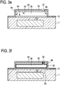
- the method comprises removing the sacrificial layer 30 by providing an etch hole 32 (see Fig. 3d ) and etching the sacrificial layer 30 for forming the cavity 35 (see Fig. 3e ).
- the cavity 35 has a top surface 92, a bottom surface 94 and side surfaces 96, 98.
- the etch hole 32 is provided in the dielectric layer 60.
- the etch hole 32 is preferably not provided in the second electrode layer 50, but somewhere next to it.
- the etch hole 32 extends from the dielectric layer 60, past the second electrode layer 50.
- the etch hole 32 can be provided using a second etching mask (mask 2). Subsequently, for removing the sacrificial layer 30 and forming the cavity 35, the cavity 35 is cleaned of any residues of the etching process. Then, first and second dielectric films 20, 40 are deposited in the cavity 35 by ALD ( Fig. 3f ). Hence, the first dielectric film 20 now covers the first electrode layer 10. The second dielectric film 40 covers the second electrode layer 50. Due to the ALD process in the cavity, not only the top and bottom surfaces 92, 94 are covered by the dielectric films but also the side surfaces 96, 98.
- an additional layer 70 in particular an additional dielectric layer, can be provided covering the dielectric layer 60.
- the additional layer 70 closes or seals the etch hole 32.
- the method comprises providing a conductive via 55 extending from the second electrode layer 50 in a direction orthogonal to the top surfaces of the layers.
- the conductive via 55 is orthogonal or at a right angle to the deposited layers.
- this is performed by providing an etch hole 62 (see Fig. 3h ) and filling the etch hole 62 with a conductive material for forming the conductive via 55 (see Fig. 3i ).
- Providing the etch hole 62 can be performed using a third etching mask (mask 3).
- the conductive via 15 to the first electrode 10 is formed in the substrate 1.
- a conductive portion 56 for providing an external electrical connection from the via 55 is provided. This can be performed by depositing a conductive layer on the additional layer 70 and then patterning the conductive layer. This can be performed using a fourth etching mask (mask 4).
- Fig. 3i shows a schematic cross section of a CMUT 100 according to a third embodiment.
- the CMUT 100 of Fig. 3h has in particular been manufactured using the method as described above with reference to Fig. 3 .
- the CMUT 100 comprises the first electrode layer 10 on the substrate 1, the first dielectric film 20 on the first electrode layer 10, the cavity 35 formed above the first dielectric film 20, the second dielectric film 30 covering the cavity 35, and the second electrode layer 50 on the second dielectric film 40.
- the CMUT 100 may comprise a dielectric layer 11 on the substrate and a dielectric layer 51 on the second electrode layer 50, as explained with reference to the first embodiment.
- Fig. 3i shows a schematic cross section of a CMUT 100 according to a third embodiment.
- the CMUT 100 of Fig. 3h has in particular been manufactured using the method as described above with reference to Fig. 3 .
- the CMUT 100 comprises the first electrode layer 10 on the substrate 1, the first dielectric film 20 on the first electrode layer 10, the
- the CMUT 100 further comprises the dielectric layer 60 covering the deposited layers and films 10, 20, 30, 40, 50.
- the dielectric layer 60 covers the top surfaces and side surfaces of the deposited layers and films 10, 20, 30, 40, 50 with essentially the same coverage, as explained above.
- the vertical portions of the dielectric layer 60 extend substantially orthogonal to the deposited layers 10, 20, 30, 40, 50.
- the CMUT 100 further comprises the additional layer 70 covering the dielectric layer 60.
- the additional layer 70 is much thicker compared to the other layers or films, for example more than 2 times or more, or more than 5 times or more (e.g. a thickness of layer 40 of about 200nm compared to a thickness of layer 70 of about 1 ⁇ m).
- the additional layer 70 is indicated only schematically, and that it can rather follow the shape of layer 60, similarly to the additional layer 70 illustrated with respect to Fig. 1k .
- the CMUT comprises the conductive via 55 extending from the second electrode layer 50 in the direction orthogonal to the top surfaces of the layers (vertical direction in Fig. 3i ).
- the CMUT 100 further comprises a conductive portion 56 for providing an external electrical connection from the via 55 (e.g. to an ASIC and/or a power supply, e.g. to connect to a bias voltage, or connections to a cable or wire bonds). Also, the CMUT 100 comprises the conductive via 15 from the first electrode 10.
- the conductive via 15 is formed in the substrate 1.
- the via 15, 55 extends in a vertical direction (orthogonal to the top surface(s) of the layers or the substrate) and the conductive portion extends in a horizontal direction (parallel to the top surfaces(s) of the layers or the substrate).
- the first electrode layer 10 and the second electrode layer 50 may also be deposited subsequently to forming the cavity 35 by ALD in the already formed and cleaned cavity 35.
- the first electrode layer 10 and the second electrode layer 50 need not to be formed by patterning prior to the etching.
- each of the first dielectric film 20 and the second dielectric film 40 comprises a first layer comprising an oxide, a second layer comprising a high-k material, and a third layer comprising an oxide.
- the dielectric isolation layer 20, 40 comprises an oxide layer (O), a high-k layer, and another oxide layer (O).
- a high-k layer is sandwiched between two oxide layers (in particular silicone oxide).
- the high-k material can be Aluminium Oxide (Al 2 O 3 ) and/or Hafnium Oxide (HfO 2 ).
- a laminate (alternating layers) of Oxide- Aluminium Oxide - Oxide (abbreviated by OAO) can be provided.
- the second layer comprises a first sublayer comprising Aluminium Oxide, a second sublayer comprising Hafnium Oxide, and a third sublayer comprising Aluminium Oxide.
- a laminate (alternating layers) of Oxide- Aluminium Oxide - Hafnium Oxide - Aluminium Oxide - Oxide (abbreviated by OAHAO) can be provided.
- the dielectric constant of the deposited layer generally depends on the density of the material, and thus the deposition or processing settings, such as the processing temperature (temperature at which the layer is formed).
- Aluminium Oxide has a dielectric constant (k or ⁇ r ) between 7 and 9, depending on the deposition or processing settings.
- the dielectric constant of Aluminium Oxide can be 7.5 (e.g. deposited at a low temperature of about 265°C), or 8 (e.g. deposited at a high temperature of about 350°C), or 9.
- Hafnium Oxide has a dielectric constant (k or ⁇ r ) between 12 and 27, depending on the deposition or processing settings.
- the dielectric constant of Hafnium Oxide can be 14, or 20, or 25.
- the dielectric constant of the laminate of Aluminium Oxide - Hafnium Oxide - Aluminium Oxide can for example be 10.
- each of the first electrode layer 10 and the second electrode layer 50 comprises a non-metal conductive material (e.g. a semiconductor).
- the non-metal conductive material can be at least one (or exactly one) material selected from the group comprising TiN (Titanium Nitride), TaN (Tantalum Nitride), TaCN, IrO 2 (Iridium Oxide), ITO (Indium Tin Oxide), LaNiO 3 , and SrRuO 3 (Strontium Ruthenate). These materials are suitable for Atomic Layer Deposition.
- the non-metal conductive material can be Titanium Nitride (TiN).
- Titanium Nitride has a conductivity of about 30 to 70 ⁇ cm, which is considered to be a good conductor.
- polysilicon can be used (having a conductivity in the order of 500 ⁇ cm).
- the material of the electrode layer can also be any other conductive material, such as for example a metal, in particular comprising at least one (or exactly one) material selected from the group comprising Ni (Nickel), Copper (Cu), W (Tungsten), Pt (Platinum), Ir (Iridium), and Al (Aluminium).
- the metal can be an alloy thereof.
- Aluminium has a conductivity in the order of 3 ⁇ cm.
- the conductive material of the electrode, metal and non-metal has to be suitable to be deposited by ALD (e.g. in an ALD-machine).
- the dielectric layer 60 and/or the additional layer 70 can for example be or comprise oxide (in particular silicon oxide), nitride (in particular silicon nitride), or a combination of both.
- the dielectric layer 60 can be or comprise a combination of (silicon) oxide and (silicon) nitride.
- the additional layer 70 can be or comprise (silicon) nitride.
- any other suitable dielectric material can be used.
- the dielectric layer 60 can for example be deposited by ALD or by PECVD.
- the additional layer 70 can in particular be deposited by PECVD, due to its higher thickness.
- the sacrificial layer 30 is made of a different material (having different etching properties) as the dielectric isolation layers 20, 40. In this way, the sacrificial layer can be removed selectively.
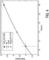
- Fig. 4 shows a diagram of a dielectric constant (epsilon) versus relative acoustic output pressure of a CMUT.
- Fig. 4 is based on a simulation. All dimensions (gap thickness, dielectric thickness, etc.) are assumed to be constant.
- the closed circle indicates Hafnium Oxide (HfO 2 ) deposited by ALD (here with an epsilon of 14).
- the open circle indicates ONO.
- the diamond indicates Aluminium Oxide (Al 2 O 3 ) deposited by ALD (here with an epsilon of 8).
- high-k materials almost double the output pressure (e.g. about 70% for Al 2 O 3 ), provided the bias voltage can be applied.
- Fig. 5 shows an exemplary graph of the electrical field across the dielectric versus current flowing through the dielectric. Graphs of the field versus current are shown for each of ONO and Aluminium Oxide Al 2 O 3 at high temperature. As can be seen in Fig. 8, for the same field value, Aluminium Oxide Al 2 O 3 (at high temperature) has less leakage current, compared to ONO. Also, for Aluminium Oxide Al 2 O 3 (at high temperature) at least the same bias voltage can be applied compared to ONO.
- ALD Atomic Layer Deposition
- a ll L ayer ALD (AL-ALD) CMUT process is very beneficial because it offers options to further improve the CMUT performance by tuning the properties of the individual layers and their interfaces.
- the AL-ALD technique with top-to-bottom patterning ensures high quality interfaces of the various dielectrics and requires less operator intervention.
- the first dielectric film 20 and/or the second dielectric film 40 comprises process residuals, such as Carbon or Chlorine residuals.
- the residuals can for example be detected using XPS (X-ray photoelectron spectroscopy) or other characterization methods, such as SIMS (Secondary Ion Mass spectroscopy).
- the second layer of the dielectric isolation layer 20, 40 has a thickness below 100nm. Such a very thin high-k layer can (only) be provided using ALD.
- a layer (in particular of Al 2 O 3 and/or HfO 2 ) deposited by ALD can exhibit one or more of the following features:
- SIMS Single Ion Mass spectroscopy
- ALD Aluminum-Oxide deposited by ALD.
- Argon is used and some remainders are found in the sputtered layer (e.g. a few percent). This can be easily detected by SIMS (Secondary Ion Mass spectroscopy).
- the functionality of the oxide layer (O) in an OAO dielectric isolation layer is very different, compared to the oxide layer (O) in an ONO dielectric isolation layer.
- the oxide layer (O) in an ONO dielectric isolation layer is there for electrical reasons. Without the oxide layer (O), there would be a significant electrical charging of the CMUT device that seriously degrades the performance.
- the minimum thickness of a single O-layer (deposited by PECVD) is about 50 nm.
- the oxide layer (O) in an ONO dielectric isolation layer is there for processing reasons. It was found that without the oxide layer (i.e. an Alumina-layer only), the layer suffers from very large mechanical stress resulting is an extreme membrane deformation and the CMUT device is not operable.
- using an OAO dielectric isolation layer provides a low stress level.
- the oxide layer can be thin. Further, an OAO dielectric isolation layer has an even better electrical behaviour compared to an Alumina-layer only.
- the capacitive micro-machined transducer has been described as a CMUT, involving ultrasound. However, it shall be understood that the capacitive micro-machined transducer can also be used for other applications, for example as a pressure sensor or pressure transducer.
- the capacitive micro-machined transducer in particular CMUT, can comprise or be a single cell, in particular CMUT cell. However, it will be understood that the capacitive micro-machined transducer, in particular CMUT, can also comprise a plurality or an array of cells, in particular CMUT cells.
- the capacitive micro-machined transducer, in particular CMUT, and/or its layers can have a circular shape. However, also other shapes can be used, such as a square or a hexagonal shape.
Applications Claiming Priority (2)
| Application Number | Priority Date | Filing Date | Title |
|---|---|---|---|
| US201261728339P | 2012-11-20 | 2012-11-20 | |
| PCT/IB2013/059932 WO2014080310A2 (en) | 2012-11-20 | 2013-11-06 | Capacitive micro-machined transducer and method of manufacturing the same |
Publications (2)
| Publication Number | Publication Date |
|---|---|
| EP2922707A2 EP2922707A2 (en) | 2015-09-30 |
| EP2922707B1 true EP2922707B1 (en) | 2022-04-27 |
Family
ID=49596362
Family Applications (1)
| Application Number | Title | Priority Date | Filing Date |
|---|---|---|---|
| EP13792500.4A Active EP2922707B1 (en) | 2012-11-20 | 2013-11-06 | Capacitive micro-machined transducer and method of manufacturing the same |
Country Status (5)
| Country | Link |
|---|---|
| US (1) | US9607606B2 (ja) |
| EP (1) | EP2922707B1 (ja) |
| JP (1) | JP6328131B2 (ja) |
| CN (1) | CN104812504B (ja) |
| WO (1) | WO2014080310A2 (ja) |
Families Citing this family (5)
| Publication number | Priority date | Publication date | Assignee | Title |
|---|---|---|---|---|
| CN104023860B (zh) * | 2011-12-20 | 2016-06-15 | 皇家飞利浦有限公司 | 超声换能器设备及制造所述超声换能器设备的方法 |
| JP6416232B2 (ja) * | 2013-09-24 | 2018-10-31 | コーニンクレッカ フィリップス エヌ ヴェKoninklijke Philips N.V. | Cmutデバイス製造方法、cmutデバイス、及び装置 |
| DE102015102300A1 (de) * | 2015-02-18 | 2016-08-18 | Osram Opto Semiconductors Gmbh | Verfahren zum Herstellen eines elektronischen Bauelements |
| US9957393B2 (en) | 2015-03-30 | 2018-05-01 | Enzo Biochem, Inc. | Monoazo dyes with cyclic amine as fluorescence quenchers |
| US20210403321A1 (en) * | 2020-06-30 | 2021-12-30 | Butterfly Network, Inc. | Formation of self-assembled monolayer for ultrasonic transducers |
Citations (1)
| Publication number | Priority date | Publication date | Assignee | Title |
|---|---|---|---|---|
| US20070057600A1 (en) * | 2005-09-09 | 2007-03-15 | Hiroshi Fukuda | Ultrasonic transducer and manufacturing method thereof |
Family Cites Families (12)
| Publication number | Priority date | Publication date | Assignee | Title |
|---|---|---|---|---|
| WO2005077012A2 (en) * | 2004-02-06 | 2005-08-25 | Georgia Tech Research Corporation | Cmut devices and fabrication methods |
| CN101589543B (zh) * | 2005-05-18 | 2012-10-31 | 科隆科技公司 | 微机电换能器 |
| EP1914800A1 (en) * | 2006-10-20 | 2008-04-23 | Interuniversitair Microelektronica Centrum | Method of manufacturing a semiconductor device with multiple dielectrics |
| US7733552B2 (en) * | 2007-03-21 | 2010-06-08 | Qualcomm Mems Technologies, Inc | MEMS cavity-coating layers and methods |
| US7892176B2 (en) * | 2007-05-02 | 2011-02-22 | General Electric Company | Monitoring or imaging system with interconnect structure for large area sensor array |
| US20090275198A1 (en) * | 2008-05-01 | 2009-11-05 | Smuruthi Kamepalli | Vapor Phase Methods for Forming Electrodes in Phase Change Memory Devices |
| CN102159334A (zh) * | 2008-09-16 | 2011-08-17 | 皇家飞利浦电子股份有限公司 | 电容性微机械加工的超声换能器 |
| JP2011023658A (ja) * | 2009-07-17 | 2011-02-03 | Fuji Electric Systems Co Ltd | 半導体装置の製造方法 |
| US20110065276A1 (en) * | 2009-09-11 | 2011-03-17 | Applied Materials, Inc. | Apparatus and Methods for Cyclical Oxidation and Etching |
| WO2011142850A2 (en) * | 2010-01-22 | 2011-11-17 | The Regents Of The University Of California | Etchant-free methods of producing a gap between two layers, and devices produced thereby |
| JP2012080095A (ja) * | 2010-09-10 | 2012-04-19 | Elpida Memory Inc | 半導体装置及びその製造方法 |
| JP5677016B2 (ja) * | 2010-10-15 | 2015-02-25 | キヤノン株式会社 | 電気機械変換装置及びその作製方法 |
-
2013
- 2013-11-06 EP EP13792500.4A patent/EP2922707B1/en active Active
- 2013-11-06 WO PCT/IB2013/059932 patent/WO2014080310A2/en active Application Filing
- 2013-11-06 JP JP2015542385A patent/JP6328131B2/ja not_active Expired - Fee Related
- 2013-11-06 CN CN201380060566.7A patent/CN104812504B/zh active Active
- 2013-11-06 US US14/443,159 patent/US9607606B2/en active Active
Patent Citations (1)
| Publication number | Priority date | Publication date | Assignee | Title |
|---|---|---|---|---|
| US20070057600A1 (en) * | 2005-09-09 | 2007-03-15 | Hiroshi Fukuda | Ultrasonic transducer and manufacturing method thereof |
Also Published As
| Publication number | Publication date |
|---|---|
| CN104812504B (zh) | 2018-01-26 |
| EP2922707A2 (en) | 2015-09-30 |
| WO2014080310A2 (en) | 2014-05-30 |
| US20150294663A1 (en) | 2015-10-15 |
| JP2015536622A (ja) | 2015-12-21 |
| CN104812504A (zh) | 2015-07-29 |
| JP6328131B2 (ja) | 2018-05-23 |
| WO2014080310A3 (en) | 2014-11-27 |
| US9607606B2 (en) | 2017-03-28 |
Similar Documents
| Publication | Publication Date | Title |
|---|---|---|
| EP2806982B1 (en) | Capacitive micro-machined transducer and method of manufacturing the same | |
| EP2806983B1 (en) | Capacitive micro-machined transducer and method of manufacturing the same | |
| EP2922707B1 (en) | Capacitive micro-machined transducer and method of manufacturing the same | |
| US8288192B2 (en) | Method of manufacturing a capacitive electromechanical transducer | |
| JP4492821B2 (ja) | 圧電素子 | |
| US11329098B2 (en) | Piezoelectric micromachined ultrasonic transducers and methods for fabricating thereof | |
| EP3306951A2 (en) | Microphone and method for manufacturing the same | |
| TWI654781B (zh) | 壓電式層裝置的製造方法以及相關的壓電式層裝置 | |
| US9214622B2 (en) | Size-controllable opening and method of making same | |
| US8053951B2 (en) | Thin film piezoelectric actuators | |
| Howell | Dielectric Actuation Techniques at the Nanoscale: Piezoelectricity and Flexoelectricity |
Legal Events
| Date | Code | Title | Description |
|---|---|---|---|
| PUAI | Public reference made under article 153(3) epc to a published international application that has entered the european phase |
Free format text: ORIGINAL CODE: 0009012 |
|
| 17P | Request for examination filed |
Effective date: 20150622 |
|
| AK | Designated contracting states |
Kind code of ref document: A2 Designated state(s): AL AT BE BG CH CY CZ DE DK EE ES FI FR GB GR HR HU IE IS IT LI LT LU LV MC MK MT NL NO PL PT RO RS SE SI SK SM TR |
|
| AX | Request for extension of the european patent |
Extension state: BA ME |
|
| DAX | Request for extension of the european patent (deleted) | ||
| STAA | Information on the status of an ep patent application or granted ep patent |
Free format text: STATUS: EXAMINATION IS IN PROGRESS |
|
| 17Q | First examination report despatched |
Effective date: 20191011 |
|
| RAP1 | Party data changed (applicant data changed or rights of an application transferred) |
Owner name: KONINKLIJKE PHILIPS N.V. |
|
| STAA | Information on the status of an ep patent application or granted ep patent |
Free format text: STATUS: EXAMINATION IS IN PROGRESS |
|
| REG | Reference to a national code |
Ref country code: DE Ref legal event code: R079 Ref document number: 602013081513 Country of ref document: DE Free format text: PREVIOUS MAIN CLASS: B60B0001020000 Ipc: B06B0001020000 |
|
| GRAP | Despatch of communication of intention to grant a patent |
Free format text: ORIGINAL CODE: EPIDOSNIGR1 |
|
| STAA | Information on the status of an ep patent application or granted ep patent |
Free format text: STATUS: GRANT OF PATENT IS INTENDED |
|
| RIC1 | Information provided on ipc code assigned before grant |
Ipc: B06B 1/02 20060101AFI20211101BHEP |
|
| INTG | Intention to grant announced |
Effective date: 20211129 |
|
| GRAS | Grant fee paid |
Free format text: ORIGINAL CODE: EPIDOSNIGR3 |
|
| GRAA | (expected) grant |
Free format text: ORIGINAL CODE: 0009210 |
|
| STAA | Information on the status of an ep patent application or granted ep patent |
Free format text: STATUS: THE PATENT HAS BEEN GRANTED |
|
| AK | Designated contracting states |
Kind code of ref document: B1 Designated state(s): AL AT BE BG CH CY CZ DE DK EE ES FI FR GB GR HR HU IE IS IT LI LT LU LV MC MK MT NL NO PL PT RO RS SE SI SK SM TR |
|
| REG | Reference to a national code |
Ref country code: GB Ref legal event code: FG4D |
|
| REG | Reference to a national code |
Ref country code: CH Ref legal event code: EP |
|
| REG | Reference to a national code |
Ref country code: DE Ref legal event code: R096 Ref document number: 602013081513 Country of ref document: DE |
|
| REG | Reference to a national code |
Ref country code: AT Ref legal event code: REF Ref document number: 1486523 Country of ref document: AT Kind code of ref document: T Effective date: 20220515 |
|
| REG | Reference to a national code |
Ref country code: IE Ref legal event code: FG4D |
|
| REG | Reference to a national code |
Ref country code: DE Ref legal event code: R084 Ref document number: 602013081513 Country of ref document: DE |
|
| REG | Reference to a national code |
Ref country code: GB Ref legal event code: 746 Effective date: 20220624 |
|
| REG | Reference to a national code |
Ref country code: LT Ref legal event code: MG9D |
|
| REG | Reference to a national code |
Ref country code: NL Ref legal event code: MP Effective date: 20220427 |
|
| REG | Reference to a national code |
Ref country code: AT Ref legal event code: MK05 Ref document number: 1486523 Country of ref document: AT Kind code of ref document: T Effective date: 20220427 |
|
| PG25 | Lapsed in a contracting state [announced via postgrant information from national office to epo] |
Ref country code: NL Free format text: LAPSE BECAUSE OF FAILURE TO SUBMIT A TRANSLATION OF THE DESCRIPTION OR TO PAY THE FEE WITHIN THE PRESCRIBED TIME-LIMIT Effective date: 20220427 |
|
| PG25 | Lapsed in a contracting state [announced via postgrant information from national office to epo] |
Ref country code: SE Free format text: LAPSE BECAUSE OF FAILURE TO SUBMIT A TRANSLATION OF THE DESCRIPTION OR TO PAY THE FEE WITHIN THE PRESCRIBED TIME-LIMIT Effective date: 20220427 Ref country code: PT Free format text: LAPSE BECAUSE OF FAILURE TO SUBMIT A TRANSLATION OF THE DESCRIPTION OR TO PAY THE FEE WITHIN THE PRESCRIBED TIME-LIMIT Effective date: 20220829 Ref country code: NO Free format text: LAPSE BECAUSE OF FAILURE TO SUBMIT A TRANSLATION OF THE DESCRIPTION OR TO PAY THE FEE WITHIN THE PRESCRIBED TIME-LIMIT Effective date: 20220727 Ref country code: LT Free format text: LAPSE BECAUSE OF FAILURE TO SUBMIT A TRANSLATION OF THE DESCRIPTION OR TO PAY THE FEE WITHIN THE PRESCRIBED TIME-LIMIT Effective date: 20220427 Ref country code: HR Free format text: LAPSE BECAUSE OF FAILURE TO SUBMIT A TRANSLATION OF THE DESCRIPTION OR TO PAY THE FEE WITHIN THE PRESCRIBED TIME-LIMIT Effective date: 20220427 Ref country code: GR Free format text: LAPSE BECAUSE OF FAILURE TO SUBMIT A TRANSLATION OF THE DESCRIPTION OR TO PAY THE FEE WITHIN THE PRESCRIBED TIME-LIMIT Effective date: 20220728 Ref country code: FI Free format text: LAPSE BECAUSE OF FAILURE TO SUBMIT A TRANSLATION OF THE DESCRIPTION OR TO PAY THE FEE WITHIN THE PRESCRIBED TIME-LIMIT Effective date: 20220427 Ref country code: ES Free format text: LAPSE BECAUSE OF FAILURE TO SUBMIT A TRANSLATION OF THE DESCRIPTION OR TO PAY THE FEE WITHIN THE PRESCRIBED TIME-LIMIT Effective date: 20220427 Ref country code: BG Free format text: LAPSE BECAUSE OF FAILURE TO SUBMIT A TRANSLATION OF THE DESCRIPTION OR TO PAY THE FEE WITHIN THE PRESCRIBED TIME-LIMIT Effective date: 20220727 Ref country code: AT Free format text: LAPSE BECAUSE OF FAILURE TO SUBMIT A TRANSLATION OF THE DESCRIPTION OR TO PAY THE FEE WITHIN THE PRESCRIBED TIME-LIMIT Effective date: 20220427 |
|
| PG25 | Lapsed in a contracting state [announced via postgrant information from national office to epo] |
Ref country code: RS Free format text: LAPSE BECAUSE OF FAILURE TO SUBMIT A TRANSLATION OF THE DESCRIPTION OR TO PAY THE FEE WITHIN THE PRESCRIBED TIME-LIMIT Effective date: 20220427 Ref country code: PL Free format text: LAPSE BECAUSE OF FAILURE TO SUBMIT A TRANSLATION OF THE DESCRIPTION OR TO PAY THE FEE WITHIN THE PRESCRIBED TIME-LIMIT Effective date: 20220427 Ref country code: LV Free format text: LAPSE BECAUSE OF FAILURE TO SUBMIT A TRANSLATION OF THE DESCRIPTION OR TO PAY THE FEE WITHIN THE PRESCRIBED TIME-LIMIT Effective date: 20220427 Ref country code: IS Free format text: LAPSE BECAUSE OF FAILURE TO SUBMIT A TRANSLATION OF THE DESCRIPTION OR TO PAY THE FEE WITHIN THE PRESCRIBED TIME-LIMIT Effective date: 20220827 |
|
| REG | Reference to a national code |
Ref country code: DE Ref legal event code: R097 Ref document number: 602013081513 Country of ref document: DE |
|
| PG25 | Lapsed in a contracting state [announced via postgrant information from national office to epo] |
Ref country code: SM Free format text: LAPSE BECAUSE OF FAILURE TO SUBMIT A TRANSLATION OF THE DESCRIPTION OR TO PAY THE FEE WITHIN THE PRESCRIBED TIME-LIMIT Effective date: 20220427 Ref country code: SK Free format text: LAPSE BECAUSE OF FAILURE TO SUBMIT A TRANSLATION OF THE DESCRIPTION OR TO PAY THE FEE WITHIN THE PRESCRIBED TIME-LIMIT Effective date: 20220427 Ref country code: RO Free format text: LAPSE BECAUSE OF FAILURE TO SUBMIT A TRANSLATION OF THE DESCRIPTION OR TO PAY THE FEE WITHIN THE PRESCRIBED TIME-LIMIT Effective date: 20220427 Ref country code: EE Free format text: LAPSE BECAUSE OF FAILURE TO SUBMIT A TRANSLATION OF THE DESCRIPTION OR TO PAY THE FEE WITHIN THE PRESCRIBED TIME-LIMIT Effective date: 20220427 Ref country code: DK Free format text: LAPSE BECAUSE OF FAILURE TO SUBMIT A TRANSLATION OF THE DESCRIPTION OR TO PAY THE FEE WITHIN THE PRESCRIBED TIME-LIMIT Effective date: 20220427 Ref country code: CZ Free format text: LAPSE BECAUSE OF FAILURE TO SUBMIT A TRANSLATION OF THE DESCRIPTION OR TO PAY THE FEE WITHIN THE PRESCRIBED TIME-LIMIT Effective date: 20220427 |
|
| PGFP | Annual fee paid to national office [announced via postgrant information from national office to epo] |
Ref country code: GB Payment date: 20221122 Year of fee payment: 10 Ref country code: FR Payment date: 20221122 Year of fee payment: 10 |
|
| PLBE | No opposition filed within time limit |
Free format text: ORIGINAL CODE: 0009261 |
|
| STAA | Information on the status of an ep patent application or granted ep patent |
Free format text: STATUS: NO OPPOSITION FILED WITHIN TIME LIMIT |
|
| PG25 | Lapsed in a contracting state [announced via postgrant information from national office to epo] |
Ref country code: AL Free format text: LAPSE BECAUSE OF FAILURE TO SUBMIT A TRANSLATION OF THE DESCRIPTION OR TO PAY THE FEE WITHIN THE PRESCRIBED TIME-LIMIT Effective date: 20220427 |
|
| 26N | No opposition filed |
Effective date: 20230130 |
|
| PG25 | Lapsed in a contracting state [announced via postgrant information from national office to epo] |
Ref country code: SI Free format text: LAPSE BECAUSE OF FAILURE TO SUBMIT A TRANSLATION OF THE DESCRIPTION OR TO PAY THE FEE WITHIN THE PRESCRIBED TIME-LIMIT Effective date: 20220427 |
|
| PG25 | Lapsed in a contracting state [announced via postgrant information from national office to epo] |
Ref country code: MC Free format text: LAPSE BECAUSE OF FAILURE TO SUBMIT A TRANSLATION OF THE DESCRIPTION OR TO PAY THE FEE WITHIN THE PRESCRIBED TIME-LIMIT Effective date: 20220427 |
|
| REG | Reference to a national code |
Ref country code: CH Ref legal event code: PL |
|
| REG | Reference to a national code |
Ref country code: BE Ref legal event code: MM Effective date: 20221130 |
|
| PG25 | Lapsed in a contracting state [announced via postgrant information from national office to epo] |
Ref country code: LI Free format text: LAPSE BECAUSE OF NON-PAYMENT OF DUE FEES Effective date: 20221130 Ref country code: CH Free format text: LAPSE BECAUSE OF NON-PAYMENT OF DUE FEES Effective date: 20221130 |
|
| PG25 | Lapsed in a contracting state [announced via postgrant information from national office to epo] |
Ref country code: LU Free format text: LAPSE BECAUSE OF NON-PAYMENT OF DUE FEES Effective date: 20221106 |
|
| PG25 | Lapsed in a contracting state [announced via postgrant information from national office to epo] |
Ref country code: IE Free format text: LAPSE BECAUSE OF NON-PAYMENT OF DUE FEES Effective date: 20221106 |
|
| PG25 | Lapsed in a contracting state [announced via postgrant information from national office to epo] |
Ref country code: BE Free format text: LAPSE BECAUSE OF NON-PAYMENT OF DUE FEES Effective date: 20221130 |
|
| PG25 | Lapsed in a contracting state [announced via postgrant information from national office to epo] |
Ref country code: IT Free format text: LAPSE BECAUSE OF FAILURE TO SUBMIT A TRANSLATION OF THE DESCRIPTION OR TO PAY THE FEE WITHIN THE PRESCRIBED TIME-LIMIT Effective date: 20220427 |
|
| PGFP | Annual fee paid to national office [announced via postgrant information from national office to epo] |
Ref country code: DE Payment date: 20231127 Year of fee payment: 11 |
|
| PG25 | Lapsed in a contracting state [announced via postgrant information from national office to epo] |
Ref country code: HU Free format text: LAPSE BECAUSE OF FAILURE TO SUBMIT A TRANSLATION OF THE DESCRIPTION OR TO PAY THE FEE WITHIN THE PRESCRIBED TIME-LIMIT; INVALID AB INITIO Effective date: 20131106 |
|
| PG25 | Lapsed in a contracting state [announced via postgrant information from national office to epo] |
Ref country code: CY Free format text: LAPSE BECAUSE OF FAILURE TO SUBMIT A TRANSLATION OF THE DESCRIPTION OR TO PAY THE FEE WITHIN THE PRESCRIBED TIME-LIMIT Effective date: 20220427 |