EP2911486A1 - PCB-based connector device - Google Patents
PCB-based connector device Download PDFInfo
- Publication number
- EP2911486A1 EP2911486A1 EP14290041.4A EP14290041A EP2911486A1 EP 2911486 A1 EP2911486 A1 EP 2911486A1 EP 14290041 A EP14290041 A EP 14290041A EP 2911486 A1 EP2911486 A1 EP 2911486A1
- Authority
- EP
- European Patent Office
- Prior art keywords
- printed circuit
- circuit board
- electrically conductive
- connector device
- connector
- Prior art date
- Legal status (The legal status is an assumption and is not a legal conclusion. Google has not performed a legal analysis and makes no representation as to the accuracy of the status listed.)
- Granted
Links
Images


Classifications
-
- H—ELECTRICITY
- H01—ELECTRIC ELEMENTS
- H01R—ELECTRICALLY-CONDUCTIVE CONNECTIONS; STRUCTURAL ASSOCIATIONS OF A PLURALITY OF MUTUALLY-INSULATED ELECTRICAL CONNECTING ELEMENTS; COUPLING DEVICES; CURRENT COLLECTORS
- H01R13/00—Details of coupling devices of the kinds covered by groups H01R12/70 or H01R24/00 - H01R33/00
- H01R13/66—Structural association with built-in electrical component
- H01R13/665—Structural association with built-in electrical component with built-in electronic circuit
-
- H—ELECTRICITY
- H01—ELECTRIC ELEMENTS
- H01R—ELECTRICALLY-CONDUCTIVE CONNECTIONS; STRUCTURAL ASSOCIATIONS OF A PLURALITY OF MUTUALLY-INSULATED ELECTRICAL CONNECTING ELEMENTS; COUPLING DEVICES; CURRENT COLLECTORS
- H01R12/00—Structural associations of a plurality of mutually-insulated electrical connecting elements, specially adapted for printed circuits, e.g. printed circuit boards [PCB], flat or ribbon cables, or like generally planar structures, e.g. terminal strips, terminal blocks; Coupling devices specially adapted for printed circuits, flat or ribbon cables, or like generally planar structures; Terminals specially adapted for contact with, or insertion into, printed circuits, flat or ribbon cables, or like generally planar structures
- H01R12/70—Coupling devices
- H01R12/71—Coupling devices for rigid printing circuits or like structures
- H01R12/72—Coupling devices for rigid printing circuits or like structures coupling with the edge of the rigid printed circuits or like structures
- H01R12/721—Coupling devices for rigid printing circuits or like structures coupling with the edge of the rigid printed circuits or like structures cooperating directly with the edge of the rigid printed circuits
-
- H—ELECTRICITY
- H01—ELECTRIC ELEMENTS
- H01R—ELECTRICALLY-CONDUCTIVE CONNECTIONS; STRUCTURAL ASSOCIATIONS OF A PLURALITY OF MUTUALLY-INSULATED ELECTRICAL CONNECTING ELEMENTS; COUPLING DEVICES; CURRENT COLLECTORS
- H01R12/00—Structural associations of a plurality of mutually-insulated electrical connecting elements, specially adapted for printed circuits, e.g. printed circuit boards [PCB], flat or ribbon cables, or like generally planar structures, e.g. terminal strips, terminal blocks; Coupling devices specially adapted for printed circuits, flat or ribbon cables, or like generally planar structures; Terminals specially adapted for contact with, or insertion into, printed circuits, flat or ribbon cables, or like generally planar structures
- H01R12/70—Coupling devices
- H01R12/71—Coupling devices for rigid printing circuits or like structures
- H01R12/72—Coupling devices for rigid printing circuits or like structures coupling with the edge of the rigid printed circuits or like structures
- H01R12/73—Coupling devices for rigid printing circuits or like structures coupling with the edge of the rigid printed circuits or like structures connecting to other rigid printed circuits or like structures
- H01R12/732—Printed circuits being in the same plane
-
- H—ELECTRICITY
- H05—ELECTRIC TECHNIQUES NOT OTHERWISE PROVIDED FOR
- H05K—PRINTED CIRCUITS; CASINGS OR CONSTRUCTIONAL DETAILS OF ELECTRIC APPARATUS; MANUFACTURE OF ASSEMBLAGES OF ELECTRICAL COMPONENTS
- H05K1/00—Printed circuits
- H05K1/02—Details
- H05K1/11—Printed elements for providing electric connections to or between printed circuits
- H05K1/117—Pads along the edge of rigid circuit boards, e.g. for pluggable connectors
-
- H—ELECTRICITY
- H05—ELECTRIC TECHNIQUES NOT OTHERWISE PROVIDED FOR
- H05K—PRINTED CIRCUITS; CASINGS OR CONSTRUCTIONAL DETAILS OF ELECTRIC APPARATUS; MANUFACTURE OF ASSEMBLAGES OF ELECTRICAL COMPONENTS
- H05K1/00—Printed circuits
- H05K1/02—Details
- H05K1/14—Structural association of two or more printed circuits
- H05K1/142—Arrangements of planar printed circuit boards in the same plane, e.g. auxiliary printed circuit insert mounted in a main printed circuit
-
- H—ELECTRICITY
- H05—ELECTRIC TECHNIQUES NOT OTHERWISE PROVIDED FOR
- H05K—PRINTED CIRCUITS; CASINGS OR CONSTRUCTIONAL DETAILS OF ELECTRIC APPARATUS; MANUFACTURE OF ASSEMBLAGES OF ELECTRICAL COMPONENTS
- H05K1/00—Printed circuits
- H05K1/18—Printed circuits structurally associated with non-printed electric components
- H05K1/182—Printed circuits structurally associated with non-printed electric components associated with components mounted in printed circuit boards [PCB], e.g. insert-mounted components [IMC]
- H05K1/185—Printed circuits structurally associated with non-printed electric components associated with components mounted in printed circuit boards [PCB], e.g. insert-mounted components [IMC] associated with components encapsulated in the insulating substrate of the PCBs; associated with components incorporated in internal layers of multilayer circuit boards
-
- H—ELECTRICITY
- H05—ELECTRIC TECHNIQUES NOT OTHERWISE PROVIDED FOR
- H05K—PRINTED CIRCUITS; CASINGS OR CONSTRUCTIONAL DETAILS OF ELECTRIC APPARATUS; MANUFACTURE OF ASSEMBLAGES OF ELECTRICAL COMPONENTS
- H05K2201/00—Indexing scheme relating to printed circuits covered by H05K1/00
- H05K2201/04—Assemblies of printed circuits
- H05K2201/042—Stacked spaced PCBs; Planar parts of folded flexible circuits having mounted components in between or spaced from each other
-
- H—ELECTRICITY
- H05—ELECTRIC TECHNIQUES NOT OTHERWISE PROVIDED FOR
- H05K—PRINTED CIRCUITS; CASINGS OR CONSTRUCTIONAL DETAILS OF ELECTRIC APPARATUS; MANUFACTURE OF ASSEMBLAGES OF ELECTRICAL COMPONENTS
- H05K2201/00—Indexing scheme relating to printed circuits covered by H05K1/00
- H05K2201/09—Shape and layout
- H05K2201/09145—Edge details
- H05K2201/09163—Slotted edge
-
- H—ELECTRICITY
- H05—ELECTRIC TECHNIQUES NOT OTHERWISE PROVIDED FOR
- H05K—PRINTED CIRCUITS; CASINGS OR CONSTRUCTIONAL DETAILS OF ELECTRIC APPARATUS; MANUFACTURE OF ASSEMBLAGES OF ELECTRICAL COMPONENTS
- H05K2201/00—Indexing scheme relating to printed circuits covered by H05K1/00
- H05K2201/20—Details of printed circuits not provided for in H05K2201/01 - H05K2201/10
- H05K2201/209—Auto-mechanical connection between a component and a PCB or between two PCBs
-
- H—ELECTRICITY
- H05—ELECTRIC TECHNIQUES NOT OTHERWISE PROVIDED FOR
- H05K—PRINTED CIRCUITS; CASINGS OR CONSTRUCTIONAL DETAILS OF ELECTRIC APPARATUS; MANUFACTURE OF ASSEMBLAGES OF ELECTRICAL COMPONENTS
- H05K3/00—Apparatus or processes for manufacturing printed circuits
- H05K3/46—Manufacturing multilayer circuits
- H05K3/4697—Manufacturing multilayer circuits having cavities, e.g. for mounting components
-
- H—ELECTRICITY
- H10—SEMICONDUCTOR DEVICES; ELECTRIC SOLID-STATE DEVICES NOT OTHERWISE PROVIDED FOR
- H10W—GENERIC PACKAGES, INTERCONNECTIONS, CONNECTORS OR OTHER CONSTRUCTIONAL DETAILS OF DEVICES COVERED BY CLASS H10
- H10W70/00—Package substrates; Interposers; Redistribution layers [RDL]
- H10W70/60—Insulating or insulated package substrates; Interposers; Redistribution layers
-
- H—ELECTRICITY
- H10—SEMICONDUCTOR DEVICES; ELECTRIC SOLID-STATE DEVICES NOT OTHERWISE PROVIDED FOR
- H10W—GENERIC PACKAGES, INTERCONNECTIONS, CONNECTORS OR OTHER CONSTRUCTIONAL DETAILS OF DEVICES COVERED BY CLASS H10
- H10W72/00—Interconnections or connectors in packages
- H10W72/90—Bond pads, in general
- H10W72/941—Dispositions of bond pads
- H10W72/9413—Dispositions of bond pads on encapsulations
Definitions
- the invention relates to a connector device for connection with a counter piece for establishing a mechanical and electric connection.
- the invention relates to a connection arrangement.
- the invention relates to a method of manufacturing a connector device.
- Standard connectors generally constitute of metal inserts (i.e. contacts) surrounded by a polymer. Such an assembly is often created during a moulding process (such as injection moulding, transfer moulding, etc.). This method allows the creation of complex mechanical shapes, with a variety of physical properties depending on the selected material combination.
- US 5,374,196 and US 5,515,604 disclose laminated connectors which comprise a plurality of layers of rigid dielectric material which are laminated together.
- the dielectric contains traces which are joined to contact pads, connecting the traces to adjacent circuit boards.
- the rigid dielectric layers contain recesses where the contact pads are placed.
- Cross-traces can be placed on each individual layer of dielectric or vias made through the dielectric layers, to interconnect traces.
- a connector device for connection with a counter piece for establishing a mechanical and electric connection, a connection arrangement, and a method of manufacturing a connector device according to the independent claims are provided.
- a connector device for connection with a counter piece for establishing a mechanical and electric connection comprising at least two printed circuit board (PCB) elements or sections each comprising an electrically insulating core and at least one comprising an electrically conductive structure at least partially on the respective electrically insulating core, wherein the at least one electrically conductive structure is arranged at least partially on an exposed surface of the connector device and is configured for establishing the electric connection with the counter piece upon establishing the mechanical connection with the counter piece.
- PCB printed circuit board
- connection arrangement comprises a connector device having the above mentioned features for connection with a counter piece, and the counter piece being configured for being mechanically and electrically connected with the connector device upon plugging the counter piece and the connector device together.
- a method of manufacturing a connector device for connection with a counter piece for establishing a mechanical and electric connection comprises forming at least one printed circuit board (PCB) element as a subsection of a printed circuit board (PCB) and comprising an electrically insulating core and an electrically conductive structure at least partially on the electrically insulating core, arranging at least part of the electrically conductive structure on an exposed surface (of the connector device to be manufactured), and configuring the electrically conductive structure for establishing the electric connection with the counter piece upon establishing the mechanical connection between the connector device and the counter piece.
- PCB printed circuit board
- PCB printed circuit board
- a "printed circuit board” may denote a board of an electrically insulting core covered with electrically conductive material and conventionally serving for mounting thereon electronic members (such as packaged electronic chips, sockets, etc.) to be electrically coupled by the electrically conductive material. More specifically, a PCB may mechanically support and electrically connect electronic components using conductive tracks, pads and other features etched from copper sheets laminated onto an electrically non-conductive substrate. PCBs can be single sided (one copper layer), double sided (two copper layers) or of multi-layer type. Conductors on different layers may be connected with plated-through holes called vias. Advanced PCBs may contain components, such as capacitors, resistors or active devices, embedded in the substrate.
- the term "printed circuit board” may in particular encompass rigid PCBs, flexible PCBs, semiflexible PCBs and/or rigid-flex PCBs.
- a "printed circuit board element” may particularly denote a subsection of a PCB, for instance obtained by a singulation of a PCB into multiple printed circuit board elements.
- one or more PCB elements are used as main components (or only components) of a connector device.
- an electric connection may be automatically established between electrically conductive structures of the connector device and electrically conductive structures of the counter piece without taking any further action.
- the electrically conductive structures of connector device and of the counter piece are automatically aligned in the correct manner by completing the mechanical connection.
- the printed circuit board element is embodied as a section of a printed circuit board.
- a printed circuit board may hence be separated, for instance by cutting or sawing, into a plurality of sections (for instance at least ten, in particular at least one hundred sections) each constituting a printed circuit board element.
- Each printed circuit board element may have a rectangular shape. This allows to use a standard material, i.e. PCB, as a basis for the formation of the connector device. Furthermore, standard procedures of PCB technology may be advantageously used.
- the length dimension and/or the width dimension of the printed circuit board element may be at least three times, in particular at least five times, of a thickness of the printed circuit board element.
- the thickness of a printed circuit board element may for instance be in a range between 30 ⁇ m and 3 mm, in particular in a range between 1 mm and 2 mm.
- the length and/or the width of a printed circuit board element may for instance be in a range between 3 mm and 10 cm, in particular in a range between 8 mm and 5 cm.
- the electrically insulating core comprises or consists of resin.
- This resin may for instance be an epoxy-based resin or low-CTE (coefficient of thermal expansion) resin, or high-Tg (glass transition temperature) resin.
- the electrically insulating core may be a planar sheet or plate.
- the electrically insulating core may have a thickness in a range between 30 ⁇ m and 10 cm.
- a planar shape of the electrically insulating core and of the printed circuit board element may simplify stacking of the printed circuit board element with at least one further printed circuit board element and/or a spacer structure (the latter may comprise one or more plug recesses, as described below).
- the respective electrically conductive structure comprises at least one patterned electrically conductive layer formed on one at least one of two opposing main surfaces of the electrically insulating core.
- Such an electrically conductive structure may be made of copper.
- the electrically conductive material may be deposited on the electrically insulating core, and may be subsequently patterned by a lithography and etching procedure.
- the electrically conductive structure comprises at least one via extending vertically through the electrically insulating core for electrically connecting the two opposing main surfaces of the electrically insulating core.
- Each via may be a through hole filled with electrically conductive material such as copper and may be electrically coupled with planar portions of the electrically conductive structure on at least one of the main surfaces of the electrically insulating core.
- the device comprises at least one embedded component (such as an electronic chip) embedded within the electrically insulating core and electrically coupled to the electrically conductive structure.
- at least one electric component may be integrated within the electrically insulating core of the printed circuit board element. This may allow to implement even complex electronic functionalities in a compact connector device.
- the connector device may either simply provide an electric connecting function electrically coupling the connector device to the counter piece, or may alternatively provide additional electronic functions.
- Examples of the embedded components are a data storage memory such as a DRAM (or any other memory), a filter (which may for instance be configured as a high pass filter, a low pass filter or a bandpass filter, and which may for instance serve for frequency filtering), an integrated circuit (such as a logic IC), a signal processing component (such as a microprocessor), a power management component, an optical electrically interfacing member (for instance an optoelectronic member), a voltage converter (such as a DC/DC converter or an AC/DC converter), a cryptographic component, a capacitor, an inductance, a switch (for instance a transistor-based switch) and a combination of these and other functional electronic members.
- a data storage memory such as a DRAM (or any other memory)
- a filter which may for instance be configured as a high pass filter, a low pass filter or a bandpass filter, and which may for instance serve for frequency filtering
- an integrated circuit such as a logic IC
- a signal processing component such as
- the connector architecture is compatible with a threedimensional integration, thereby allowing to implement a large number of electronic functions in a small volume.
- the device further comprises at least one plug recess (which may be a blind hole or a through hole in the device and may be externally accessible) for establishing the mechanical connection with the counter piece.
- a plug recess may particularly denote a blind hole or an indentation in the connector device which is externally accessible to serve as a female connector recess configured for receiving a male connector protrusion of the counter piece.
- one or more plug recesses may be formed in the PCB element-based connector device mating with correspondingly/inverse shaped protrusions of the counter piece.
- At least one plug recess is formed exclusively within one of the at least one printed circuit board element.
- a single printed circuit board element may be converted into a connector device merely by forming a recess within a single circuit board element to provide for a form closure connection with a counter piece. This results in an extremely compact and simple geometry.
- At least one plug recess is formed at an interface between two adjacent printed circuit board elements.
- a connector device may be formed by removing material from a first printed circuit board element and by attaching the so processed first printed circuit element to a second printed circuit board element. Consequently, the plug recess is formed directly at an interface between the two printed circuit board elements and is circumferentially delimited by both of them.
- the device comprises at least two printed circuit board elements and a spacer structure (spacing the printed circuit board elements) is arranged between the at least two printed circuit board elements, wherein at least one plug recess is formed in the spacer structure.
- two conventional printed circuit board elements may be taken as such, and a spacer structure may be sandwiched between them for forming the connector device.
- the attachment of the spacer structure between the two printed circuit board elements forms the plug recess circumferentially delimited by one or both printed circuit board elements and the spacer structure.
- the recess may be formed in an interior of the spacer structure so that the spacer structure alone forms the plug recess.
- the spacer structure may be made of no-flow prepreg material so that fixing the spacer structure between the two printed circuit board elements by pressure and/or thermal energy will start polymerization of the prepreg material without loss of its shape, thereby maintaining a plug recess with a well-defined shape and position within the connector device but exposed to the environment.
- the spacer structure may be made of a material which is configured to remain dimensionally stable when fixing the spacer structure between the two printed circuit board elements, in particular by heating and/or applying pressure.
- the device comprises (additionally or alternatively to the provision of a plug recess) at least one plug protrusion contributing to establishing the mechanical connection with the counter piece.
- the plug protrusion can be considered as the inverse of a plug recess and can represent a male portion of the connector device cooperating with a correspondingly shaped plug recess of the counter piece.
- the device comprises at least two printed circuit board elements connected to one another directly, or indirectly via the spacer structure.
- the connector device By forming the connector device from a plurality of printed circuit board elements stacked vertically on top of one another, a three-dimensional integration to fulfil complex connection tasks and also advanced electronic functional tasks may be achieved.
- At least part of the electrically conductive structure is arranged on an exposed surface of the at least one printed circuit board element. Since printed circuit board elements may already comprise electrically conductive structures such as traces of copper, they can be used in the PCB-based connector device for providing the electronic connection tasks.
- At least part of the electrically conductive structure is arranged on at least one of two opposing main surfaces of the at least one printed circuit board element. In another embodiment, at least part of the electrically conductive structure is arranged on at least one of side walls perpendicular to two opposing main surfaces of the at least one printed circuit board element. In still another embodiment, at least part of the electrically conductive structure is arranged on an exposed surface of the plug recess, in particular parallel and/or perpendicular to two opposing main surfaces of the printed circuit board element(s). Therefore, the PCB based architecture of forming connector devices is compatible with very different orientations of the electrically conductive structure in a horizontal and/or vertical direction.
- the electrically conductive structure may be arranged at one, two, three, four or even more exposed surfaces of the device, depending on the electric contacting tasks required for a specific application.
- each of the at least two printed circuit board elements is formed as a subsection of a printed circuit board.
- a printed circuit board may be used as a semifinished product and may be singularized into a large number of printed circuit board elements, and the latter may in tum be used for manufacturing the connector device.
- the device is configured as one of the group consisting of a Lightning® connector (i.e. a connector having eight pins), a MIPI (Mobile Industry Processor Interface) connector, a USB (Universal Serial Bus) connector, a HDMI (High Definition Multimedia Interface), and a ZIF (Zero Insertion Force) connector.
- a Lightning® connector i.e. a connector having eight pins
- MIPI Mobile Industry Processor Interface
- USB Universal Serial Bus
- HDMI High Definition Multimedia Interface
- ZIF Zero Insertion Force
- the counter piece is configured as a connector device having the above mentioned features.
- both connector pieces of the connection arrangement can be constructed based on PCB technology. This results in a very compact design and allows to be manufactured with low cost.
- the plug recess is formed by mechanically removing material of the at least one printed circuit board element and/or a spacer structure arranged between two printed circuit board elements, in particular by one of the group consisting of milling, laser processing, cutting, and punching.
- a mechanical procedure is simpler, faster and cheaper than for instance a chemical removal procedure (which may be implemented according to other embodiments as well).
- a mechanical removal of material involves less waste and pollution.
- the spacer structure having one or more plug recesses is connected between the two printed circuit board elements by adhering and/or pressing.
- an adhesive may be used which starts adhering upon application of thermal energy.
- an adhesive may be used which starts adhering upon applying pressure.
- the adhesive material may be separate from the printed circuit board element(s) and/or the spacer structure.
- the adhesive material may form part of the printed circuit board element(s) and/or the spacer structure. The latter alternative is particularly advantageous since it keeps the number of components used for the manufacturing procedure small and hence the manufacturing procedure simple.
- the method comprises providing at least one printed circuit board (in particular a full PCB), optionally patterning electrically conductive material on at least one main surface of the at least one printed circuit board, and singularising the at least one printed circuit board with its electrically conductive material (and optionally plug recesses) into a plurality of sections, each section constituting a connector device according to an exemplary embodiment. Therefore, at least a part of the manufacture of the connector device may be formed in a batch process, i.e. for a plurality of connector devices simultaneously, based on the processing of one or more boards which is/are then singularized, for instance by sawing, laser cutting, or etching. This allows to manufacture the connector devices in a fast time and with low cost.
- the method further comprises forming a plurality of plug recesses (in at least one printed circuit board and/or a spacer structure) before the singularising.
- the formation of the plug recesses may be performed on board level, i.e. during a batch process.
- the method further comprises stacking at least two printed circuit boards before singularizing the stack into the plurality of sections (constituting connector devices). Therefore, the concept of forming connector devices on the basis of PCB technologies allows a three-dimensional integration.
- the method comprises arranging a spacer board (such as an electrically insulating sheet) between the at least two stacked printed circuit boards before singularizing the stack into the plurality of sections each of which comprising a portion of the spacer board constituting a spacer structure.
- a spacer board such as an electrically insulating sheet
- the connector device may be a standalone device.
- the connector device may be a body which may be handled separately from other apparatuses and may be selectively plugged onto or into another apparatus.
- a connector device may be a portable memory stick.
- the connector device may form part of a large apparatus. For instance, it may be connected via a cable or directly to an apparatus such as a computer for connecting the apparatus to a partner device or counter piece.
- An embodiment of the invention provides a PCB-based connector device.
- Exemplary embodiments may have a simple mechanical shape (such as rectangles/squares and combinations thereof) and interconnection patterns.
- Advantages of such a connector architecture are, inter alia, the following:
- contacts may be created through standard structuring (such as tracks, edge-plating and/or plated through holes depending on the end-orientation). After that, panels may be stacked and bonded to achieve the desired architecture. Solder paste can then be placed in specific areas to improve soldering behaviour. To finish the product, the connector devices may be singulated from the panel.
- One task which may be solved by exemplary embodiments of the invention is to create the conducting surface(s) in one or multiple directions, in order to meet integration demands.
- Three exemplary possible solutions are:
- contact surfaces and soldering surfaces can be created at desired angles (such as 90°/180°) of each other.
- desired angles such as 90°/180°
- One such combination involves "Standard PCB Tracks" and "Sawn plated through holes”.
- Exemplary embodiments allow the creation of complex geometrical shapes, the separation of the connector device from the PCB for increased placement flexibility and the addition of functions through embedding. This may be achieved by increasing the mechanical complexity and the functionalities.
- Those functions can include:
- Figure 1 and Figure 2 illustrate cross sections of printed circuit board elements 100 (which may be subsections of larger printed circuit boards/panels, compare for instance Figure 16 ) used as a basis for manufacturing a connector device 600 (compare for instance Figure 6 ) according to an exemplary embodiment of the invention.
- the printed circuit board elements 100 of Figure 1 comprise an electrically insulating core 102 which is made of a (for instance) reinforced epoxy-based resin (or prepreg) material and is shaped as a plate or sheet. Both opposing main surfaces of the electrically insulating core 102 are covered with planar sections of an electrically conductive structure 104 embodied as respectively patterned electrically conductive layers formed on each of two opposing main surfaces of the electrically insulating core 102 In a horizontal direction according to Figure 1 .
- the electrically conductive structure 104 furthermore comprises vias extending, according to Figure 1 vertically, through the electrically insulating core 102 for electrically connecting the two opposing main surfaces of the electrically insulating core 102.
- the portions of the electrically conductive structure 104 on the two opposing main surfaces of the electrically insulating core 102 are electrically coupled by a short path by via the vias.
- the electrically conductive structure 104 is partially arranged on an exposed surface of the printed circuit board element 100, and is partly arranged in an interior of the printed circuit board element 100.
- the available volume can be very efficiently used to provide a complex circuitry.
- An embedded component 106 is integrated or embedded within the electrically insulating core 102 and is electrically coupled to the planar portions of the electrically conductive structure 104 on the two opposing main surfaces of the electrically insulating core 102 by means of part of the vias.
- the embedded component 106 may be any desired type of active electric component or passive electric component.
- the embedded component 106 may be embodied as a semiconductor memory such as a DRAM in order to extend the electric connection functionality of the connector device 600 to be manufactured by providing a data storage function.
- an intelligent connector device 600 with extended electronic functionality may be formed when implementing the embedded component 106 into the printed circuit board element 100.
- one or more lateral side surfaces (i.e. vertical surface portions according to Figure 1 ) of the printed circuit board element 100 is/are covered with electrically conductive material such as copper to form the electrically conductive structure 104.
- the printed circuit board element 100 shown in Figure 2 which may form the basis of connector devices 600 manufactured according to other exemplary embodiments differs from the printed circuit board element 100 shown in Figure 1 in that the embedded component 106 and vias connecting the embedded component 106 and forming part of the electrically conductive structure 104 are omitted.
- the functionality of a connector device 600 according to an embodiment using only printed circuit board elements 100 of Figure 2 as a basis may exclusively provide a desired electric coupling scheme between individual ones of pads of the electrically conductive structure 104 and other pads of the corresponding counter piece physically contacting the pads of the electrically conductive structure 104.
- Figure 3 illustrates a side view and a plan view of a sheet-like spacer structure 300 used as a basis for manufacturing connector devices 600 according to exemplary embodiments of the invention in connection with the printed circuit board elements 100 of Figure 1 and/or Figure 2 .
- the spacer structure 300 can also be formed of a glass fiber reinforced epoxy-based resin (or prepreg) material and is shaped as a plate or sheet. It is preferable that the spacer structure 300 is made of a material which does not change its shape (for instance does not start to flow) upon applying thermal energy and/or pressure for adhering the spacer structure 300 between two printed circuit board elements 100, as shown in Figure 1 or Figure 2 , because this ensures the maintenance of the correct orientation of the material of the spacer structure 300 (and therefore the task of spacing two printed circuit board elements 100) when forming a connector device 600. For example, this may be guaranteed by embodying the spacer structure 300 from a no flow prepreg material.
- Figure 4 illustrates a plan view of the spacer structure 300 of Figure 3 after having formed a plug recess 400 in the spacer structure 300 by a purely mechanical material removal procedure.
- the spacer structure 300 remains a continuous body after formation of the plug recess 400 which therefore does not separate the spacer structure 300 into isolated islands. This allows to simplify the handling of the recessed spacer structure 300 for manufacturing a connector device 600, because, when taking this measure, only one piece has to be handled and sandwiched between two printed circuit board elements 100.
- the spacer structure 300 shown in Figure 4 is basically U-shaped, and the plug recess 400 has a rectangular cross-section.
- Figure 5 illustrates a structure obtained during carrying out a procedure of assembling two printed circuit board elements 100 as shown in Figure 2 with a plug recess 400 comprising spacer structure 300 as shown in Figure 4 for manufacturing a connector device 600 according to an exemplary embodiment of the invention.
- one printed circuit board element 100, one spacer structure 300 and another printed circuit board element 100 are aligned on top of each other to form a vertical stack of planar bodies.
- the side edges of the stacked bodies coincide or match to one another and are in alignment (with the exception of the plug recess 400).
- a compact connector device 600 may be obtained.
- the printed circuit board elements 100 and the spacer structure 300 are connected to one another by the application of pressure and/or thermal energy (i.e. by an increase of the temperature).
- prepreg material of the spacer structure 300 and/or the electrically insulating core 102 of the printed circuit board elements 100 may become soft or may start melting at a certain temperature of for instance 90°C, so that polymerization starts and curing or hardening of the material begins. Therefore, the printed circuit board elements 100 with the sandwiched spacer structure 360 are laminated together, wherein this procedure maintains the physical dimensions of the spacer structure 300 including its plug recess 400 unchanged. Hence, a robust connector device 600 with precisely definable dimensions is obtained.
- the connector device 600 and its counter piece can only be brought in mechanical and electrical connection by plugging them together when the mechanical connection elements (i.e. the plug recess 400 of the connector device 600 and an inversely shaped protrusion of the counter piece, not shown) are configured to match with form closure and when the electrical connection elements (i.e. the pads constituted by the exposed sections of the electrically conductive structure 104 and corresponding pads of the counter piece, not shown) remain located at accurately definable positions.
- the mechanical connection elements i.e. the plug recess 400 of the connector device 600 and an inversely shaped protrusion of the counter piece, not shown
- the electrical connection elements i.e. the pads constituted by the exposed sections of the electrically conductive structure 104 and corresponding pads of the counter piece, not shown
- Figure 6 shows a cross-sectional view of the connector device 600 in a PCB-only-combination (i.e. without embedded component 106) according to an exemplary embodiment of the invention manufactured according to the procedure of Figure 2 to Figure 5 .
- the PCB-based connector device 600 is configured for being electrically coupled with a counter piece (not shown in Figure 6 ) for establishing a defined mechanical and electric connection.
- the connector device 600 comprises the two printed circuit board elements 100 with their insulating cores 102 and electrically conductive structures 104 partially on and partially in the electrically insulating core 102.
- Vertically stacked between the two printed circuit board elements 100 is the spacer structure 300 with its plug recess 400 for establishing the mechanical connection with the counter piece 1500.
- various sections or pads of the electrically conductive structures 104 are arranged on exposed surfaces of the connector device 600 and are configured for establishing the electric connection with the counter piece upon establishing the mechanical connection with the counter piece.
- the device 600 may be configured as a specific type of connector (for instance a MIPI connector).
- Figure 7 illustrates a structure obtained during carrying out a procedure of assembling two printed circuit board elements 100 as shown in Figure 1 and Figure 2 with a plug recess 400 comprising spacer structure 300 as shown in Figure 4 for manufacturing a connector device 600 according to another exemplary embodiment of the invention.
- the arrangement shown in Figure 7 differs from the arrangement shown in Figure 5 in that the lower printed circuit board element 100 now comprises an embedded component 106, i.e. is configured as a printed circuit board element 100 shown in Figure 1 .
- the arrangement shown in Figure 7 can be transformed into the connector device 600 shown in Figure 8 .
- Figure 8 shows a cross-sectional view of the PCB-embedded-combination connector device 600 according to an exemplary embodiment of the invention manufactured according to the procedure of Figure 1 to Figure 4 and Figure 7 .
- the connector device 600 of Figure 8 can serve as a portable memory-connector-arrangement, such as a PCB-based USB stick.
- the smart connector device 600 may be configured as a connector of a specific type (for instance a USB connector) with data storage function.
- Figure 9 illustrates a structure obtained during carrying out a procedure of assembling two printed circuit board elements 100 as shown in Figure 1 with a plug recess 400 comprising spacer structure 300 as shown in Figure 4 for manufacturing a connector device 600 according to still another exemplary embodiment of the invention.
- the arrangement shown in Figure 9 differs from the arrangement shown in Figure 7 in that now also the upper printed circuit board element 100 comprises an embedded component 106, i.e. is configured as a printed circuit board element 100 shown in Figure 1 .
- the arrangement shown in Figure 9 can be transformed into the connector device 600 shown in Figure 10 .
- Figure 10 shows a cross-sectional view of a connector device 600 according to an exemplary embodiment of the invention manufactured according to the procedure of Figure 1 , Figure 3 to Figure 4 and Figure 9 .
- the function of the connector device 600 shown in Figure 10 depends on the configuration of the embedded components 106.
- one of the embedded components 106 may provide an encryption function, the other one a voltage converter function, etc.
- any desired electrical function and functional combination may be integrated in the compact connector device 600.
- Figure 11 and Figure 12 show three-dimensional views of connector devices 600 according to exemplary embodiments of the invention.
- part of the electrically conductive structure 104 is arranged on vertical side walls within the plug recess 400 perpendicular to two horizontal opposing main surfaces of the printed circuit board element 100, and another part of the electrically conductive structure 104 is arranged horizontally on and parallel to horizontal opposing main surfaces of the printed circuit board element 100.
- all sections of the electrically conductive structure 104 are arranged on vertical side walls within the plug recess 400 and outside of the plug recess 400 perpendicular to two horizontal opposing main surfaces of the printed circuit board element(s) 100.
- Figure 13 shows a cross-sectional view of a connector device 600 according to an exemplary embodiment of the invention manufactured by connecting two printed circuit board elements 100 to one another, one of which comprising a plug recess 400.
- the plug recess 400 is formed at an interface between two adjacent printed circuit board elements 100.
- the device 600 hence comprises two printed circuit board elements 100 connected to one another directly.
- the plug recess 400 is formed by removing material from one of the printed circuit board elements 100 rather than providing a separate spacer structure 300.
- a spacer structure 300 is omitted according to Figure 13 , and the entire connection device 600 is formed exclusively from two printed circuit board elements 100.
- Figure 14 shows a cross-sectional view of a connector device 600 according to an exemplary embodiment of the invention manufactured on the basis of a single printed circuit board element 100 comprising a plug recess 400 in its interior.
- the plug recess 400 is formed exclusively within exactly one printed circuit board element 100.
- the plug recess 400 is formed by removing material from the single printed circuit board element 100.
- a spacer structure 300 as well as further printed circuit board elements 100 are omitted according to Figure 13 , and the entire connection device 600 is formed exclusively from one printed circuit board element 100.
- Figure 15 shows a connection arrangement 1550 formed by two correspondingly configured connector devices 600 to be connected electrically and mechanically according to an exemplary embodiment of the invention.
- the connection arrangement 1550 comprises a connector device 600 of the type described above for connection with the counter piece 1500.
- the counter piece 1500 is configured for being mechanically and electrically connected with the connector device 600 upon plugging the counter piece 1500 in the plug recess 400.
- the counter piece 1500 is also configured as a PCB-based connector device of the type described above (but may, in other embodiments, be manufactured in other way, for instance according to another connector technology or as a corresponding part, such as a plug or a socket, of an electronic apparatus, such as a computer).
- both the connector device 600 and the counter piece 1500 comprise alternating sequences of plug recesses 400 and plug protrusions 1502. These sequences are adapted to match and align to one another so that the connector device 600 and the counter piece 1500 may be plugged together by approaching them along a horizontal direction of Figure 15 for an engagement thereof. By this engagement, both a mechanical and electrical connection is established, since the respective sections of the electrically conductive structures 104 are then brought in direct physical contact with one another.
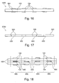
- Figure 16, Figure 17 and Figure 18 show cross-sectional views of structures obtained during carrying out a method of manufacturing a plurality of connector devices 600 in a batch procedure based on panels which are fixed to one another and then separated into sections according to an exemplary embodiment of the invention.
- two printed circuit boards 1600 (such as PCB panels) are provided, one of which being shown in Figure 16 .
- a plurality of connector devices 600 are then manufactured in a simultaneous rather than sequential procedure based on these printed circuit boards 1600.
- Electrically conductive layers deposited on both opposing main surfaces of the printed circuit boards 1600 may be patterned, if desired or required, so as to form individual electrically conductive islands or sections constituting electrically conductive structures 104 of the connector devices 600 to be manufactured.
- a plurality of plug recesses 400 are formed in a spacer board 1700 or panel.
- the spacer board 1700 can be a sheet of electrically insulating material, for instance prepreg, which can be punched or laser processed or milled, etc. in a batch procedure to form the plug recesses 400.
- the spacer board 1700 is arranged between the two printed circuit boards 1600 for forming a board stack. These three boards of the board stack are then fixed to one another, for example by adhering them together.
- connector devices 600 By manufacturing the connector devices 600 according to a batch procedure as illustrated in Figure 16 to Figure 18 , rapid and cheap mass manufacture of connector devices 600 is possible on an industrial scale. If desired, embedded components 106 may be foreseen in one or both of the electrically insulating cores 102 of the printed circuit boards 1600 shown in Figure 16 to extend the electronic functionality of the manufactured connector devices 600.
- any desired number of plug recesses 400 i.e. no, one, two or more plug recesses 400
- any desired number of embedded components 106 i.e. no, one, two or more embedded components 106
- the number of used printed circuit board elements 100 is variable, i.e. may be one, two or more.
- the number of used spacer structure 300 is variable, i.e. may be zero, one, two or more.
- any particular stacking of the mentioned or other components is possible.
- the PCB-based connector device architecture according to exemplary embodiments is highly appropriate for a three-dimensional integration.
- the connector devices 600 may be embodied as male connector pieces, or female connector pieces.
Landscapes
- Engineering & Computer Science (AREA)
- Microelectronics & Electronic Packaging (AREA)
- Combinations Of Printed Boards (AREA)
- Coupling Device And Connection With Printed Circuit (AREA)
Abstract
Description
- The invention relates to a connector device for connection with a counter piece for establishing a mechanical and electric connection.
- Moreover, the invention relates to a connection arrangement.
- Beyond this, the invention relates to a method of manufacturing a connector device.
- Standard connectors generally constitute of metal inserts (i.e. contacts) surrounded by a polymer. Such an assembly is often created during a moulding process (such as injection moulding, transfer moulding, etc.). This method allows the creation of complex mechanical shapes, with a variety of physical properties depending on the selected material combination.
-
US 5,374,196 andUS 5,515,604 disclose laminated connectors which comprise a plurality of layers of rigid dielectric material which are laminated together. The dielectric contains traces which are joined to contact pads, connecting the traces to adjacent circuit boards. Alternatively, the rigid dielectric layers contain recesses where the contact pads are placed. Cross-traces can be placed on each individual layer of dielectric or vias made through the dielectric layers, to interconnect traces. - However, there is still a need for a connector device which can be manufactured in a simple way and connected in a reliable way while offering the flexibility to implement a wide range of electric functions within the connector device.
- It is an object of the invention to provide a simply manufacturable and reliably connectable connector device offering a high flexibility in terms of implementable functions.
- In order to achieve the object defined above, a connector device for connection with a counter piece for establishing a mechanical and electric connection, a connection arrangement, and a method of manufacturing a connector device according to the independent claims are provided.
- According to an exemplary embodiment of the invention, a connector device for connection with a counter piece for establishing a mechanical and electric connection is provided, wherein the connector device comprises at least two printed circuit board (PCB) elements or sections each comprising an electrically insulating core and at least one comprising an electrically conductive structure at least partially on the respective electrically insulating core, wherein the at least one electrically conductive structure is arranged at least partially on an exposed surface of the connector device and is configured for establishing the electric connection with the counter piece upon establishing the mechanical connection with the counter piece.
- According to another exemplary embodiment of the invention, a connection arrangement is provided, wherein the connection arrangement comprises a connector device having the above mentioned features for connection with a counter piece, and the counter piece being configured for being mechanically and electrically connected with the connector device upon plugging the counter piece and the connector device together.
- According to still another exemplary embodiment of the invention, a method of manufacturing a connector device for connection with a counter piece for establishing a mechanical and electric connection is provided, wherein the method comprises forming at least one printed circuit board (PCB) element as a subsection of a printed circuit board (PCB) and comprising an electrically insulating core and an electrically conductive structure at least partially on the electrically insulating core, arranging at least part of the electrically conductive structure on an exposed surface (of the connector device to be manufactured), and configuring the electrically conductive structure for establishing the electric connection with the counter piece upon establishing the mechanical connection between the connector device and the counter piece.
- In the context of the present application, a "printed circuit board" (PCB) may denote a board of an electrically insulting core covered with electrically conductive material and conventionally serving for mounting thereon electronic members (such as packaged electronic chips, sockets, etc.) to be electrically coupled by the electrically conductive material. More specifically, a PCB may mechanically support and electrically connect electronic components using conductive tracks, pads and other features etched from copper sheets laminated onto an electrically non-conductive substrate. PCBs can be single sided (one copper layer), double sided (two copper layers) or of multi-layer type. Conductors on different layers may be connected with plated-through holes called vias. Advanced PCBs may contain components, such as capacitors, resistors or active devices, embedded in the substrate. The term "printed circuit board" may in particular encompass rigid PCBs, flexible PCBs, semiflexible PCBs and/or rigid-flex PCBs.
- In the context of the present application, a "printed circuit board element" may particularly denote a subsection of a PCB, for instance obtained by a singulation of a PCB into multiple printed circuit board elements.
- According to an exemplary embodiment, one or more PCB elements, in particular subsections of a printed circuit board (PCB), are used as main components (or only components) of a connector device. Upon connecting the connector device with a counter piece mechanically by a mutual engagement, an electric connection may be automatically established between electrically conductive structures of the connector device and electrically conductive structures of the counter piece without taking any further action. In other words, the electrically conductive structures of connector device and of the counter piece are automatically aligned in the correct manner by completing the mechanical connection. Forming connector devices based on PCB technology does not only allow to manufacture the connector device with a very simple manufacturing procedure, but also shows a high quality electric coupling safety.
- In the following, further exemplary embodiments of the connector device, the connection arrangement, and the method will be explained.
- In an embodiment, the printed circuit board element is embodied as a section of a printed circuit board. A printed circuit board may hence be separated, for instance by cutting or sawing, into a plurality of sections (for instance at least ten, in particular at least one hundred sections) each constituting a printed circuit board element. Each printed circuit board element may have a rectangular shape. This allows to use a standard material, i.e. PCB, as a basis for the formation of the connector device. Furthermore, standard procedures of PCB technology may be advantageously used.
- In an embodiment, the length dimension and/or the width dimension of the printed circuit board element may be at least three times, in particular at least five times, of a thickness of the printed circuit board element. Thus, a flat and hence very compact connector device may be obtained. The thickness of a printed circuit board element may for instance be in a range between 30 µm and 3 mm, in particular in a range between 1 mm and 2 mm. The length and/or the width of a printed circuit board element may for instance be in a range between 3 mm and 10 cm, in particular in a range between 8 mm and 5 cm.
- In an embodiment, the electrically insulating core comprises or consists of resin. This resin may for instance be an epoxy-based resin or low-CTE (coefficient of thermal expansion) resin, or high-Tg (glass transition temperature) resin.
- In an embodiment, the electrically insulating core may be a planar sheet or plate. For instance, the electrically insulating core may have a thickness in a range between 30µm and 10 cm. A planar shape of the electrically insulating core and of the printed circuit board element may simplify stacking of the printed circuit board element with at least one further printed circuit board element and/or a spacer structure (the latter may comprise one or more plug recesses, as described below).
- In an embodiment, the respective electrically conductive structure comprises at least one patterned electrically conductive layer formed on one at least one of two opposing main surfaces of the electrically insulating core. Such an electrically conductive structure may be made of copper. The electrically conductive material may be deposited on the electrically insulating core, and may be subsequently patterned by a lithography and etching procedure.
- In an embodiment, the electrically conductive structure comprises at least one via extending vertically through the electrically insulating core for electrically connecting the two opposing main surfaces of the electrically insulating core. Each via may be a through hole filled with electrically conductive material such as copper and may be electrically coupled with planar portions of the electrically conductive structure on at least one of the main surfaces of the electrically insulating core.
- In an embodiment, the device comprises at least one embedded component (such as an electronic chip) embedded within the electrically insulating core and electrically coupled to the electrically conductive structure. In other words, at least one electric component may be integrated within the electrically insulating core of the printed circuit board element. This may allow to implement even complex electronic functionalities in a compact connector device. In other words, the connector device may either simply provide an electric connecting function electrically coupling the connector device to the counter piece, or may alternatively provide additional electronic functions.
- Examples of the embedded components are a data storage memory such as a DRAM (or any other memory), a filter (which may for instance be configured as a high pass filter, a low pass filter or a bandpass filter, and which may for instance serve for frequency filtering), an integrated circuit (such as a logic IC), a signal processing component (such as a microprocessor), a power management component, an optical electrically interfacing member (for instance an optoelectronic member), a voltage converter (such as a DC/DC converter or an AC/DC converter), a cryptographic component, a capacitor, an inductance, a switch (for instance a transistor-based switch) and a combination of these and other functional electronic members.
- In an embodiment, at least two printed circuit board elements are vertically stacked so that main surfaces of the at least two printed circuit board elements are arranged in parallel to one another. Thus, the connector architecture according to an exemplary embodiment is compatible with a threedimensional integration, thereby allowing to implement a large number of electronic functions in a small volume.
- In an embodiment, the device further comprises at least one plug recess (which may be a blind hole or a through hole in the device and may be externally accessible) for establishing the mechanical connection with the counter piece. In the context of the present application, a "plug recess" may particularly denote a blind hole or an indentation in the connector device which is externally accessible to serve as a female connector recess configured for receiving a male connector protrusion of the counter piece. For connecting such a connector device mechanically and electrically to the counter piece (such as another connector device) one or more plug recesses may be formed in the PCB element-based connector device mating with correspondingly/inverse shaped protrusions of the counter piece. Hence, the provision of one or more plug recesses renders the connection action performed by a user intuitive, simple, and failure-robust by allowing for a connection only upon connecting mating pairs of connector device and counter piece in terms of size, type and orientation.
- In an embodiment, at least one plug recess is formed exclusively within one of the at least one printed circuit board element. Thus, a single printed circuit board element may be converted into a connector device merely by forming a recess within a single circuit board element to provide for a form closure connection with a counter piece. This results in an extremely compact and simple geometry.
- In an embodiment, at least one plug recess is formed at an interface between two adjacent printed circuit board elements. Such a connector device may be formed by removing material from a first printed circuit board element and by attaching the so processed first printed circuit element to a second printed circuit board element. Consequently, the plug recess is formed directly at an interface between the two printed circuit board elements and is circumferentially delimited by both of them.
- In another embodiment, the device comprises at least two printed circuit board elements and a spacer structure (spacing the printed circuit board elements) is arranged between the at least two printed circuit board elements, wherein at least one plug recess is formed in the spacer structure. In this embodiment, two conventional printed circuit board elements may be taken as such, and a spacer structure may be sandwiched between them for forming the connector device. When forming a recess in the spacer structure, the attachment of the spacer structure between the two printed circuit board elements forms the plug recess circumferentially delimited by one or both printed circuit board elements and the spacer structure. Alternatively, the recess may be formed in an interior of the spacer structure so that the spacer structure alone forms the plug recess.
- For example, the spacer structure may be made of no-flow prepreg material so that fixing the spacer structure between the two printed circuit board elements by pressure and/or thermal energy will start polymerization of the prepreg material without loss of its shape, thereby maintaining a plug recess with a well-defined shape and position within the connector device but exposed to the environment. More generally, the spacer structure may be made of a material which is configured to remain dimensionally stable when fixing the spacer structure between the two printed circuit board elements, in particular by heating and/or applying pressure.
- In an embodiment, the device comprises (additionally or alternatively to the provision of a plug recess) at least one plug protrusion contributing to establishing the mechanical connection with the counter piece. The plug protrusion can be considered as the inverse of a plug recess and can represent a male portion of the connector device cooperating with a correspondingly shaped plug recess of the counter piece.
- In an embodiment, the device comprises at least two printed circuit board elements connected to one another directly, or indirectly via the spacer structure. By forming the connector device from a plurality of printed circuit board elements stacked vertically on top of one another, a three-dimensional integration to fulfil complex connection tasks and also advanced electronic functional tasks may be achieved.
- In an embodiment, at least part of the electrically conductive structure is arranged on an exposed surface of the at least one printed circuit board element. Since printed circuit board elements may already comprise electrically conductive structures such as traces of copper, they can be used in the PCB-based connector device for providing the electronic connection tasks.
- In an embodiment, at least part of the electrically conductive structure is arranged on at least one of two opposing main surfaces of the at least one printed circuit board element. In another embodiment, at least part of the electrically conductive structure is arranged on at least one of side walls perpendicular to two opposing main surfaces of the at least one printed circuit board element. In still another embodiment, at least part of the electrically conductive structure is arranged on an exposed surface of the plug recess, in particular parallel and/or perpendicular to two opposing main surfaces of the printed circuit board element(s). Therefore, the PCB based architecture of forming connector devices is compatible with very different orientations of the electrically conductive structure in a horizontal and/or vertical direction. The electrically conductive structure may be arranged at one, two, three, four or even more exposed surfaces of the device, depending on the electric contacting tasks required for a specific application.
- In an embodiment, each of the at least two printed circuit board elements is formed as a subsection of a printed circuit board. In particular, a printed circuit board may be used as a semifinished product and may be singularized into a large number of printed circuit board elements, and the latter may in tum be used for manufacturing the connector device.
- In an embodiment, the device is configured as one of the group consisting of a Lightning® connector (i.e. a connector having eight pins), a MIPI (Mobile Industry Processor Interface) connector, a USB (Universal Serial Bus) connector, a HDMI (High Definition Multimedia Interface), and a ZIF (Zero Insertion Force) connector. Connector devices according to these and many other connector standards can be formed on the basis of PCB elements.
- In an embodiment, the counter piece is configured as a connector device having the above mentioned features. Hence, in such an embodiment, both connector pieces of the connection arrangement can be constructed based on PCB technology. This results in a very compact design and allows to be manufactured with low cost.
- In an embodiment, the plug recess is formed by mechanically removing material of the at least one printed circuit board element and/or a spacer structure arranged between two printed circuit board elements, in particular by one of the group consisting of milling, laser processing, cutting, and punching. Such a mechanical procedure is simpler, faster and cheaper than for instance a chemical removal procedure (which may be implemented according to other embodiments as well). Furthermore, a mechanical removal of material involves less waste and pollution.
- In an embodiment, the spacer structure having one or more plug recesses is connected between the two printed circuit board elements by adhering and/or pressing. For instance, an adhesive may be used which starts adhering upon application of thermal energy. Alternatively, an adhesive may be used which starts adhering upon applying pressure. The adhesive material may be separate from the printed circuit board element(s) and/or the spacer structure. Alternatively, the adhesive material may form part of the printed circuit board element(s) and/or the spacer structure. The latter alternative is particularly advantageous since it keeps the number of components used for the manufacturing procedure small and hence the manufacturing procedure simple.
- In an embodiment, the method comprises providing at least one printed circuit board (in particular a full PCB), optionally patterning electrically conductive material on at least one main surface of the at least one printed circuit board, and singularising the at least one printed circuit board with its electrically conductive material (and optionally plug recesses) into a plurality of sections, each section constituting a connector device according to an exemplary embodiment. Therefore, at least a part of the manufacture of the connector device may be formed in a batch process, i.e. for a plurality of connector devices simultaneously, based on the processing of one or more boards which is/are then singularized, for instance by sawing, laser cutting, or etching. This allows to manufacture the connector devices in a fast time and with low cost.
- In an embodiment, the method further comprises forming a plurality of plug recesses (in at least one printed circuit board and/or a spacer structure) before the singularising. Thus, also the formation of the plug recesses may be performed on board level, i.e. during a batch process.
- In an embodiment, the method further comprises stacking at least two printed circuit boards before singularizing the stack into the plurality of sections (constituting connector devices). Therefore, the concept of forming connector devices on the basis of PCB technologies allows a three-dimensional integration.
- In an embodiment, the method comprises arranging a spacer board (such as an electrically insulating sheet) between the at least two stacked printed circuit boards before singularizing the stack into the plurality of sections each of which comprising a portion of the spacer board constituting a spacer structure. Thus, also the provision of a spacer board having a plurality of plug recesses can be integrated in the batch process of manufacturing multiple connector devices simultaneously.
- In one embodiment, the connector device may be a standalone device. Thus, the connector device may be a body which may be handled separately from other apparatuses and may be selectively plugged onto or into another apparatus. For example, such a connector device may be a portable memory stick.
- In another embodiment, the connector device may form part of a large apparatus. For instance, it may be connected via a cable or directly to an apparatus such as a computer for connecting the apparatus to a partner device or counter piece.
- The aspects defined above and further aspects of the invention are apparent from the examples of embodiment to be described hereinafter and are explained with reference to these examples of embodiment.
- The invention will be described in more detail hereinafter with reference to examples of embodiment but to which the invention is not limited.
-
Figure 1 and Figure 2 illustrate cross sections of printed circuit board elements used as a basis for manufacturing a connector device according to an exemplary embodiment of the invention. -
Figure 3 illustrates a side view and a plan view of a spacer structure used as a basis for manufacturing a connector device according to an exemplary embodiment of the invention in connection with the printed circuit board elements ofFigure 1 and/orFigure 2 . -
Figure 4 illustrates a plan view of the spacer structure ofFigure 3 after having formed a plug recess in the spacer structure by a purely mechanical material removal procedure. -
Figure 5 illustrates a structure obtained during carrying out a procedure of assembling two printed circuit board elements as shown inFigure 2 with a plug recess comprising spacer structure as shown inFigure 4 for manufacturing a connector device according to an exemplary embodiment of the invention. -
Figure 6 shows a cross-sectional view of a connector device according to an exemplary embodiment of the invention manufactured according to the procedure ofFigure 2 to Figure 5 . -
Figure 7 illustrates a structure obtained during carrying out a procedure of assembling two printed circuit board elements as shown inFigure 1 and Figure 2 with a plug recess comprising spacer structure as shown inFigure 4 for manufacturing a connector device according to another exemplary embodiment of the invention. -
Figure 8 shows a cross-sectional view of a connector device according to an exemplary embodiment of the invention manufactured according to the procedure ofFigure 1 to Figure 4 andFigure 7 . -
Figure 9 illustrates a structure obtained during carrying out a procedure of assembling two printed circuit board elements as shown inFigure 1 with a plug recess comprising spacer structure as shown inFigure 4 for manufacturing a connector device according to still another exemplary embodiment of the invention. -
Figure 10 shows a cross-sectional view of a connector device according to an exemplary embodiment of the invention manufactured according to the procedure ofFigure 1 ,Figure 3 to Figure 4 andFigure 9 . -
Figure 11 and Figure 12 show three-dimensional views of connector devices according to exemplary embodiments of the invention. -
Figure 13 shows a cross-sectional view of a connector device according to an exemplary embodiment of the invention manufactured by directly connecting two printed circuit board elements to one another, one of which comprising a plug recess. -
Figure 14 shows a cross-sectional view of a connector device according to an exemplary embodiment of the invention manufactured on the basis of a single printed circuit board element comprising a plug recess in its interior. -
Figure 15 shows a connection arrangement formed by two correspondingly configured connector devices to be connected electrically and mechanically according to an exemplary embodiment of the invention. -
Figure 16 to Figure 18 show cross-sectional views of structures obtained during carrying out a method of manufacturing a plurality of connector devices in a batch procedure according to an exemplary embodiment of the invention. - The illustrations in the drawings are schematical. In different drawings, similar or identical elements are provided with the same reference signs.
- Before, referring to the drawings, exemplary embodiments will be described in further detail, some basic considerations will be summarized based on which exemplary embodiments of the invention have been developed.
- An embodiment of the invention provides a PCB-based connector device. Exemplary embodiments may have a simple mechanical shape (such as rectangles/squares and combinations thereof) and interconnection patterns. Advantages of such a connector architecture are, inter alia, the following:
- No need for tooling, thus very-low set-up cost and time,
- Capability for large-scale manufacturing thanks to panel-level/board level or batch processing,
- Capability for very-complex routing thanks to the opportunity to implement a multi-layer architecture,
- Capability for very-fine contact surfaces thanks to the possibility of fine-line structuring,
- Capability for integrated functions thanks to an optional embedding of embedded components (such as discrete components or integrated layers).
- In an embodiment of the manufacturing procedure, contacts may be created through standard structuring (such as tracks, edge-plating and/or plated through holes depending on the end-orientation). After that, panels may be stacked and bonded to achieve the desired architecture. Solder paste can then be placed in specific areas to improve soldering behaviour. To finish the product, the connector devices may be singulated from the panel.
- One task which may be solved by exemplary embodiments of the invention is to create the conducting surface(s) in one or multiple directions, in order to meet integration demands. Three exemplary possible solutions are:
- Standard PCB tracks
- Vertical plating
- Plated through holes (optionally sawn)
- By applying one or more of these three processes, contact surfaces and soldering surfaces can be created at desired angles (such as 90°/180°) of each other. One such combination, involves "Standard PCB Tracks" and "Sawn plated through holes".
- Exemplary embodiments allow the creation of complex geometrical shapes, the separation of the connector device from the PCB for increased placement flexibility and the addition of functions through embedding. This may be achieved by increasing the mechanical complexity and the functionalities. Those functions can include:
- Signal processing,
- Power management,
- DRM,
- Opto-electrical interfacing.
- Due to the flexibility of PCB manufacturing processes, shapes can be repeatedly stacked, thereby dramatically increasing the number of contact surfaces (for instance four contact surfaces, or even significantly more contact surfaces).
-
Figure 1 and Figure 2 illustrate cross sections of printed circuit board elements 100 (which may be subsections of larger printed circuit boards/panels, compare for instanceFigure 16 ) used as a basis for manufacturing a connector device 600 (compare for instanceFigure 6 ) according to an exemplary embodiment of the invention. - The printed
circuit board elements 100 ofFigure 1 comprise an electrically insulatingcore 102 which is made of a (for instance) reinforced epoxy-based resin (or prepreg) material and is shaped as a plate or sheet. Both opposing main surfaces of the electrically insulatingcore 102 are covered with planar sections of an electricallyconductive structure 104 embodied as respectively patterned electrically conductive layers formed on each of two opposing main surfaces of the electrically insulatingcore 102 In a horizontal direction according toFigure 1 . The electricallyconductive structure 104 furthermore comprises vias extending, according toFigure 1 vertically, through the electrically insulatingcore 102 for electrically connecting the two opposing main surfaces of the electrically insulatingcore 102. Therefore, the portions of the electricallyconductive structure 104 on the two opposing main surfaces of the electrically insulatingcore 102 are electrically coupled by a short path by via the vias. In view of the foregoing, the electricallyconductive structure 104 is partially arranged on an exposed surface of the printedcircuit board element 100, and is partly arranged in an interior of the printedcircuit board element 100. Thus, the available volume can be very efficiently used to provide a complex circuitry. - An embedded
component 106 is integrated or embedded within the electrically insulatingcore 102 and is electrically coupled to the planar portions of the electricallyconductive structure 104 on the two opposing main surfaces of the electrically insulatingcore 102 by means of part of the vias. - The embedded
component 106 may be any desired type of active electric component or passive electric component. In the shown embodiment, the embeddedcomponent 106 may be embodied as a semiconductor memory such as a DRAM in order to extend the electric connection functionality of theconnector device 600 to be manufactured by providing a data storage function. Hence, anintelligent connector device 600 with extended electronic functionality may be formed when implementing the embeddedcomponent 106 into the printedcircuit board element 100. - Although not shown in
Figure 1 , it is also possible in this and other embodiments described herein that, additionally or alternatively, one or more lateral side surfaces (i.e. vertical surface portions according toFigure 1 ) of the printedcircuit board element 100 is/are covered with electrically conductive material such as copper to form the electricallyconductive structure 104. - The printed
circuit board element 100 shown inFigure 2 , which may form the basis ofconnector devices 600 manufactured according to other exemplary embodiments differs from the printedcircuit board element 100 shown inFigure 1 in that the embeddedcomponent 106 and vias connecting the embeddedcomponent 106 and forming part of the electricallyconductive structure 104 are omitted. Thus, the functionality of aconnector device 600 according to an embodiment using only printedcircuit board elements 100 ofFigure 2 as a basis may exclusively provide a desired electric coupling scheme between individual ones of pads of the electricallyconductive structure 104 and other pads of the corresponding counter piece physically contacting the pads of the electricallyconductive structure 104. -
Figure 3 illustrates a side view and a plan view of a sheet-like spacer structure 300 used as a basis for manufacturingconnector devices 600 according to exemplary embodiments of the invention in connection with the printedcircuit board elements 100 ofFigure 1 and/orFigure 2 . - The
spacer structure 300 can also be formed of a glass fiber reinforced epoxy-based resin (or prepreg) material and is shaped as a plate or sheet. It is preferable that thespacer structure 300 is made of a material which does not change its shape (for instance does not start to flow) upon applying thermal energy and/or pressure for adhering thespacer structure 300 between two printedcircuit board elements 100, as shown inFigure 1 or Figure 2 , because this ensures the maintenance of the correct orientation of the material of the spacer structure 300 (and therefore the task of spacing two printed circuit board elements 100) when forming aconnector device 600. For example, this may be guaranteed by embodying thespacer structure 300 from a no flow prepreg material. -
Figure 4 illustrates a plan view of thespacer structure 300 ofFigure 3 after having formed aplug recess 400 in thespacer structure 300 by a purely mechanical material removal procedure. - Although a chemical material removal procedure (such as etching) is generally possible as well, it is nevertheless preferred to apply a mechanical removal procedure (such as milling, cutting or punching) or laser removal process because this allows the formation of a precisely shaped and dimensioned
plug recess 400 in a very simple way. As can be taken fromFigure 4 , thespacer structure 300 remains a continuous body after formation of theplug recess 400 which therefore does not separate thespacer structure 300 into isolated islands. This allows to simplify the handling of the recessedspacer structure 300 for manufacturing aconnector device 600, because, when taking this measure, only one piece has to be handled and sandwiched between two printedcircuit board elements 100. After formation of theplug recess 400, thespacer structure 300 shown inFigure 4 is basically U-shaped, and theplug recess 400 has a rectangular cross-section. -
Figure 5 illustrates a structure obtained during carrying out a procedure of assembling two printedcircuit board elements 100 as shown inFigure 2 with aplug recess 400 comprisingspacer structure 300 as shown inFigure 4 for manufacturing aconnector device 600 according to an exemplary embodiment of the invention. As shown inFigure 5 , one printedcircuit board element 100, onespacer structure 300 and another printedcircuit board element 100 are aligned on top of each other to form a vertical stack of planar bodies. The side edges of the stacked bodies coincide or match to one another and are in alignment (with the exception of the plug recess 400). Thus, acompact connector device 600 may be obtained. - After having aligned the printed
circuit board elements 100 and thespacer structure 300 as shown inFigure 5 , they are connected to one another by the application of pressure and/or thermal energy (i.e. by an increase of the temperature). For instance, prepreg material of thespacer structure 300 and/or the electrically insulatingcore 102 of the printedcircuit board elements 100 may become soft or may start melting at a certain temperature of for instance 90°C, so that polymerization starts and curing or hardening of the material begins. Therefore, the printedcircuit board elements 100 with the sandwiched spacer structure 360 are laminated together, wherein this procedure maintains the physical dimensions of thespacer structure 300 including itsplug recess 400 unchanged. Hence, arobust connector device 600 with precisely definable dimensions is obtained. This is of upmost advantage, because theconnector device 600 and its counter piece can only be brought in mechanical and electrical connection by plugging them together when the mechanical connection elements (i.e. theplug recess 400 of theconnector device 600 and an inversely shaped protrusion of the counter piece, not shown) are configured to match with form closure and when the electrical connection elements (i.e. the pads constituted by the exposed sections of the electricallyconductive structure 104 and corresponding pads of the counter piece, not shown) remain located at accurately definable positions. -
Figure 6 shows a cross-sectional view of theconnector device 600 in a PCB-only-combination (i.e. without embedded component 106) according to an exemplary embodiment of the invention manufactured according to the procedure ofFigure 2 to Figure 5 . - The PCB-based
connector device 600 is configured for being electrically coupled with a counter piece (not shown inFigure 6 ) for establishing a defined mechanical and electric connection. Theconnector device 600 comprises the two printedcircuit board elements 100 with their insulatingcores 102 and electricallyconductive structures 104 partially on and partially in the electrically insulatingcore 102. Vertically stacked between the two printedcircuit board elements 100 is thespacer structure 300 with itsplug recess 400 for establishing the mechanical connection with thecounter piece 1500. As can be taken fromFigure 6 , various sections or pads of the electricallyconductive structures 104 are arranged on exposed surfaces of theconnector device 600 and are configured for establishing the electric connection with the counter piece upon establishing the mechanical connection with the counter piece. - Various exposed sections of the electrically
conductive structure 104 are arranged on an exposed surface of theplug recess 400, according toFigure 6 all parallel to the two opposing main surfaces of the printedcircuit board elements 100 and thespacer structure 300. With a corresponding dimensioning, adaptation of the shape of theplug recess 400 and the arrangement of the pads realized by the electricallyconductive structures 104, thedevice 600 may be configured as a specific type of connector (for instance a MIPI connector). -
Figure 7 illustrates a structure obtained during carrying out a procedure of assembling two printedcircuit board elements 100 as shown inFigure 1 and Figure 2 with aplug recess 400 comprisingspacer structure 300 as shown inFigure 4 for manufacturing aconnector device 600 according to another exemplary embodiment of the invention. - The arrangement shown in
Figure 7 differs from the arrangement shown inFigure 5 in that the lower printedcircuit board element 100 now comprises an embeddedcomponent 106, i.e. is configured as a printedcircuit board element 100 shown inFigure 1 . By applying a connection procedure as described above referring toFigure 6 , the arrangement shown inFigure 7 can be transformed into theconnector device 600 shown inFigure 8 . -
Figure 8 shows a cross-sectional view of the PCB-embedded-combination connector device 600 according to an exemplary embodiment of the invention manufactured according to the procedure ofFigure 1 to Figure 4 andFigure 7 . - When the embedded
component 106 is configured as a semiconductor memory such as a DRAM, theconnector device 600 ofFigure 8 can serve as a portable memory-connector-arrangement, such as a PCB-based USB stick. For example, with a corresponding dimensioning, adaptation of the shape of theplug recess 400 and the arrangement of the pads realized by the electricallyconductive structures 104, thesmart connector device 600 may be configured as a connector of a specific type (for instance a USB connector) with data storage function. -
Figure 9 illustrates a structure obtained during carrying out a procedure of assembling two printedcircuit board elements 100 as shown inFigure 1 with aplug recess 400 comprisingspacer structure 300 as shown inFigure 4 for manufacturing aconnector device 600 according to still another exemplary embodiment of the invention. - The arrangement shown in
Figure 9 differs from the arrangement shown inFigure 7 in that now also the upper printedcircuit board element 100 comprises an embeddedcomponent 106, i.e. is configured as a printedcircuit board element 100 shown inFigure 1 . By applying a connection procedure as described above referring toFigure 6 , the arrangement shown inFigure 9 can be transformed into theconnector device 600 shown inFigure 10 . -
Figure 10 shows a cross-sectional view of aconnector device 600 according to an exemplary embodiment of the invention manufactured according to the procedure ofFigure 1 ,Figure 3 to Figure 4 andFigure 9 . - The function of the
connector device 600 shown inFigure 10 depends on the configuration of the embeddedcomponents 106. For instance, one of the embeddedcomponents 106 may provide an encryption function, the other one a voltage converter function, etc. Thus, basically any desired electrical function and functional combination may be integrated in thecompact connector device 600. -
Figure 11 and Figure 12 show three-dimensional views ofconnector devices 600 according to exemplary embodiments of the invention. - According to the
connector device 600 shown inFigure 11 (which may be formed based on one or more printed circuit board elements 100), part of the electricallyconductive structure 104 is arranged on vertical side walls within theplug recess 400 perpendicular to two horizontal opposing main surfaces of the printedcircuit board element 100, and another part of the electricallyconductive structure 104 is arranged horizontally on and parallel to horizontal opposing main surfaces of the printedcircuit board element 100. - According to the
connector device 600 shown inFigure 12 , all sections of the electricallyconductive structure 104 are arranged on vertical side walls within theplug recess 400 and outside of theplug recess 400 perpendicular to two horizontal opposing main surfaces of the printed circuit board element(s) 100. -
Figure 13 shows a cross-sectional view of aconnector device 600 according to an exemplary embodiment of the invention manufactured by connecting two printedcircuit board elements 100 to one another, one of which comprising aplug recess 400. - According to the
connector device 600 shown inFigure 13 , theplug recess 400 is formed at an interface between two adjacent printedcircuit board elements 100. Thedevice 600 hence comprises two printedcircuit board elements 100 connected to one another directly. In this embodiment, theplug recess 400 is formed by removing material from one of the printedcircuit board elements 100 rather than providing aseparate spacer structure 300. Hence, aspacer structure 300 is omitted according toFigure 13 , and theentire connection device 600 is formed exclusively from two printedcircuit board elements 100. -
Figure 14 shows a cross-sectional view of aconnector device 600 according to an exemplary embodiment of the invention manufactured on the basis of a single printedcircuit board element 100 comprising aplug recess 400 in its interior. - According to
Figure 14 , theplug recess 400 is formed exclusively within exactly one printedcircuit board element 100. In other words, theplug recess 400 is formed by removing material from the single printedcircuit board element 100. Hence, aspacer structure 300 as well as further printedcircuit board elements 100 are omitted according toFigure 13 , and theentire connection device 600 is formed exclusively from one printedcircuit board element 100. -
Figure 15 shows aconnection arrangement 1550 formed by two correspondingly configuredconnector devices 600 to be connected electrically and mechanically according to an exemplary embodiment of the invention. - The
connection arrangement 1550 comprises aconnector device 600 of the type described above for connection with thecounter piece 1500. Thecounter piece 1500 is configured for being mechanically and electrically connected with theconnector device 600 upon plugging thecounter piece 1500 in theplug recess 400. Thecounter piece 1500 is also configured as a PCB-based connector device of the type described above (but may, in other embodiments, be manufactured in other way, for instance according to another connector technology or as a corresponding part, such as a plug or a socket, of an electronic apparatus, such as a computer). - Along a vertical direction of
Figure 15 , both theconnector device 600 and thecounter piece 1500 comprise alternating sequences of plug recesses 400 and plugprotrusions 1502. These sequences are adapted to match and align to one another so that theconnector device 600 and thecounter piece 1500 may be plugged together by approaching them along a horizontal direction ofFigure 15 for an engagement thereof. By this engagement, both a mechanical and electrical connection is established, since the respective sections of the electricallyconductive structures 104 are then brought in direct physical contact with one another. -
Figure 16, Figure 17 and Figure 18 show cross-sectional views of structures obtained during carrying out a method of manufacturing a plurality ofconnector devices 600 in a batch procedure based on panels which are fixed to one another and then separated into sections according to an exemplary embodiment of the invention. - In the framework of this manufacturing method, two printed circuit boards 1600 (such as PCB panels) are provided, one of which being shown in
Figure 16 . A plurality ofconnector devices 600 are then manufactured in a simultaneous rather than sequential procedure based on these printedcircuit boards 1600. Electrically conductive layers deposited on both opposing main surfaces of the printedcircuit boards 1600 may be patterned, if desired or required, so as to form individual electrically conductive islands or sections constituting electricallyconductive structures 104 of theconnector devices 600 to be manufactured. - As can be taken from
Figure 17 , a plurality of plug recesses 400 are formed in aspacer board 1700 or panel. Thespacer board 1700 can be a sheet of electrically insulating material, for instance prepreg, which can be punched or laser processed or milled, etc. in a batch procedure to form the plug recesses 400. - As can be taken from
Figure 18 , thespacer board 1700 is arranged between the two printedcircuit boards 1600 for forming a board stack. These three boards of the board stack are then fixed to one another, for example by adhering them together. - As indicated schematically by vertical dotted lines in
Figure 18 , it is then possible to singularize the integral board stack into a plurality of sections, each section constituting aconnector device 600. - By manufacturing the
connector devices 600 according to a batch procedure as illustrated inFigure 16 to Figure 18 , rapid and cheap mass manufacture ofconnector devices 600 is possible on an industrial scale. If desired, embeddedcomponents 106 may be foreseen in one or both of the electrically insulatingcores 102 of the printedcircuit boards 1600 shown inFigure 16 to extend the electronic functionality of the manufacturedconnector devices 600. - Referring to the embodiments described above, it should of course be mentioned that any desired number of plug recesses 400 (i.e. no, one, two or more plug recesses 400) and/or any desired number of embedded components 106 (i.e. no, one, two or more embedded components 106) may be implemented. Also, the number of used printed
circuit board elements 100 is variable, i.e. may be one, two or more. Beyond this, the number of usedspacer structure 300 is variable, i.e. may be zero, one, two or more. In particular, any particular stacking of the mentioned or other components is possible. In other words, the PCB-based connector device architecture according to exemplary embodiments is highly appropriate for a three-dimensional integration. Theconnector devices 600 may be embodied as male connector pieces, or female connector pieces. - It should be noted that the term "comprising" does not exclude other elements or steps and the "a" or "an" does not exclude a plurality. Also elements described in association with different embodiments may be combined.
- It should also be noted that reference signs in the claims shall not be construed as limiting the scope of the claims.
- Implementation of the invention is not limited to the preferred embodiments shown in the figures and described above. Instead, a multiplicity of variants are possible which use the solutions shown and the principle according to the invention even in the case of fundamentally different embodiments.
Claims (15)
- A connector device (600) for connection with a counter piece (1500) for establishing a mechanical and electric connection, wherein the connector device (600) comprises:at least two printed circuit board elements (100) each comprising an electrically insulating core (102) and at least one comprising an electrically conductive structure (104) at least partially on the respective electrically insulating core (102);wherein the at least one electrically conductive structure (104) is arranged at least partially on an exposed surface of the connector device (600) and is configured for establishing the electric connection with the counter piece (1500) upon establishing the mechanical connection with the counter piece (1500).
- The device (600) of claim 1, comprising at least one of the following features:at least one of the electrically insulating cores (102) comprises or consists of resin, in particular an epoxy-based resin;at least one of the electrically insulating cores (102) is configured as a plate;the at least one electrically conductive structure (104) comprises at least one patterned electrically conductive layer formed on one at least one of two opposing main surfaces of the respective electrically insulating core (102);the at least one electrically conductive structure (104) comprises at least one via extending through the respective electrically insulating core (102) for electrically connecting the two opposing main surfaces of the respective electrically insulating core (102);the at least two printed circuit board elements (100) are vertically stacked so that main surfaces of the at least two printed circuit board elements (100) are arranged in parallel to one another;the device (600) comprises at least one plug protrusion contributing to establishing the mechanical connection with the counter piece (1500);the at least two printed circuit board elements (100) are connected to one another directly or via the spacer structure (300) indirectly;at least part of the electrically conductive structure (104) is arranged on at least one of two opposing main surfaces of at least one of the printed circuit board elements (100);at least part of the electrically conductive structure (104) is arranged on at least one of side walls perpendicular to two opposing main surfaces of at least one of the printed circuit board elements (100);each of the at least two printed circuit board elements (100) is formed as a subsection of a printed circuit board (1600);the device (600) is configured as one of the group consisting of a Lightning connector, a MIPI connector, a USB connector, a HDMI connector, and a ZIF connector.
- The device (600) of claim 1 or 2, comprising at least one embedded component (106) embedded within the respective electrically insulating core (102) and electrically coupled to the respective electrically conductive structure (104).
- The device (600) of claim 3, wherein the at least one embedded component (106) comprises at least one of the group consisting of an active electric component, and a passive electric component, in particular at least one of the group consisting of a data storage memory, a filter, an integrated circuit, a signal processing component, a power management component, a voltage converter, a cryptographic component, a capacitor, an inductance, and an optical electrically interfacing member.
- The device (600) of any one of claims 1 to 4, further comprising at least one plug recess (400) for establishing the mechanical connection with the counter piece (1500).
- The device (600) of claim 5, comprising at least one of the following features:at least one plug recess (400) is formed exclusively within one of the at least two printed circuit board elements (100);at least one plug recess (400) is formed at an interface between two adjacent ones of the printed circuit board elements (100);the device (600) comprises a spacer structure (300) arranged between the at least two printed circuit board elements (100), wherein at least one plug recess (400) is formed in the spacer structure (300);at least part of the electrically conductive structure (104) is arranged on an exposed surface of the plug recess (400), in particular parallel and/or perpendicular to two opposing main surfaces of at least one of the printed circuit board elements (100).
- A connection arrangement (1550), wherein the connection arrangement (1550) comprises:a connector device (600) of any one of claims 1 to 6 for connection with a counter piece (1500); andthe counter piece (1500) being configured for being mechanically and electrically connected with the connector device (600) upon plugging the counter piece (1500) and the connector device (600) together.
- A method of manufacturing a connector device (600) for connection with a counter piece (1500) for establishing a mechanical and electric connection, wherein the method comprises:forming at least one printed circuit board element (100) as a subsection of a printed circuit board (1600) and comprising an electrically insulating core (102) and an electrically conductive structure (104) at least partially on the electrically insulating core (102);arranging at least part of the electrically conductive structure (104) on an exposed surface and configuring the electrically conductive structure (104) for establishing the electric connection with the counter piece (1500) upon establishing the mechanical connection between the connector device (600) and the counter piece (1500).
- The method of claim 8, wherein the method further comprises forming at least one plug recess (400) for establishing the mechanical connection with the counter piece (1500).
- The method of claim 9, wherein the at least one plug recess (400) is formed by mechanically removing material of the at least one printed circuit board element (100) and/or a spacer structure (300) arranged between two printed circuit board elements (100), in particular by one of the group consisting of milling, laser processing, cutting, and punching.
- The method of claim 9 or 10, wherein a spacer structure (300) having the at least one plug recess (400) is connected between two printed circuit board elements (100) by adhering and/or applying pressure.
- The method of any one of claims 8 to 11, wherein the method comprises:providing at least one printed circuit board (1600);patterning electrically conductive material on at least one main surface of the at least one printed circuit board (1600);singulating the at least one printed circuit board (1600) with the patterned electrically conductive material into a plurality of sections, each section constituting a connector device (600).
- The method of claim 12, wherein the method further comprises forming a plurality of plug recesses (400) before the singulation.
- The method of claim 12 or 13, wherein the method further comprises stacking at least two printed circuit boards (1600) before singulating the stack into the plurality of sections.
- The method of claim 14, further comprising arranging a spacer board (1700) between the at least two stacked printed circuit boards (1600) before singulating the stack into the plurality of sections each of which comprising a portion of the spacer board (1700) constituting a spacer structure (300).
Priority Applications (4)
| Application Number | Priority Date | Filing Date | Title |
|---|---|---|---|
| EP14290041.4A EP2911486B1 (en) | 2014-02-19 | 2014-02-19 | PCB-based connector device |
| PCT/EP2015/053446 WO2015124646A1 (en) | 2014-02-19 | 2015-02-18 | Pcb-based connector device |
| US15/119,839 US10886670B2 (en) | 2014-02-19 | 2015-02-18 | PCB-based connector device |
| CN201580009202.5A CN106165550B (en) | 2014-02-19 | 2015-02-18 | Electrical connector based on PCB |
Applications Claiming Priority (1)
| Application Number | Priority Date | Filing Date | Title |
|---|---|---|---|
| EP14290041.4A EP2911486B1 (en) | 2014-02-19 | 2014-02-19 | PCB-based connector device |
Publications (2)
| Publication Number | Publication Date |
|---|---|
| EP2911486A1 true EP2911486A1 (en) | 2015-08-26 |
| EP2911486B1 EP2911486B1 (en) | 2024-07-31 |
Family
ID=50236121
Family Applications (1)
| Application Number | Title | Priority Date | Filing Date |
|---|---|---|---|
| EP14290041.4A Active EP2911486B1 (en) | 2014-02-19 | 2014-02-19 | PCB-based connector device |
Country Status (4)
| Country | Link |
|---|---|
| US (1) | US10886670B2 (en) |
| EP (1) | EP2911486B1 (en) |
| CN (1) | CN106165550B (en) |
| WO (1) | WO2015124646A1 (en) |
Families Citing this family (8)
| Publication number | Priority date | Publication date | Assignee | Title |
|---|---|---|---|---|
| EP3148300B1 (en) * | 2015-09-24 | 2023-07-26 | AT & S Austria Technologie & Systemtechnik Aktiengesellschaft | Connection system for electronic components |
| US20170196094A1 (en) * | 2015-12-30 | 2017-07-06 | AT&S Austria | Electronic component packaged in a flexible component carrier |
| DE102016213697A1 (en) * | 2016-07-26 | 2018-02-01 | Zf Friedrichshafen Ag | Printed circuit board assembly |
| CN108307581A (en) | 2017-01-12 | 2018-07-20 | 奥特斯奥地利科技与系统技术有限公司 | Electronic equipment with embedded components load-bearing part |
| JP6835971B2 (en) * | 2017-08-04 | 2021-02-24 | 株式会社フジクラ | Manufacturing method of multi-layer printed wiring board and multi-layer printed wiring board |
| US20190387615A1 (en) * | 2018-06-14 | 2019-12-19 | Microsoft Technology Licensing, Llc | Multi-layer interconnected electro-thermal system having a thermally non-expansive support for mounting positionally related sensor components |
| CN115379645A (en) * | 2019-12-19 | 2022-11-22 | Oppo广东移动通信有限公司 | Substrate assembly and network device |
| CN111867255B (en) * | 2020-07-07 | 2021-07-09 | 胜宏科技(惠州)股份有限公司 | Manufacturing method of PCB with horizontally segmented metalized side wall for display screen |
Citations (4)
| Publication number | Priority date | Publication date | Assignee | Title |
|---|---|---|---|---|
| GB357171A (en) * | 1930-06-10 | 1931-09-10 | Paragon Rubber Mfg Company Ltd | Improvements in and relating to wireless and like electrical apparatus |
| US5374196A (en) | 1992-10-07 | 1994-12-20 | Fujitsu Limited | High-density/long-via laminated connector |
| US5515604A (en) | 1992-10-07 | 1996-05-14 | Fujitsu Limited | Methods for making high-density/long-via laminated connectors |
| US20140017940A1 (en) * | 2012-07-11 | 2014-01-16 | Tyco Electronics Corporation | Layered connector and method of manufacturing a layered connector |
Family Cites Families (16)
| Publication number | Priority date | Publication date | Assignee | Title |
|---|---|---|---|---|
| US5219292A (en) * | 1992-04-03 | 1993-06-15 | Motorola, Inc. | Printed circuit board interconnection |
| US6047470A (en) * | 1997-08-20 | 2000-04-11 | Micron Technology, Inc. | Singulation methods |
| TW492114B (en) * | 2000-06-19 | 2002-06-21 | Advantest Corp | Method and apparatus for edge connection between elements of an integrated circuit |
| JP2002280690A (en) | 2001-03-19 | 2002-09-27 | Fuji Photo Film Co Ltd | Printed wiring board and connection structure thereof |
| JP4276881B2 (en) | 2003-04-30 | 2009-06-10 | 日本圧着端子製造株式会社 | Multilayer printed wiring board connection structure |
| US6981878B1 (en) * | 2004-02-07 | 2006-01-03 | Edward Herbert | Connection system for fast power supplies |
| US20060292898A1 (en) * | 2005-06-23 | 2006-12-28 | 3M Innovative Properties Company | Electrical interconnection system |
| TWI336608B (en) * | 2006-01-31 | 2011-01-21 | Sony Corp | Printed circuit board assembly and method of manufacturing the same |
| US20070270040A1 (en) * | 2006-05-05 | 2007-11-22 | Jang Sang J | Chamfered Memory Card |
| TWI324821B (en) * | 2007-02-14 | 2010-05-11 | Advanced Semiconductor Eng | Package structure for connecting i/o module |
| DE102008000842A1 (en) * | 2008-03-27 | 2009-10-01 | Robert Bosch Gmbh | Method for producing an electronic assembly |
| US8708745B2 (en) * | 2011-11-07 | 2014-04-29 | Apple Inc. | Dual orientation electronic connector |
| JP5766593B2 (en) * | 2011-12-09 | 2015-08-19 | 日本特殊陶業株式会社 | Light-emitting element mounting wiring board |
| US8941013B2 (en) * | 2012-05-30 | 2015-01-27 | Shawn X. ARNOLD | Multilayer laminated structure for plug and connector with spring finger interconnecting feature |
| KR20150065029A (en) * | 2013-12-04 | 2015-06-12 | 삼성전기주식회사 | Printed circuit board, manufacturing method thereof and semiconductor package |
| CN105931717B (en) * | 2016-06-08 | 2017-10-03 | 深圳市华星光电技术有限公司 | A kind of flexible flat cable |
-
2014
- 2014-02-19 EP EP14290041.4A patent/EP2911486B1/en active Active
-
2015
- 2015-02-18 CN CN201580009202.5A patent/CN106165550B/en not_active Expired - Fee Related
- 2015-02-18 US US15/119,839 patent/US10886670B2/en not_active Expired - Fee Related
- 2015-02-18 WO PCT/EP2015/053446 patent/WO2015124646A1/en not_active Ceased
Patent Citations (4)
| Publication number | Priority date | Publication date | Assignee | Title |
|---|---|---|---|---|
| GB357171A (en) * | 1930-06-10 | 1931-09-10 | Paragon Rubber Mfg Company Ltd | Improvements in and relating to wireless and like electrical apparatus |
| US5374196A (en) | 1992-10-07 | 1994-12-20 | Fujitsu Limited | High-density/long-via laminated connector |
| US5515604A (en) | 1992-10-07 | 1996-05-14 | Fujitsu Limited | Methods for making high-density/long-via laminated connectors |
| US20140017940A1 (en) * | 2012-07-11 | 2014-01-16 | Tyco Electronics Corporation | Layered connector and method of manufacturing a layered connector |
Also Published As
| Publication number | Publication date |
|---|---|
| EP2911486B1 (en) | 2024-07-31 |
| US10886670B2 (en) | 2021-01-05 |
| CN106165550B (en) | 2019-11-05 |
| WO2015124646A1 (en) | 2015-08-27 |
| CN106165550A (en) | 2016-11-23 |
| US20170062992A1 (en) | 2017-03-02 |
Similar Documents
| Publication | Publication Date | Title |
|---|---|---|
| US10886670B2 (en) | PCB-based connector device | |
| US9491862B2 (en) | Method for producing a printed circuit board consisting of at least two printed circuit board regions, and printed circuit board | |
| EP3944271B1 (en) | Inductor made of component carrier material comprising electrically conductive plate structures | |
| EP2705735B1 (en) | Method for manufacturing printed circuit board | |
| EP3227917B1 (en) | Assembly architecture employing organic support for compact and improved assembly throughput | |
| US10595414B2 (en) | Component carrier and manufacturing method | |
| CN204335177U (en) | Electronic components built-in modules | |
| CN104219883B (en) | Circuit board with embedded element and preparation method thereof | |
| CN104768326B (en) | Printed circuit board (PCB) and board, printed circuit board manufacturing method | |
| CN205830137U (en) | Flexible base board and electronic equipment | |
| CN204231766U (en) | High frequency module | |
| US20130229778A1 (en) | Printed circuit board and method for manufacturing the same | |
| CN107210554A (en) | Method for manufacturing electric interconnection structure | |
| US20190393155A1 (en) | Contacting Embedded Electronic Component Via Wiring Structure in a Component Carrier's Surface Portion With Homogeneous Ablation Properties | |
| CN103416112B (en) | Electrical equipment internally-arranged type multilager base plate and manufacture method thereof | |
| EP3340753B1 (en) | Method of integrating a connector member with component carrier | |
| CN202697021U (en) | Goldfinger printed circuit board | |
| CN210899888U (en) | Multilayer substrates and electronic devices | |
| JP5353614B2 (en) | Board insertion connector and manufacturing method thereof | |
| US8365397B2 (en) | Method for producing a circuit board comprising a lead frame | |
| CN205755064U (en) | Component carrier | |
| AU2018266314B2 (en) | Integrated circuit interface and method of making the same | |
| US9893444B2 (en) | Board-edge interconnection module with integrated capacitive coupling for enabling ultra-mobile computing devices | |
| CN115696784A (en) | Method for manufacturing circuit frame plate | |
| CN115884511A (en) | Circuit board connection structure and manufacturing method thereof |
Legal Events
| Date | Code | Title | Description |
|---|---|---|---|
| PUAI | Public reference made under article 153(3) epc to a published international application that has entered the european phase |
Free format text: ORIGINAL CODE: 0009012 |
|
| AK | Designated contracting states |
Kind code of ref document: A1 Designated state(s): AL AT BE BG CH CY CZ DE DK EE ES FI FR GB GR HR HU IE IS IT LI LT LU LV MC MK MT NL NO PL PT RO RS SE SI SK SM TR |
|
| AX | Request for extension of the european patent |
Extension state: BA ME |
|
| 17P | Request for examination filed |
Effective date: 20160226 |
|
| RBV | Designated contracting states (corrected) |
Designated state(s): AL AT BE BG CH CY CZ DE DK EE ES FI FR GB GR HR HU IE IS IT LI LT LU LV MC MK MT NL NO PL PT RO RS SE SI SK SM TR |
|
| STAA | Information on the status of an ep patent application or granted ep patent |
Free format text: STATUS: EXAMINATION IS IN PROGRESS |
|
| 17Q | First examination report despatched |
Effective date: 20171018 |
|
| GRAP | Despatch of communication of intention to grant a patent |
Free format text: ORIGINAL CODE: EPIDOSNIGR1 |
|
| STAA | Information on the status of an ep patent application or granted ep patent |
Free format text: STATUS: GRANT OF PATENT IS INTENDED |
|
| RIC1 | Information provided on ipc code assigned before grant |
Ipc: H05K 3/46 20060101ALN20240318BHEP Ipc: H05K 1/11 20060101ALN20240318BHEP Ipc: H05K 1/18 20060101ALI20240318BHEP Ipc: H01R 12/72 20110101ALI20240318BHEP Ipc: H01R 13/00 20060101ALI20240318BHEP Ipc: H05K 1/14 20060101AFI20240318BHEP |
|
| INTG | Intention to grant announced |
Effective date: 20240411 |
|
| RAP3 | Party data changed (applicant data changed or rights of an application transferred) |
Owner name: AT & S AUSTRIA TECHNOLOGIE & SYSTEMTECHNIK AKTIENGESELLSCHAFT |
|
| GRAS | Grant fee paid |
Free format text: ORIGINAL CODE: EPIDOSNIGR3 |
|
| GRAA | (expected) grant |
Free format text: ORIGINAL CODE: 0009210 |
|
| STAA | Information on the status of an ep patent application or granted ep patent |
Free format text: STATUS: THE PATENT HAS BEEN GRANTED |
|
| AK | Designated contracting states |
Kind code of ref document: B1 Designated state(s): AL AT BE BG CH CY CZ DE DK EE ES FI FR GB GR HR HU IE IS IT LI LT LU LV MC MK MT NL NO PL PT RO RS SE SI SK SM TR |
|
| REG | Reference to a national code |
Ref country code: CH Ref legal event code: EP Ref country code: GB Ref legal event code: FG4D |
|
| REG | Reference to a national code |
Ref country code: DE Ref legal event code: R096 Ref document number: 602014090604 Country of ref document: DE |
|
| REG | Reference to a national code |
Ref country code: IE Ref legal event code: FG4D |
|
| REG | Reference to a national code |
Ref country code: LT Ref legal event code: MG9D |
|
| REG | Reference to a national code |
Ref country code: NL Ref legal event code: MP Effective date: 20240731 |
|
| PG25 | Lapsed in a contracting state [announced via postgrant information from national office to epo] |
Ref country code: PT Free format text: LAPSE BECAUSE OF FAILURE TO SUBMIT A TRANSLATION OF THE DESCRIPTION OR TO PAY THE FEE WITHIN THE PRESCRIBED TIME-LIMIT Effective date: 20241202 |
|
| REG | Reference to a national code |
Ref country code: AT Ref legal event code: MK05 Ref document number: 1709808 Country of ref document: AT Kind code of ref document: T Effective date: 20240731 |
|
| PG25 | Lapsed in a contracting state [announced via postgrant information from national office to epo] |
Ref country code: PT Free format text: LAPSE BECAUSE OF FAILURE TO SUBMIT A TRANSLATION OF THE DESCRIPTION OR TO PAY THE FEE WITHIN THE PRESCRIBED TIME-LIMIT Effective date: 20241202 |
|
| PG25 | Lapsed in a contracting state [announced via postgrant information from national office to epo] |
Ref country code: NO Free format text: LAPSE BECAUSE OF FAILURE TO SUBMIT A TRANSLATION OF THE DESCRIPTION OR TO PAY THE FEE WITHIN THE PRESCRIBED TIME-LIMIT Effective date: 20241031 |
|
| PG25 | Lapsed in a contracting state [announced via postgrant information from national office to epo] |
Ref country code: FI Free format text: LAPSE BECAUSE OF FAILURE TO SUBMIT A TRANSLATION OF THE DESCRIPTION OR TO PAY THE FEE WITHIN THE PRESCRIBED TIME-LIMIT Effective date: 20240731 Ref country code: NL Free format text: LAPSE BECAUSE OF FAILURE TO SUBMIT A TRANSLATION OF THE DESCRIPTION OR TO PAY THE FEE WITHIN THE PRESCRIBED TIME-LIMIT Effective date: 20240731 Ref country code: GR Free format text: LAPSE BECAUSE OF FAILURE TO SUBMIT A TRANSLATION OF THE DESCRIPTION OR TO PAY THE FEE WITHIN THE PRESCRIBED TIME-LIMIT Effective date: 20241101 Ref country code: PL Free format text: LAPSE BECAUSE OF FAILURE TO SUBMIT A TRANSLATION OF THE DESCRIPTION OR TO PAY THE FEE WITHIN THE PRESCRIBED TIME-LIMIT Effective date: 20240731 |
|
| PG25 | Lapsed in a contracting state [announced via postgrant information from national office to epo] |
Ref country code: BG Free format text: LAPSE BECAUSE OF FAILURE TO SUBMIT A TRANSLATION OF THE DESCRIPTION OR TO PAY THE FEE WITHIN THE PRESCRIBED TIME-LIMIT Effective date: 20240731 |
|
| PG25 | Lapsed in a contracting state [announced via postgrant information from national office to epo] |
Ref country code: LV Free format text: LAPSE BECAUSE OF FAILURE TO SUBMIT A TRANSLATION OF THE DESCRIPTION OR TO PAY THE FEE WITHIN THE PRESCRIBED TIME-LIMIT Effective date: 20240731 |
|
| PG25 | Lapsed in a contracting state [announced via postgrant information from national office to epo] |
Ref country code: AT Free format text: LAPSE BECAUSE OF FAILURE TO SUBMIT A TRANSLATION OF THE DESCRIPTION OR TO PAY THE FEE WITHIN THE PRESCRIBED TIME-LIMIT Effective date: 20240731 Ref country code: IS Free format text: LAPSE BECAUSE OF FAILURE TO SUBMIT A TRANSLATION OF THE DESCRIPTION OR TO PAY THE FEE WITHIN THE PRESCRIBED TIME-LIMIT Effective date: 20241130 |
|
| PG25 | Lapsed in a contracting state [announced via postgrant information from national office to epo] |
Ref country code: HR Free format text: LAPSE BECAUSE OF FAILURE TO SUBMIT A TRANSLATION OF THE DESCRIPTION OR TO PAY THE FEE WITHIN THE PRESCRIBED TIME-LIMIT Effective date: 20240731 |
|
| PG25 | Lapsed in a contracting state [announced via postgrant information from national office to epo] |
Ref country code: ES Free format text: LAPSE BECAUSE OF FAILURE TO SUBMIT A TRANSLATION OF THE DESCRIPTION OR TO PAY THE FEE WITHIN THE PRESCRIBED TIME-LIMIT Effective date: 20240731 Ref country code: RS Free format text: LAPSE BECAUSE OF FAILURE TO SUBMIT A TRANSLATION OF THE DESCRIPTION OR TO PAY THE FEE WITHIN THE PRESCRIBED TIME-LIMIT Effective date: 20241031 |
|
| PG25 | Lapsed in a contracting state [announced via postgrant information from national office to epo] |
Ref country code: RS Free format text: LAPSE BECAUSE OF FAILURE TO SUBMIT A TRANSLATION OF THE DESCRIPTION OR TO PAY THE FEE WITHIN THE PRESCRIBED TIME-LIMIT Effective date: 20241031 Ref country code: PL Free format text: LAPSE BECAUSE OF FAILURE TO SUBMIT A TRANSLATION OF THE DESCRIPTION OR TO PAY THE FEE WITHIN THE PRESCRIBED TIME-LIMIT Effective date: 20240731 Ref country code: NO Free format text: LAPSE BECAUSE OF FAILURE TO SUBMIT A TRANSLATION OF THE DESCRIPTION OR TO PAY THE FEE WITHIN THE PRESCRIBED TIME-LIMIT Effective date: 20241031 Ref country code: NL Free format text: LAPSE BECAUSE OF FAILURE TO SUBMIT A TRANSLATION OF THE DESCRIPTION OR TO PAY THE FEE WITHIN THE PRESCRIBED TIME-LIMIT Effective date: 20240731 Ref country code: LV Free format text: LAPSE BECAUSE OF FAILURE TO SUBMIT A TRANSLATION OF THE DESCRIPTION OR TO PAY THE FEE WITHIN THE PRESCRIBED TIME-LIMIT Effective date: 20240731 Ref country code: IS Free format text: LAPSE BECAUSE OF FAILURE TO SUBMIT A TRANSLATION OF THE DESCRIPTION OR TO PAY THE FEE WITHIN THE PRESCRIBED TIME-LIMIT Effective date: 20241130 Ref country code: HR Free format text: LAPSE BECAUSE OF FAILURE TO SUBMIT A TRANSLATION OF THE DESCRIPTION OR TO PAY THE FEE WITHIN THE PRESCRIBED TIME-LIMIT Effective date: 20240731 Ref country code: GR Free format text: LAPSE BECAUSE OF FAILURE TO SUBMIT A TRANSLATION OF THE DESCRIPTION OR TO PAY THE FEE WITHIN THE PRESCRIBED TIME-LIMIT Effective date: 20241101 Ref country code: FI Free format text: LAPSE BECAUSE OF FAILURE TO SUBMIT A TRANSLATION OF THE DESCRIPTION OR TO PAY THE FEE WITHIN THE PRESCRIBED TIME-LIMIT Effective date: 20240731 Ref country code: ES Free format text: LAPSE BECAUSE OF FAILURE TO SUBMIT A TRANSLATION OF THE DESCRIPTION OR TO PAY THE FEE WITHIN THE PRESCRIBED TIME-LIMIT Effective date: 20240731 Ref country code: BG Free format text: LAPSE BECAUSE OF FAILURE TO SUBMIT A TRANSLATION OF THE DESCRIPTION OR TO PAY THE FEE WITHIN THE PRESCRIBED TIME-LIMIT Effective date: 20240731 Ref country code: AT Free format text: LAPSE BECAUSE OF FAILURE TO SUBMIT A TRANSLATION OF THE DESCRIPTION OR TO PAY THE FEE WITHIN THE PRESCRIBED TIME-LIMIT Effective date: 20240731 |
|
| PG25 | Lapsed in a contracting state [announced via postgrant information from national office to epo] |
Ref country code: RO Free format text: LAPSE BECAUSE OF FAILURE TO SUBMIT A TRANSLATION OF THE DESCRIPTION OR TO PAY THE FEE WITHIN THE PRESCRIBED TIME-LIMIT Effective date: 20240731 Ref country code: SM Free format text: LAPSE BECAUSE OF FAILURE TO SUBMIT A TRANSLATION OF THE DESCRIPTION OR TO PAY THE FEE WITHIN THE PRESCRIBED TIME-LIMIT Effective date: 20240731 Ref country code: DK Free format text: LAPSE BECAUSE OF FAILURE TO SUBMIT A TRANSLATION OF THE DESCRIPTION OR TO PAY THE FEE WITHIN THE PRESCRIBED TIME-LIMIT Effective date: 20240731 |
|
| PG25 | Lapsed in a contracting state [announced via postgrant information from national office to epo] |
Ref country code: EE Free format text: LAPSE BECAUSE OF FAILURE TO SUBMIT A TRANSLATION OF THE DESCRIPTION OR TO PAY THE FEE WITHIN THE PRESCRIBED TIME-LIMIT Effective date: 20240731 |
|
| PG25 | Lapsed in a contracting state [announced via postgrant information from national office to epo] |
Ref country code: CZ Free format text: LAPSE BECAUSE OF FAILURE TO SUBMIT A TRANSLATION OF THE DESCRIPTION OR TO PAY THE FEE WITHIN THE PRESCRIBED TIME-LIMIT Effective date: 20240731 |
|
| PG25 | Lapsed in a contracting state [announced via postgrant information from national office to epo] |
Ref country code: IT Free format text: LAPSE BECAUSE OF FAILURE TO SUBMIT A TRANSLATION OF THE DESCRIPTION OR TO PAY THE FEE WITHIN THE PRESCRIBED TIME-LIMIT Effective date: 20240731 Ref country code: SK Free format text: LAPSE BECAUSE OF FAILURE TO SUBMIT A TRANSLATION OF THE DESCRIPTION OR TO PAY THE FEE WITHIN THE PRESCRIBED TIME-LIMIT Effective date: 20240731 |
|
| REG | Reference to a national code |
Ref country code: DE Ref legal event code: R097 Ref document number: 602014090604 Country of ref document: DE |
|
| PLBE | No opposition filed within time limit |
Free format text: ORIGINAL CODE: 0009261 |
|
| STAA | Information on the status of an ep patent application or granted ep patent |
Free format text: STATUS: NO OPPOSITION FILED WITHIN TIME LIMIT |
|
| 26N | No opposition filed |
Effective date: 20250501 |
|
| REG | Reference to a national code |
Ref country code: DE Ref legal event code: R119 Ref document number: 602014090604 Country of ref document: DE |
|
| PG25 | Lapsed in a contracting state [announced via postgrant information from national office to epo] |
Ref country code: SE Free format text: LAPSE BECAUSE OF FAILURE TO SUBMIT A TRANSLATION OF THE DESCRIPTION OR TO PAY THE FEE WITHIN THE PRESCRIBED TIME-LIMIT Effective date: 20240731 |
|
| PG25 | Lapsed in a contracting state [announced via postgrant information from national office to epo] |
Ref country code: MC Free format text: LAPSE BECAUSE OF FAILURE TO SUBMIT A TRANSLATION OF THE DESCRIPTION OR TO PAY THE FEE WITHIN THE PRESCRIBED TIME-LIMIT Effective date: 20240731 |
|
| REG | Reference to a national code |
Ref country code: CH Ref legal event code: PL |
|
| PG25 | Lapsed in a contracting state [announced via postgrant information from national office to epo] |
Ref country code: LU Free format text: LAPSE BECAUSE OF NON-PAYMENT OF DUE FEES Effective date: 20250219 |
|
| PG25 | Lapsed in a contracting state [announced via postgrant information from national office to epo] |
Ref country code: CH Free format text: LAPSE BECAUSE OF NON-PAYMENT OF DUE FEES Effective date: 20250228 |
|
| GBPC | Gb: european patent ceased through non-payment of renewal fee |
Effective date: 20250219 |
|
| REG | Reference to a national code |
Ref country code: BE Ref legal event code: MM Effective date: 20250228 |
|
| PG25 | Lapsed in a contracting state [announced via postgrant information from national office to epo] |
Ref country code: DE Free format text: LAPSE BECAUSE OF NON-PAYMENT OF DUE FEES Effective date: 20250902 |
|
| PG25 | Lapsed in a contracting state [announced via postgrant information from national office to epo] |
Ref country code: GB Free format text: LAPSE BECAUSE OF NON-PAYMENT OF DUE FEES Effective date: 20250219 |
|
| PG25 | Lapsed in a contracting state [announced via postgrant information from national office to epo] |
Ref country code: FR Free format text: LAPSE BECAUSE OF NON-PAYMENT OF DUE FEES Effective date: 20250228 |
|
| PG25 | Lapsed in a contracting state [announced via postgrant information from national office to epo] |
Ref country code: BE Free format text: LAPSE BECAUSE OF NON-PAYMENT OF DUE FEES Effective date: 20250228 |
|
| PG25 | Lapsed in a contracting state [announced via postgrant information from national office to epo] |
Ref country code: IE Free format text: LAPSE BECAUSE OF NON-PAYMENT OF DUE FEES Effective date: 20250219 |