EP2911299B1 - Verfahren und Schaltung zum Auswerten einer von einem Sensor erfassten physikalischen Messgröße - Google Patents
Verfahren und Schaltung zum Auswerten einer von einem Sensor erfassten physikalischen Messgröße Download PDFInfo
- Publication number
- EP2911299B1 EP2911299B1 EP14155957.5A EP14155957A EP2911299B1 EP 2911299 B1 EP2911299 B1 EP 2911299B1 EP 14155957 A EP14155957 A EP 14155957A EP 2911299 B1 EP2911299 B1 EP 2911299B1
- Authority
- EP
- European Patent Office
- Prior art keywords
- comparator
- signal
- threshold value
- oscillation
- oscillating circuit
- Prior art date
- Legal status (The legal status is an assumption and is not a legal conclusion. Google has not performed a legal analysis and makes no representation as to the accuracy of the status listed.)
- Active
Links
- 238000000034 method Methods 0.000 title claims description 15
- 238000000053 physical method Methods 0.000 title 1
- 230000010355 oscillation Effects 0.000 claims description 119
- 238000011156 evaluation Methods 0.000 claims description 41
- 230000000737 periodic effect Effects 0.000 claims description 32
- 230000001939 inductive effect Effects 0.000 claims description 20
- 230000005284 excitation Effects 0.000 claims description 14
- 238000009499 grossing Methods 0.000 claims description 6
- 238000001914 filtration Methods 0.000 claims 1
- 230000001419 dependent effect Effects 0.000 description 22
- 238000013016 damping Methods 0.000 description 9
- 238000010586 diagram Methods 0.000 description 5
- 230000000694 effects Effects 0.000 description 3
- 239000004065 semiconductor Substances 0.000 description 3
- 238000012935 Averaging Methods 0.000 description 1
- 238000013459 approach Methods 0.000 description 1
- 238000012937 correction Methods 0.000 description 1
- 230000003247 decreasing effect Effects 0.000 description 1
Images


Classifications
-
- G—PHYSICS
- G01—MEASURING; TESTING
- G01N—INVESTIGATING OR ANALYSING MATERIALS BY DETERMINING THEIR CHEMICAL OR PHYSICAL PROPERTIES
- G01N27/00—Investigating or analysing materials by the use of electric, electrochemical, or magnetic means
- G01N27/02—Investigating or analysing materials by the use of electric, electrochemical, or magnetic means by investigating impedance
- G01N27/023—Investigating or analysing materials by the use of electric, electrochemical, or magnetic means by investigating impedance where the material is placed in the field of a coil
- G01N27/025—Investigating or analysing materials by the use of electric, electrochemical, or magnetic means by investigating impedance where the material is placed in the field of a coil a current being generated within the material by induction
-
- H—ELECTRICITY
- H03—ELECTRONIC CIRCUITRY
- H03K—PULSE TECHNIQUE
- H03K17/00—Electronic switching or gating, i.e. not by contact-making and –breaking
- H03K17/94—Electronic switching or gating, i.e. not by contact-making and –breaking characterised by the way in which the control signals are generated
- H03K17/945—Proximity switches
- H03K17/95—Proximity switches using a magnetic detector
- H03K17/9512—Proximity switches using a magnetic detector using digital techniques
-
- H—ELECTRICITY
- H03—ELECTRONIC CIRCUITRY
- H03K—PULSE TECHNIQUE
- H03K17/00—Electronic switching or gating, i.e. not by contact-making and –breaking
- H03K17/94—Electronic switching or gating, i.e. not by contact-making and –breaking characterised by the way in which the control signals are generated
- H03K17/945—Proximity switches
- H03K17/95—Proximity switches using a magnetic detector
- H03K17/952—Proximity switches using a magnetic detector using inductive coils
- H03K17/9537—Proximity switches using a magnetic detector using inductive coils in a resonant circuit
- H03K17/954—Proximity switches using a magnetic detector using inductive coils in a resonant circuit controlled by an oscillatory signal
-
- H—ELECTRICITY
- H03—ELECTRONIC CIRCUITRY
- H03K—PULSE TECHNIQUE
- H03K17/00—Electronic switching or gating, i.e. not by contact-making and –breaking
- H03K17/94—Electronic switching or gating, i.e. not by contact-making and –breaking characterised by the way in which the control signals are generated
- H03K17/945—Proximity switches
- H03K17/95—Proximity switches using a magnetic detector
- H03K17/952—Proximity switches using a magnetic detector using inductive coils
- H03K17/9537—Proximity switches using a magnetic detector using inductive coils in a resonant circuit
- H03K17/9542—Proximity switches using a magnetic detector using inductive coils in a resonant circuit forming part of an oscillator
Definitions
- the invention relates in general to sensors, in particular sensors which are used in an oscillator, an oscillation signal that is dependent on a physical measured variable being provided.
- the present invention also relates to possibilities for evaluating a vibration signal influenced by a sensor element in order to obtain a sensor variable.
- Inductive or capacitive sensor elements are often used in contactless sensor applications. Electrical properties of inductive or capacitive sensor elements can change depending on a physical measured variable and are usually evaluated with the aid of oscillators in order to generate an oscillation signal that is dependent on the measured variable as a sensor signal.
- an inductive sensor element has an inductance mostly in the form of a coil to which an electrical oscillation signal is applied as part of an oscillator.
- the electrical oscillation creates an alternating magnetic field around the inductance. If an electrically conductive body comes close to the inductance, the alternating magnetic field induces a voltage. This results in eddy currents in the body, which generate an interference magnetic field superimposed on the alternating magnetic field.
- a magnetic field can cause a caused change in impedance or disturbance of the alternating magnetic field in the form of an increase in attenuation.
- a change in the damping in an oscillator generally has the effect of a change in the amplitudes of the electrical oscillation, which can be detected and evaluated.
- the electrical oscillation signal provided by the oscillator is first used, e.g. rectified by a diode in order to provide a sensor variable which is dependent on the magnitude of the impedance change in the form of an electrical constant variable.
- Such inductive sensors are used, for example, as inductive proximity sensors in order to detect the distance between an electrically conductive object and the sensor.
- a binary sensor variable can be generated from the sensor variable with the aid of a Schmitt trigger or comparator.
- the oscillator circuit comprises an oscillating circuit and an operational amplifier, an electrical oscillation of the oscillating circuit being tapped differentially via two connections and amplified by the operational amplifier.
- an oscillator for an inductive proximity sensor which has an oscillating circuit and a comparator.
- the output of the comparator is connected to the non-inverting input of the comparator.
- the output of the comparator is connected to the inverting input of the comparator and the output of the comparator using a negative feedback network so that oscillation signals are generated regardless of whether there is a gradual or rapid application of power to the resonant circuit.
- the pamphlet EP 0 537 747 A2 relates to a proximity sensor with an oscillator, the oscillation frequency of which is set as a function of the distance between a conductive object and the oscillator. With the help of a frequency-voltage converter, the oscillation frequency of the oscillator is converted into a representative voltage as a sensor variable.
- the pamphlet EP 2 146 431 A2 describes a proximity sensor with an evaluation unit which has an oscillator, a rectifier and a signal converter unit.
- the oscillation frequency of the oscillator depends in a known manner on a distance from an object to be detected.
- the resulting oscillation frequency is evaluated in the signal converter unit.
- Evaluation circuits that are based on a diode-based or rectifier-based rectification of the oscillation signal are also usually complex and have a significant power consumption.
- This object is achieved by the method for measuring an electrical oscillation variable that is dependent on a physical measured variable with a sensor element and for providing a sensor variable that is dependent on the measured variable according to claim 1 and by the evaluation circuit according to the independent claim.
- a method for measuring a physical measured variable with an, in particular inductive, sensor element and for providing a sensor variable that is dependent on the measured variable is provided.
- the sensor element is part of an oscillating circuit that has a damping that is dependent on the physical measured variable.
- the oscillating circuit is excited in order to generate a periodic oscillation signal, the amplitude of which depends on the damping.
- the oscillation signal is compared with a comparator threshold value with the aid of a comparator in order to obtain a periodic comparator signal with a duty cycle that is dependent on the comparator threshold value.
- the comparator threshold value is adjusted with respect to an average value of the oscillation signal in such a way that a pulse duty factor different from 50% is set.
- the sensor variable can then be provided as a variable that is dependent on the pulse duty factor of the comparator signal.
- One idea of the above method is basically to evaluate an oscillation signal provided by an electrical oscillating circuit with a sensor element, the amplitude of which depends on the physical measured variable to be measured, in such a way that a sensor variable dependent on the amplitude of the oscillation signal is provided as an electrical direct voltage or direct current .
- the oscillation signal of the oscillating circuit is amplified and then rectified, for example with the aid of a diode or an active rectifier, in order to obtain the sensor signal.
- semiconductor components generally have a temperature dependency, such an evaluation circuit leads to a sensor variable which depends on the amplitude of the oscillation signal, but also on the temperature of the evaluation circuit. This can be disadvantageous in particular in some areas of application in which high temperature fluctuations can occur.
- the above method makes it possible in a simple manner to create an evaluation circuit with a reduced number of components and in particular without the use of a rectifier for providing the temperature-independent sensor variable Provide direct voltage or direct current.
- the temperature independence is essentially achieved in that the comparator threshold value, with respect to which the oscillation signal is evaluated, is set differently from an average value of the oscillation signal.
- the comparator threshold specifies a switching threshold that is different from the mean value of the oscillation signal or shifted to it.
- a periodic comparator signal with a pulse duty factor other than 50% is obtained at the output of the comparator.
- the setting of the comparator signal with a pulse duty factor deviating from 50% is based on the switching threshold set by the comparator threshold value, which the periodic oscillation signal exceeds or falls below at certain times. However, if the switching threshold is different from the mean value of the oscillation signal, these times depend on the steepness of the oscillation signal. Since the steepness of the oscillation signal in turn depends on the amplitude of the oscillation signal, the pulse duty factor is dependent on the amplitude of the oscillation signal when the switching threshold is different from the mean value of the oscillation signal. In other words, the comparator threshold is set in such a way that the oscillation signal is sampled at a time position which is dependent on the amplitude of the oscillation signal.
- the sensor size can then be determined by averaging the comparator signal, e.g. B. by smoothing can be obtained. This makes it possible to avoid diodes or other active semiconductor components with a significant temperature dependence for rectifying the oscillation signal.
- the mean value of the oscillation signal can be adjusted with respect to the comparator threshold value with the aid of a predefined offset value, in particular a predefined offset voltage, with the offset value being applied to the oscillation signal or the comparator threshold value corresponding to the offset value or being set as a function of the offset value.
- the comparator threshold value is set as a function of the pulse duty factor of the periodic comparator signal.
- the comparator threshold value can be set as the average value of the periodic comparator signal obtained, in particular by smoothing, the sensor variable corresponding to the average value.
- an oscillation of the resonant circuit can be maintained by in-phase feedback of the periodic comparator signal.
- the comparator signal can be low-pass filtered, the oscillating circuit being caused by feedback of the low-pass filtered comparator signal to the comparator threshold value.
- the comparator threshold value can be adjusted as a function of the pulse duty factor of the periodic comparator signal and as a function of a predefined offset value with respect to a mean value of the oscillation signal, so that a state of equilibrium is established between a pulse duty factor established on the basis of the predefined offset value and a pulse duty factor established as a function of the comparator threshold value results.
- This provides feedback from the output of the comparator, whereby the comparator threshold value is set as a function of the pulse duty factor of the comparator signal at the output of the comparator.
- the dependency can be selected such that with an increasing deviation of the pulse duty factor of 50%, the comparator threshold value is increasingly shifted in the direction of the mean value of the oscillation signal. In this way, a pulse duty factor of the comparator signal is established at the output of the comparator which depends on the detuning of the comparator threshold value with respect to the mean value of the oscillation signal and the amplitude of the oscillation signal.
- the comparator threshold value can thus be used as a direct voltage as a sensor variable.
- the deviation between the predetermined offset value and the comparator threshold value resulting from the pulse duty factor of the comparator signal leads to a state of equilibrium being established. This creates a dependency between the comparator threshold value and the amplitude of the periodic oscillation signal. Providing the comparator threshold value as a direct voltage dependent on the amplitude of the oscillation signal makes it possible to dispense with rectification of the comparator output signal and to use the comparator threshold value as the sensor variable provided.
- the measured variable can correspond to a voltage of the comparator threshold value or to an effective voltage obtained by smoothing the periodic comparator signal.
- the resonant circuit can be excited out of phase by the periodic comparator signal.
- an offset voltage source can be provided in order to adjust the mean value of the oscillation signal with respect to the comparator threshold value with the aid of a predefined offset value, in particular a predefined offset voltage, the offset voltage source being connected in such a way that the offset value is applied to the oscillation signal or the comparator threshold value corresponds to the offset value or is set depending on the offset value.
- the device for providing the excitation signal can be provided by a feedback of the comparator signal, in particular with the aid of a feedback resistor, to the resonant circuit in order to excite the resonant circuit by the periodic comparator signal so that it vibrates continuously, in particular at its resonance frequency.
- an oscillation device can be provided to low-pass filter the periodic comparator signal and to provide the comparator threshold value as the low-pass filtered comparator signal or as a signal dependent on the low-pass filtered comparator signal in order to enable the oscillating circuit to oscillate, the low-pass filtered comparator signal being provided as the sensor variable.
- the sensor element can have an inductance, the resonant circuit having the inductance, the connections of which are each coupled to a fixed potential via resonant circuit capacitances, the feedback of the comparator signal to the resonant circuit taking place in antiphase.
- Figure 1 shows a schematic representation of an evaluation circuit 1 for a sensor element 2, which is part of a resonant circuit 3 or oscillator.
- the sensor element 2 is used to detect a physical measured variable and to influence the resonant circuit 3 in such a way that a periodic oscillation signal is generated with an amplitude that is dependent on the physical measured variable.
- the sensor element 2 can be selected such that a change in the physical measured variable to be detected leads to a change in the impedance of the sensor element 2.
- the change in impedance results in the resonant circuit 3 in a changed damping of the periodic oscillation signal, which can be evaluated.
- the oscillating circuit 3 is continuously stimulated to provide the periodic oscillation signal S with the aid of an excitation device 4.
- the excitation device 4 serves on the one hand to cause oscillation of the oscillating circuit 3 when starting the evaluation circuit 1, and on the other hand to maintain continuous oscillation of the oscillating circuit 3 by introducing constant excitation energy.
- the excitation takes place by applying an excitation signal which has a frequency component with a resonance frequency of the oscillating circuit 3.
- the periodic oscillation signal S is fed to a first input E1 of a comparator 5 and is compared there with a predetermined comparator threshold value KS, in particular in the form of a voltage, provided at a second input E2.
- KS comparator threshold value
- a comparator signal K resulting at the output of the comparator 5 corresponds to a square-wave voltage signal with the periodicity of the periodic oscillation signal S.
- the comparator threshold value KS can be specified by an offset unit 7, which can be designed, for example, as an offset voltage source 7 connected to the second input E2 of the comparator 5.
- the offset unit 7 is used to use an offset value O, which can be specified as an offset voltage U o , to predefine the comparator threshold value KS in such a way that it is shifted with respect to a mean value of the oscillation signal S or is different from the mean value of the oscillation signal S.
- a mean value from a maximum and a minimum of the oscillation signal can be used as the mean value.
- the integral of the course of the oscillation signal over a period, divided by the period duration of the oscillation, can also be used as the mean value.
- the oscillation signal S can essentially correspond to an electrical signal with an almost sinusoidal profile, it being possible for an average value to be determined from the maximum and the minimum signal value.
- the comparator threshold defined by the comparator threshold value KS with respect to the oscillation signal S is then used as a value between the mean value and the maximum value or between the mean value and the minimum value of the oscillation signal S specified. In this way, the comparator threshold value KS can be detuned with respect to the mean value of the oscillation signal S.
- the comparator signal K at the output of the comparator 5 is fed to a low-pass filter 6, the z. B. is designed as an RC element.
- the low-pass filter 6 serves to smooth the comparator signal K and to provide a sensor variable A proportional to the pulse duty factor of the comparator signal K as an electrical constant variable, in particular as a sensor voltage.
- a comparator signal K with a pulse duty factor of 50% would appear at the output of the comparator 5.
- the result is a pulse duty factor of the comparator signal K which deviates from 50%, since the switching threshold of the comparator 5 intersects the sinusoidal curve of the oscillation signal S at times different from the zero crossing.
- the duty cycle that results from the comparator threshold value KS which is detuned with respect to the mean value of the oscillation signal S, depends on the one hand on the magnitude of the comparator threshold value KS or on its distance from the mean value of the oscillation signal S and on the other hand on the amplitude of the oscillation signal S. How from the in Fig. 2 The course of two exemplary sinusoidal oscillation signals S1, S2 of different amplitudes shown here can be seen, the resulting duty cycle of the comparator signal K results from the different slopes of the oscillation signal S at the time of the switching thresholds determined by the comparator threshold value KS.
- the duty cycle ts1 / T of the resulting first comparator signal K1 is lower than the duty cycle ts2 / T of the resulting second comparator signal K2 for the second oscillation signal S2 with a higher amplitude, where ts1 and ts2 indicate the time periods at which the respective oscillation signal S, S1, S2 has a signal value greater than the comparator threshold value KS specifies.
- the oscillation signal S can also have the offset value O applied to it by arranging the offset unit 7 in the signal path of the oscillating circuit 3.
- the offset value O and the oscillation signal S are added to the second input E2 of the comparator 5 is then only a predetermined comparison value, z. B. in the form of a predetermined voltage potential applied.
- the working range of the comparator 5 must be taken into account for the dimensioning of the offset value O, the comparison value and the resonant circuit 3.
- Fig. 3 is shown as an example of the evaluation circuit 1, a more specific circuit diagram for an evaluation circuit 20 for an inductive sensor.
- the inductive sensor comprises a sensor element 21, which is shown in the circuit diagram shown as an inductance L1.
- the inductance L1 is connected in parallel to two resonant circuit capacitances C2 and C3 connected in series in order to form a resonant circuit 22.
- An oscillation of the resonant circuit 22 leads to an alternating current through the inductance L1, which is designed as a coil, whereby an alternating magnetic field is formed.
- the inductive sensor When using the inductive sensor as an inductive proximity sensor, it can be detected whether an object with an electrically conductive element changes its position in the alternating magnetic field or enters the alternating magnetic field by approaching the inductive sensor. This causes eddy currents to arise in electrically conductive elements, which interact with the alternating magnetic field and lead to a disruption of the alternating magnetic field generated. This disturbance of the alternating magnetic field has the effect of a changed impedance of the sensor element 21 or a changed damping of the oscillation in the resonant circuit 22. This damping is therefore mapped electrically in the resonant circuit 22 by the resistor Rp connected in parallel with the inductance L1.
- the resonant circuit 22 is designed as a parallel resonant circuit and has a first connection 23 to which a predetermined offset voltage U o from a corresponding offset voltage source 27 is applied, and a second connection 24, which is applied to a non-inverting input of a comparator 25.
- the comparator 25 can for example be designed as a differential amplifier or operational amplifier. Thus, a voltage is applied to the non-inverting input of the comparator 25 which is a sum of the offset voltage U o and an oscillating circuit voltage which corresponds to the oscillation signal S.
- the comparator 25 is supplied with electrical energy with a supply voltage U v , that is to say a voltage between a high supply potential V v and a low supply potential V GND , in particular a ground potential.
- the comparator 25 is preferably designed as a rail-to-rail comparator, ie if the evaluation result is positive, essentially the high supply potential V v and if the evaluation result is negative, the low supply potential V GND at the comparator output as a comparator signal K, which preferably corresponds to a voltage signal, issued.
- the comparator signal K is coupled into a node between the two resonant circuit capacitances C2 and C3 via a feedback resistor R v in order to provide permanent excitation for the resonant circuit 22 so that the resonant circuit 22 has a constant oscillation behavior at its resonance frequency.
- the comparator signal K as a square-wave signal, has a period which corresponds to the period of the oscillation signal S.
- the comparator signal K has a frequency component, even with a pulse duty factor unequal to 50%, which is sufficient for the predominantly in-phase excitation of the resonant circuit 22 via the feedback of the feedback resistor R v . It is of course also possible to excite the resonant circuit 22 and maintain the oscillation by a separate excitation device 4, which is independent of the comparator signal K.
- the comparator signal K which is essentially a square-wave signal with a pulse duty factor and with signal levels that correspond to the high supply potential V v and the low supply potential V GND , is fed back to an inverting input of the comparator 25 via a low-pass filter 26.
- the low-pass filter 26 includes a filter resistor R1 and a filter capacitance C1, which are shown in FIG Are connected in series so that a reference voltage U R results at a node between the filter resistor R1 and the filter capacitance C1, which is applied to the inverting input of the comparator 25 as a comparator threshold value KS or as a comparator threshold voltage.
- the low-pass filter 26 formed in this way is designed in such a way that when the evaluation circuit 20 is switched on, the reference voltage U R is applied to the inverting input of the comparator 25 with a strong initially and then decreasing oscillation.
- the strong ripple of the reference voltage U R at the beginning leads to a changing signal level of the comparator signal K, which is coupled into the node between the two resonant circuit capacitances C2 and C3 through the feedback resistor R v .
- the feedback to the inverting input of the comparator 25 supports the oscillation by initially generating a comparator signal K with periodically changing signal levels until the resonant circuit 22 has started the oscillation based on the feedback through the feedback resistor R v .
- the low-pass filter 26 continues to provide the reference voltage U R at the inverting input of the comparator 25, which is provided by smoothing the comparator signal K essentially as DC voltage.
- a voltage is established as the reference voltage U R , which is formed by the pulse duty factor of the comparator signal K that is established in the steady state of the resonant circuit 22 and by the high supply potential V v and the low supply potential V GND .
- the reference voltage U R is formed by the comparator 25 or the potentials of the high and low levels and by the low-pass filter 26 such that a voltage dependent on the pulse duty factor of the comparator signal K is applied to the inverting input of the comparator 25.
- the reference voltage U R corresponds to half the supply voltage U v / 2 with a pulse duty factor of 50%.
- the oscillation signal generated in the oscillating circuit 22 essentially has a sinusoidal profile, the mean value of which is determined by the offset voltage U o . If the evaluation circuit 20 is tuned, ie the offset voltage U o corresponds to the reference voltage U R , a signal with a pulse duty factor of 50% is established as the comparator signal K at the output of the comparator 25. In contrast, the evaluation circuit 20 is out of tune if the reference voltage U R resulting from the pulse duty factor of the comparator signal K corresponds to a different voltage level than the offset voltage U o .
- the detuning has the effect that the oscillation signal up (t) to which the offset voltage U o is applied is not sampled with a comparator threshold value KS which corresponds to the mean value of the oscillation signal up (t), and a comparator signal K is generated at the output of the comparator 25, the duty cycle of which deviates from a duty cycle of 50%.
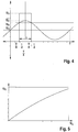
- the result is a profile of the reference voltage U R as a sensor signal or sensor variable A over the amplitude U a of the oscillation signal S or up (t), as shown in FIG Figure 5 is shown.
- the sensor variable A ie the reference voltage U R
- the evaluation circuit 20 is therefore suitable for using the reference voltage U R as a representative sensor variable A for the amplitude U a of the oscillation signal S or for the physical measured variable reflected in the amplitude U a of the oscillation signal S.
- the reference voltage U R is provided as a direct voltage, and therefore no further rectification is necessary.
- the comparator 25 as the only active electronic component of the evaluation circuit 20 can preferably be designed as a rail-to-rail comparator, a temperature dependency of the evaluation circuit 20 is measured on the output variable low and is limited in particular to only one switching threshold of the comparator 25.
- the feedback of the comparator output to the inverting input of the comparator 25 is provided to initiate an oscillation of the oscillating circuit 22 so that the oscillation can be maintained by the feedback of the comparator output to the oscillating circuit 22.
- the feedback to the inverting input of the comparator 25 takes place with the aid of a low-pass filter 26, this can also be used to provide the sensor variable A at the same time.
- the reference voltage U R corresponds to the sensor variable A, the potential of which depends on the amplitude U a of the oscillation signal S.
- this makes it possible to dispense with a device connected downstream of the comparator 25, for example a further low-pass filter, a rectifier or the like, and to use the reference voltage U R as the sensor variable A instead.
- a device connected downstream of the comparator 25 for example a further low-pass filter, a rectifier or the like, and to use the reference voltage U R as the sensor variable A instead.
- this provides an evaluation circuit 20 which manages without passive or active rectification and thereby reduces the number of components used and the total power consumption.
- Figure 6 shows the circuit diagram of a further embodiment of an evaluation circuit 30 for an inductive sensor with a sensor element 31 with an inductance L2, which forms an oscillating circuit 32 with a first and a second oscillating circuit capacitance C4, C5.
- the resonant circuit 32 is formed by an interconnection in which a first connection 35 of the inductance L2 via the first resonant circuit capacitance C4 with a low supply potential V GND , in particular a ground potential, and a second connection 36 of the inductance L2 via the second resonant circuit capacitance C5 with the low Supply potential V GND is connected.
- the second connection 36 of the inductance L2 provides the oscillation signal S to an inverting input of the comparator 33.
- the resonant circuit 32 can be excited at least predominantly in phase opposition via a feedback resistor R V2 via the first connection 35 of the inductance L2.
- the predetermined offset voltage U o is applied as a comparator threshold value KS to the non-inverting input of the comparator 33.
- the feedback resistor R V2 serves, in conjunction with the first resonant circuit capacitance C4, to cause the resonant circuit 32 to oscillate.
- the feedback resistor R V2 and the resonant circuit capacitances C4, C5 take over the task of the low-pass filter 26 and the feedback resistor R V2 also the task of maintaining the oscillation of the resonant circuit 32 through the feedback resistor R V of one of the previously described embodiments.
- a low-pass filter 34 connected downstream of the comparator 33 is provided in the form of an RC element, at the intermediate node of which the sensor variable A can be picked up as a direct voltage.
Landscapes
- Chemical & Material Sciences (AREA)
- Chemical Kinetics & Catalysis (AREA)
- Electrochemistry (AREA)
- Physics & Mathematics (AREA)
- Health & Medical Sciences (AREA)
- Life Sciences & Earth Sciences (AREA)
- Analytical Chemistry (AREA)
- Biochemistry (AREA)
- General Health & Medical Sciences (AREA)
- General Physics & Mathematics (AREA)
- Immunology (AREA)
- Pathology (AREA)
- Transmission And Conversion Of Sensor Element Output (AREA)
- Measuring Fluid Pressure (AREA)
Description
- Die Erfindung betrifft allgemein Sensoren, insbesondere Sensoren, die in einem Oszillator eingesetzt werden, wobei ein von einer physikalischen Messgröße abhängiges Schwingungssignal bereitgestellt wird. Weiterhin betrifft die vorliegende Erfindung Möglichkeiten zur Auswertung eines von einem Sensorelement beeinflussten Schwingungssignals, um eine Sensorgröße zu erhalten.
- Induktive oder kapazitive Sensorelemente werden häufig in kontaktlos arbeitenden Sensoranwendungen verwendet. Elektrische Eigenschaften von induktiven oder kapazitiven Sensorelementen können sich abhängig von einer physikalischen Messgröße ändern und werden üblicherweise mithilfe von Oszillatoren ausgewertet, um ein von der Messgröße abhängiges Schwingungssignal als Sensorsignal zu generieren.
- Zum Beispiel weist ein induktives Sensorelement eine Induktivität zumeist in Form einer Spule auf, die als Teil eines Oszillators mit einem elektrischen Schwingungssignal beaufschlagt wird. Die elektrische Schwingung bewirkt um die Induktivität ein Wechselmagnetfeld. Gelangt ein elektrisch leitender Körper in die Nähe der Induktivität, so bewirkt das Wechselmagnetfeld eine Induktion einer Spannung. Daraus resultieren Wirbelströme in dem Körper, die ein das Wechselmagnetfeld überlagerndes Störmagnetfeld generieren. In dem Oszillator kann sich eine durch das Störmagnetfeld hervorgerufene Impedanzänderung bzw. Störung des Wechselmagnetfeldes in Form einer Erhöhung einer Dämpfung auswirken.
- Eine Änderung der Dämpfung in einem Oszillator wirkt sich im Allgemeinen als eine Änderung der Amplituden der elektrischen Schwingung aus, die detektierbar und auswertbar ist. Zur Auswertung wird in herkömmlicher Weise das von dem Oszillator bereitgestellte elektrische Schwingungssignal zunächst mithilfe z.B. einer Diode gleichgerichtet, um eine von der Höhe der Impedanzänderung abhängige Sensorgröße in Form einer elektrischen Gleichgröße bereitzustellen.
- Derartige induktive Sensoren werden beispielsweise als induktive Näherungssensoren eingesetzt, um den Abstand eines elektrisch leitfähigen Objekts zum Sensor zu erfassen. Zum Bereitstellen eines für industrielle Anwendungen häufig benötigten binären Schaltsignals kann aus der Sensorgröße mithilfe eines Schmitt-Triggers oder Komparators eine binäre Sensorgröße erzeugt werden.
- Aus der Druckschrift
DE 10 2004 034 190 A1 ist eine Oszillatorschaltung für einen induktiven oder kapazitiven Sensor bekannt. Die Oszillatorschaltung umfasst einen Schwingkreis und einen Operationsverstärker, wobei eine elektrische Schwingung des Schwingkreises über zwei Anschlüsse differenziell abgegriffen und durch den Operationsverstärker verstärkt wird. - Aus der Druckschrift
EP 1 183 779 B1 ist ein Oszillator für einen induktiven Näherungssensor bekannt, der einen Schwingkreis und einen Komparator aufweist. Mithilfe eines Netzwerks mit positiver Rückkopplung wird der Ausgang des Komparators mit dem nicht invertierenden Eingang des Komparators verbunden. Weiterhin wird der Ausgang des Komparators mithilfe eines Netzwerks mit negativer Rückkopplung mit dem invertierenden Eingang des Komparators und dem Ausgang des Komparators verbunden, so dass Oszillationssignale unabhängig davon erzeugt werden, ob ein allmähliches oder schnelles Anlegen von Leistung an den Schwingkreis erfolgt. - Die Druckschrift
EP 0 537 747 A2 betrifft ein einen Näherungssensor mit einem Oszillator, dessen Schwingfrequenz sich abhängig von dem Abstand eines leitfähigen Objekts von dem Oszillator einstellt. Mithilfe eines Frequenz-Spannungswandlers wird die Schwingfrequenz des Oszillators in eine repräsentierende Spannung als Sensorgröße umgewandelt. - Die Druckschrift
EP 2 146 431 A2 beschreibt einen Näherungssensor mit einer Auswerteeinheit, die einen Oszillator, einen Gleichrichter und eine Signalwandlereinheit aufweist. Die Schwingfrequenz des Oszillators hängt in bekannter Weise von einem Abstand eines zu detektierenden Objekts ab. Die resultierende Schwingfrequenz wird in der Signalwandlereinheit ausgewertet. - Die obigen Druckschriften sehen zur Auswertung des von dem Oszillator erhaltenen Schwingungssignals vor, eine elektrische Wechselgröße bereitzustellen. Diese wird üblicherweise anschließend mithilfe eines oder mehrerer Halbleiterbauelemente, wie beispielsweise in einem Diodengleichrichter oder in einem aktiven Gleichrichter, gleichgerichtet, um eine verwertbare, die zu messende physikalische Messgröße repräsentierende Sensorgröße in Form einer elektrischen Gleichgröße bereitzustellen. Die Verwendung von Diodenschaltungen oder aktiven Gleichrichtern zum Zwecke der Gleichrichtung des Sensorsignals führt jedoch zu einer Temperaturabhängigkeit des Auswertungssignals, die insbesondere in Anwendungsbereichen mit hohen Temperaturschwankungen nachteilig ist.
- Auch sind Auswerteschaltungen, die auf einer dioden- oder gleichrichterbasierten Gleichrichtung des Schwingungssignals basieren, in der Regel aufwändig und weisen eine nennenswerte Leistungsaufnahme auf.
- Es ist daher Aufgabe der vorliegenden Erfindung, ein Verfahren und eine Schaltung zum Auswerten einer von einem Sensorelement erfassten physikalischen Messgröße bereitzustellen, die dazu in der Lage sind, basierend auf einem von der Messgröße abhängigen elektrischen Schwingungssignal eine Sensorgröße als elektrische Gleichgröße bereitzustellen, die eine nur geringe bzw. keine Temperaturabhängigkeit aufweist. Weiterhin soll die Auswerteschaltung eine geringere Anzahl von Bauelementen benötigen und eine geringe Leistungsaufnahme aufweisen.
- Diese Aufgabe wird durch das Verfahren zum Messen einer von einer physikalischen Messgröße abhängigen elektrischen Schwingungsgröße mit einem Sensorelement und zum Bereitstellen einer von der Messgröße abhängigen Sensorgröße gemäß Anspruch 1 sowie durch die Auswerteschaltung gemäß dem nebengeordneten Anspruch gelöst.
- Weitere Ausgestaltungen sind in den abhängigen Ansprüchen angegeben.
- Gemäß einem ersten Aspekt ist ein Verfahren zum Messen einer physikalischen Messgröße mit einem, insbesondere induktiven, Sensorelement und zum Bereitstellen einer von der Messgröße abhängigen Sensorgröße vorgesehen. Das Sensorelement ist Teil eines Schwingkreises, der eine von der physikalischen Messgröße abhängige Dämpfung aufweist. Der Schwingkreis wird angeregt, um ein periodisches Schwingungssignal zu generieren, dessen Amplitude von der Dämpfung abhängt. Weiterhin wird das Schwingungssignal mithilfe eines Komparators mit einem Komparatorschwellenwert verglichen, um ein periodisches Komparatorsignal mit einem von dem Komparatorschwellenwert abhängigen Tastverhältnis zu erhalten. Dabei wird der Komparatorschwellenwert gegenüber einem Mittelwert des Schwingungssignals so verstellt, dass sich ein von 50% verschiedenes Tastverhältnis einstellt. Die Sensorgröße kann dann als eine von dem Tastverhältnis des Komparatorsignals abhängige Größe bereitgestellt werden.
- Eine Idee des obigen Verfahrens besteht grundsätzlich darin, ein von einem elektrischen Schwingkreis mit einem Sensorelement bereitgestelltes Schwingungssignal, dessen Amplitude von der zu messenden physikalischen Messgröße abhängt, so auszuwerten, dass eine von der Amplitude des Schwingungssignals abhängige Sensorgröße als elektrische Gleichspannung bzw. Gleichstrom bereitgestellt wird.
- Bei herkömmlichen Ansätzen wird dazu das Schwingungssignal des Schwingkreises verstärkt und anschließend gleichgerichtet, zum Beispiel mithilfe einer Diode oder eines aktiven Gleichrichters, um das Sensorsignal zu erhalten. Da Halbleiterbauelemente in der Regel eine Temperaturabhängigkeit aufweisen, führt eine derartige Auswerteschaltung zu einer Sensorgröße, die von der Amplitude des Schwingungssignals, aber auch von der Temperatur der Auswerteschaltung abhängt. Dies kann insbesondere in einigen Einsatzgebieten nachteilig sein, in denen hohe Temperaturschwankungen auftreten können.
- Das obige Verfahren ermöglicht es auf einfache Weise, eine Auswerteschaltung mit einer reduzierten Anzahl von Bauelementen und insbesondere ohne die Verwendung eines Gleichrichters zum Bereitstellen der temperaturunabhängigen Sensorgröße als Gleichspannung bzw. Gleichstrom bereitzustellen. Die Temperaturunabhängigkeit wird im Wesentlichen dadurch erreicht, dass der Komparatorschwellenwert, bezüglich dessen das Schwingungssignal ausgewertet wird, abweichend von einem Mittelwert des Schwingungssignals eingestellt wird. Dadurch gibt der Komparatorschwellenwert eine Schaltschwelle vor, die vom Mittelwert des Schwingungssignals verschieden bzw. dazu verschoben ist. Dadurch erhält man am Ausgang des Komparators ein periodisches Komparatorsignal mit einem von 50% abweichenden Tastverhältnis.
- Das Einstellen des Komparatorsignals mit einem von 50% abweichenden Tastverhältnis basiert auf der durch den Komparatorschwellenwert eingestellten Schaltschwelle, die das periodische Schwingungssignal zu bestimmten Zeitpunkten über- bzw. unterschreitet. Diese Zeitpunkte hängen jedoch bei einer von dem Mittelwert des Schwingungssignals verschiedenen Schaltschwelle von der Steilheit des Schwingungssignals ab. Da die Steilheit des Schwingungssignals wiederum von der Amplitude des Schwingungssignals abhängt, ist das Tastverhältnis bei einer von dem Mittelwert des Schwingungssignals verschiedenen Schaltschwelle von der Amplitude des Schwingungssignals abhängig. Mit anderen Worten wird die Komparatorschwelle so eingestellt, dass das Schwingungssignal an einer zeitlichen Position abgetastet wird, die von der Amplitude des Schwingungssignals abhängig ist.
- Der Sensorgröße kann dann durch Bilden des Durchschnittswerts des Komparatorsignals, z. B. durch Glätten, erhalten werden. Dadurch wird ermöglicht, Dioden oder sonstige aktive Halbleiterbauelemente mit einer signifikanten Temperaturabhängigkeit für eine Gleichrichtung des Schwingungssignals zu vermeiden.
- Weiterhin kann der Mittelwert des Schwingungssignals gegenüber dem Komparatorschwellenwert mithilfe eines vorgegebenen Offsetwerts, insbesondere einer vorgegebenen Offsetspannung, verstellt werden, wobei das Schwingungssignal mit dem Offsetwert beaufschlagt wird oder der Komparatorschwellenwert dem Offsetwert entspricht oder abhängig von dem Offsetwert eingestellt wird.
- Es kann vorgesehen sein, dass der Komparatorschwellenwert abhängig von dem Tastverhältnis des periodischen Komparatorsignals eingestellt wird.
- Insbesondere kann der Komparatorschwellenwert als der, insbesondere durch Glätten, erhaltene Durchschnittswert des periodischen Komparatorsignals eingestellt werden, wobei die Sensorgröße dem Durchschnittswert entspricht.
- Gemäß einer Ausführungsform kann eine Oszillation des Schwingkreises durch gleichphasige Rückkopplung des periodischen Komparatorsignals aufrechterhalten werden.
- Das Komparatorsignal kann tiefpassgefiltert werden, wobei ein Anschwingen des Schwingkreises durch Rückkopplung des tiefpassgefilterten Komparatorsignals auf den Komparatorschwellenwert bewirkt wird.
- Gemäß einer Ausführungsform kann der Komparatorschwellenwert abhängig von dem Tastverhältnis des periodischen Komparatorsignals und abhängig von einem vorgegebenen Offsetwert gegenüber einem Mittelwert des Schwingungssignals verstellt werden, so dass sich ein Gleichgewichtszustand zwischen einem sich aufgrund des vorgegebenen Offsetwerts einstellenden Tastverhältnis und einem sich abhängig von dem Komparatorschwellenwert einstellenden Tastverhältnis ergibt.
- Dadurch wird eine Rückkopplung von dem Ausgang des Komparators vorgesehen, wodurch der Komparatorschwellenwert abhängig von dem Tastverhältnis des Komparatorsignals am Ausgang des Komparators eingestellt wird. Die Abhängigkeit kann so gewählt sein, dass mit einer ansteigenden Abweichung des Tastverhältnisses von 50 % der Komparatorschwellenwert zunehmend in Richtung des Mittelwerts des Schwingungssignals verschoben wird. Auf diese Weise stellt sich am Ausgang des Komparators ein Tastverhältnis des Komparatorsignals ein, das von der Verstimmung des Komparatorschwellenwerts gegenüber dem Mittelwert des Schwingungssignals und der Amplitude des Schwingungssignals abhängt. Somit kann als Sensorgröße der Komparatorschwellenwert als Gleichspannung herangezogen werden.
- Insbesondere die Abweichung zwischen dem vorgegebenen Offsetwert und dem sich aus dem Tastverhältnis des Komparatorsignals ergebenden Komparatorschwellenwert führt dazu, dass sich ein Gleichgewichtszustand einstellt. Dadurch entsteht eine Abhängigkeit zwischen dem Komparatorschwellenwert und der Amplitude des periodischen Schwingungssignals. Die Bereitstellung des Komparatorschwellenwerts als von der Amplitude des Schwingungssignals abhängige Gleichspannung ermöglicht es, auf eine Gleichrichtung des Komparatorausgangssignals zu verzichten und den Komparatorschwellenwert als bereitgestellte Sensorgröße zu verwenden.
- Weiterhin kann die Messgröße einer Spannung des Komparatorschwellenwerts oder einer effektiven, durch Glättung des periodischen Komparatorsignals erhaltenen Spannung entsprechen.
- Gemäß einer weiteren Ausführungsform kann der Schwingkreis gegenphasig durch das periodische Komparatorsignal angeregt werden.
- Gemäß einem weiteren Aspekt kann eine Auswerteschaltung zum Messen einer physikalischen Messgröße mit einem, insbesondere induktiven, Sensorelement und zum Bereitstellen einer von der Messgröße abhängigen Sensorgröße vorgesehen sein, wobei die Auswerteschaltung umfasst:
- einen das Sensorelement umfassenden Schwingkreis, der eine von der physikalischen Messgröße abhängige Dämpfung aufweist;
- eine Einrichtung zum Bereitstellen eines Anregungssignals zum Anregen des Schwingkreises, um ein periodisches Schwingungssignal zu generieren, dessen Amplitude von der Dämpfung des Schwingkreises abhängt;
- einen Komparator, um das Schwingungssignal mit einem Komparatorschwellenwert zu vergleichen, so dass ein resultierendes periodisches Komparatorsignal mit einem von dem Komparatorschwellenwert abhängigen Tastverhältnis bereitgestellt wird, wobei die Sensorgröße als eine von dem Tastverhältnis des Komparatorsignals abhängige Größe bereitgestellt wird; und
- eine Einrichtung zum Verstellen des Komparatorschwellenwerts gegenüber einem Mittelwert des Schwingungssignals, so dass sich ein von 50% verschiedenes Tastverhältnisses einstellt.
- Weiterhin kann eine Offsetspannungsquelle vorgesehen sein, um den Mittelwert des Schwingungssignals gegenüber dem Komparatorschwellenwert mithilfe eines vorgegebenen Offsetwerts, insbesondere einer vorgegebenen Offsetspannung, zu verstellen, wobei die Offsetspannungsquelle so geschaltet ist, dass das Schwingungssignal mit dem Offsetwert beaufschlagt wird oder der Komparatorschwellenwert dem Offsetwert entspricht oder abhängig von dem Offsetwert eingestellt wird.
- Die Einrichtung zum Bereitstellen des Anregungssignals kann durch eine Rückkopplung des Komparatorsignals, insbesondere mithilfe eines Rückkopplungswiderstands, auf den Schwingkreis vorgesehen sein, um den Schwingkreis durch das periodische Komparatorsignal anzuregen, so dass dieser insbesondere bei seiner Resonanzfrequenz kontinuierlich schwingt.
- Insbesondere kann eine Anschwingeinrichtung vorgesehen sein, um das periodische Komparatorsignal tiefpasszufiltern und um den Komparatorschwellenwert als das tiefpassgefilterte Komparatorsignal oder als ein von dem tiefpassgefilterten Komparatorsignal abhängiges Signal bereitzustellen, um ein Anschwingen des Schwingkreises zu ermöglichen, wobei das tiefpassgefilterte Komparatorsignal als die Sensorgröße bereitgestellt wird.
- Das Sensorelement kann eine Induktivität aufweisen, wobei der Schwingkreis die Induktivität aufweist, deren Anschlüsse jeweils über Schwingkreiskapazitäten mit einem festgelegten Potenzial gekoppelt sind, wobei die Rückkopplung des Komparatorsignals auf den Schwingkreis gegenphasig erfolgt.
- Ausführungsformen werden nachfolgend anhand der beigefügten Zeichnungen näher erläutert. Es zeigen:
- Fig. 1
- eine schematische Darstellung einer Auswerteschaltung für einen Sensor;
- Fig. 2
- eine Darstellung eines Verlaufs zweier beispielhafter Schwingungssignale verschiedener Amplitude sowie der daraus resultierenden Komparatorsignale;
- Fig. 3
- eine Darstellung einer Ausführungsform einer Auswerteschaltung für einen induktiven Sensor;
- Fig. 4
- eine schematische Darstellung des zeitlichen Verlaufs des Schwingungssignals als ein idealisiert sinusförmiges Signal;
- Fig. 5
- eine schematische Darstellung der nahezu linearen Abhängigkeit zwischen der Amplitude des Schwingungssignals und der Ausgangsgröße; und
- Fig. 6
- eine Darstellung eines Schaltplans für eine Auswerteschaltung für einen induktiven Sensor gemäß einer weiteren Ausführungsform.
-
Figur 1 zeigt eine schematische Darstellung einer Auswerteschaltung 1 für ein Sensorelement 2, das Teil eines Schwingkreises 3 bzw. Oszillators ist. Das Sensorelement 2 dient zum Erfassen einer physikalischen Messgröße und zum Beeinflussen des Schwingkreises 3 derart, dass ein periodisches Schwingungssignal mit einer von der physikalischen Messgröße abhängigen Amplitude generiert wird. Beispielsweise kann das Sensorelement 2 so gewählt sein, dass eine Änderung der zu erfassenden physikalischen Messgröße zu einer Impedanzänderung des Sensorelements 2 führt. Die Impedanzänderung resultiert in dem Schwingkreis 3 in einer veränderten Dämpfung des periodischen Schwingungssignals, die ausgewertet werden kann. - Der Schwingkreis 3 wird mithilfe einer Anregungseinrichtung 4 kontinuierlich zum Bereitstellen des periodischen Schwingungssignals S angeregt. Die Anregungseinrichtung 4 dient einerseits dazu, beim Starten der Auswerteschaltung 1 ein Anschwingen des Schwingkreises 3 zu bewirken, und andererseits dazu, ein kontinuierliches Schwingen des Schwingkreises 3 durch Einbringen gleichbleibender Anregungsenergie aufrecht zu erhalten. Insbesondere erfolgt die Anregung durch Beaufschlagen mit einem Anregungssignal, das einen Frequenzanteil mit einer Resonanzfrequenz des Schwingkreises 3 aufweist.
- Das periodische Schwingungssignal S wird einem ersten Eingang E1 eines Komparators 5 zugeführt und dort mit einem an einem zweiten Eingang E2 bereitgestellten vorgegebenen Komparatorschwellenwert KS, insbesondere in Form einer Spannung, verglichen. Ein am Ausgang des Komparators 5 resultierendes Komparatorsignal K entspricht einem Rechteckspannungssignal mit der Periodizität des periodischen Schwingungssignals S.
- Der Komparatorschwellenwert KS kann von einer Offset-Einheit 7 vorgegeben werden, die beispielsweise als eine mit dem zweiten Eingang E2 des Komparators 5 verbundene Offsetspannungsquelle 7 ausgebildet sein kann.
- Die Offset-Einheit 7 dient dazu, mithilfe eines Offsetwerts O, der als eine Offsetspannung Uo angegeben werden kann, den Komparatorschwellenwert KS so vorzugeben, dass dieser gegenüber einem Mittelwert des Schwingungssignals S verschoben bzw. von dem Mittelwert des Schwingungssignals S verschieden ist.
- Als Mittelwert kann ein mittlerer Wert aus einem Maximum und einem Minimum des Schwingungssignals verwendet werden. Als Mittelwert kann auch das durch die Periodendauer der Schwingung dividierte Integral des Verlaufs des Schwingungssignals über eine Periodendauer verwendet werden.
- Das Schwingungssignal S kann im Wesentlichen einem elektrischen Signal mit nahezu sinusförmigem Verlauf entsprechen, wobei ein Mittelwert aus dem maximalen und dem minimalen Signalwert bestimmt sein kann. Die durch den Komparatorschwellenwert KS definierte Komparatorschwelle bezüglich des Schwingungssignals S wird dann als ein Wert zwischen dem Mittelwert und dem maximalen Wert oder zwischen dem Mittelwert und dem minimalen Wert des Schwingungssignals S vorgegeben. Auf diese Weise kann der Komparatorschwellenwert KS gegenüber dem Mittelwert des Schwingungssignals S verstimmt werden.
- Das Komparatorsignal K am Ausgang des Komparators 5 wird einem Tiefpassfilter 6 zugeführt, der z. B. als RC-Glied ausgebildet ist. Der Tiefpassfilter 6 dient dazu, das Komparatorsignal K zu glätten und eine zu dem Tastverhältnis des Komparatorsignals K proportionale Sensorgröße A als elektrische Gleichgröße, insbesondere als Sensorspannung, bereitzustellen.
- Würde der Komparatorschwellenwert KS auf den Mittelwert des Schwingungssignals S eingestellt, so stellte sich am Ausgang des Komparators 5 ein Komparatorsignal K mit einem Tastverhältnis von 50% ein. Beim Verstellen des Komparatorschwellenwerts KS bezüglich des Mittelwerts des Schwingungssignals S ergibt sich ein Tastverhältnis des Komparatorsignals K, das von 50% abweicht, da die Schaltschwelle des Komparators 5 die sinusförmige Verlaufskurve des Schwingungssignals S zu von dem Nulldurchgang verschiedenen Zeitpunkten schneidet.
- Das Tastverhältnis, das sich aufgrund des bezüglich des Mittelwerts des Schwingungssignals S verstimmten Komparatorschwellenwerts KS ergibt, hängt zum einen von dem Betrag des Komparatorschwellenwerts KS bzw. von dessen Abstand zum Mittelwert des Schwingungssignals S ab und zum anderen von der Amplitude des Schwingungssignals S. Wie aus dem in
Fig. 2 dargestellten Verlauf zweier beispielhafter sinusförmiger Schwingungssignale S1, S2 verschiedener Amplitude ersichtlich ist, ergibt sich das sich einstellende Tastverhältnis des Komparatorsignals K aus den unterschiedlichen Steilheiten des Schwingungssignals S zum Zeitpunkt der durch den Komparatorschwellenwert KS bestimmten Schaltschwellen. So ist bei einer Periodendauer T und bei einem ersten Schwingungssignal S1 mit geringerer Amplitude das Tastverhältnis ts1/T des resultierenden ersten Komparatorsignals K1 geringer als das Tastverhältnis ts2/T des resultierenden zweiten Komparatorsignals K2 bei dem zweiten Schwingungssignal S2 mit höherer Amplitude, wobei ts1 und ts2 die Zeitdauern angeben, zu denen das jeweilige Schwingungssignal S, S1, S2 einen größeren Signalwert aufweist als der Komparatorschwellenwert KS vorgibt. - In alternativen Ausführungsformen kann auch das Schwingungssignal S mit dem Offsetwert O beaufschlagt werden, indem die Offset-Einheit 7 im Signalpfad des Schwingkreises 3 angeordnet wird. Dadurch addieren sich der Offsetwert O und das Schwingungssignal S. An den zweiten Eingang E2 des Komparators 5 wird dann lediglich ein vorgegebener Vergleichswert, z. B. in Form eines vorgegeben Spannungspotenzials, angelegt. Selbstverständlich muss für die Dimensionierung des Offsetwerts O, des Vergleichswerts und des Schwingkreises 3 der Arbeitsbereich des Komparators 5 berücksichtigt werden.
- In
Fig. 3 ist als Beispiel für die Auswerteschaltung 1 ein konkreteres Schaltbild für eine Auswerteschaltung 20 für einen induktiven Sensor dargestellt. Der induktive Sensor umfasst ein Sensorelement 21, das im dargestellten Schaltbild als eine Induktivität L1 dargestellt ist. Die Induktivität L1 ist parallel zu zwei in Serie geschalteten Schwingkreiskapazitäten C2 und C3 geschaltet, um einen Schwingkreis 22 auszubilden. Eine Oszillation des Schwingkreises 22 führt zu einem Wechselstrom durch die als Spule ausgeführte Induktivität L1, wodurch ein Wechselmagnetfeld ausgebildet wird. - Bei Verwendung des induktiven Sensors als induktiver Näherungssensor kann erfasst werden, ob ein Gegenstand mit einem elektrisch leitenden Element seine Position in dem Wechselmagnetfeld ändert bzw. durch Annäherung an den induktiven Sensor in das Wechselmagnetfeld gelangt. Dies bewirkt in elektrisch leitenden Elementen die Entstehung von Wirbelströmen, die mit dem Wechselmagnetfeld wechselwirken und zu einer Störung des erzeugten Wechselmagnetfeldes führen. Diese Störung des Wechselmagnetfeldes wirkt sich als veränderte Impedanz des Sensorelements 21 bzw. als veränderte Dämpfung der Schwingung im Schwingkreis 22 aus. Diese Dämpfung wird daher durch den parallel zu der Induktivität L1 geschalteten Widerstand Rp im Schwingkreis 22 elektrisch abgebildet.
- Der Schwingkreis 22 ist als Parallelschwingkreis ausgebildet und weist einen ersten Anschluss 23 auf, der mit einer vorgegebenen Offsetspannung Uo aus einer entsprechenden Offsetspannungsquelle 27 beaufschlagt ist, und einen zweiten Anschluss 24, der an einem nicht invertierenden Eingang eines Komparators 25 angelegt ist. Der Komparator 25 kann beispielsweise als Differenzverstärker oder Operationsverstärker ausgebildet sein. Somit liegt an dem nicht invertierenden Eingang des Komparators 25 eine Spannung an, die einer Summe aus der Offsetspannung Uo und einer Schwingkreisspannung, die dem Schwingungssignal S entspricht, an.
- Der Komparator 25 wird mit einer Versorgungsspannung Uv, d. h. einer Spannung zwischen einem hohen Versorgungspotenzial Vv und einem niedrigen Versorgungspotenzial VGND, insbesondere einem Massepotenzial, mit elektrischer Energie versorgt. Der Komparator 25 ist vorzugsweise als Rail-to-Rail-Komparator ausgebildet, d. h. es wird bei positivem Bewertungsergebnis im Wesentlichen das hohe Versorgungspotenzial Vv und bei einem negativen Bewertungsergebnis das niedrige Versorgungspotenzial VGND am Komparatorausgang als Komparatorsignal K, das vorzugsweise einem Spannungssignal entspricht, ausgegeben.
- Das Komparatorsignal K ist über einen Rückkopplungswiderstand Rv in einen Knoten zwischen die beiden Schwingkreiskapazitäten C2 und C3 eingekoppelt, um eine permanente Anregung für den Schwingkreis 22 bereitzustellen, so dass sich in dem Schwingkreis 22 ein konstantes Oszillationsverhalten bei dessen Resonanzfrequenz ergibt. Dies ist möglich, da das Komparatorsignal K als Rechtecksignal eine Periode aufweist, die der Periode des Schwingungssignals S entspricht. Dadurch weist das Komparatorsignal K selbst bei einem Tastverhältnis von ungleich 50% einen Frequenzanteil auf, der zur vorwiegend gleichphasigen Anregung des Schwingkreises 22 über die Rückkopplung des Rückkopplungswiderstands Rv genügt. Es ist selbstverständlich ebenfalls möglich, die Anregung des Schwingkreises 22 und das Aufrechterhalten der Oszillation durch eine separate Anregungseinrichtung 4, die von dem Komparatorsignal K unabhängig ist, zu bewirken.
- Das Komparatorsignal K, das im Wesentlichen ein Rechtecksignal mit einem Tastverhältnis und mit Signalpegeln ist, die dem hohen Versorgungspotenzial Vv und dem niedrigen Versorgungspotenzial VGND entsprechen, wird über einen Tiefpassfilter 26 auf einen invertierenden Eingang des Komparators 25 rückgekoppelt. Der Tiefpassfilter 26 umfasst einen Filterwiderstand R1 und eine Filterkapazität C1, die in Reihe geschaltet sind, so dass sich an einem Knoten zwischen dem Filterwiderstand R1 und der Filterkapazität C1 eine Referenzspannung UR ergibt, die als Komparatorschwellenwert KS bzw. als Komparatorschwellenspannung an den invertierenden Eingang des Komparators 25 angelegt ist.
- Der so gebildete Tiefpassfilter 26 ist so ausgebildet, dass beim Einschalten der Auswerteschaltung 20 an dem invertierenden Eingang des Komparators 25 die Referenzspannung UR mit zu Beginn starkem und anschließend abnehmendem Schwingen anliegt. Die zu Beginn starke Welligkeit der Referenzspannung UR führt zu einem wechselnden Signalpegel des Komparatorsignals K, das durch den Rückkopplungswiderstand Rv in den Knoten zwischen die beiden Schwingkreiskapazitäten C2 und C3 eingekoppelt wird. Dadurch unterstützt die Rückkopplung auf den invertierenden Eingang des Komparators 25 das Anschwingen durch anfängliches Erzeugen eines Komparatorsignals K mit periodisch wechselnden Signalpegeln bis der Schwingkreis 22 basierend auf der Rückkopplung durch den Rückkopplungswiderstand Rv die Oszillation aufgenommen hat.
- Im eingeschwungenen Zustand bewirkt der Tiefpassfilter 26 weiterhin die Bereitstellung der Referenzspannung UR an dem invertierenden Eingang des Komparators 25, die durch Glättung des Komparatorsignals K im Wesentlichen als Gleichspannung bereitgestellt wird.
- Im Wesentlichen stellt sich dadurch als Referenzspannung UR eine Spannung ein, die durch das sich im eingeschwungenen Zustand des Schwingkreises 22 einstellende Tastverhältnis des Komparatorsignals K sowie durch das hohe Versorgungspotenzial Vv und das niedrige Versorgungspotenzial VGND gebildet wird. Durch den Komparator 25 bzw. die Potenziale des hohen und niedrigen Pegels sowie durch den Tiefpassfilter 26 wird die Referenzspannung UR so gebildet, dass eine von dem Tastverhältnis des Komparatorsignals K abhängige Spannung an dem invertierenden Eingang des Komparators 25 anliegt. Im vorliegenden Ausführungsbeispiel entspricht die Referenzspannung UR bei einem Tastverhältnis von 50% der halben Versorgungsspannung Uv/2.
- Im wesentlichen weist das in dem Schwingkreis 22 generierte Schwingungssignal einen sinusförmigen Verlauf auf, dessen Mittelwert durch die Offsetspannung Uo bestimmt ist. Ist die Auswerteschaltung 20 abgestimmt, d. h. die Offsetspannung Uo entspricht der Referenzspannung UR, so stellt sich als Komparatorsignal K am Ausgang des Komparators 25 ein Signal mit einem Tastverhältnis von 50% ein. Die Auswerteschaltung 20 ist dagegen verstimmt, wenn die sich aus dem Tastverhältnis des Komparatorsignals K ergebende Referenzspannung UR einem anderen Spannungsniveau als der Offsetspannung Uo entspricht. Die Verstimmung bewirkt, dass das mit der Offsetspannung Uo beaufschlagte Schwingungssignal up(t) nicht mit einem Komparatorschwellenwert KS abgetastet wird, der dem Mittelwert des Schwingungssignals up(t) entspricht, und am Ausgang des Komparators 25 ein Komparatorsignal K generiert wird, dessen Tastverhältnis von einem Tastverhältnis von 50% abweicht. Dadurch ändert sich die Referenzspannung UR und es stellt sich ein Gleichgewichtszustand ein, in dem das sich einstellende Tastverhältnis des Komparatorsignals K eine Referenzspannung UR bewirkt, die von dem Mittelwert der Schwingung so abweicht, das sich als Komparatorsignal K ein Signal mit dem entsprechenden Tastverhältnis einstellt.
- In
Figur 4 ist für die Auswerteschaltung 20 derFigur 3 schematisch der zeitliche Verlauf des Schwingungssignals S als ein idealisiert sinusförmiges Signal dargestellt. Es gilt:
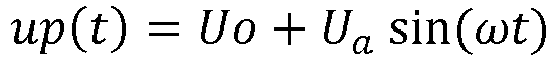


- Daraus folgt:


- Es ergibt sich ein Verlauf der Referenzspannung UR als Sensorsignal bzw. Sensorgröße A über der Amplitude Ua des Schwingungssignals S bzw. up(t), wie es in
Figur 5 dargestellt ist. Man erkennt, dass die Sensorgröße A, d.h. die Referenzspannung UR, im Wesentlichen einer Gleichspannung entspricht, die etwa linear zur Amplitude Ua des Schwingungssignals up(t) verläuft. Somit ist die Auswerteschaltung 20 geeignet, die Referenzspannung UR als repräsentative Sensorgröße A für die Amplitude Ua des Schwingungssignals S bzw. für die sich in der Amplitude Ua des Schwingungssignals S widerspiegelnde physikalische Messgröße heranzuziehen. Das Bereitstellen der Referenzspannung UR erfolgt als Gleichspannung, und somit ist keine weitere Gleichrichtung notwendig. - Da der Komparator 25 als einziges aktives elektronisches Bauelement der Auswerteschaltung 20 vorzugsweise als Rail-to-Rail-Komparator ausgebildet werden kann, ist eine Temperaturabhängigkeit der Auswerteschaltung 20 gemessen an der Ausgangsgröße gering und beschränkt sich insbesondere nur auf eine Schaltschwelle des Komparators 25.
- Im Wesentlichen ist die Rückkopplung des Komparatorausgangs auf den invertierenden Eingang des Komparators 25 dazu vorgesehen, ein Anschwingen des Schwingkreises 22 zu initiieren, so dass durch die Rückkopplung des Komparatorausgangs auf den Schwingkreis 22 die Schwingung aufrechterhalten werden kann. Da jedoch die Rückkopplung auf den invertierenden Eingang des Komparators 25 mithilfe eines Tiefpassfilters 26 erfolgt, kann dieser auch gleichzeitig zur Bereitstellung der Sensorgröße A genutzt werden. Mit anderen Worten entspricht die Referenzspannung UR der Sensorgröße A, deren Potenzial von der Amplitude Ua des Schwingungssignals S abhängt. Dadurch ist es möglich auf eine dem Komparator 25 nachgeschaltete Einrichtung, wie beispielsweise einen weiteren Tiefpassfilter, einen Gleichrichter oder dergleichen, zu verzichten und stattdessen die Referenzspannung UR als Sensorgröße A zu verwenden. Insgesamt wird dadurch eine Auswertungsschaltung 20 zur Verfügung gestellt, die ohne passive oder aktive Gleichrichtung auskommt und dadurch die Anzahl der verwendeten Bauelemente und die gesamte Stromaufnahme reduziert.
-
Figur 6 zeigt das Schaltbild einer weiteren, gegenüber der Auswerteschaltung 1 konkretisierten Ausführungsform einer Auswerteschaltung 30 für einen induktiven Sensor mit einem Sensorelement 31 mit einer Induktivität L2, die mit einer ersten und einer zweiten Schwingkreiskapazität C4, C5 einen Schwingkreis 32 bildet. Der Schwingkreis 32 wird gebildet durch eine Verschaltung, bei der ein erster Anschluss 35 der Induktivität L2 über die erste Schwingkreiskapazität C4 mit einem niedrigen Versorgungspotenzial VGND, insbesondere einem Massepotenzial, und ein zweiter Anschluss 36 der Induktivität L2 über die zweite Schwingkreiskapazität C5 mit dem niedrigen Versorgungspotenzial VGND verbunden ist. Störungen im Wechselmagnetfeld der als Spule ausgebildeten Induktivität L2 führen zu einer Impedanzänderung bzw. einer Dämpfung einer Schwingung des Schwingkreises 32, die im Schaltbild durch den parallel zur Induktivität L2 geschalteten Widerstand RP2 abgebildet wird. - Der zweite Anschluss 36 der Induktivität L2 stellt das Schwingungssignal S an einen invertierenden Eingang des Komparators 33 bereit. Dadurch kann der Schwingkreis 32 über einen Rückkopplungswiderstand RV2 über den ersten Anschluss 35 der Induktivität L2 zumindest vorwiegend gegenphasig angeregt werden. An dem nicht invertierenden Eingang des Komparators 33 ist die vorgegebene Offsetspannung Uo als Komparatorschwellenwert KS angelegt.
- Der Rückkopplungswiderstand RV2 dient dazu, in Verbindung mit der ersten Schwingkreiskapazität C4 ein Anschwingen des Schwingkreises 32 zu bewirken. Somit übernehmen der Rückkopplungswiderstand RV2 und die Schwingkreiskapazitäten C4, C5 die Aufgabe des Tiefpassfilters 26 und der Rückkopplungswiderstand RV2 ebenfalls die Aufgabe des Aufrechterhaltens der Schwingung des Schwingkreises 32 durch den Rückkopplungswiderstand RV einer der zuvor beschriebenen Ausführungsformen.
- Insbesondere sind in der Auswerteschaltung 30 der Ausführungsform der
Figur 6 durch die Verschaltung der Schwingkreiskapazitäten C4 und C5 alle signalführenden Knoten kapazitiv mit dem niedrigen Versorgungspotenzial VGND verbunden. Dadurch ermöglicht der Aufbau des Schwingkreises 32 und dessen gegenphasige Anregung einen Aufbau der Auswerteschaltung 30 , mit dem Störeinflüsse auf die Auswerteschaltung 30 deutlich reduziert werden können. - Das Funktionsprinzip der Ausführungsform der
Figur 6 entspricht dem der zuvor beschriebenen Ausführungsformen. Mithilfe der Offsetspannung UO wird ein Komparatorschwellenwert KS vorgegeben, durch den die Schaltung verstimmt werden kann. Auf diese Weise stellt sich ein von 50 % verschiedenes Tastverhältnis am Komparatorausgang ein, das sich aus der Offsetspannung UO und dem Spannungsniveau des Mittelwerts des Schwingungssignals S ergibt. - Zum Bereitstellen der Sensorgröße A ist ein dem Komparator 33 nachgeschalteter Tiefpassfilter 34 in Form eines RC-Gliedes vorgesehen, an dessen Zwischenknoten die Sensorgröße A als Gleichspannung abgenommen werden kann.
-
- 1
- Auswerteschaltung
- 2
- Sensorelement
- 20
- Auswerteschaltung
- 21
- Sensorelement
- 22
- Schwingkreis
- 23
- erster Anschluss
- 24
- zweiter Anschluss
- 25
- Komparator
- 26
- Tiefpassfilter
- 27
- Offsetspannungsquelle
- 3
- Schwingkreis
- 30
- Auswerteschaltung
- 31
- induktiver Sensor
- 32
- Schwingkreis
- 33
- Komparator
- 34
- Tiefpassfilter
- 35
- erster Anschluss der Induktivität L2
- 36
- zweiter Anschluss der Induktivität L2
- 37
- Phasenkorrektureinheit
- 4
- Anregungseinrichtung
- 5
- Komparator
- 6
- Tiefpassfilter
- 7
- Offset-Einheit
- A
- Sensorgröße (Sensorsignal)
- C1
- Filterkapazität
- C2, C3, C4, C5
- Schwingkreiskapazitäten
- E1
- erster Eingang
- E2
- zweiter Eingang
- K
- Komparatorsignal
- K1
- erstes resultierendes Komparatorsignal
- K2
- zweites resultierendes Komparatorsignal
- KS
- Komparatorschwellenwert
- L1, L2
- Induktivitäten
- O
- Offsetwert
- R1
- Filterwiderstand
- RP
- Widerstand
- RP2
- Widerstand
- RV
- Rückkopplungswiderstand
- S
- Schwingungssignal
- S1
- erstes sinusförmiges Schwingungssignal
- S2
- zweites sinusförmiges Schwingungssignal
- ts1, ts2
- Zeitdauer
- T
- Periodendauer
- UO
- Offsetspannung
- Ua
- Amplitude des Schwingungssignals
- UR
- Referenzspannung
- VGND
- niedriges Versorgungspotenzial
- VV
- hohes Versorgungspotenzial
Claims (14)
- Verfahren zum Messen einer physikalischen Messgröße mit einem, insbesondere induktiven, Sensorelement (2, 21, 31) und zum Bereitstellen einer von der Messgröße abhängigen Sensorgröße (A),
wobei das Sensorelement (2, 21, 31) Teil eines Schwingkreises (3, 22, 32) ist, der eine von der physikalischen Messgröße abhängige Dämpfung aufweist,
wobei der Schwingkreis (3, 22, 32) angeregt wird, um ein periodisches Schwingungssignal (S, S1, S2) zu generieren, dessen Amplitude (Ua) von der Dämpfung abhängt;
wobei das Schwingungssignal (S, S1, S2) mithilfe eines Komparators (5, 25, 33) mit einem Komparatorschwellenwert (KS) verglichen wird, um ein periodisches Komparatorsignal (K) mit einem von dem Komparatorschwellenwert (KS) abhängigen Tastverhältnis zu erhalten,
dadurch gekennzeichnet, dass der Komparatorschwellenwert (KS) gegenüber einem Mittelwert des Schwingungssignals (S, S1, S2) so verstellt wird, dass sich ein von 50% verschiedenes Tastverhältnis einstellt,
wobei die Sensorgröße (A) als eine von dem Tastverhältnis des Komparatorsignals (K) abhängige Größe bereitgestellt wird. - Verfahren nach Anspruch 1, wobei ein Mittelwert des Schwingungssignals (S, S1, S2) gegenüber dem Komparatorschwellenwert (KS) mithilfe eines vorgegebenen Offsetwerts (O), insbesondere einer vorgegebenen Offsetspannung (Uo), verstellt wird, wobei das Schwingungssignal (S, S1, S2) mit dem Offsetwert (O) beaufschlagt wird oder der Komparatorschwellenwert (KS) dem Offsetwert (O) entspricht oder abhängig von dem Offsetwert (O) eingestellt wird.
- Verfahren nach Anspruch 1 oder 2, wobei der Komparatorschwellenwert (KS) abhängig von dem Tastverhältnis des periodischen Komparatorsignals (K) eingestellt wird.
- Verfahren nach Anspruch 3, wobei der Komparatorschwellenwert (KS) als der, insbesondere durch Glätten erhaltene, Durchschnittswert des periodischen Komparatorsignals (K) eingestellt wird, wobei die Sensorgröße (A) dem Durchschnittswert entspricht.
- Verfahren nach einem der Ansprüche 1 bis 4, wobei eine Oszillation des Schwingkreises (3, 22) durch gleichphasige Rückkopplung des periodischen Komparatorsignals (K) aufrechterhalten wird.
- Verfahren nach einem der Ansprüche 1 bis 5, wobei das Komparatorsignal (K) tiefpassgefiltert wird, wobei ein Anschwingen des Schwingkreises (3, 22) durch Rückkopplung des tiefpassgefilterten Komparatorsignals (K) auf den Komparatorschwellenwert (KS) bewirkt wird.
- Verfahren nach einem der Ansprüche 1 bis 6, wobei der Komparatorschwellenwert (KS) abhängig von dem Tastverhältnis des periodischen Komparatorsignals (K) und abhängig von einem vorgegebenen Offsetwert (O) gegenüber einem Mittelwert des Schwingungssignals (S, S1, S2) verstellt wird, so dass sich ein Gleichgewichtszustand zwischen einem sich aufgrund des vorgegebenen Offsetwerts (O) einstellenden Tastverhältnis und einem sich abhängig von dem Komparatorschwellenwert (KS) einstellenden Tastverhältnis ergibt.
- Verfahren nach einem der Ansprüche 1 bis 7, wobei die Messgröße einer Spannung des Komparatorschwellenwerts (KS) oder einer effektiven, durch Glättung des periodischen Komparatorsignals (K) erhaltenen Spannung entspricht.
- Verfahren nach einem der Ansprüche 1 bis 4, wobei der Schwingkreis (32) gegenphasig durch das periodische Komparatorsignal (K) angeregt wird.
- Auswerteschaltung (1,20, 30) zum Messen einer physikalischen Messgröße mit einem, insbesondere induktiven, Sensorelement (2, 21, 31) und zum Bereitstellen einer von der Messgröße abhängigen Sensorgröße (A), wobei die Sensorgröße (A) als eine von dem Tastverhältnis des Komparatorsignals (K) abhängige Größe bereitgestellt wird; umfassend:- einen das Sensorelement (2, 21, 31) umfassenden Schwingkreis (3, 22, 32), der eine von der physikalischen Messgröße abhängige Dämpfung aufweist;- eine Einrichtung zum Bereitstellen eines Anregungssignals zum Anregen des Schwingkreises (3, 22, 32), um ein periodisches Schwingungssignal (S, S1, S2) zu generieren, dessen Amplitude (Ua) von der Dämpfung des Schwingkreises (3, 22, 32) abhängt;- einen Komparator (5, 25, 33), um das Schwingungssignal (S, S1, S2) mit einem Komparatorschwellenwert (KS) zu vergleichen, so dass ein resultierendes periodisches Komparatorsignal (K) mit einem von dem Komparatorschwellenwert (KS) abhängigen Tastverhältnis bereitgestellt wird;
gekennzeichnet durch:- eine Einrichtung zum Verstellen des Komparatorschwellenwerts (KS) gegenüber einem Mittelwert des Schwingungssignals (S, S1, S2), so dass sich ein von 50% verschiedenes Tastverhältnis einstellt. - Auswerteschaltung (1, 20, 30) nach Anspruch 10, wobei eine Offsetspannungsquelle (27) vorgesehen ist, um den Mittelwert des Schwingungssignals (S, S1, S2) gegenüber dem Komparatorschwellenwert (KS) mithilfe eines vorgegebenen Offsetwerts (O), insbesondere einer vorgegebenen Offsetspannung (Uo), zu verstellen, wobei die Offsetspannungsquelle (27) so geschaltet ist, dass das Schwingungssignal (S, S1, S2) mit dem Offsetwert (O) beaufschlagt wird oder der Komparatorschwellenwert (KS) dem Offsetwert (O) entspricht oder abhängig von dem Offsetwert (O) eingestellt wird.
- Auswerteschaltung (1, 20, 30) nach einem der Ansprüche 10 bis 11, wobei die Einrichtung zum Bereitstellen des Anregungssignals eine Rückkopplung des Komparatorsignals (K), insbesondere mithilfe eines Rückkopplungswiderstands (Rv), auf den Schwingkreis (3, 22, 32) vorsieht, um den Schwingkreis (3, 22, 32) durch das periodische Komparatorsignal (K) anzuregen, so dass dieser, insbesondere bei seiner Resonanzfrequenz, kontinuierlich schwingt.
- Auswerteschaltung (1, 20, 30) nach Anspruch 12, wobei eine Anschwingeinrichtung vorgesehen ist, um das periodische Komparatorsignal (K) tiefpasszufiltern und um den Komparatorschwellenwert (KS) als das tiefpassgefilterte Komparatorsignal (K) oder als ein von dem tiefpassgefilterten Komparatorsignal (K) abhängiges Signal bereitzustellen, um ein Anschwingen des Schwingkreises (3, 22, 32) zu ermöglichen, wobei das tiefpassgefilterte Komparatorsignal (K) als die Sensorgröße (A) bereitgestellt wird.
- Auswerteschaltung (30) nach Anspruch 12, wobei das Sensorelement (2, 21) eine Induktivität (L2) aufweist, wobei der Schwingkreis (32) die Induktivität (L2) aufweist, deren Anschlüsse jeweils über Schwingkreiskapazitäten (C4, C5) mit einem festgelegten Potenzial gekoppelt sind, wobei die Rücckopplung des Komparatorsignals (K) auf den Schwingkreis (32) gegenphasig erfolgt.
Priority Applications (2)
| Application Number | Priority Date | Filing Date | Title |
|---|---|---|---|
| EP14155957.5A EP2911299B1 (de) | 2014-02-20 | 2014-02-20 | Verfahren und Schaltung zum Auswerten einer von einem Sensor erfassten physikalischen Messgröße |
| US14/627,245 US9638651B2 (en) | 2014-02-20 | 2015-02-20 | Method and circuit for evaluating a physical quantity detected by a sensor |
Applications Claiming Priority (1)
| Application Number | Priority Date | Filing Date | Title |
|---|---|---|---|
| EP14155957.5A EP2911299B1 (de) | 2014-02-20 | 2014-02-20 | Verfahren und Schaltung zum Auswerten einer von einem Sensor erfassten physikalischen Messgröße |
Publications (2)
| Publication Number | Publication Date |
|---|---|
| EP2911299A1 EP2911299A1 (de) | 2015-08-26 |
| EP2911299B1 true EP2911299B1 (de) | 2020-08-26 |
Family
ID=50137538
Family Applications (1)
| Application Number | Title | Priority Date | Filing Date |
|---|---|---|---|
| EP14155957.5A Active EP2911299B1 (de) | 2014-02-20 | 2014-02-20 | Verfahren und Schaltung zum Auswerten einer von einem Sensor erfassten physikalischen Messgröße |
Country Status (2)
| Country | Link |
|---|---|
| US (1) | US9638651B2 (de) |
| EP (1) | EP2911299B1 (de) |
Cited By (1)
| Publication number | Priority date | Publication date | Assignee | Title |
|---|---|---|---|---|
| DE102022114936A1 (de) | 2022-06-14 | 2023-12-14 | Pepperl+Fuchs Se | Spannungsmessanordnung mit einem mikrocontroller |
Families Citing this family (2)
| Publication number | Priority date | Publication date | Assignee | Title |
|---|---|---|---|---|
| DE102015225909A1 (de) * | 2015-12-18 | 2017-06-22 | Zf Friedrichshafen Ag | Verfahren und Vorrichtung zur Detektion einer Alterung einer ein Halbleiterbauelement umfassenden leistungselektronischen Vorrichtung und leistungelektronisches System |
| DE102018126644A1 (de) * | 2018-10-25 | 2020-04-30 | Pepperl + Fuchs Gmbh | Induktiver Sensor für Messvorrichtungen |
Citations (3)
| Publication number | Priority date | Publication date | Assignee | Title |
|---|---|---|---|---|
| DE3213602A1 (de) * | 1982-04-13 | 1983-10-20 | Siemens AG, 1000 Berlin und 8000 München | Elektronisches geraet |
| EP1382938A1 (de) * | 2001-04-23 | 2004-01-21 | Levex Corporation | Positionsdetektor |
| EP2146431A2 (de) * | 2008-07-15 | 2010-01-20 | Optosys SA | Induktiver Nähensensor zur eingebetteten Formung und Entwurfsverfahren dafür |
Family Cites Families (5)
| Publication number | Priority date | Publication date | Assignee | Title |
|---|---|---|---|---|
| JPH05110412A (ja) * | 1991-10-15 | 1993-04-30 | Omron Corp | 発振回路及び高周波発振型近接スイツチ |
| US6215365B1 (en) * | 1999-06-04 | 2001-04-10 | Pepperl + Fuchs | Inductive proximity sensor oscillator |
| DE102004034190B4 (de) | 2004-07-14 | 2011-12-29 | Ifm Electronic Gmbh | Oszillatorschaltung für einen Sensor |
| US7151416B2 (en) * | 2004-09-21 | 2006-12-19 | Broadcom Corporation | Apparatus and method to generate a 50% duty cycle clock in a single-ended crystal oscillator |
| US20080298784A1 (en) * | 2007-06-04 | 2008-12-04 | Mark Allen Kastner | Method of Sensing Speed of Electric Motors and Generators |
-
2014
- 2014-02-20 EP EP14155957.5A patent/EP2911299B1/de active Active
-
2015
- 2015-02-20 US US14/627,245 patent/US9638651B2/en active Active
Patent Citations (3)
| Publication number | Priority date | Publication date | Assignee | Title |
|---|---|---|---|---|
| DE3213602A1 (de) * | 1982-04-13 | 1983-10-20 | Siemens AG, 1000 Berlin und 8000 München | Elektronisches geraet |
| EP1382938A1 (de) * | 2001-04-23 | 2004-01-21 | Levex Corporation | Positionsdetektor |
| EP2146431A2 (de) * | 2008-07-15 | 2010-01-20 | Optosys SA | Induktiver Nähensensor zur eingebetteten Formung und Entwurfsverfahren dafür |
Cited By (2)
| Publication number | Priority date | Publication date | Assignee | Title |
|---|---|---|---|---|
| DE102022114936A1 (de) | 2022-06-14 | 2023-12-14 | Pepperl+Fuchs Se | Spannungsmessanordnung mit einem mikrocontroller |
| DE102022114936B4 (de) * | 2022-06-14 | 2024-03-14 | Pepperl+Fuchs Se | Spannungsmessanordnung mit einem mikrocontroller |
Also Published As
| Publication number | Publication date |
|---|---|
| US9638651B2 (en) | 2017-05-02 |
| EP2911299A1 (de) | 2015-08-26 |
| US20150233853A1 (en) | 2015-08-20 |
Similar Documents
| Publication | Publication Date | Title |
|---|---|---|
| EP3335012B1 (de) | Elektronische steuerungseinheit | |
| EP3335013B1 (de) | Vorrichtung zum messen einer messgrösse | |
| DE102010007620A1 (de) | Näherungssensor | |
| DE102007003374A1 (de) | Induktiver Näherungsschalter sowie Verfahren zum Betreiben eines solchen | |
| DE102017006952A1 (de) | Verfahren zur Erfassung der Temperatur des Läufers mit induktiver Energieversorung einer fremderrregten Synchronmaschine und System | |
| WO2010069284A2 (de) | Schaltungsanordnung und verfahren zum auswerten eines sensors | |
| EP2911299B1 (de) | Verfahren und Schaltung zum Auswerten einer von einem Sensor erfassten physikalischen Messgröße | |
| EP2555019A1 (de) | Induktiver Näherungssensor | |
| DE102004034190B4 (de) | Oszillatorschaltung für einen Sensor | |
| EP2642663B1 (de) | Sensor und Verfahren zum Nachweisen eines Objekts | |
| DE102010009576B4 (de) | Induktiver Näherungsschalter | |
| DE102005003985A1 (de) | Detektionssensor für menschliche Körper | |
| EP3226970B1 (de) | Regelschaltung für eine basisstation zum übertragen einer energie auf einen empfänger mittels eines elektrischen schwingkreises | |
| DE102017128472B4 (de) | Induktiver Näherungsschalter und Verfahren zum Betreiben eines induktiven Näherungsschalters | |
| DE3822076C1 (de) | ||
| WO2020015876A1 (de) | Detektor zum detektieren von elektrisch leitfähigem material | |
| DE2413761A1 (de) | Kapazitiver druckwandler oder frequenzumsetzer | |
| DE69114479T2 (de) | Lagedetektor. | |
| DE102017128471B4 (de) | Induktiver Näherungsschalter und Verfahren zum Betreiben eines induktiven Näherungsschalters | |
| DE4105642A1 (de) | Temperaturkompensation an induktiven und kapazitiven aufnehmern | |
| DE102006051184A1 (de) | Verfahren und Schaltung zur Erfassung der Präsenz, Position und/oder Annäherung eines Objektes an wenigstens eine Elektrodeneinrichtung | |
| CH707218B1 (de) | Messverfahren und Messvorrichtung zur Induktivitätsmessung bei der Messung einer magnetischen Flussdichte. | |
| EP2291615B1 (de) | Induktiver sensor | |
| DE202007006510U1 (de) | Schaltungseinheit für einen frequenzbasierten Sensor sowie frequenzbasierter Sensor | |
| EP4513199B1 (de) | Näherungsschalter zur geschwindigkeitsmessung eines messobjekts |
Legal Events
| Date | Code | Title | Description |
|---|---|---|---|
| PUAI | Public reference made under article 153(3) epc to a published international application that has entered the european phase |
Free format text: ORIGINAL CODE: 0009012 |
|
| AK | Designated contracting states |
Kind code of ref document: A1 Designated state(s): AL AT BE BG CH CY CZ DE DK EE ES FI FR GB GR HR HU IE IS IT LI LT LU LV MC MK MT NL NO PL PT RO RS SE SI SK SM TR |
|
| AX | Request for extension of the european patent |
Extension state: BA ME |
|
| 17P | Request for examination filed |
Effective date: 20160217 |
|
| RBV | Designated contracting states (corrected) |
Designated state(s): AL AT BE BG CH CY CZ DE DK EE ES FI FR GB GR HR HU IE IS IT LI LT LU LV MC MK MT NL NO PL PT RO RS SE SI SK SM TR |
|
| STAA | Information on the status of an ep patent application or granted ep patent |
Free format text: STATUS: EXAMINATION IS IN PROGRESS |
|
| 17Q | First examination report despatched |
Effective date: 20180205 |
|
| GRAP | Despatch of communication of intention to grant a patent |
Free format text: ORIGINAL CODE: EPIDOSNIGR1 |
|
| STAA | Information on the status of an ep patent application or granted ep patent |
Free format text: STATUS: GRANT OF PATENT IS INTENDED |
|
| INTG | Intention to grant announced |
Effective date: 20200331 |
|
| GRAS | Grant fee paid |
Free format text: ORIGINAL CODE: EPIDOSNIGR3 |
|
| GRAA | (expected) grant |
Free format text: ORIGINAL CODE: 0009210 |
|
| STAA | Information on the status of an ep patent application or granted ep patent |
Free format text: STATUS: THE PATENT HAS BEEN GRANTED |
|
| AK | Designated contracting states |
Kind code of ref document: B1 Designated state(s): AL AT BE BG CH CY CZ DE DK EE ES FI FR GB GR HR HU IE IS IT LI LT LU LV MC MK MT NL NO PL PT RO RS SE SI SK SM TR |
|
| REG | Reference to a national code |
Ref country code: GB Ref legal event code: FG4D Free format text: NOT ENGLISH |
|
| REG | Reference to a national code |
Ref country code: CH Ref legal event code: EP |
|
| REG | Reference to a national code |
Ref country code: DE Ref legal event code: R096 Ref document number: 502014014660 Country of ref document: DE |
|
| REG | Reference to a national code |
Ref country code: AT Ref legal event code: REF Ref document number: 1307373 Country of ref document: AT Kind code of ref document: T Effective date: 20200915 |
|
| REG | Reference to a national code |
Ref country code: IE Ref legal event code: FG4D Free format text: LANGUAGE OF EP DOCUMENT: GERMAN |
|
| REG | Reference to a national code |
Ref country code: LT Ref legal event code: MG4D |
|
| PG25 | Lapsed in a contracting state [announced via postgrant information from national office to epo] |
Ref country code: LT Free format text: LAPSE BECAUSE OF FAILURE TO SUBMIT A TRANSLATION OF THE DESCRIPTION OR TO PAY THE FEE WITHIN THE PRESCRIBED TIME-LIMIT Effective date: 20200826 Ref country code: GR Free format text: LAPSE BECAUSE OF FAILURE TO SUBMIT A TRANSLATION OF THE DESCRIPTION OR TO PAY THE FEE WITHIN THE PRESCRIBED TIME-LIMIT Effective date: 20201127 Ref country code: SE Free format text: LAPSE BECAUSE OF FAILURE TO SUBMIT A TRANSLATION OF THE DESCRIPTION OR TO PAY THE FEE WITHIN THE PRESCRIBED TIME-LIMIT Effective date: 20200826 Ref country code: NO Free format text: LAPSE BECAUSE OF FAILURE TO SUBMIT A TRANSLATION OF THE DESCRIPTION OR TO PAY THE FEE WITHIN THE PRESCRIBED TIME-LIMIT Effective date: 20201126 Ref country code: BG Free format text: LAPSE BECAUSE OF FAILURE TO SUBMIT A TRANSLATION OF THE DESCRIPTION OR TO PAY THE FEE WITHIN THE PRESCRIBED TIME-LIMIT Effective date: 20201126 Ref country code: HR Free format text: LAPSE BECAUSE OF FAILURE TO SUBMIT A TRANSLATION OF THE DESCRIPTION OR TO PAY THE FEE WITHIN THE PRESCRIBED TIME-LIMIT Effective date: 20200826 Ref country code: PT Free format text: LAPSE BECAUSE OF FAILURE TO SUBMIT A TRANSLATION OF THE DESCRIPTION OR TO PAY THE FEE WITHIN THE PRESCRIBED TIME-LIMIT Effective date: 20201228 Ref country code: FI Free format text: LAPSE BECAUSE OF FAILURE TO SUBMIT A TRANSLATION OF THE DESCRIPTION OR TO PAY THE FEE WITHIN THE PRESCRIBED TIME-LIMIT Effective date: 20200826 |
|
| REG | Reference to a national code |
Ref country code: NL Ref legal event code: MP Effective date: 20200826 |
|
| PG25 | Lapsed in a contracting state [announced via postgrant information from national office to epo] |
Ref country code: IS Free format text: LAPSE BECAUSE OF FAILURE TO SUBMIT A TRANSLATION OF THE DESCRIPTION OR TO PAY THE FEE WITHIN THE PRESCRIBED TIME-LIMIT Effective date: 20201226 Ref country code: LV Free format text: LAPSE BECAUSE OF FAILURE TO SUBMIT A TRANSLATION OF THE DESCRIPTION OR TO PAY THE FEE WITHIN THE PRESCRIBED TIME-LIMIT Effective date: 20200826 Ref country code: PL Free format text: LAPSE BECAUSE OF FAILURE TO SUBMIT A TRANSLATION OF THE DESCRIPTION OR TO PAY THE FEE WITHIN THE PRESCRIBED TIME-LIMIT Effective date: 20200826 Ref country code: RS Free format text: LAPSE BECAUSE OF FAILURE TO SUBMIT A TRANSLATION OF THE DESCRIPTION OR TO PAY THE FEE WITHIN THE PRESCRIBED TIME-LIMIT Effective date: 20200826 Ref country code: NL Free format text: LAPSE BECAUSE OF FAILURE TO SUBMIT A TRANSLATION OF THE DESCRIPTION OR TO PAY THE FEE WITHIN THE PRESCRIBED TIME-LIMIT Effective date: 20200826 |
|
| PG25 | Lapsed in a contracting state [announced via postgrant information from national office to epo] |
Ref country code: RO Free format text: LAPSE BECAUSE OF FAILURE TO SUBMIT A TRANSLATION OF THE DESCRIPTION OR TO PAY THE FEE WITHIN THE PRESCRIBED TIME-LIMIT Effective date: 20200826 Ref country code: SM Free format text: LAPSE BECAUSE OF FAILURE TO SUBMIT A TRANSLATION OF THE DESCRIPTION OR TO PAY THE FEE WITHIN THE PRESCRIBED TIME-LIMIT Effective date: 20200826 Ref country code: EE Free format text: LAPSE BECAUSE OF FAILURE TO SUBMIT A TRANSLATION OF THE DESCRIPTION OR TO PAY THE FEE WITHIN THE PRESCRIBED TIME-LIMIT Effective date: 20200826 Ref country code: CZ Free format text: LAPSE BECAUSE OF FAILURE TO SUBMIT A TRANSLATION OF THE DESCRIPTION OR TO PAY THE FEE WITHIN THE PRESCRIBED TIME-LIMIT Effective date: 20200826 Ref country code: DK Free format text: LAPSE BECAUSE OF FAILURE TO SUBMIT A TRANSLATION OF THE DESCRIPTION OR TO PAY THE FEE WITHIN THE PRESCRIBED TIME-LIMIT Effective date: 20200826 |
|
| REG | Reference to a national code |
Ref country code: DE Ref legal event code: R097 Ref document number: 502014014660 Country of ref document: DE |
|
| PG25 | Lapsed in a contracting state [announced via postgrant information from national office to epo] |
Ref country code: ES Free format text: LAPSE BECAUSE OF FAILURE TO SUBMIT A TRANSLATION OF THE DESCRIPTION OR TO PAY THE FEE WITHIN THE PRESCRIBED TIME-LIMIT Effective date: 20200826 Ref country code: AL Free format text: LAPSE BECAUSE OF FAILURE TO SUBMIT A TRANSLATION OF THE DESCRIPTION OR TO PAY THE FEE WITHIN THE PRESCRIBED TIME-LIMIT Effective date: 20200826 |
|
| PG25 | Lapsed in a contracting state [announced via postgrant information from national office to epo] |
Ref country code: SK Free format text: LAPSE BECAUSE OF FAILURE TO SUBMIT A TRANSLATION OF THE DESCRIPTION OR TO PAY THE FEE WITHIN THE PRESCRIBED TIME-LIMIT Effective date: 20200826 |
|
| PLBE | No opposition filed within time limit |
Free format text: ORIGINAL CODE: 0009261 |
|
| STAA | Information on the status of an ep patent application or granted ep patent |
Free format text: STATUS: NO OPPOSITION FILED WITHIN TIME LIMIT |
|
| PG25 | Lapsed in a contracting state [announced via postgrant information from national office to epo] |
Ref country code: IT Free format text: LAPSE BECAUSE OF FAILURE TO SUBMIT A TRANSLATION OF THE DESCRIPTION OR TO PAY THE FEE WITHIN THE PRESCRIBED TIME-LIMIT Effective date: 20200826 |
|
| 26N | No opposition filed |
Effective date: 20210527 |
|
| PG25 | Lapsed in a contracting state [announced via postgrant information from national office to epo] |
Ref country code: SI Free format text: LAPSE BECAUSE OF FAILURE TO SUBMIT A TRANSLATION OF THE DESCRIPTION OR TO PAY THE FEE WITHIN THE PRESCRIBED TIME-LIMIT Effective date: 20200826 |
|
| PG25 | Lapsed in a contracting state [announced via postgrant information from national office to epo] |
Ref country code: MC Free format text: LAPSE BECAUSE OF FAILURE TO SUBMIT A TRANSLATION OF THE DESCRIPTION OR TO PAY THE FEE WITHIN THE PRESCRIBED TIME-LIMIT Effective date: 20200826 |
|
| GBPC | Gb: european patent ceased through non-payment of renewal fee |
Effective date: 20210220 |
|
| REG | Reference to a national code |
Ref country code: BE Ref legal event code: MM Effective date: 20210228 |
|
| PG25 | Lapsed in a contracting state [announced via postgrant information from national office to epo] |
Ref country code: LI Free format text: LAPSE BECAUSE OF NON-PAYMENT OF DUE FEES Effective date: 20210228 Ref country code: LU Free format text: LAPSE BECAUSE OF NON-PAYMENT OF DUE FEES Effective date: 20210220 Ref country code: CH Free format text: LAPSE BECAUSE OF NON-PAYMENT OF DUE FEES Effective date: 20210228 |
|
| PG25 | Lapsed in a contracting state [announced via postgrant information from national office to epo] |
Ref country code: FR Free format text: LAPSE BECAUSE OF NON-PAYMENT OF DUE FEES Effective date: 20210228 Ref country code: GB Free format text: LAPSE BECAUSE OF NON-PAYMENT OF DUE FEES Effective date: 20210220 Ref country code: IE Free format text: LAPSE BECAUSE OF NON-PAYMENT OF DUE FEES Effective date: 20210220 |
|
| REG | Reference to a national code |
Ref country code: AT Ref legal event code: MM01 Ref document number: 1307373 Country of ref document: AT Kind code of ref document: T Effective date: 20210220 |
|
| PG25 | Lapsed in a contracting state [announced via postgrant information from national office to epo] |
Ref country code: AT Free format text: LAPSE BECAUSE OF NON-PAYMENT OF DUE FEES Effective date: 20210220 |
|
| PG25 | Lapsed in a contracting state [announced via postgrant information from national office to epo] |
Ref country code: BE Free format text: LAPSE BECAUSE OF NON-PAYMENT OF DUE FEES Effective date: 20210228 |
|
| PG25 | Lapsed in a contracting state [announced via postgrant information from national office to epo] |
Ref country code: HU Free format text: LAPSE BECAUSE OF FAILURE TO SUBMIT A TRANSLATION OF THE DESCRIPTION OR TO PAY THE FEE WITHIN THE PRESCRIBED TIME-LIMIT; INVALID AB INITIO Effective date: 20140220 |
|
| PG25 | Lapsed in a contracting state [announced via postgrant information from national office to epo] |
Ref country code: CY Free format text: LAPSE BECAUSE OF FAILURE TO SUBMIT A TRANSLATION OF THE DESCRIPTION OR TO PAY THE FEE WITHIN THE PRESCRIBED TIME-LIMIT Effective date: 20200826 |
|
| PG25 | Lapsed in a contracting state [announced via postgrant information from national office to epo] |
Ref country code: MK Free format text: LAPSE BECAUSE OF FAILURE TO SUBMIT A TRANSLATION OF THE DESCRIPTION OR TO PAY THE FEE WITHIN THE PRESCRIBED TIME-LIMIT Effective date: 20200826 |
|
| PG25 | Lapsed in a contracting state [announced via postgrant information from national office to epo] |
Ref country code: TR Free format text: LAPSE BECAUSE OF FAILURE TO SUBMIT A TRANSLATION OF THE DESCRIPTION OR TO PAY THE FEE WITHIN THE PRESCRIBED TIME-LIMIT Effective date: 20200826 |
|
| PG25 | Lapsed in a contracting state [announced via postgrant information from national office to epo] |
Ref country code: MT Free format text: LAPSE BECAUSE OF FAILURE TO SUBMIT A TRANSLATION OF THE DESCRIPTION OR TO PAY THE FEE WITHIN THE PRESCRIBED TIME-LIMIT Effective date: 20200826 |
|
| PGFP | Annual fee paid to national office [announced via postgrant information from national office to epo] |
Ref country code: DE Payment date: 20250218 Year of fee payment: 12 |