EP2910094B1 - Methods and apparatus for reducing the occurrence of metal whiskers - Google Patents
Methods and apparatus for reducing the occurrence of metal whiskers Download PDFInfo
- Publication number
- EP2910094B1 EP2910094B1 EP13770727.9A EP13770727A EP2910094B1 EP 2910094 B1 EP2910094 B1 EP 2910094B1 EP 13770727 A EP13770727 A EP 13770727A EP 2910094 B1 EP2910094 B1 EP 2910094B1
- Authority
- EP
- European Patent Office
- Prior art keywords
- electromagnetic energy
- energy source
- energy
- metal
- controlling
- Prior art date
- Legal status (The legal status is an assumption and is not a legal conclusion. Google has not performed a legal analysis and makes no representation as to the accuracy of the status listed.)
- Active
Links
Images


Classifications
-
- H—ELECTRICITY
- H05—ELECTRIC TECHNIQUES NOT OTHERWISE PROVIDED FOR
- H05K—PRINTED CIRCUITS; CASINGS OR CONSTRUCTIONAL DETAILS OF ELECTRIC APPARATUS; MANUFACTURE OF ASSEMBLAGES OF ELECTRICAL COMPONENTS
- H05K3/00—Apparatus or processes for manufacturing printed circuits
- H05K3/22—Secondary treatment of printed circuits
-
- C—CHEMISTRY; METALLURGY
- C25—ELECTROLYTIC OR ELECTROPHORETIC PROCESSES; APPARATUS THEREFOR
- C25D—PROCESSES FOR THE ELECTROLYTIC OR ELECTROPHORETIC PRODUCTION OF COATINGS; ELECTROFORMING; APPARATUS THEREFOR
- C25D5/00—Electroplating characterised by the process; Pretreatment or after-treatment of workpieces
- C25D5/48—After-treatment of electroplated surfaces
-
- H—ELECTRICITY
- H05—ELECTRIC TECHNIQUES NOT OTHERWISE PROVIDED FOR
- H05K—PRINTED CIRCUITS; CASINGS OR CONSTRUCTIONAL DETAILS OF ELECTRIC APPARATUS; MANUFACTURE OF ASSEMBLAGES OF ELECTRICAL COMPONENTS
- H05K1/00—Printed circuits
- H05K1/02—Details
- H05K1/0201—Thermal arrangements, e.g. for cooling, heating or preventing overheating
- H05K1/0212—Printed circuits or mounted components having integral heating means
-
- H—ELECTRICITY
- H05—ELECTRIC TECHNIQUES NOT OTHERWISE PROVIDED FOR
- H05K—PRINTED CIRCUITS; CASINGS OR CONSTRUCTIONAL DETAILS OF ELECTRIC APPARATUS; MANUFACTURE OF ASSEMBLAGES OF ELECTRICAL COMPONENTS
- H05K2201/00—Indexing scheme relating to printed circuits covered by H05K1/00
- H05K2201/07—Electric details
- H05K2201/0753—Insulation
- H05K2201/0769—Anti metal-migration, e.g. avoiding tin whisker growth
-
- H—ELECTRICITY
- H05—ELECTRIC TECHNIQUES NOT OTHERWISE PROVIDED FOR
- H05K—PRINTED CIRCUITS; CASINGS OR CONSTRUCTIONAL DETAILS OF ELECTRIC APPARATUS; MANUFACTURE OF ASSEMBLAGES OF ELECTRICAL COMPONENTS
- H05K2201/00—Indexing scheme relating to printed circuits covered by H05K1/00
- H05K2201/10—Details of components or other objects attached to or integrated in a printed circuit board
- H05K2201/10007—Types of components
- H05K2201/10121—Optical component, e.g. opto-electronic component
-
- H—ELECTRICITY
- H05—ELECTRIC TECHNIQUES NOT OTHERWISE PROVIDED FOR
- H05K—PRINTED CIRCUITS; CASINGS OR CONSTRUCTIONAL DETAILS OF ELECTRIC APPARATUS; MANUFACTURE OF ASSEMBLAGES OF ELECTRICAL COMPONENTS
- H05K2201/00—Indexing scheme relating to printed circuits covered by H05K1/00
- H05K2201/10—Details of components or other objects attached to or integrated in a printed circuit board
- H05K2201/10007—Types of components
- H05K2201/10219—Thermoelectric component
-
- H—ELECTRICITY
- H05—ELECTRIC TECHNIQUES NOT OTHERWISE PROVIDED FOR
- H05K—PRINTED CIRCUITS; CASINGS OR CONSTRUCTIONAL DETAILS OF ELECTRIC APPARATUS; MANUFACTURE OF ASSEMBLAGES OF ELECTRICAL COMPONENTS
- H05K2203/00—Indexing scheme relating to apparatus or processes for manufacturing printed circuits covered by H05K3/00
- H05K2203/10—Using electric, magnetic and electromagnetic fields; Using laser light
- H05K2203/102—Using microwaves, e.g. for curing ink patterns or adhesive
-
- H—ELECTRICITY
- H05—ELECTRIC TECHNIQUES NOT OTHERWISE PROVIDED FOR
- H05K—PRINTED CIRCUITS; CASINGS OR CONSTRUCTIONAL DETAILS OF ELECTRIC APPARATUS; MANUFACTURE OF ASSEMBLAGES OF ELECTRICAL COMPONENTS
- H05K2203/00—Indexing scheme relating to apparatus or processes for manufacturing printed circuits covered by H05K3/00
- H05K2203/10—Using electric, magnetic and electromagnetic fields; Using laser light
- H05K2203/107—Using laser light
Definitions
- the invention is directed to methods and apparatus for reducing the occurrence of metal whiskers on a surface.
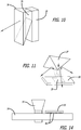
- FIG. 1 shows a wire 5, where a metal whisker 15 is extending from the wire 5.
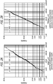
- FIGS. 2A and 2B feature graphical representations of example data illustrating whisker occurrence on a sample. (Source: Panashchenko, L., Evaluation of Environmental Tests for Tin Whisker Assessment, p. 86, Figures 59 and 60).
- JP2006291276 discloses a whisker prevention method, and device therefor.
- a metal terminal applied with a tinning on its surface is irradiated with laser beams, and only the surface layer of the tinning is melted, thereby preventing the occurrence of whiskers.
- the carrying velocity lies within the range from 1.7 to 50 mm/sec when the power density of the laser light L is 150 W/mm 2
- the carrying velocity lies within 1,300 mm/sec when the power density is 1,800 W/mm 2 the generation of whiskers can be satisfactorily prevented.
- the present disclosure relates to methods, systems, and apparatus for reducing the occurrence of metal whiskers on a metal surface.
- the present disclosure teaches a method of reducing the formation of metal whiskers on a surface having whiskering metal.
- the exemplary method comprises emitting electromagnetic energy from at least one electromagnetic energy source via a radiation field in which the whiskering metal is positioned, and controlling parameters for emitting electromagnetic energy from the at least one electromagnetic energy source.
- the at least one electromagnetic energy source comprises a terahertz emitter.
- the terahertz emitter comprises a horn antenna.
- the electromagnetic field may induce alternating electric field and current at the whisker driving disrupting energy directly into the forming whisker.
- the present disclosure teaches an apparatus for applying energy to a circuit board housing.
- the exemplary apparatus comprises at least one electromagnetic energy source positioned to provide electromagnetic energy to the circuit board housing, and a controller for controlling, e.g., the duration, frequency, power level, and amplitude of the electromagnetic energy emitted from the at least one electromagnetic energy source, wherein the circuit board housing is configured to contain electronic components having a whiskering metal.
- the at least one electromagnetic energy source comprises a terahertz emitter.
- the terahertz emitter comprises a horn antenna.
- the at least one electromagnetic energy source comprises multiple electromagnetic energy sources coupled to circuit board cards associated with the circuit board housing.
- the methods and apparatus disclosed herein reduce the occurrence of metal whiskers on metal surfaces, and in particular in electronic soldering joints in various applications.
- one or more sources of electromagnetic energy may direct electromagnetic energy to the solder joint, containing e.g. tin, to reduce the occurrence of whiskering in the solder joint.
- the electromagnetic field may be of an amplitude large enough to disrupt the physical and chemical drivers that lead to whisker growth, and even to decrease the whisker length itself by means of tip melting via resonant energy transfer to the whisker.
- the one or more sources of electromagnetic energy is configured to create a radiation field in which the whiskering metal is positioned. The energy is emitted according to controlled parameters, which may include duration of energy exposure, energy level, and the frequency of the emitted energy.
- the invention in one or more aspects thereof, relates to methods and apparatus for exposing electronic components containing tin or other whiskering metals in solder joints to electromagnetic energy that reduces the occurrence of whiskering in the solder joints, wherein the exposure occurs based on specified parameters.
- one or more sources of electromagnetic energy may be used to emit electromagnetic energy in a volume containing electronic components with solder joints having the whiskering metal.
- whiskering metals include tin, zinc, cadmium, gold, and others to varying degrees, as well as alloys of the aforementioned materials, the specification will refer primarily herein to tin as the whiskering metal for purposes of illustration only.
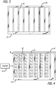
- FIG. 3 illustrates a structural frame 20, which includes an electronic bus 25 and which houses a plurality of electronic assemblies, such as circuit board cards 30.
- circuit board cards typically have a number of electronic components having tin solder joints.
- tin whiskers may form on, around, or between the tin solder joints.
- a source of electromagnetic energy may be applied to the solder joints.
- an emitter of electromagnetic radiation such as a terahertz (THz) emitter 35 is used to emit radiofrequency (RF) energy to which the solder joints are exposed.
- RF radiofrequency
- mmWaves millimeter-waves
- THz RF waves have electromagnetic wavelengths that cause resonance in whiskers of typical lengths found in tin solder (refer to FIG. 2A again).
- infrared and ultraviolet emitters may be used depending on the scale of the budding whisker formation, and the specific absorption means of disrupting the chemical or physical processes driving whisker formation.
- EM electromagnetic
- the interaction of the EM field with the metal surface within the characteristic skin depth causes disruption of the coherent stresses and chemical diffusion that result in whiskering.
- This disruption will be preferentially at the points of the nanostructures of nascent whiskers that are resonant with, e.g., the infrared EM wavelength.
- Such nascent whiskers may have lengths between, e.g., about 1 micron and 100 microns.
- the parameters of RF energy emission can be controlled to help optimize performance in reducing the occurrence of tin whiskers in the various stages of development on the solder joints. Mature (i.e.
- whiskers will be mitigated by lower frequency EM energy, such as millimeter waves and THz RF waves, and the method benefits from the electric field enhancements at the tips of such structures. Immature (i.e. smaller) whiskers will be mitigated by higher frequency EM energy, such as infrared, optical, and ultraviolet frequencies.
- the mitigation is in the form of very localized surface heating, sufficient to overcome driving internal stresses, and in the form of disruption of coherent electrical potential basis present in the material.
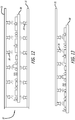
- FIG. 4 shows the structural frame 20 with multiple terahertz (THz) emitters 35 coupled to each of the circuit board cards 30. While FIG. 4 shows multiple terahertz (THz) emitters 35 coupled to each card 30, in other embodiments, each card 30 may only have one emitter 35 coupled to the card 30. In another embodiment, only one or more selected cards 30, instead of all of the cards, may have one or more emitters 35 coupled to each card 30. These cards may be part of a stand-alone apparatus to "clean" electronics from whiskers. Such an apparatus may be built into a stand-alone housing that provides a short-duration "de-whiskering" function, or alternatively, it may be built into an otherwise-standard card-bus housing.
- THz terahertz
- At least one card may each include at least one emitter 35 in parallel to the primary functions of these electronic circuit cards, for the purpose of a long duration "de-whiskering" of the cards themselves and/or the neighboring electronic cards.
- the emitters emit RF energy at specified parameters that will be explained in further detail below.
- the emitters 35 are positioned on the card 30 to emit RF energy toward an adjacent card 30.
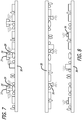
- FIG. 5 provides an example illustration of the emitters 35 emitting RF energy to adjacent circuit board cards 30.
- the structure of the THz emitter 35 is shown.
- the emitter 35 features a horn or pyramid antenna 40 for the emission of RF energy.
- the emitter 35 may include a quantum cascade laser (QCL) 45 for creating THz radiation at low temperatures in a space environment, or in a highly cooled application.
- QCL quantum cascade laser
- the emitter 35 additionally features a cooler 50, such as a Peltier cooler, to help regulate temperature control and ensure operating efficiency of the QCL 45.
- THz emitter devices may also be used that would be inherently broadband to resonate over a wide variety of whisker lengths.
- THz devices with inherently low energy may require high repetition rates of RF energy emission to achieve the necessary output power for metal whisker reduction.
- the emitter 35 is embedded within the circuit board card 30.
- the emitter 35 may be positioned on a surface of the circuit board card 30 or in some other contact with the card 30.
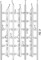
- the emitter 35 may not be placed in contact with one of the circuit board cards 30, but rather is positioned near one or more of the cards 30 in a manner that still exposes the surrounding cards 30 to sufficient THz radiation (refer to, e.g., FIG. 8 ).
- the emitters 35 may be built into the electronic components 27 having soldered connections 29 with the circuit board (refer to FIG. 7 ). The emitters are oriented to directly expose the target electronic components on the circuit board card 30 to the RF energy.
- at least one board or plate 31 of emitters 35 is formed and positioned next to at least one circuit board card 30 (refer to FIG. 9 ).
- a reflector 36 may also be positioned near the emitters 35 to reflect the RF energy in a target direction to maximize exposure of the RF energy at the target site of electronic components.
- the reflector 36 may be any that is standard practice in the art to control the direction of RF or EM energy propagation.
- the exemplary reflector 36 may be configured as a horn, surrounding the emitter 35 and mounted on a circuit board 30, as in FIG. 10 .
- the reflector may be, e.g. a reflector 37, disposed next to the emitter 35, which is mounted on the circuit board 30.
- the reflector 37 directs the RF energy of the emitter 35 back at other components on the circuit board 30.
- one or more emitters 35 may be separate from the circuit board cards 30 or other target electronic components, wherein the emitter(s) 35 are placed near the cards 30 as desired and operated to emit RF energy (refer to FIG. 13 ). After the RF energy is emitted, the emitter(s) 35 is deactivated and/or withdrawn from the components.
- a housing 32 containing one or more emitter(s) 35 is formed, wherein a structure of electronic components, such as at least one circuit board card 30, is placed as desired (refer to FIG. 12 ). Inside the housing 32, the emitter(s) 35 emit RF energy as needed, and when complete, the structure of electronic components is removed from the container 32.
- the RF energy may be generated by the emitters 35 according to specified parameters.
- a controller 55 in electronic communication with the emitters 35 may be used to control operation of the emitters 35 based on parameters programmed in the controller 55.
- the controller 55 may be an embedded microcontroller with standard preloaded software, a timer, as well as analog and digital interfaces.
- An exemplary controller commonly used in the industry at this time is the MicroChip PIC series microcontroller, manufactured by Microchip Technology Inc., located in Chandler, Arizona.
- the controller 55 may operate on demand by an external switch, on a specified schedule, and/or when built-in circuit monitors indicate the likely presence of whiskering, such as built-in high impedance "trip-wires".
- whiskering such as built-in high impedance "trip-wires”.
- some of the closely-spaced programmable pins 56 of the controller 55 near the emitter 35 are monitored as part of the controller software program for indications of shorts with adjacent pins 56, also dedicated for the "trip-wire" purpose (refer to FIG. 14 ). The dedication of such a short indicates the existence of significant whiskering conditions.
- the controller may command the application of low power continuous electromagnetic radiation and/or high power burst power application.
- the controller may specify the application of the electromagnetic energy starting at one wavelength, and then progressively sweeping in wavelength to another final wavelength; and may specify the application of the electromagnetic energy over a simultaneous band of wavelengths.
- the controller may shift the nature of the electromagnetic energy applied. For example, early in a life of a circuit board mission, only short wavelengths may be applied (i.e. wavelengths causing resonance in any budding short whiskers), and later in the life of a circuit board mission, longer wavelengths may also be applied (i.e. wavelengths causing resonance in whiskers having excessive size).
- the RF energy is applied by the emitters 35 continuously and at a low power level.
- the emitters 35 emit RF energy according to a schedule, such as on an hourly, daily, weekly, or monthly schedule. The regular application of RF energy by the emitters 35 helps to reduce the occurrence of the tin whiskers to help ensure the long-term reliability of a system otherwise susceptible to metal whiskering.
- the emitters 35 may be configured to selectively apply RF energy as desired by a user.
- the emitters 35 may be configured to emit RF energy only at the discretion of a user.
- a user may operate the emitters 35 to emit RF energy to supplement scheduled emissions.
- the frequency of the RF energy may also be controlled.
- the RF energy may be applied at a single frequency, a discrete set of frequencies, a continuous band of frequencies simultaneously, or it may be applied in a swept band of frequencies.
- the emitters 35 may emit RF energy once a month at about one watt of THz power per square centimeter of area covered, or every eight hours at about 0.01 watt of THz power per square centimeter.
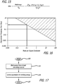
- FIG. 16 graphically represents the characteristic processing time or "melt" time, in seconds, as a function of RF power, in watts per square centimeter. This graphical illustration is presented to serve as an exemplary guideline for setting RF power and exposure time parameters, while other levels of power and time requirements may also be contemplated as known by one of ordinary skill in the art.
- FIG. 17 A summary of the process of emitting RF energy to reduce the occurrence of metal whiskers is provided in FIG. 17 .
- the process is started (block 100), and electromagnetic energy is emitted from at least one source via a radiation field wherein an electronic component with a whiskering metal is positioned (block 110).
- the parameters associated with the emission of electromagnetic energy such as the frequency and the amplitude of the electromagnetic energy, as well as the duration of its emission, are then controlled to reduce the occurrence of metal whiskers on a metal surface (block 120).
- the use of a broadband mix of frequencies (wavelengths from about 1 mm down to about 1 - 10 microns) with a power emphasis at wavelengths near 1 - 10 microns would cause resonance in budding whiskers.
- one may use a range of wavelengths from about 1 micron to about 10 microns at one power level, in parallel with a range of wavelengths from about 10 microns to about 1 mm at another power level.
- the power levels may be less than 1 Watt per square centimeter for long duration exposure (i.e. any exposure that has a total duty cycle of more than a few percent).
- the power level for a short duration exposure may be very high, up to 100 Watts per square centimeter or more.
- a short duration exposure may be 1 microsecond to 1 millisecond in duration, and a long duration exposure may be hours or days in duration.
- the process may then be ended (block 130).
- RF emitters such as those described above may be used in vehicles, aerospace equipment (e.g., critical systems such as embedded computers used for navigation, engine control, and direction as well as orientation controls, radios, transponders, and pointing and tracking electronics), communications systems, and other applications to emit RF energy to reduce the occurrence of metal whiskers in such applications.
- aerospace equipment e.g., critical systems such as embedded computers used for navigation, engine control, and direction as well as orientation controls, radios, transponders, and pointing and tracking electronics
- communications systems e.g., and other applications to emit RF energy to reduce the occurrence of metal whiskers in such applications.
Landscapes
- Engineering & Computer Science (AREA)
- Manufacturing & Machinery (AREA)
- Microelectronics & Electronic Packaging (AREA)
- Electric Connection Of Electric Components To Printed Circuits (AREA)
- Manufacturing Of Printed Wiring (AREA)
- Crystals, And After-Treatments Of Crystals (AREA)
Applications Claiming Priority (2)
| Application Number | Priority Date | Filing Date | Title |
|---|---|---|---|
| US13/656,293 US9532463B2 (en) | 2012-10-19 | 2012-10-19 | Methods and apparatus for reducing the occurrence of metal whiskers |
| PCT/US2013/057489 WO2014062301A1 (en) | 2012-10-19 | 2013-08-30 | Methods and apparatus for reducing the occurrence of metal whiskers |
Publications (2)
| Publication Number | Publication Date |
|---|---|
| EP2910094A1 EP2910094A1 (en) | 2015-08-26 |
| EP2910094B1 true EP2910094B1 (en) | 2018-08-01 |
Family
ID=49263427
Family Applications (1)
| Application Number | Title | Priority Date | Filing Date |
|---|---|---|---|
| EP13770727.9A Active EP2910094B1 (en) | 2012-10-19 | 2013-08-30 | Methods and apparatus for reducing the occurrence of metal whiskers |
Country Status (4)
| Country | Link |
|---|---|
| US (1) | US9532463B2 (enExample) |
| EP (1) | EP2910094B1 (enExample) |
| JP (1) | JP6203855B2 (enExample) |
| WO (1) | WO2014062301A1 (enExample) |
Families Citing this family (3)
| Publication number | Priority date | Publication date | Assignee | Title |
|---|---|---|---|---|
| DE102014116537B4 (de) * | 2014-11-12 | 2024-05-29 | Infineon Technologies Ag | Funktionales Hautpflaster sowie System zum Überwachen eines Körpergesundheitsparameters |
| KR102277371B1 (ko) * | 2019-03-26 | 2021-07-14 | (주)앨트론 | 위스커 성장 방지를 위한 전자빔 조사 방법 |
| CN110512244B (zh) * | 2019-09-19 | 2021-03-09 | 昆山一鼎工业科技有限公司 | 电镀雾锡产品的表面处理方法 |
Family Cites Families (15)
| Publication number | Priority date | Publication date | Assignee | Title |
|---|---|---|---|---|
| WO2008048214A2 (en) * | 2005-07-19 | 2008-04-24 | The Trustees Of Dartmouth College | Free electron pumped terahertz laser with double grating horn arrangement for collimated free wave emission |
| GB0307096D0 (en) * | 2003-03-27 | 2003-04-30 | Univ Cambridge Tech | Terahertz radiation sources and methods |
| JP2006196323A (ja) * | 2005-01-14 | 2006-07-27 | Takamatsu Mekki:Kk | 接続端子およびその製造方法 |
| JP2006216474A (ja) * | 2005-02-07 | 2006-08-17 | Sony Chem Corp | 配線体、電子機器、配線体の製造方法、および電子機器の製造方法 |
| JP4654741B2 (ja) | 2005-04-08 | 2011-03-23 | 澁谷工業株式会社 | ウィスカ防止方法 |
| JP2007090354A (ja) * | 2005-09-26 | 2007-04-12 | Fuji Xerox Co Ltd | 電気回路装置 |
| JP2007297668A (ja) * | 2006-04-28 | 2007-11-15 | Om Sangyo Kk | メッキ製品の製造方法 |
| US20070275262A1 (en) | 2006-05-23 | 2007-11-29 | Dechao Lin | Reducing formation of tin whiskers on a tin plating layer |
| US7848835B2 (en) * | 2006-06-02 | 2010-12-07 | Cymer, Inc. | High power laser flat panel workpiece treatment system controller |
| US8617913B2 (en) * | 2006-08-23 | 2013-12-31 | Rockwell Collins, Inc. | Alkali silicate glass based coating and method for applying |
| JP4986141B2 (ja) | 2007-05-08 | 2012-07-25 | 国立大学法人秋田大学 | 錫メッキの針状ウィスカの発生を抑制する方法 |
| US8071931B2 (en) * | 2007-11-13 | 2011-12-06 | Battelle Energy Alliance, Llc | Structures, systems and methods for harvesting energy from electromagnetic radiation |
| JP5388324B2 (ja) * | 2008-02-22 | 2014-01-15 | 日本圧着端子製造株式会社 | めっき層の熱処理方法 |
| JP2010256254A (ja) * | 2009-04-27 | 2010-11-11 | Panasonic Corp | 電磁波検出装置、それを備えた加熱装置および冷凍装置 |
| JP2011198683A (ja) * | 2010-03-23 | 2011-10-06 | Mitsubishi Materials Corp | コネクタ用接続端子及びその製造方法 |
-
2012
- 2012-10-19 US US13/656,293 patent/US9532463B2/en active Active
-
2013
- 2013-08-30 JP JP2015537703A patent/JP6203855B2/ja active Active
- 2013-08-30 EP EP13770727.9A patent/EP2910094B1/en active Active
- 2013-08-30 WO PCT/US2013/057489 patent/WO2014062301A1/en not_active Ceased
Also Published As
| Publication number | Publication date |
|---|---|
| WO2014062301A1 (en) | 2014-04-24 |
| EP2910094A1 (en) | 2015-08-26 |
| JP2015534279A (ja) | 2015-11-26 |
| US20140110402A1 (en) | 2014-04-24 |
| US9532463B2 (en) | 2016-12-27 |
| JP6203855B2 (ja) | 2017-09-27 |
Similar Documents
| Publication | Publication Date | Title |
|---|---|---|
| US8309885B2 (en) | Pulse temporal programmable ultrafast burst mode laser for micromachining | |
| US11980967B2 (en) | Laser micromachining with tailored bursts of short laser pulses | |
| WO1991012050A1 (en) | Probe, and method of use thereof for biomudulation of tissue, nerve and immune systems | |
| EP2910094B1 (en) | Methods and apparatus for reducing the occurrence of metal whiskers | |
| US20130164506A1 (en) | Apparatus for the selective separation of two layers of material using an ultrashort pulse source of electromagnetic radiation | |
| JP6220775B2 (ja) | ピコ秒レーザパルスを用いた高いパルス繰り返し周波数でのレーザダイレクトアブレーション | |
| JP2012516391A5 (enExample) | ||
| KR20120116948A (ko) | 일련의 레이저 펄스를 사용하여 박막에 라인을 스크라이빙하는 방법 및 장치 | |
| KR20220016855A (ko) | 레이저 가공 장치, 이를 작동하기 위한 방법, 및 이를 사용하여 피가공물을 가공하는 방법 | |
| EP3140853A1 (en) | Pulsed-mode direct-write laser metallization | |
| US10622244B2 (en) | Pulsed-mode direct-write laser metallization | |
| Nakamura et al. | Synthesis of various sized ZnO microspheres by laser ablation and their lasing characteristics | |
| Meir et al. | The localized microwave-heating (LMH) paradigm–theory, experiments, and applications | |
| CN107004454B (zh) | 用于制造电加热装置的层的接触区的方法及用于机动车的电加热装置的设备 | |
| WO1999040591A1 (en) | Passive resistive component surface ablation trimming technique using q-switched, solid-state ultraviolet wavelength laser | |
| DE102015107180A1 (de) | Verfahren zum Herstellen einer Lötverbindung, elektrischer Steckverbinder zum Verlöten mit einem Koaxialkabel und Verwendung eines solchen Steckverbinders | |
| WO1984002867A1 (en) | Method of laser soldering | |
| KR20150043193A (ko) | 테라헤르츠 연속파 발생/검출용 포토 믹서 및 그 제조 방법 | |
| Bahrami et al. | Arbitrary pulse shaping using nonuniform spacetime modulation | |
| Haun | Laser applications | |
| US20230197920A1 (en) | Manufacturing battery electrodes | |
| Glynn et al. | Reflow Soldering of Fine-pitch devices using a Nd: Yag laser | |
| Aleksandrov et al. | Plasma parameters of a nonself-sustained microwave discharge created by a programmed pulse | |
| JP2006305403A (ja) | 機能性膜パターン形成装置、機能性膜パターン形成方法及び電子機器 | |
| Lanin et al. | SOLDERING CONNECTIONS FORMATION AT INFLUENCE OF ENERGY OF ELECTROMAGNETIC FIELDS IN WIDE FREQUENCY BAND |
Legal Events
| Date | Code | Title | Description |
|---|---|---|---|
| PUAI | Public reference made under article 153(3) epc to a published international application that has entered the european phase |
Free format text: ORIGINAL CODE: 0009012 |
|
| 17P | Request for examination filed |
Effective date: 20150416 |
|
| AK | Designated contracting states |
Kind code of ref document: A1 Designated state(s): AL AT BE BG CH CY CZ DE DK EE ES FI FR GB GR HR HU IE IS IT LI LT LU LV MC MK MT NL NO PL PT RO RS SE SI SK SM TR |
|
| AX | Request for extension of the european patent |
Extension state: BA ME |
|
| DAX | Request for extension of the european patent (deleted) | ||
| GRAP | Despatch of communication of intention to grant a patent |
Free format text: ORIGINAL CODE: EPIDOSNIGR1 |
|
| INTG | Intention to grant announced |
Effective date: 20180209 |
|
| GRAJ | Information related to disapproval of communication of intention to grant by the applicant or resumption of examination proceedings by the epo deleted |
Free format text: ORIGINAL CODE: EPIDOSDIGR1 |
|
| GRAJ | Information related to disapproval of communication of intention to grant by the applicant or resumption of examination proceedings by the epo deleted |
Free format text: ORIGINAL CODE: EPIDOSDIGR1 |
|
| GRAP | Despatch of communication of intention to grant a patent |
Free format text: ORIGINAL CODE: EPIDOSNIGR1 |
|
| GRAS | Grant fee paid |
Free format text: ORIGINAL CODE: EPIDOSNIGR3 |
|
| GRAR | Information related to intention to grant a patent recorded |
Free format text: ORIGINAL CODE: EPIDOSNIGR71 |
|
| GRAS | Grant fee paid |
Free format text: ORIGINAL CODE: EPIDOSNIGR3 |
|
| INTC | Intention to grant announced (deleted) | ||
| GRAA | (expected) grant |
Free format text: ORIGINAL CODE: 0009210 |
|
| INTG | Intention to grant announced |
Effective date: 20180620 |
|
| AK | Designated contracting states |
Kind code of ref document: B1 Designated state(s): AL AT BE BG CH CY CZ DE DK EE ES FI FR GB GR HR HU IE IS IT LI LT LU LV MC MK MT NL NO PL PT RO RS SE SI SK SM TR |
|
| REG | Reference to a national code |
Ref country code: GB Ref legal event code: FG4D |
|
| REG | Reference to a national code |
Ref country code: CH Ref legal event code: EP Ref country code: AT Ref legal event code: REF Ref document number: 1025906 Country of ref document: AT Kind code of ref document: T Effective date: 20180815 |
|
| REG | Reference to a national code |
Ref country code: IE Ref legal event code: FG4D |
|
| REG | Reference to a national code |
Ref country code: FR Ref legal event code: PLFP Year of fee payment: 6 |
|
| REG | Reference to a national code |
Ref country code: DE Ref legal event code: R096 Ref document number: 602013041240 Country of ref document: DE |
|
| REG | Reference to a national code |
Ref country code: NL Ref legal event code: MP Effective date: 20180801 |
|
| REG | Reference to a national code |
Ref country code: LT Ref legal event code: MG4D |
|
| REG | Reference to a national code |
Ref country code: AT Ref legal event code: MK05 Ref document number: 1025906 Country of ref document: AT Kind code of ref document: T Effective date: 20180801 |
|
| PG25 | Lapsed in a contracting state [announced via postgrant information from national office to epo] |
Ref country code: GR Free format text: LAPSE BECAUSE OF FAILURE TO SUBMIT A TRANSLATION OF THE DESCRIPTION OR TO PAY THE FEE WITHIN THE PRESCRIBED TIME-LIMIT Effective date: 20181102 Ref country code: NO Free format text: LAPSE BECAUSE OF FAILURE TO SUBMIT A TRANSLATION OF THE DESCRIPTION OR TO PAY THE FEE WITHIN THE PRESCRIBED TIME-LIMIT Effective date: 20181101 Ref country code: AT Free format text: LAPSE BECAUSE OF FAILURE TO SUBMIT A TRANSLATION OF THE DESCRIPTION OR TO PAY THE FEE WITHIN THE PRESCRIBED TIME-LIMIT Effective date: 20180801 Ref country code: NL Free format text: LAPSE BECAUSE OF FAILURE TO SUBMIT A TRANSLATION OF THE DESCRIPTION OR TO PAY THE FEE WITHIN THE PRESCRIBED TIME-LIMIT Effective date: 20180801 Ref country code: LT Free format text: LAPSE BECAUSE OF FAILURE TO SUBMIT A TRANSLATION OF THE DESCRIPTION OR TO PAY THE FEE WITHIN THE PRESCRIBED TIME-LIMIT Effective date: 20180801 Ref country code: BG Free format text: LAPSE BECAUSE OF FAILURE TO SUBMIT A TRANSLATION OF THE DESCRIPTION OR TO PAY THE FEE WITHIN THE PRESCRIBED TIME-LIMIT Effective date: 20181101 Ref country code: IS Free format text: LAPSE BECAUSE OF FAILURE TO SUBMIT A TRANSLATION OF THE DESCRIPTION OR TO PAY THE FEE WITHIN THE PRESCRIBED TIME-LIMIT Effective date: 20181201 Ref country code: PL Free format text: LAPSE BECAUSE OF FAILURE TO SUBMIT A TRANSLATION OF THE DESCRIPTION OR TO PAY THE FEE WITHIN THE PRESCRIBED TIME-LIMIT Effective date: 20180801 Ref country code: SE Free format text: LAPSE BECAUSE OF FAILURE TO SUBMIT A TRANSLATION OF THE DESCRIPTION OR TO PAY THE FEE WITHIN THE PRESCRIBED TIME-LIMIT Effective date: 20180801 Ref country code: RS Free format text: LAPSE BECAUSE OF FAILURE TO SUBMIT A TRANSLATION OF THE DESCRIPTION OR TO PAY THE FEE WITHIN THE PRESCRIBED TIME-LIMIT Effective date: 20180801 Ref country code: FI Free format text: LAPSE BECAUSE OF FAILURE TO SUBMIT A TRANSLATION OF THE DESCRIPTION OR TO PAY THE FEE WITHIN THE PRESCRIBED TIME-LIMIT Effective date: 20180801 |
|
| PG25 | Lapsed in a contracting state [announced via postgrant information from national office to epo] |
Ref country code: AL Free format text: LAPSE BECAUSE OF FAILURE TO SUBMIT A TRANSLATION OF THE DESCRIPTION OR TO PAY THE FEE WITHIN THE PRESCRIBED TIME-LIMIT Effective date: 20180801 Ref country code: LV Free format text: LAPSE BECAUSE OF FAILURE TO SUBMIT A TRANSLATION OF THE DESCRIPTION OR TO PAY THE FEE WITHIN THE PRESCRIBED TIME-LIMIT Effective date: 20180801 Ref country code: HR Free format text: LAPSE BECAUSE OF FAILURE TO SUBMIT A TRANSLATION OF THE DESCRIPTION OR TO PAY THE FEE WITHIN THE PRESCRIBED TIME-LIMIT Effective date: 20180801 |
|
| REG | Reference to a national code |
Ref country code: CH Ref legal event code: PL |
|
| PG25 | Lapsed in a contracting state [announced via postgrant information from national office to epo] |
Ref country code: LU Free format text: LAPSE BECAUSE OF NON-PAYMENT OF DUE FEES Effective date: 20180830 Ref country code: CH Free format text: LAPSE BECAUSE OF NON-PAYMENT OF DUE FEES Effective date: 20180831 Ref country code: EE Free format text: LAPSE BECAUSE OF FAILURE TO SUBMIT A TRANSLATION OF THE DESCRIPTION OR TO PAY THE FEE WITHIN THE PRESCRIBED TIME-LIMIT Effective date: 20180801 Ref country code: LI Free format text: LAPSE BECAUSE OF NON-PAYMENT OF DUE FEES Effective date: 20180831 Ref country code: MC Free format text: LAPSE BECAUSE OF FAILURE TO SUBMIT A TRANSLATION OF THE DESCRIPTION OR TO PAY THE FEE WITHIN THE PRESCRIBED TIME-LIMIT Effective date: 20180801 Ref country code: IT Free format text: LAPSE BECAUSE OF FAILURE TO SUBMIT A TRANSLATION OF THE DESCRIPTION OR TO PAY THE FEE WITHIN THE PRESCRIBED TIME-LIMIT Effective date: 20180801 Ref country code: RO Free format text: LAPSE BECAUSE OF FAILURE TO SUBMIT A TRANSLATION OF THE DESCRIPTION OR TO PAY THE FEE WITHIN THE PRESCRIBED TIME-LIMIT Effective date: 20180801 Ref country code: CZ Free format text: LAPSE BECAUSE OF FAILURE TO SUBMIT A TRANSLATION OF THE DESCRIPTION OR TO PAY THE FEE WITHIN THE PRESCRIBED TIME-LIMIT Effective date: 20180801 Ref country code: ES Free format text: LAPSE BECAUSE OF FAILURE TO SUBMIT A TRANSLATION OF THE DESCRIPTION OR TO PAY THE FEE WITHIN THE PRESCRIBED TIME-LIMIT Effective date: 20180801 |
|
| REG | Reference to a national code |
Ref country code: DE Ref legal event code: R097 Ref document number: 602013041240 Country of ref document: DE |
|
| REG | Reference to a national code |
Ref country code: BE Ref legal event code: MM Effective date: 20180831 |
|
| PG25 | Lapsed in a contracting state [announced via postgrant information from national office to epo] |
Ref country code: SK Free format text: LAPSE BECAUSE OF FAILURE TO SUBMIT A TRANSLATION OF THE DESCRIPTION OR TO PAY THE FEE WITHIN THE PRESCRIBED TIME-LIMIT Effective date: 20180801 Ref country code: SM Free format text: LAPSE BECAUSE OF FAILURE TO SUBMIT A TRANSLATION OF THE DESCRIPTION OR TO PAY THE FEE WITHIN THE PRESCRIBED TIME-LIMIT Effective date: 20180801 Ref country code: DK Free format text: LAPSE BECAUSE OF FAILURE TO SUBMIT A TRANSLATION OF THE DESCRIPTION OR TO PAY THE FEE WITHIN THE PRESCRIBED TIME-LIMIT Effective date: 20180801 |
|
| PLBE | No opposition filed within time limit |
Free format text: ORIGINAL CODE: 0009261 |
|
| STAA | Information on the status of an ep patent application or granted ep patent |
Free format text: STATUS: NO OPPOSITION FILED WITHIN TIME LIMIT |
|
| 26N | No opposition filed |
Effective date: 20190503 |
|
| PG25 | Lapsed in a contracting state [announced via postgrant information from national office to epo] |
Ref country code: BE Free format text: LAPSE BECAUSE OF NON-PAYMENT OF DUE FEES Effective date: 20180831 Ref country code: SI Free format text: LAPSE BECAUSE OF FAILURE TO SUBMIT A TRANSLATION OF THE DESCRIPTION OR TO PAY THE FEE WITHIN THE PRESCRIBED TIME-LIMIT Effective date: 20180801 |
|
| PG25 | Lapsed in a contracting state [announced via postgrant information from national office to epo] |
Ref country code: MT Free format text: LAPSE BECAUSE OF NON-PAYMENT OF DUE FEES Effective date: 20180830 |
|
| PG25 | Lapsed in a contracting state [announced via postgrant information from national office to epo] |
Ref country code: TR Free format text: LAPSE BECAUSE OF FAILURE TO SUBMIT A TRANSLATION OF THE DESCRIPTION OR TO PAY THE FEE WITHIN THE PRESCRIBED TIME-LIMIT Effective date: 20180801 |
|
| PG25 | Lapsed in a contracting state [announced via postgrant information from national office to epo] |
Ref country code: PT Free format text: LAPSE BECAUSE OF FAILURE TO SUBMIT A TRANSLATION OF THE DESCRIPTION OR TO PAY THE FEE WITHIN THE PRESCRIBED TIME-LIMIT Effective date: 20180801 |
|
| PG25 | Lapsed in a contracting state [announced via postgrant information from national office to epo] |
Ref country code: HU Free format text: LAPSE BECAUSE OF FAILURE TO SUBMIT A TRANSLATION OF THE DESCRIPTION OR TO PAY THE FEE WITHIN THE PRESCRIBED TIME-LIMIT; INVALID AB INITIO Effective date: 20130830 Ref country code: CY Free format text: LAPSE BECAUSE OF FAILURE TO SUBMIT A TRANSLATION OF THE DESCRIPTION OR TO PAY THE FEE WITHIN THE PRESCRIBED TIME-LIMIT Effective date: 20180801 Ref country code: IE Free format text: LAPSE BECAUSE OF NON-PAYMENT OF DUE FEES Effective date: 20180830 Ref country code: MK Free format text: LAPSE BECAUSE OF NON-PAYMENT OF DUE FEES Effective date: 20180801 |
|
| P01 | Opt-out of the competence of the unified patent court (upc) registered |
Effective date: 20230516 |
|
| PGFP | Annual fee paid to national office [announced via postgrant information from national office to epo] |
Ref country code: DE Payment date: 20250827 Year of fee payment: 13 |
|
| PGFP | Annual fee paid to national office [announced via postgrant information from national office to epo] |
Ref country code: GB Payment date: 20250827 Year of fee payment: 13 |
|
| PGFP | Annual fee paid to national office [announced via postgrant information from national office to epo] |
Ref country code: FR Payment date: 20250825 Year of fee payment: 13 |