EP2905810A1 - Lichtemittierende Vorrichtungsverpackung und Beleuchtungsvorrichtung, die die Vorrichtungsverpackung enthält - Google Patents
Lichtemittierende Vorrichtungsverpackung und Beleuchtungsvorrichtung, die die Vorrichtungsverpackung enthält Download PDFInfo
- Publication number
- EP2905810A1 EP2905810A1 EP15153889.9A EP15153889A EP2905810A1 EP 2905810 A1 EP2905810 A1 EP 2905810A1 EP 15153889 A EP15153889 A EP 15153889A EP 2905810 A1 EP2905810 A1 EP 2905810A1
- Authority
- EP
- European Patent Office
- Prior art keywords
- light emitting
- emitting device
- substrate
- device package
- length
- Prior art date
- Legal status (The legal status is an assumption and is not a legal conclusion. Google has not performed a legal analysis and makes no representation as to the accuracy of the status listed.)
- Granted
Links
Images





Classifications
-
- H—ELECTRICITY
- H10—SEMICONDUCTOR DEVICES; ELECTRIC SOLID-STATE DEVICES NOT OTHERWISE PROVIDED FOR
- H10H—INORGANIC LIGHT-EMITTING SEMICONDUCTOR DEVICES HAVING POTENTIAL BARRIERS
- H10H20/00—Individual inorganic light-emitting semiconductor devices having potential barriers, e.g. light-emitting diodes [LED]
- H10H20/80—Constructional details
- H10H20/85—Packages
- H10H20/855—Optical field-shaping means, e.g. lenses
-
- H—ELECTRICITY
- H10—SEMICONDUCTOR DEVICES; ELECTRIC SOLID-STATE DEVICES NOT OTHERWISE PROVIDED FOR
- H10H—INORGANIC LIGHT-EMITTING SEMICONDUCTOR DEVICES HAVING POTENTIAL BARRIERS
- H10H20/00—Individual inorganic light-emitting semiconductor devices having potential barriers, e.g. light-emitting diodes [LED]
- H10H20/80—Constructional details
- H10H20/81—Bodies
- H10H20/819—Bodies characterised by their shape, e.g. curved or truncated substrates
-
- H—ELECTRICITY
- H10—SEMICONDUCTOR DEVICES; ELECTRIC SOLID-STATE DEVICES NOT OTHERWISE PROVIDED FOR
- H10H—INORGANIC LIGHT-EMITTING SEMICONDUCTOR DEVICES HAVING POTENTIAL BARRIERS
- H10H29/00—Integrated devices, or assemblies of multiple devices, comprising at least one light-emitting semiconductor element covered by group H10H20/00
- H10H29/10—Integrated devices comprising at least one light-emitting semiconductor component covered by group H10H20/00
-
- H—ELECTRICITY
- H10—SEMICONDUCTOR DEVICES; ELECTRIC SOLID-STATE DEVICES NOT OTHERWISE PROVIDED FOR
- H10W—GENERIC PACKAGES, INTERCONNECTIONS, CONNECTORS OR OTHER CONSTRUCTIONAL DETAILS OF DEVICES COVERED BY CLASS H10
- H10W90/00—Package configurations
Definitions
- the present invention relates to a light emitting device package and a lighting apparatus including the same.
- a light emitting device such as a light emitting diode (LED) is a type of a semiconductor device that converts electric energy into optical energy through a P-N junction structure of a compound semiconductor, has a small power consumption and long life, and is capable of miniaturization and weight reduction, and thereby has been spotlighted as the next generation light source of a lighting apparatus.
- LED light emitting diode
- a blue LED and an ultraviolet (UV) LED that use nitrides having excellent physical and chemical characteristics have been introduced. Since the blue LED or UV LED may implement white light or other monochromatic lights using a phosphor material, application fields of the LED are expanding.
- a linear lighting device may be configured using such a light emitting device, and in this instance, in order to reduce the number of required light emitting devices, light emitted from the light emitting device should be more widely diffused in a specific direction.
- an anisotropic lens may be mounted, but there are difficulties in anisotropically designing and manufacturing the lens, and optical efficiency is degraded when such a lens is adopted.
- the present invention is directed to a light emitting device package which may obtain an anisotropic illumination distribution while applying an isotropic lens which can be easily designed and manufactured, and a light apparatus including the same.
- a light emitting device package including: a light emitting device that has a first side extending in a first direction and a second side extending in a second direction, and is disposed on a substrate; and a molding unit that has a shape of an isotropic lens disposed on the substrate to surround the light emitting device, wherein a square root of ⁇ (length of the first side) 2 + (length of the second side) 2 ⁇ is smaller than a diameter of the isotropic lens, and the length of the first side is at least 5/3 times more than the length of the second side.
- the isotropic lens may have an aspherical surface shape with its center recessed.
- a plurality of the light emitting devices may be arranged in the first direction and the second direction.
- the number of the light emitting devices arranged in the first direction may be at least 5/3 times more than the number of the light emitting devices arranged in the second direction.
- first direction and the second direction may intersect each other.
- a light emitting device package including: a substrate; a light emitting device that is disposed on the substrate and electrically connected to the substrate; and a molding unit that is disposed on the substrate to surround the light emitting device, wherein an upper surface of the light emitting device includes two first sides parallel to each other and two second sides parallel to each other that intersect the first sides, and the first sides are formed longer than the second sides.
- first side and the second side may vertically intersect each other, and a length of the first side may be at least 5/3 times more than a length of the second side.
- the light emitting device may include a plurality of light emitting device units.
- the number of the light emitting device units arranged in a direction of the first side may be at least 5/3 times more than the number of the light emitting device units arranged in a direction of the second side.
- the molding unit may be an aspherical lens.
- a lighting apparatus including: at least one light emitting device package, wherein the light emitting device package includes a substrate, a light emitting device that is disposed on the substrate and electrically connected to the substrate, and a molding unit that is disposed on the substrate to surround the light emitting device, and wherein an upper surface of the light emitting device includes two first sides parallel to each other and two second sides parallel to each other that intersect the first sides, and the first sides are formed longer than the second sides.
- first side and the second side may vertically intersect each other, and a length of the first side is at least 5/3 times more than a length of the second side.
- a plurality of the light emitting device packages may be provided, and arranged in a row.
- Example embodiments of the present invention are disclosed herein. Also, specific structural and functional details disclosed herein are merely representative for purposes of describing the example embodiments of the present invention. However, the example embodiments of the present invention may be embodied in many alternate forms and should not be construed as limited to example embodiments of the present invention set forth herein.
- FIG. 1 is a perspective view showing a light emitting device package according to a first comparative example
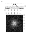
- FIG. 2 is a view showing an illumination distribution of the device shown in FIG. 1
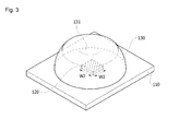
- FIG. 3 is a perspective view showing a light emitting device package according to a second comparative example
- FIG. 4 is a view showing an illumination distribution of the device shown in FIG. 3
- the unit of the numerical values shown in FIGS. 2 and 4 is mm
- X and Y respectively indicate a first direction and a second direction intersecting the first direction.
- the light emitting device package according to the first and second comparative examples may include a light emitting device 120 that is disposed on a substrate 110, and a molding unit 130 that has a shape of an isotropic lens disposed on the substrate 110 to surround the light emitting device 120.
- the molding unit 130 may have an aspherical surface shape with a concave portion 131 recessed at the center thereof, and a planar shape of the light emitting device 120 according to the first and second comparative examples may be a square shape.
- the light emitting device 120 according to the first comparative example may have a first width W1 and the light emitting device 120 according to the second comparative example may have a second width W2 relatively smaller than the first width W1.
- an illumination distribution may be changed depending on the size of the light emitting device 120. Specifically, it can be seen that light emitted from the light emitting device 120 having the second width W2 relatively smaller than the first width W1 is more widely diffused. However, when the planar shape of the light emitting device 120 is the square shape regardless of the size of the light emitting device 120, the light emitted from the light emitting device 120 is isotropically diffused, such as with a circular shape.
- an anisotropic secondary lens may be mounted.
- FIG. 5 is a perspective view showing a light emitting device package according to a first embodiment of the present invention
- FIG. 6 is a view showing an illumination distribution of the device shown in FIG. 5
- the unit of the numerical values shown in FIG. 6 is mm
- X and Y respectively indicate a first direction and a second direction intersecting the first direction.
- the light emitting device package may include a light emitting device 120 that is disposed on a substrate 110, and a molding unit that has a shape of an isotropic lens disposed on the substrate 110 to surround the light emitting device 120.
- a planar shape of the light emitting device 120 is a rectangular shape having a long axis W1 and a short axis W2, and a diagonal length of the light emitting device 120 should be smaller than a diameter D of the molding unit 130 so that the molding unit 130 can surround the light emitting device 120 (see, Equation 1).
- the substrate 110 may be a typical printed circuit board (PCB) or a lead frame, and formed of at least one material of alumina, quartz, zirconia, forsterite, cordierite, beryllia, mullite, calcium zirconate, silicon carbide, aluminum nitride, fused silica, low temperature co-fired ceramic (LTCC), plastic, graphite, and a metal.
- PCB printed circuit board
- a lead frame formed of at least one material of alumina, quartz, zirconia, forsterite, cordierite, beryllia, mullite, calcium zirconate, silicon carbide, aluminum nitride, fused silica, low temperature co-fired ceramic (LTCC), plastic, graphite, and a metal.
- PCB printed circuit board
- the light emitting device 120 may be a device that emits light by recombination of minority carriers (electrons or electron holes) injected using a P-N junction structure of a compound semiconductor, and may be a light emitting diode (LED). Although not shown in the present drawing, the light emitting device 120 may be electrically connected to an electrode of the substrate 110 through a wire or the like so that power may be applied to the light emitting device 120, and when the light emitted from the light emitting device 120 is blue light, the light emitting device 120 may include a yellow-based phosphor that converts the blue light into white light.
- the long axis W1 of the light emitting device 120 should be longer than the short axis W2 thereof by at least 5/3 times or more, and the anisotropy of the illumination distribution may be increased by increasing a ratio (W1/W2) of the long axis and the short axis of the light emitting device 120.
- the molding unit 130 is a lens-integrated type package having the function of a lens while protecting the light emitting device 120, and may have an aspherical surface shape with the concave portion 131 recessed at the center thereof, and therefore it is possible to increase a directional angle of the light emitted from the light emitting device 120. Meanwhile, since the light emitted from the light emitting device 120 should be transmitted to the outside, the molding unit 130 may be formed of transparent resin such as silicon resin or epoxy resin, and a dispersant or a phosphor may be added inside the molding unit 130 according to need.
- the light emitting device package according to the first embodiment of the present invention may obtain the anisotropic illumination distribution by applying the molding unit 130 having the shape of the isotropic lens which can be easily designed and manufactured. Specifically, the light emitted from the light emitting device 120 is more widely diffused in a direction of the short axis W2 rather than in the direction of the long axis W1, and thereby an oval-shaped light distribution appears. Meanwhile, in order to control the light distribution in the direction of the long axis W1 when the molding unit 130 is designed, the light distribution of the square-shaped light emitting device 120 having the first width W1 as shown in the first comparative example may be utilized. Similarly, in order to control the light distribution in the direction of the short axis W2, the light distribution of the square-shaped light emitting device 120 having the second width W2 as shown in the second comparative example may be utilized.
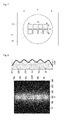
- FIG. 7 is a plan view showing a light emitting device package according to a second embodiment of the present invention.
- the description of the present embodiment detailed description of substantially the same part as that of the above-described first embodiment will be omitted.
- the light emitting device package according to the second embodiment of the present invention may include a plurality of light emitting devices 120 that are arranged on the substrate 110 so as to have a rectangular shape having the long axis W1 and the short axis W2, and the isotropic lens-shaped molding unit 130 that is disposed on the substrate 110 to surround the plurality of light emitting devices 120.
- a planar shape of each of the light emitting devices 120 may be a square shape or a rectangular shape, and a diagonal length of the rectangular shape formed by arranging the plurality of light emitting devices 120 should be smaller than the diameter D of the molding unit 130 so that the molding unit 130 can surround the whole of the plurality of light emitting devices 120 (see, Equation 1).
- the substrate 110 may be a typical PCB or a lead frame, and formed of a material such as that of the first embodiment.
- the light emitting device 120 is a device that emits light such as an LED.
- the number of the light emitting devices 120 arranged in the direction of the long axis W1 should be larger than the number of the light emitting devices 120 arranged in the direction of the short axis W2 by at least 5/3 times or more.
- the molding unit 130 may be a lens-integrated type package having the function of a lens while protecting the light emitting device 120, have an aspherical surface shape with its center recessed, and be formed of transparent resin such as silicon resin or epoxy resin.
- FIGS. 8 and 9 are views showing an illumination distribution of a linear lighting apparatus configured of a light emitting device package according to a comparative example
- FIG. 10 is a view showing an illumination distribution of a linear lighting apparatus configured of a light emitting device package according to an embodiment of the present invention.
- the unit of the numerical values shown in FIGS. 8 to 10 is mm
- X and Y respectively indicate a first direction and a second direction intersecting the first direction.
- a linear lighting apparatus may be configured by arranging a plurality of light emitting device packages that are point light sources in a row.
- the light emitting device package including the square-shaped light emitting device according to a comparative example may have an isotropic illumination distribution, and therefore the number of the light emitting device packages required in a configuration of the linear lighting apparatus is relatively large.
- the linear lighting apparatus is configured by arranging the light emitting device packages including the square-shaped light emitting device according to a comparative example in a row, when the number of the light emitting device packages in the linear lighting apparatus of FIG. 8 is reduced by half, each of the light emitting device packages is visually recognized as a point light source rather than as a linear light source.
- each of the light emitting device packages may be visually recognized as the linear light source although the number of the light emitting device packages is reduced in the same manner as in a linear lighting module of FIG. 9 .
- the light emitting device may be formed into a rectangular shape or a plurality of light emitting devices may be arranged in a rectangular shape, and therefore an anisotropic illumination distribution may be obtained while applying an isotropic lens which can be easily designed and manufactured, thereby reducing manufacturing time and costs while increasing optical efficiency.
Landscapes
- Non-Portable Lighting Devices Or Systems Thereof (AREA)
- Led Device Packages (AREA)
- Fastening Of Light Sources Or Lamp Holders (AREA)
Abstract
Description
- The present invention relates to a light emitting device package and a lighting apparatus including the same.
- A light emitting device such as a light emitting diode (LED) is a type of a semiconductor device that converts electric energy into optical energy through a P-N junction structure of a compound semiconductor, has a small power consumption and long life, and is capable of miniaturization and weight reduction, and thereby has been spotlighted as the next generation light source of a lighting apparatus. In recent years, a blue LED and an ultraviolet (UV) LED that use nitrides having excellent physical and chemical characteristics have been introduced. Since the blue LED or UV LED may implement white light or other monochromatic lights using a phosphor material, application fields of the LED are expanding.
- A linear lighting device may be configured using such a light emitting device, and in this instance, in order to reduce the number of required light emitting devices, light emitted from the light emitting device should be more widely diffused in a specific direction. In this manner, in order to obtain an anisotropic light distribution, an anisotropic lens may be mounted, but there are difficulties in anisotropically designing and manufacturing the lens, and optical efficiency is degraded when such a lens is adopted.
- The present invention is directed to a light emitting device package which may obtain an anisotropic illumination distribution while applying an isotropic lens which can be easily designed and manufactured, and a light apparatus including the same.
- According to an aspect of the present invention, there is provided a light emitting device package including: a light emitting device that has a first side extending in a first direction and a second side extending in a second direction, and is disposed on a substrate; and a molding unit that has a shape of an isotropic lens disposed on the substrate to surround the light emitting device, wherein a square root of {(length of the first side) 2 + (length of the second side) 2} is smaller than a diameter of the isotropic lens, and the length of the first side is at least 5/3 times more than the length of the second side.
- Here, the isotropic lens may have an aspherical surface shape with its center recessed.
- Also, a plurality of the light emitting devices may be arranged in the first direction and the second direction.
- Also, the number of the light emitting devices arranged in the first direction may be at least 5/3 times more than the number of the light emitting devices arranged in the second direction.
- Also, the first direction and the second direction may intersect each other.
- According to another aspect of the present invention, there is provided a light emitting device package including: a substrate; a light emitting device that is disposed on the substrate and electrically connected to the substrate; and a molding unit that is disposed on the substrate to surround the light emitting device, wherein an upper surface of the light emitting device includes two first sides parallel to each other and two second sides parallel to each other that intersect the first sides, and the first sides are formed longer than the second sides.
- Here, the first side and the second side may vertically intersect each other, and a length of the first side may be at least 5/3 times more than a length of the second side.
- Also, the light emitting device may include a plurality of light emitting device units.
- Also, the number of the light emitting device units arranged in a direction of the first side may be at least 5/3 times more than the number of the light emitting device units arranged in a direction of the second side.
- Also, the molding unit may be an aspherical lens.
- According to still another aspect of the present invention, there is provided a lighting apparatus including: at least one light emitting device package, wherein the light emitting device package includes a substrate, a light emitting device that is disposed on the substrate and electrically connected to the substrate, and a molding unit that is disposed on the substrate to surround the light emitting device, and wherein an upper surface of the light emitting device includes two first sides parallel to each other and two second sides parallel to each other that intersect the first sides, and the first sides are formed longer than the second sides.
- Here, the first side and the second side may vertically intersect each other, and a length of the first side is at least 5/3 times more than a length of the second side.
- Also, a plurality of the light emitting device packages may be provided, and arranged in a row.
- The above and other objects, features and advantages of the present invention will become more apparent to those of ordinary skill in the art by describing in detail exemplary embodiments thereof with reference to the accompanying drawings, in which:
-
FIG. 1 is a perspective view showing a light emitting device package according to a first comparative example; -
FIG. 2 is a view showing an illumination distribution of the device shown inFIG. 1 ; -
FIG. 3 is a perspective view showing a light emitting device package according to a second comparative example; -
FIG. 4 is a view showing an illumination distribution of the device shown inFIG. 3 ; -
FIG. 5 is a perspective view showing a light emitting device package according to a first embodiment of the present invention; -
FIG. 6 is a view showing an illumination distribution of the device shown inFIG. 5 ; -
FIG. 7 is a plan view showing a light emitting device package according to a second embodiment of the present invention; -
FIGS. 8 and9 are views showing an illumination distribution of a linear lighting apparatus configured of a light emitting device package according to a comparative example; and -
FIG. 10 is a view showing an illumination distribution of a linear lighting apparatus configured of a light emitting device package according to an embodiment of the present invention. - Example embodiments of the present invention are disclosed herein. Also, specific structural and functional details disclosed herein are merely representative for purposes of describing the example embodiments of the present invention. However, the example embodiments of the present invention may be embodied in many alternate forms and should not be construed as limited to example embodiments of the present invention set forth herein.
- Unless otherwise defined, all terms (including technical and scientific terms) used herein have the same meaning as commonly understood by one of ordinary skill in the art to which this invention belongs. It will be further understood that terms, such as those defined in commonly used dictionaries, should be interpreted as having a meaning that is consistent with their meaning in the context of the relevant art and will not be interpreted in an idealized or overly formal sense unless expressly so defined herein.
- It will be understood that when an element is referred to as being "connected" or "coupled" to another element, it can be directly connected or coupled to the other element or intervening elements may be present. In contrast, when an element is referred to as being "directly connected" or "directly coupled" to another element, there are no intervening elements present.
- The terminology used herein is for the purpose of describing particular embodiments only and is not intended to be limiting of the invention. As used herein, the singular forms "a", "an" and "the" are intended to include the plural forms as well, unless the context clearly indicates otherwise. It will be further understood that the terms "comprises", "comprising,", "includes" and/or "including", when used herein, specify the presence of stated features, integers, steps, operations, elements, and/or components, but do not preclude the presence or addition of one or more other features, integers, steps, operations, elements, components, and/or groups thereof.
- Accordingly, while the invention is susceptible to various modifications and alternative forms, specific embodiments thereof are shown by way of example in the drawings and will herein be described in detail. It should be understood, however, that there is no intent to limit the invention to the particular forms disclosed, but on the contrary, the invention is to cover all modifications, equivalents, and alternatives falling within the spirit and scope of the invention. Like numbers refer to like elements throughout the description of the figures.
-
FIG. 1 is a perspective view showing a light emitting device package according to a first comparative example,FIG. 2 is a view showing an illumination distribution of the device shown inFIG. 1 ,FIG. 3 is a perspective view showing a light emitting device package according to a second comparative example, andFIG. 4 is a view showing an illumination distribution of the device shown inFIG. 3 . Here, the unit of the numerical values shown inFIGS. 2 and4 is mm, and X and Y respectively indicate a first direction and a second direction intersecting the first direction. - Referring to
FIGS. 1 and3 , the light emitting device package according to the first and second comparative examples may include alight emitting device 120 that is disposed on asubstrate 110, and amolding unit 130 that has a shape of an isotropic lens disposed on thesubstrate 110 to surround thelight emitting device 120. Themolding unit 130 may have an aspherical surface shape with aconcave portion 131 recessed at the center thereof, and a planar shape of thelight emitting device 120 according to the first and second comparative examples may be a square shape. As shown in the drawings, thelight emitting device 120 according to the first comparative example may have a first width W1 and thelight emitting device 120 according to the second comparative example may have a second width W2 relatively smaller than the first width W1. - Referring to
FIGS. 2 and4 , when themolding units 130 according to the first and second comparative examples have the same shape and size, an illumination distribution may be changed depending on the size of thelight emitting device 120. Specifically, it can be seen that light emitted from thelight emitting device 120 having the second width W2 relatively smaller than the first width W1 is more widely diffused. However, when the planar shape of thelight emitting device 120 is the square shape regardless of the size of thelight emitting device 120, the light emitted from thelight emitting device 120 is isotropically diffused, such as with a circular shape. - Meanwhile, in a linear lighting apparatus or the like, light is required to be more widely diffused in a specific direction, and in order to obtain such an illumination distribution, an anisotropic secondary lens may be mounted. However, it is not easy to design the anisotropic secondary lens, and manufacturing time and costs may be increased while optical efficiency is degraded when the anisotropic secondary lens is applied to a product.
-
FIG. 5 is a perspective view showing a light emitting device package according to a first embodiment of the present invention, andFIG. 6 is a view showing an illumination distribution of the device shown inFIG. 5 . Here, the unit of the numerical values shown inFIG. 6 is mm, and X and Y respectively indicate a first direction and a second direction intersecting the first direction. - Referring to
FIG. 5 , the light emitting device package according to the first embodiment of the present invention may include alight emitting device 120 that is disposed on asubstrate 110, and a molding unit that has a shape of an isotropic lens disposed on thesubstrate 110 to surround thelight emitting device 120. A planar shape of thelight emitting device 120 is a rectangular shape having a long axis W1 and a short axis W2, and a diagonal length of thelight emitting device 120 should be smaller than a diameter D of themolding unit 130 so that themolding unit 130 can surround the light emitting device 120 (see, Equation 1).
- The
substrate 110 may be a typical printed circuit board (PCB) or a lead frame, and formed of at least one material of alumina, quartz, zirconia, forsterite, cordierite, beryllia, mullite, calcium zirconate, silicon carbide, aluminum nitride, fused silica, low temperature co-fired ceramic (LTCC), plastic, graphite, and a metal. - The
light emitting device 120 may be a device that emits light by recombination of minority carriers (electrons or electron holes) injected using a P-N junction structure of a compound semiconductor, and may be a light emitting diode (LED). Although not shown in the present drawing, thelight emitting device 120 may be electrically connected to an electrode of thesubstrate 110 through a wire or the like so that power may be applied to thelight emitting device 120, and when the light emitted from thelight emitting device 120 is blue light, thelight emitting device 120 may include a yellow-based phosphor that converts the blue light into white light. In particular, in order to obtain an anisotropic illumination distribution required for a configuration of the linear lighting apparatus, the long axis W1 of thelight emitting device 120 should be longer than the short axis W2 thereof by at least 5/3 times or more, and the anisotropy of the illumination distribution may be increased by increasing a ratio (W1/W2) of the long axis and the short axis of thelight emitting device 120. - The
molding unit 130 is a lens-integrated type package having the function of a lens while protecting thelight emitting device 120, and may have an aspherical surface shape with theconcave portion 131 recessed at the center thereof, and therefore it is possible to increase a directional angle of the light emitted from thelight emitting device 120. Meanwhile, since the light emitted from thelight emitting device 120 should be transmitted to the outside, themolding unit 130 may be formed of transparent resin such as silicon resin or epoxy resin, and a dispersant or a phosphor may be added inside themolding unit 130 according to need. - Referring to
FIG. 6 , the light emitting device package according to the first embodiment of the present invention may obtain the anisotropic illumination distribution by applying themolding unit 130 having the shape of the isotropic lens which can be easily designed and manufactured. Specifically, the light emitted from thelight emitting device 120 is more widely diffused in a direction of the short axis W2 rather than in the direction of the long axis W1, and thereby an oval-shaped light distribution appears. Meanwhile, in order to control the light distribution in the direction of the long axis W1 when themolding unit 130 is designed, the light distribution of the square-shapedlight emitting device 120 having the first width W1 as shown in the first comparative example may be utilized. Similarly, in order to control the light distribution in the direction of the short axis W2, the light distribution of the square-shapedlight emitting device 120 having the second width W2 as shown in the second comparative example may be utilized. -
FIG. 7 is a plan view showing a light emitting device package according to a second embodiment of the present invention. In the description of the present embodiment, detailed description of substantially the same part as that of the above-described first embodiment will be omitted. - Referring to
FIG. 7 , the light emitting device package according to the second embodiment of the present invention may include a plurality of light emittingdevices 120 that are arranged on thesubstrate 110 so as to have a rectangular shape having the long axis W1 and the short axis W2, and the isotropic lens-shapedmolding unit 130 that is disposed on thesubstrate 110 to surround the plurality of light emittingdevices 120. A planar shape of each of thelight emitting devices 120 may be a square shape or a rectangular shape, and a diagonal length of the rectangular shape formed by arranging the plurality of light emittingdevices 120 should be smaller than the diameter D of themolding unit 130 so that themolding unit 130 can surround the whole of the plurality of light emitting devices 120 (see, Equation 1). - The
substrate 110 may be a typical PCB or a lead frame, and formed of a material such as that of the first embodiment. In addition, thelight emitting device 120 is a device that emits light such as an LED. When each of thelight emitting devices 120 has a square shape and the same size, in order to obtain an anisotropic illumination distribution required for a configuration of the linear lighting apparatus, the number of thelight emitting devices 120 arranged in the direction of the long axis W1 should be larger than the number of thelight emitting devices 120 arranged in the direction of the short axis W2 by at least 5/3 times or more. Meanwhile, themolding unit 130 may be a lens-integrated type package having the function of a lens while protecting thelight emitting device 120, have an aspherical surface shape with its center recessed, and be formed of transparent resin such as silicon resin or epoxy resin. -
FIGS. 8 and9 are views showing an illumination distribution of a linear lighting apparatus configured of a light emitting device package according to a comparative example, andFIG. 10 is a view showing an illumination distribution of a linear lighting apparatus configured of a light emitting device package according to an embodiment of the present invention. Here, the unit of the numerical values shown inFIGS. 8 to 10 is mm, and X and Y respectively indicate a first direction and a second direction intersecting the first direction. - Referring to
FIG. 8 , a linear lighting apparatus may be configured by arranging a plurality of light emitting device packages that are point light sources in a row. The light emitting device package including the square-shaped light emitting device according to a comparative example may have an isotropic illumination distribution, and therefore the number of the light emitting device packages required in a configuration of the linear lighting apparatus is relatively large. - Referring to
FIG. 9 , in a case in which the linear lighting apparatus is configured by arranging the light emitting device packages including the square-shaped light emitting device according to a comparative example in a row, when the number of the light emitting device packages in the linear lighting apparatus ofFIG. 8 is reduced by half, each of the light emitting device packages is visually recognized as a point light source rather than as a linear light source. - Referring to
FIG. 10 , in a case in which the linear lighting apparatus is configured by arranging the plurality of light emitting device packages according to an embodiment of the present invention in a row, by arranging the light emitting device packages in the direction of the short axis in a row, in which the light emitted from the light emitting device package is widely diffused, each of the light emitting device packages may be visually recognized as the linear light source although the number of the light emitting device packages is reduced in the same manner as in a linear lighting module ofFIG. 9 . - As described above, according to the light emitting device package and the light apparatus including the same according to the embodiments of the present invention, the light emitting device may be formed into a rectangular shape or a plurality of light emitting devices may be arranged in a rectangular shape, and therefore an anisotropic illumination distribution may be obtained while applying an isotropic lens which can be easily designed and manufactured, thereby reducing manufacturing time and costs while increasing optical efficiency.
- It will be apparent to those skilled in the art that various modifications can be made to the above-described exemplary embodiments of the present invention without departing from the spirit or scope of the invention. Thus, it is intended that the present invention covers all such modifications provided they come within the scope of the appended claims and their equivalents.
Claims (13)
- A light emitting device package comprising:a light emitting device(120) that has a first side extending in a first direction and a second side extending in a second direction, and is disposed on a substrate(110); anda molding unit(130) that has a shape of an isotropic lens disposed on the substrate(110) to surround the light emitting device(120),wherein a square root of {(length of the first side) 2 + (length of the second side) 2} is smaller than a diameter of the isotropic lens, and the length of the first side is at least 5/3 times more than the length of the second side.
- The light emitting device package of claim 1, wherein the isotropic lens has an aspherical surface shape with its center recessed.
- The light emitting device package of claim 1, wherein a plurality of the light emitting devices(120) are arranged in the first direction and the second direction.
- The light emitting device package of claim 3, wherein the number of the light emitting devices(120) arranged in the first direction is at least 5/3 times more than the number of the light emitting devices(120) arranged in the second direction.
- The light emitting device package of claim 1, wherein the first direction and the second direction intersect each other.
- A light emitting device package comprising:a substrate(110);a light emitting device(120) that is disposed on the substrate and electrically connected to the substrate(110); anda molding unit(130) that is disposed on the substrate(110) to surround the light emitting device(120),wherein an upper surface of the light emitting device(120) includes two first sides parallel to each other and two second sides parallel to each other that intersect the first sides, and the first sides are formed longer than the second sides.
- The light emitting device package of claim 6, wherein the first side and the second side vertically intersect each other, and a length of the first side is at least 5/3 times more than a length of the second side.
- The light emitting device package of claim 6, wherein the light emitting device(120) includes a plurality of light emitting device units.
- The light emitting device package of claim 8, wherein the number of the light emitting device units arranged in a direction of the first side is at least 5/3 times more than the number of the light emitting device units arranged in a direction of the second side.
- The light emitting device package of claim 6, wherein the molding unit(130) is an aspherical lens.
- A lighting apparatus comprising
at least one light emitting device package,
wherein the light emitting device package includes
a substrate(110),
a light emitting device(120) that is disposed on the substrate(110) and electrically connected to the substrate(110), and
a molding unit(130) that is disposed on the substrate(110) to surround the light emitting device(120), and
wherein an upper surface of the light emitting device(120) includes two first sides parallel to each other and two second sides parallel to each other that intersect the first sides, and the first sides are formed longer than the second sides. - The lighting apparatus of claim 11, wherein the first side and the second side vertically intersect each other, and a length of the first side is at least 5/3 times more than a length of the second side.
- The lighting apparatus of claim 11, wherein a plurality of the light emitting device packages are provided, and arranged in a row.
Applications Claiming Priority (1)
| Application Number | Priority Date | Filing Date | Title |
|---|---|---|---|
| KR1020140013148A KR102154061B1 (en) | 2014-02-05 | 2014-02-05 | Light emitting device package and lighting apparatus including the same |
Publications (2)
| Publication Number | Publication Date |
|---|---|
| EP2905810A1 true EP2905810A1 (en) | 2015-08-12 |
| EP2905810B1 EP2905810B1 (en) | 2019-08-14 |
Family
ID=52444208
Family Applications (1)
| Application Number | Title | Priority Date | Filing Date |
|---|---|---|---|
| EP15153889.9A Active EP2905810B1 (en) | 2014-02-05 | 2015-02-05 | Light emitting device package |
Country Status (4)
| Country | Link |
|---|---|
| US (1) | US20150221839A1 (en) |
| EP (1) | EP2905810B1 (en) |
| KR (1) | KR102154061B1 (en) |
| CN (1) | CN104821361A (en) |
Families Citing this family (5)
| Publication number | Priority date | Publication date | Assignee | Title |
|---|---|---|---|---|
| JP2017067633A (en) * | 2015-09-30 | 2017-04-06 | キヤノン株式会社 | Checkup apparatus, and manufacturing method |
| KR101667902B1 (en) * | 2016-04-25 | 2016-10-20 | 한국광기술원 | Lighting module with rectangular light source |
| US10069098B2 (en) | 2016-06-29 | 2018-09-04 | Lg Display Co., Ltd. | Organic light emitting display device, method of manufacturing the same, and head mounted display including the same |
| USD996378S1 (en) * | 2022-03-09 | 2023-08-22 | Creeled, Inc. | Light-emitting diode package |
| US12355013B2 (en) | 2022-04-21 | 2025-07-08 | Creeled, Inc. | Emission height arrangements in light-emitting diode packages and related devices and methods |
Citations (4)
| Publication number | Priority date | Publication date | Assignee | Title |
|---|---|---|---|---|
| US20110291131A1 (en) * | 2009-02-19 | 2011-12-01 | Shin Ito | Light emitting device, planar light source, and display device |
| US20120069545A1 (en) * | 2010-11-08 | 2012-03-22 | Lg Innotek Co., Ltd. | Lighting device |
| US20120068198A1 (en) * | 2010-09-20 | 2012-03-22 | Cree, Inc. | High density multi-chip led devices |
| US20130141920A1 (en) * | 2011-12-06 | 2013-06-06 | Cree, Inc. | Light emitter devices and methods with reduced dimensions and improved light output |
Family Cites Families (8)
| Publication number | Priority date | Publication date | Assignee | Title |
|---|---|---|---|---|
| WO2006080729A1 (en) * | 2004-10-07 | 2006-08-03 | Seoul Semiconductor Co., Ltd. | Side illumination lens and luminescent device using the same |
| US8748915B2 (en) | 2006-04-24 | 2014-06-10 | Cree Hong Kong Limited | Emitter package with angled or vertical LED |
| JPWO2008096714A1 (en) * | 2007-02-05 | 2010-05-20 | 株式会社ニコン | Resin-sealed light emitting device, planar light source, method for producing the same, and liquid crystal display device |
| JP4999551B2 (en) * | 2007-05-24 | 2012-08-15 | 株式会社小糸製作所 | Light emitting element module |
| US9666762B2 (en) | 2007-10-31 | 2017-05-30 | Cree, Inc. | Multi-chip light emitter packages and related methods |
| JP2011165833A (en) | 2010-02-08 | 2011-08-25 | Toshiba Corp | Led module |
| KR101708025B1 (en) * | 2010-08-19 | 2017-02-20 | 서울반도체 주식회사 | Lens and light-emitting device having the same |
| US8652860B2 (en) * | 2011-01-09 | 2014-02-18 | Bridgelux, Inc. | Packaging photon building blocks having only top side connections in a molded interconnect structure |
-
2014
- 2014-02-05 KR KR1020140013148A patent/KR102154061B1/en not_active Expired - Fee Related
-
2015
- 2015-02-04 US US14/614,121 patent/US20150221839A1/en not_active Abandoned
- 2015-02-05 CN CN201510061833.3A patent/CN104821361A/en active Pending
- 2015-02-05 EP EP15153889.9A patent/EP2905810B1/en active Active
Patent Citations (4)
| Publication number | Priority date | Publication date | Assignee | Title |
|---|---|---|---|---|
| US20110291131A1 (en) * | 2009-02-19 | 2011-12-01 | Shin Ito | Light emitting device, planar light source, and display device |
| US20120068198A1 (en) * | 2010-09-20 | 2012-03-22 | Cree, Inc. | High density multi-chip led devices |
| US20120069545A1 (en) * | 2010-11-08 | 2012-03-22 | Lg Innotek Co., Ltd. | Lighting device |
| US20130141920A1 (en) * | 2011-12-06 | 2013-06-06 | Cree, Inc. | Light emitter devices and methods with reduced dimensions and improved light output |
Also Published As
| Publication number | Publication date |
|---|---|
| KR20150092596A (en) | 2015-08-13 |
| KR102154061B1 (en) | 2020-09-09 |
| EP2905810B1 (en) | 2019-08-14 |
| US20150221839A1 (en) | 2015-08-06 |
| CN104821361A (en) | 2015-08-05 |
Similar Documents
| Publication | Publication Date | Title |
|---|---|---|
| US9897266B2 (en) | Light source module and lighting apparatus including the same | |
| EP2905810B1 (en) | Light emitting device package | |
| US9203006B2 (en) | Light emitting device | |
| JP6616088B2 (en) | LED assembly and LED bulb using the LED assembly | |
| US9997684B2 (en) | Pre-rotated overmoulded bidirectional spreading lens for stretched leadframe architecture | |
| EP2743999A2 (en) | Light emitting device package including phosphor film, method of manufacturing the same, and lighting apparatus using the same | |
| CN105627111B (en) | Light emitting module and lighting device including the same | |
| KR101644140B1 (en) | Led lens having an asymmetric orientation angle pattern and light emitting device having the same | |
| KR20140129749A (en) | Light source unit and display device having the same | |
| KR101653395B1 (en) | Multichip LED package | |
| US20130039064A1 (en) | Light emitting diode bulb | |
| CN113574312A (en) | Light emitting device | |
| KR20090032867A (en) | Directional conversion lens and light emitting device for backlight including the same | |
| US20150221620A1 (en) | Light emitting device package and lighting apparatus including the same | |
| KR100705552B1 (en) | Light emitting diode | |
| KR20130085735A (en) | Lighting device | |
| KR102140226B1 (en) | Light emitting device package and lighting apparatus including the same | |
| KR101274486B1 (en) | LED Lighting Apparatus with free form moudule and method of preparing the same | |
| KR102437786B1 (en) | Lighting module using light emitting diode package | |
| KR20140063922A (en) | Led lighting device | |
| US20150116999A1 (en) | Mono-axial lens for multiple light sources | |
| KR102029867B1 (en) | Light emitting device package, and lighting system | |
| KR20160068062A (en) | Lighting Apparatus having LED module and Fresnel lens | |
| CN104747975A (en) | Laser diode light source device and backlight module thereof | |
| KR20110109409A (en) | LED lens and light emitting device including the same |
Legal Events
| Date | Code | Title | Description |
|---|---|---|---|
| PUAI | Public reference made under article 153(3) epc to a published international application that has entered the european phase |
Free format text: ORIGINAL CODE: 0009012 |
|
| AK | Designated contracting states |
Kind code of ref document: A1 Designated state(s): AL AT BE BG CH CY CZ DE DK EE ES FI FR GB GR HR HU IE IS IT LI LT LU LV MC MK MT NL NO PL PT RO RS SE SI SK SM TR |
|
| AX | Request for extension of the european patent |
Extension state: BA ME |
|
| 17P | Request for examination filed |
Effective date: 20160209 |
|
| RBV | Designated contracting states (corrected) |
Designated state(s): AL AT BE BG CH CY CZ DE DK EE ES FI FR GB GR HR HU IE IS IT LI LT LU LV MC MK MT NL NO PL PT RO RS SE SI SK SM TR |
|
| RAP1 | Party data changed (applicant data changed or rights of an application transferred) |
Owner name: LG INNOTEK CO., LTD. |
|
| STAA | Information on the status of an ep patent application or granted ep patent |
Free format text: STATUS: EXAMINATION IS IN PROGRESS |
|
| 17Q | First examination report despatched |
Effective date: 20180612 |
|
| REG | Reference to a national code |
Ref country code: DE Ref legal event code: R079 Ref document number: 602015035662 Country of ref document: DE Free format text: PREVIOUS MAIN CLASS: H01L0027150000 Ipc: H01L0033200000 |
|
| GRAP | Despatch of communication of intention to grant a patent |
Free format text: ORIGINAL CODE: EPIDOSNIGR1 |
|
| STAA | Information on the status of an ep patent application or granted ep patent |
Free format text: STATUS: GRANT OF PATENT IS INTENDED |
|
| RIC1 | Information provided on ipc code assigned before grant |
Ipc: H01L 33/20 20100101AFI20190214BHEP Ipc: H01L 25/075 20060101ALN20190214BHEP Ipc: H01L 33/58 20100101ALI20190214BHEP |
|
| INTG | Intention to grant announced |
Effective date: 20190311 |
|
| GRAS | Grant fee paid |
Free format text: ORIGINAL CODE: EPIDOSNIGR3 |
|
| GRAA | (expected) grant |
Free format text: ORIGINAL CODE: 0009210 |
|
| STAA | Information on the status of an ep patent application or granted ep patent |
Free format text: STATUS: THE PATENT HAS BEEN GRANTED |
|
| AK | Designated contracting states |
Kind code of ref document: B1 Designated state(s): AL AT BE BG CH CY CZ DE DK EE ES FI FR GB GR HR HU IE IS IT LI LT LU LV MC MK MT NL NO PL PT RO RS SE SI SK SM TR |
|
| REG | Reference to a national code |
Ref country code: GB Ref legal event code: FG4D |
|
| REG | Reference to a national code |
Ref country code: CH Ref legal event code: EP Ref country code: AT Ref legal event code: REF Ref document number: 1168057 Country of ref document: AT Kind code of ref document: T Effective date: 20190815 |
|
| REG | Reference to a national code |
Ref country code: IE Ref legal event code: FG4D |
|
| REG | Reference to a national code |
Ref country code: DE Ref legal event code: R096 Ref document number: 602015035662 Country of ref document: DE |
|
| REG | Reference to a national code |
Ref country code: NL Ref legal event code: MP Effective date: 20190814 |
|
| REG | Reference to a national code |
Ref country code: LT Ref legal event code: MG4D |
|
| PG25 | Lapsed in a contracting state [announced via postgrant information from national office to epo] |
Ref country code: FI Free format text: LAPSE BECAUSE OF FAILURE TO SUBMIT A TRANSLATION OF THE DESCRIPTION OR TO PAY THE FEE WITHIN THE PRESCRIBED TIME-LIMIT Effective date: 20190814 Ref country code: HR Free format text: LAPSE BECAUSE OF FAILURE TO SUBMIT A TRANSLATION OF THE DESCRIPTION OR TO PAY THE FEE WITHIN THE PRESCRIBED TIME-LIMIT Effective date: 20190814 Ref country code: SE Free format text: LAPSE BECAUSE OF FAILURE TO SUBMIT A TRANSLATION OF THE DESCRIPTION OR TO PAY THE FEE WITHIN THE PRESCRIBED TIME-LIMIT Effective date: 20190814 Ref country code: NO Free format text: LAPSE BECAUSE OF FAILURE TO SUBMIT A TRANSLATION OF THE DESCRIPTION OR TO PAY THE FEE WITHIN THE PRESCRIBED TIME-LIMIT Effective date: 20191114 Ref country code: PT Free format text: LAPSE BECAUSE OF FAILURE TO SUBMIT A TRANSLATION OF THE DESCRIPTION OR TO PAY THE FEE WITHIN THE PRESCRIBED TIME-LIMIT Effective date: 20191216 Ref country code: LT Free format text: LAPSE BECAUSE OF FAILURE TO SUBMIT A TRANSLATION OF THE DESCRIPTION OR TO PAY THE FEE WITHIN THE PRESCRIBED TIME-LIMIT Effective date: 20190814 Ref country code: NL Free format text: LAPSE BECAUSE OF FAILURE TO SUBMIT A TRANSLATION OF THE DESCRIPTION OR TO PAY THE FEE WITHIN THE PRESCRIBED TIME-LIMIT Effective date: 20190814 Ref country code: BG Free format text: LAPSE BECAUSE OF FAILURE TO SUBMIT A TRANSLATION OF THE DESCRIPTION OR TO PAY THE FEE WITHIN THE PRESCRIBED TIME-LIMIT Effective date: 20191114 |
|
| REG | Reference to a national code |
Ref country code: AT Ref legal event code: MK05 Ref document number: 1168057 Country of ref document: AT Kind code of ref document: T Effective date: 20190814 |
|
| PG25 | Lapsed in a contracting state [announced via postgrant information from national office to epo] |
Ref country code: ES Free format text: LAPSE BECAUSE OF FAILURE TO SUBMIT A TRANSLATION OF THE DESCRIPTION OR TO PAY THE FEE WITHIN THE PRESCRIBED TIME-LIMIT Effective date: 20190814 Ref country code: GR Free format text: LAPSE BECAUSE OF FAILURE TO SUBMIT A TRANSLATION OF THE DESCRIPTION OR TO PAY THE FEE WITHIN THE PRESCRIBED TIME-LIMIT Effective date: 20191115 Ref country code: LV Free format text: LAPSE BECAUSE OF FAILURE TO SUBMIT A TRANSLATION OF THE DESCRIPTION OR TO PAY THE FEE WITHIN THE PRESCRIBED TIME-LIMIT Effective date: 20190814 Ref country code: AL Free format text: LAPSE BECAUSE OF FAILURE TO SUBMIT A TRANSLATION OF THE DESCRIPTION OR TO PAY THE FEE WITHIN THE PRESCRIBED TIME-LIMIT Effective date: 20190814 Ref country code: RS Free format text: LAPSE BECAUSE OF FAILURE TO SUBMIT A TRANSLATION OF THE DESCRIPTION OR TO PAY THE FEE WITHIN THE PRESCRIBED TIME-LIMIT Effective date: 20190814 Ref country code: IS Free format text: LAPSE BECAUSE OF FAILURE TO SUBMIT A TRANSLATION OF THE DESCRIPTION OR TO PAY THE FEE WITHIN THE PRESCRIBED TIME-LIMIT Effective date: 20191214 |
|
| PG25 | Lapsed in a contracting state [announced via postgrant information from national office to epo] |
Ref country code: TR Free format text: LAPSE BECAUSE OF FAILURE TO SUBMIT A TRANSLATION OF THE DESCRIPTION OR TO PAY THE FEE WITHIN THE PRESCRIBED TIME-LIMIT Effective date: 20190814 |
|
| PG25 | Lapsed in a contracting state [announced via postgrant information from national office to epo] |
Ref country code: PL Free format text: LAPSE BECAUSE OF FAILURE TO SUBMIT A TRANSLATION OF THE DESCRIPTION OR TO PAY THE FEE WITHIN THE PRESCRIBED TIME-LIMIT Effective date: 20190814 Ref country code: EE Free format text: LAPSE BECAUSE OF FAILURE TO SUBMIT A TRANSLATION OF THE DESCRIPTION OR TO PAY THE FEE WITHIN THE PRESCRIBED TIME-LIMIT Effective date: 20190814 Ref country code: AT Free format text: LAPSE BECAUSE OF FAILURE TO SUBMIT A TRANSLATION OF THE DESCRIPTION OR TO PAY THE FEE WITHIN THE PRESCRIBED TIME-LIMIT Effective date: 20190814 Ref country code: RO Free format text: LAPSE BECAUSE OF FAILURE TO SUBMIT A TRANSLATION OF THE DESCRIPTION OR TO PAY THE FEE WITHIN THE PRESCRIBED TIME-LIMIT Effective date: 20190814 Ref country code: IT Free format text: LAPSE BECAUSE OF FAILURE TO SUBMIT A TRANSLATION OF THE DESCRIPTION OR TO PAY THE FEE WITHIN THE PRESCRIBED TIME-LIMIT Effective date: 20190814 Ref country code: DK Free format text: LAPSE BECAUSE OF FAILURE TO SUBMIT A TRANSLATION OF THE DESCRIPTION OR TO PAY THE FEE WITHIN THE PRESCRIBED TIME-LIMIT Effective date: 20190814 |
|
| PG25 | Lapsed in a contracting state [announced via postgrant information from national office to epo] |
Ref country code: SK Free format text: LAPSE BECAUSE OF FAILURE TO SUBMIT A TRANSLATION OF THE DESCRIPTION OR TO PAY THE FEE WITHIN THE PRESCRIBED TIME-LIMIT Effective date: 20190814 Ref country code: CZ Free format text: LAPSE BECAUSE OF FAILURE TO SUBMIT A TRANSLATION OF THE DESCRIPTION OR TO PAY THE FEE WITHIN THE PRESCRIBED TIME-LIMIT Effective date: 20190814 Ref country code: IS Free format text: LAPSE BECAUSE OF FAILURE TO SUBMIT A TRANSLATION OF THE DESCRIPTION OR TO PAY THE FEE WITHIN THE PRESCRIBED TIME-LIMIT Effective date: 20200224 Ref country code: SM Free format text: LAPSE BECAUSE OF FAILURE TO SUBMIT A TRANSLATION OF THE DESCRIPTION OR TO PAY THE FEE WITHIN THE PRESCRIBED TIME-LIMIT Effective date: 20190814 |
|
| REG | Reference to a national code |
Ref country code: DE Ref legal event code: R097 Ref document number: 602015035662 Country of ref document: DE |
|
| PLBE | No opposition filed within time limit |
Free format text: ORIGINAL CODE: 0009261 |
|
| STAA | Information on the status of an ep patent application or granted ep patent |
Free format text: STATUS: NO OPPOSITION FILED WITHIN TIME LIMIT |
|
| PG2D | Information on lapse in contracting state deleted |
Ref country code: IS |
|
| 26N | No opposition filed |
Effective date: 20200603 |
|
| PG25 | Lapsed in a contracting state [announced via postgrant information from national office to epo] |
Ref country code: SI Free format text: LAPSE BECAUSE OF FAILURE TO SUBMIT A TRANSLATION OF THE DESCRIPTION OR TO PAY THE FEE WITHIN THE PRESCRIBED TIME-LIMIT Effective date: 20190814 |
|
| REG | Reference to a national code |
Ref country code: CH Ref legal event code: PL |
|
| GBPC | Gb: european patent ceased through non-payment of renewal fee |
Effective date: 20200205 |
|
| REG | Reference to a national code |
Ref country code: BE Ref legal event code: MM Effective date: 20200229 |
|
| PG25 | Lapsed in a contracting state [announced via postgrant information from national office to epo] |
Ref country code: MC Free format text: LAPSE BECAUSE OF FAILURE TO SUBMIT A TRANSLATION OF THE DESCRIPTION OR TO PAY THE FEE WITHIN THE PRESCRIBED TIME-LIMIT Effective date: 20190814 Ref country code: LU Free format text: LAPSE BECAUSE OF NON-PAYMENT OF DUE FEES Effective date: 20200205 |
|
| PG25 | Lapsed in a contracting state [announced via postgrant information from national office to epo] |
Ref country code: LI Free format text: LAPSE BECAUSE OF NON-PAYMENT OF DUE FEES Effective date: 20200229 Ref country code: CH Free format text: LAPSE BECAUSE OF NON-PAYMENT OF DUE FEES Effective date: 20200229 |
|
| PG25 | Lapsed in a contracting state [announced via postgrant information from national office to epo] |
Ref country code: GB Free format text: LAPSE BECAUSE OF NON-PAYMENT OF DUE FEES Effective date: 20200205 Ref country code: IE Free format text: LAPSE BECAUSE OF NON-PAYMENT OF DUE FEES Effective date: 20200205 |
|
| PG25 | Lapsed in a contracting state [announced via postgrant information from national office to epo] |
Ref country code: BE Free format text: LAPSE BECAUSE OF NON-PAYMENT OF DUE FEES Effective date: 20200229 |
|
| REG | Reference to a national code |
Ref country code: DE Ref legal event code: R081 Ref document number: 602015035662 Country of ref document: DE Owner name: SUZHOU LEKIN SEMICONDUCTOR CO. LTD., TAICANG, CN Free format text: FORMER OWNER: LG INNOTEK CO., LTD., SEOUL, KR |
|
| PG25 | Lapsed in a contracting state [announced via postgrant information from national office to epo] |
Ref country code: MT Free format text: LAPSE BECAUSE OF FAILURE TO SUBMIT A TRANSLATION OF THE DESCRIPTION OR TO PAY THE FEE WITHIN THE PRESCRIBED TIME-LIMIT Effective date: 20190814 Ref country code: CY Free format text: LAPSE BECAUSE OF FAILURE TO SUBMIT A TRANSLATION OF THE DESCRIPTION OR TO PAY THE FEE WITHIN THE PRESCRIBED TIME-LIMIT Effective date: 20190814 |
|
| PG25 | Lapsed in a contracting state [announced via postgrant information from national office to epo] |
Ref country code: MK Free format text: LAPSE BECAUSE OF FAILURE TO SUBMIT A TRANSLATION OF THE DESCRIPTION OR TO PAY THE FEE WITHIN THE PRESCRIBED TIME-LIMIT Effective date: 20190814 |
|
| PGFP | Annual fee paid to national office [announced via postgrant information from national office to epo] |
Ref country code: FR Payment date: 20230110 Year of fee payment: 9 |
|
| PGFP | Annual fee paid to national office [announced via postgrant information from national office to epo] |
Ref country code: DE Payment date: 20240116 Year of fee payment: 10 |
|
| REG | Reference to a national code |
Ref country code: DE Ref legal event code: R079 Ref document number: 602015035662 Country of ref document: DE Free format text: PREVIOUS MAIN CLASS: H01L0033200000 Ipc: H10H0020819000 |
|
| PG25 | Lapsed in a contracting state [announced via postgrant information from national office to epo] |
Ref country code: FR Free format text: LAPSE BECAUSE OF NON-PAYMENT OF DUE FEES Effective date: 20240229 |
|
| PG25 | Lapsed in a contracting state [announced via postgrant information from national office to epo] |
Ref country code: FR Free format text: LAPSE BECAUSE OF NON-PAYMENT OF DUE FEES Effective date: 20240229 |
|
| REG | Reference to a national code |
Ref country code: DE Ref legal event code: R119 Ref document number: 602015035662 Country of ref document: DE |
|
| PG25 | Lapsed in a contracting state [announced via postgrant information from national office to epo] |
Ref country code: DE Free format text: LAPSE BECAUSE OF NON-PAYMENT OF DUE FEES Effective date: 20250902 |