EP2904766B1 - Metallization and anodization of plastic and conductive parts of the body of an apparatus - Google Patents
Metallization and anodization of plastic and conductive parts of the body of an apparatus Download PDFInfo
- Publication number
- EP2904766B1 EP2904766B1 EP13844142.3A EP13844142A EP2904766B1 EP 2904766 B1 EP2904766 B1 EP 2904766B1 EP 13844142 A EP13844142 A EP 13844142A EP 2904766 B1 EP2904766 B1 EP 2904766B1
- Authority
- EP
- European Patent Office
- Prior art keywords
- conductive
- plastic part
- plastic
- layer
- electronic device
- Prior art date
- Legal status (The legal status is an assumption and is not a legal conclusion. Google has not performed a legal analysis and makes no representation as to the accuracy of the status listed.)
- Active
Links
Images


Classifications
-
- H—ELECTRICITY
- H04—ELECTRIC COMMUNICATION TECHNIQUE
- H04M—TELEPHONIC COMMUNICATION
- H04M1/00—Substation equipment, e.g. for use by subscribers
- H04M1/02—Constructional features of telephone sets
- H04M1/0202—Portable telephone sets, e.g. cordless phones, mobile phones or bar type handsets
- H04M1/0279—Improving the user comfort or ergonomics
- H04M1/0283—Improving the user comfort or ergonomics for providing a decorative aspect, e.g. customization of casings, exchangeable faceplate
-
- G—PHYSICS
- G06—COMPUTING OR CALCULATING; COUNTING
- G06F—ELECTRIC DIGITAL DATA PROCESSING
- G06F1/00—Details not covered by groups G06F3/00 - G06F13/00 and G06F21/00
- G06F1/16—Constructional details or arrangements
- G06F1/18—Packaging or power distribution
- G06F1/181—Enclosures
-
- H—ELECTRICITY
- H04—ELECTRIC COMMUNICATION TECHNIQUE
- H04M—TELEPHONIC COMMUNICATION
- H04M1/00—Substation equipment, e.g. for use by subscribers
- H04M1/02—Constructional features of telephone sets
- H04M1/0202—Portable telephone sets, e.g. cordless phones, mobile phones or bar type handsets
Definitions
- An example embodiment relates generally to the body of an apparatus and, more particularly, to the metallization and anodization of the plastic and conductive parts of the body of an apparatus, such as a portable electronic device.
- the body of a mobile device such as a cellular telephone, a laptop computer, a tablet computer, a personal digital assistant (PDA) or the like may include one or more metal parts and one or more plastic parts.
- a polyphenylene sulfide (PPS) part may be insert molded or overmolded to an aluminum part to form the body of a mobile device.
- PPS polyphenylene sulfide
- a mobile device may include one or more antennas disposed within the body.
- the portion of the body that is aligned with the antennas may be formed of plastic.
- the body of some mobile devices may include a portion having a complex geometry that may be difficult, costly or otherwise inefficient to fabricate from a metal.
- the portion of the body of a mobile device that has a complex geometry may also be formed of plastic.
- plastic parts within the body of a mobile device may introduce a number of issues. From an aesthetic standpoint, the plastic part may appear different than the metal part, thereby potentially reducing the attractiveness of the mobile device.
- the plastic part may form a stripe, seam or window between metal parts of the body of the mobile device. Such a seam may be undesirable in some instances in which a seamless body is aesthetically preferable.
- a body that includes a plastic part in the form of a stripe or seam may disadvantageously permit the metal parts that are physically separated by the plastic part to sometimes be inadvertently electrically connected by a user of the mobile device while carrying or holding the mobile device.
- the surface of the plastic part may be softer than the surface of the metal part with this difference in the feel of a plastic part relative to a metal part being potentially disconcerting to the user of the mobile device.
- the plastic part may be coated separate from the metal part, such as by painting or the application of a hard coating to the plastic part, prior to combination with the metal part.
- the plastic parts and the metal parts may exhibit a color difference and/or the plastic parts and the metal parts may not be perfectly aligned with one another such that there is a step or offset exists between the plastic and metal parts, thereby detracting from the aesthetic appeal of body of the mobile device.
- a non-conductive vapor metallization (NCVM) coating may be applied to the body of a mobile device having both plastic and metal parts so as to provide a metallic appearance to the plastic parts, thereby creating a more uniform appearance.
- NCVM-coated plastic parts will still have a different tactile feeling than the metal parts and, in instances in which a top coat is been applied to the NCVM-coated plastic parts, the visual appearance of the plastic parts may no longer be metallic, that is, the plastic parts may no longer have a consistent appearance with the metal parts.
- the surface hardness of an NCVM coating is less than that of metal, thereby potentially leading to increased wear of the NCVM coated plastic part which may, in turn, further increase the visual differences between the metal and plastic parts such that the resulting body of the mobile device eventually becomes less attractive.
- D1 ( US2010097276A1 ) describes a housing for electronic device includes a substrate, the substrate be formed by an integration of a metal member and a plastic member, the metal member and the plastic member cooperatively forming an outer surface of the substrate; and a decorative coating formed on the outer surface.
- a method for making the housing and an electronic device using the housing are provided.
- D2 ( WO12122300A2 ) describes anodized electroplated aluminum structures and methods for making the same.
- Cosmetic structures according to embodiments of the invention of D2 are provided by electroplating a non-cosmetic structure with aluminum and then anodizing the electroplated aluminum. This produces cosmetic structures that may possess desired structural and cosmetic properties and that may be suitable for use a housing or support members of electronic devices.
- a method of fabricating at least a portion of the body of an apparatus, such as a portable electronic device, that includes both plastic parts and conductive parts is provided in accordance with an example embodiment.
- the body of the apparatus and a portable electronic device are also provided according to example embodiments of the present invention with the body being relatively seamless such that the interface between the plastic and conductive parts is indistinguishable.
- the body that is fabricated in accordance with an example embodiment of the invention may be more aesthetically attractive while still permitting plastic parts to be incorporated within the body, such as in conjunction with an antenna or with more geometrically complex parts.
- the body that is fabricated in accordance with an example embodiment of the present invention may include plastic parts that are scratch resistant and that provide comparable tactile feedback as the conductive parts of the body.
- circuitry refers to all of the following: (a)hardware-only circuit implementations (such as implementations in only analog and/or digital circuitry) and (b) to combinations of circuits and software (and/or firmware), such as (as applicable): (i) to a combination of processor(s) or (ii) to portions of processor(s)/software (including digital signal processor(s)), software, and memory(ies) that work together to cause an apparatus, such as a mobile phone or server, to perform various functions) and (c) to circuits, such as a microprocessor(s) or a portion of a microprocessor(s), that require software or firmware for operation, even if the software or firmware is not physically present.
- circuitry applies to all uses of this term in this application, including in any claims.
- circuitry would also cover an implementation of merely a processor (or multiple processors) or portion of a processor and its (or their) accompanying software and/or firmware.
- circuitry would also cover, for example and if applicable to the particular claim element, a baseband integrated circuit or application specific integrated circuit for a mobile phone or a similar integrated circuit in server, a cellular network device, or other network device.
- Portable electronic devices such as a mobile telephone, e.g., a cellular telephone, a smartphone or the like, a personal digital assistant (PDA), a laptop computer, a tablet computer, a navigation system, a music player, a game player, computer workstation or any of numerous other computation devices, content generation devices, content consumption devices or combinations thereof, generally include a body, such as a housing, that provides strength and rigidity so as to protect electronic circuitry disposed within the housing.
- the body of a portable electronic device may also be configured to have an attractive aesthetic appearance so as to be appealing to a user.
- the body of some portable electronic devices may not be formed entirely of a conductive material, but may be formed of a combination of one or more conductive parts and one or more plastic parts.
- the body of a portable electronic device may include a plastic part for various reasons including the radio frequency (RF) transparency of the plastic part and/or the ability to more readily form complex geometrical shapes from a plastic part.
- RF radio frequency
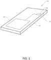
- FIG. 1 illustrates a portable electronic device 10, such as a mobile telephone, personal digital assistant (PDA) or the like, that includes a body 12, such as a housing, and electronic circuitry 14, such as one or more processors, one or more memories, etc., disposed at least partially and, more typically, entirely within the body of the portable electronic device, as represented by the dashed lines in FIG. 1 .
- the electronic circuitry disposed within the body of the portable electronic device of this embodiment may include an antenna 16 for transmitting and/or receiving signals, such as RF signals.
- the body of the portable electronic device of this embodiment may include a plastic part 18, e.g., a plastic window having a width, for example, of about 1 mm, with the antenna being aligned with the plastic parts such that signals are transmitted to and/or from the antenna through the plastic part, which is more RF transmissive than the metal parts and, in some instances, is transparent to RF signals.
- the antenna 16 is illustrated as being located at some distance from an inside surface of the body 12 of the portable electronic device 10, in other words there is a gap therebetween, this is merely an example.
- the antenna 16 may be located less than 1 mm from the inside surface of the body 12, but not touching any part of the body 12.
- the antenna 16 may be located so as to be touching the inside surface of the plastic part 18 of the body 12 where the antenna 16 is a separate part from the body 12.
- the antenna 16 may be attached to and therefore touching the inside surface of the plastic part 18 of the body 12 and thus part of the body 12.
- the antenna 17 may even be located more than 1 mm from the inside surface of the body 12.
- the antenna 16 may or may not touch the inside surface of the plastic part 18 of the body 12, but the conductive part of the antenna 16 may not touch any conductive part of the body 12.
- FIG. 2 illustrates a portable electronic device 10, such as a laptop computer, that has a body that includes a first portion 20, such as a keyboard frame, having a more complex geometry than other, e.g., second, portions 22 of the housing.
- the first portion having the more complex geometry may be formed by the plastic part
- the second portion of the housing that has the less complex geometry may be formed by the conductive part.
- the conductive part may serve to provide strength and rigidity to the housing
- the plastic part is utilized to form the portion of the housing having a more complex geometry since structures having a more complex geometry are generally easier and/or less costly to form from plastic than from metal.
- the housing may have various structures with a complex geometry including, for example, one or more screw towers, fixing elements, snap fits, undercut shapes or the like.
- the portable electronic device of the embodiment of FIG. 2 may also include electronic circuitry at least partially disposed within the body.
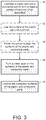
- a method of fabricating the body of an apparatus such as an electronic device and, more particularly, a portable electronic device may be provided as shown in FIG. 3 .
- one or more plastic parts and one or more conductive parts may be combined to form at least a portion of the body of the portable electronic device. See block 30 of FIG. 3 .
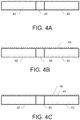
- the plastic part and the conductive part may be combined in various manners including, for example, by co-molding the plastic part 40 and the conductive parts 42 as shown, for example, in FIG. 4A .
- the plastic part may be insert molded relative to the conductive part.
- the conductive part may be overmolded with a plastic part. Regardless of the manner in which the plastic and conductive parts are combined, the combination of the plastic and conductive parts form the body.
- the plastic part 40 may be formed of various plastic materials including plastic materials that are transparent to RF signals, such as polyphenylene sulfide (PPS). Alternatively, the plastic part may be formed from polycarbonate or polyamide materials or other plastic materials.
- the conductive parts 42 may also be formed of various conductive materials including, for example, aluminum, graphite, carbon, composite materials or the like.
- the surfaces of the plastic part 40 and the conductive parts 42 may be metallized, such as by being subjected to vapor deposition or by printing of the metal thereupon, in order to form a metal layer on the surfaces of the plastic part and the conductive parts.
- the surfaces of the plastic part and the conductive parts may be subjected to physical vapor deposition (PVD), such as a PVD sputtering process, in order to vacuum metalize the surfaces of the plastic part and the conductive parts.
- PVD physical vapor deposition
- NCVM non-conductive vapor metallization
- the surfaces of the plastic part and the conductive parts may be subjected to chemical vapor deposition (CVD) in order to metalize the surfaces of the plastic part and the conductive parts.
- CVD chemical vapor deposition
- the surfaces of the plastic part and the conductive parts may be subjected to electroplating.
- the vapor deposition of one embodiment may include physical vapor deposition followed by chemical vapor deposition in order to permit the thickness of the metallization layer to be more readily tailored.
- the entire surface of the body 12 of the portable electronic device 10 including the entirety of the surfaces of the plastic and conductive parts is subjected to metallization, such as NCVM.
- metallization such as NCVM.
- the surface of the body of the portable electronic device need not be masked during the metallization, thereby increasing the efficiency of the fabrication procedure.
- a layer 44 comprised of a plurality of metal particles may be deposited upon the surfaces of the plastic and conductive parts as shown in FIG. 4B with the layer formed by metallization being transparent to RF signals.
- the layer deposited by metallization may provide a consistent metallic appearance not only to the conductive parts, but also to the plastic part.
- the layer formed by the metal particles is shown to be uniform, although the deposition of the metal particles and the corresponding layer formed by the metal particles need not be uniform and may be irregular in response to a more random deposition of the metal particles.
- the layer formed by the metallization may be comprised of various materials including, for example, aluminum.
- the metallized surfaces of the plastic and conductive parts may then be anodized.
- the entire surface of the body 12 of the portable electronic device 10 including the entirety of the surfaces of the plastic and conductive parts may be anodized such that there is also no need for masking the surface of the body of the portable electronic device during anodization, thereby further increasing the efficiency of the fabrication procedure.
- the coating 46 that is deposited by the anodization may be formed of a variety of materials, such as a non-conductive metal-oxide, e.g., aluminum oxide, or other metallic coatings, thereby reducing issues relating to short circuiting of the conductive parts 42 that form the body of the portable electronic device since the anodization coating is electrically non-conductive.
- the anodization of the body of the portable electronic device is relatively hard and provides for scratch resistance.
- the coating applied by anodization is relatively thin such that the resulting coating is transparent to signals transmitted to and from an antenna disposed within the body of the portable electronic device, such as RF signals.
- the coating formed by anodization may have a thickness of no more than 50 ⁇ m and, in one embodiment, of no more than 10 -20 ⁇ m.
- the anodization coating provides a seamless appearance even though the body is formed of both plastic and conductive parts, thereby improving the aesthetic appearance of the body of the portable electronic device.
- the coating formed by anodization may also be dyed so as to have various colors and/or may be subjected to various surface finishes to further facilitate the aesthetic appearance of the portable electronic device.
- the layer 44 formed by metallization serves to activate the surface of the plastic part 40 so as to permit anodization of the plastic part, concurrent with the anodization of the conductive parts 42.
- the layer formed by the metallization may have a thickness that is sufficiently thick in order to support or activate the surface of the plastic part for subsequent anodization, while remaining thin enough to be transparent for the signals transmitted to and/or from the antenna, such RF signals.
- the layer formed by metallization may have a thickness between 0.001 ⁇ m and 10 ⁇ m.
- the surface of the plastic part 40 may be primed prior to the metallization in order to ensure that the layer formed by the metallization adheres to the surface of the plastic part.
- the surface of the plastic part of one embodiment may be recessed relative to the surface of the conductive part 42 that is positioned adjacent to the plastic part.
- the surface of the plastic part may then be coated with a primer 48, such as ultraviolet (UV)-cured acrylates, epoxies, polyurethane-based lacquers or combination thereof, prior to subjecting the surfaces of the plastic and conductive parts to metallization, such as vapor deposition, e.g., to NCVM. See block 32 of FIG. 3 and FIG. 5B . Thereafter, the primer that has coated the surface of the plastic part may be polished so as to be aligned with the surface of the conductive part. See block 34 FIG. 3 and FIG. 5C .
- a primer 48 such as ultraviolet (UV)-cured acrylates, epoxies, polyurethane-based lacquers or combination thereof
- the surfaces of the plastic part may be subjected to metallization, such as vapor deposition, e.g., NCVM, in order to metallize the surfaces of the plastic and conductive parts. See block 36 of FIG. 3 and FIG. 5D .
- metallization such as vapor deposition, e.g., NCVM
- NCVM vapor deposition
- the metallized surfaces of the plastic and conductive parts may be anodized as also described above and as shown in block 38 of FIG. 3 and FIG. 5E .
- certain ones of the operations described in conjunction with FIG. 3 may be modified or further amplified as described below.
- additional optional operations may also be included, such as illustrated by the operations represented by blocks with dashed lines in FIG. 3 . It should be appreciated that each of the modifications, optional additions or amplifications may be included with the operations described above either alone or in combination with any others among the features described herein.
Landscapes
- Engineering & Computer Science (AREA)
- Theoretical Computer Science (AREA)
- Signal Processing (AREA)
- General Engineering & Computer Science (AREA)
- Human Computer Interaction (AREA)
- Physics & Mathematics (AREA)
- Power Engineering (AREA)
- General Physics & Mathematics (AREA)
- Computer Hardware Design (AREA)
- Casings For Electric Apparatus (AREA)
- Telephone Set Structure (AREA)
- Microelectronics & Electronic Packaging (AREA)
- Other Surface Treatments For Metallic Materials (AREA)
Description
- An example embodiment relates generally to the body of an apparatus and, more particularly, to the metallization and anodization of the plastic and conductive parts of the body of an apparatus, such as a portable electronic device.
- The body of a mobile device, such as a cellular telephone, a laptop computer, a tablet computer, a personal digital assistant (PDA) or the like may include one or more metal parts and one or more plastic parts. For example, a polyphenylene sulfide (PPS) part may be insert molded or overmolded to an aluminum part to form the body of a mobile device. Although it may be desirable to form the entire body of a mobile device from metal such that the body is both strong and has a consistent and aesthetic appearance, many mobile devices are configured in such manner as to require the body to include some combination of plastic and metal parts. For example, a mobile device may include one or more antennas disposed within the body. In order to permit the transmission of radio frequency (RF) signals to and from the antennas, the portion of the body that is aligned with the antennas may be formed of plastic. Additionally, the body of some mobile devices may include a portion having a complex geometry that may be difficult, costly or otherwise inefficient to fabricate from a metal. Thus, the portion of the body of a mobile device that has a complex geometry may also be formed of plastic.
- The inclusion of plastic parts within the body of a mobile device may introduce a number of issues. From an aesthetic standpoint, the plastic part may appear different than the metal part, thereby potentially reducing the attractiveness of the mobile device. For example, the plastic part may form a stripe, seam or window between metal parts of the body of the mobile device. Such a seam may be undesirable in some instances in which a seamless body is aesthetically preferable. Additionally, a body that includes a plastic part in the form of a stripe or seam may disadvantageously permit the metal parts that are physically separated by the plastic part to sometimes be inadvertently electrically connected by a user of the mobile device while carrying or holding the mobile device. Further, the surface of the plastic part may be softer than the surface of the metal part with this difference in the feel of a plastic part relative to a metal part being potentially disconcerting to the user of the mobile device.
- To reduce the likelihood that a softer plastic part will be scratched, the plastic part may be coated separate from the metal part, such as by painting or the application of a hard coating to the plastic part, prior to combination with the metal part. As a result, the plastic parts and the metal parts may exhibit a color difference and/or the plastic parts and the metal parts may not be perfectly aligned with one another such that there is a step or offset exists between the plastic and metal parts, thereby detracting from the aesthetic appeal of body of the mobile device.
- A non-conductive vapor metallization (NCVM) coating may be applied to the body of a mobile device having both plastic and metal parts so as to provide a metallic appearance to the plastic parts, thereby creating a more uniform appearance. However, the NCVM-coated plastic parts will still have a different tactile feeling than the metal parts and, in instances in which a top coat is been applied to the NCVM-coated plastic parts, the visual appearance of the plastic parts may no longer be metallic, that is, the plastic parts may no longer have a consistent appearance with the metal parts. Further, the surface hardness of an NCVM coating is less than that of metal, thereby potentially leading to increased wear of the NCVM coated plastic part which may, in turn, further increase the visual differences between the metal and plastic parts such that the resulting body of the mobile device eventually becomes less attractive.
- D1 (
US2010097276A1 ) describes a housing for electronic device includes a substrate, the substrate be formed by an integration of a metal member and a plastic member, the metal member and the plastic member cooperatively forming an outer surface of the substrate; and a decorative coating formed on the outer surface. A method for making the housing and an electronic device using the housing are provided. - D2 (
WO12122300A2 - A method of fabricating at least a portion of the body of an apparatus, such as a portable electronic device, that includes both plastic parts and conductive parts is provided in accordance with an example embodiment. As a result, the body of the apparatus and a portable electronic device are also provided according to example embodiments of the present invention with the body being relatively seamless such that the interface between the plastic and conductive parts is indistinguishable. As such, the body that is fabricated in accordance with an example embodiment of the invention may be more aesthetically attractive while still permitting plastic parts to be incorporated within the body, such as in conjunction with an antenna or with more geometrically complex parts. Further, the body that is fabricated in accordance with an example embodiment of the present invention may include plastic parts that are scratch resistant and that provide comparable tactile feedback as the conductive parts of the body.
- In accordance with aspects of the invention, there is provided a method according to appended claim 1 and a body of an apparatus according to appended claim 7. Preferable features of the invention are defined in the appended dependent claims.
- Having thus described certain example embodiments of the present invention in general terms, reference will hereinafter be made to the accompanying drawings, which are not necessarily drawn to scale, and wherein:
-
FIG. 1 is a perspective view of a portable electronic device that includes an antenna positioned within the housing and that may be fabricated in accordance with an example embodiment of the present invention; -
FIG. 2 is a perspective view of another portable electronic device with a keyboard frame that has a more complex geometry than other portions of the housing and that may also be fabricated in accordance with an example embodiment of the present invention; -
FIG. 3 is a flowchart illustrating operations performed to fabricate at least a portion of the body of a portable electronic device in accordance with an example embodiment of the present invention; -
FIGs. 4A, 4B and 4C are sequential fragmentary cross-sectional views of at least a portion of the body of a portable electronic device during its fabrication in accordance with an example embodiment of the present invention; and -
FIGs. 5A, 5B, 5C, 5D and 5E are sequential fragmentary cross-sectional views of at least a portion of the body of a portable electronic device during its fabrication in accordance with another example embodiment of the present invention. - The present invention now will be described more fully hereinafter with reference to the accompanying drawings, in which some, but not all embodiments of the inventions are shown. Indeed, these inventions may be embodied in many different forms and should not be construed as limited to the embodiments set forth herein; rather, these embodiments are provided so that this disclosure will satisfy applicable legal requirements. Like numbers refer to like elements throughout.
- As used in this application, the term "circuitry" refers to all of the following: (a)hardware-only circuit implementations (such as implementations in only analog and/or digital circuitry) and (b) to combinations of circuits and software (and/or firmware), such as (as applicable): (i) to a combination of processor(s) or (ii) to portions of processor(s)/software (including digital signal processor(s)), software, and memory(ies) that work together to cause an apparatus, such as a mobile phone or server, to perform various functions) and (c) to circuits, such as a microprocessor(s) or a portion of a microprocessor(s), that require software or firmware for operation, even if the software or firmware is not physically present.
- This definition of "circuitry" applies to all uses of this term in this application, including in any claims. As a further example, as used in this application, the term "circuitry" would also cover an implementation of merely a processor (or multiple processors) or portion of a processor and its (or their) accompanying software and/or firmware. The term "circuitry" would also cover, for example and if applicable to the particular claim element, a baseband integrated circuit or application specific integrated circuit for a mobile phone or a similar integrated circuit in server, a cellular network device, or other network device.
- Portable electronic devices, such as a mobile telephone, e.g., a cellular telephone, a smartphone or the like, a personal digital assistant (PDA), a laptop computer, a tablet computer, a navigation system, a music player, a game player, computer workstation or any of numerous other computation devices, content generation devices, content consumption devices or combinations thereof, generally include a body, such as a housing, that provides strength and rigidity so as to protect electronic circuitry disposed within the housing. The body of a portable electronic device may also be configured to have an attractive aesthetic appearance so as to be appealing to a user. As described below, the body of some portable electronic devices may not be formed entirely of a conductive material, but may be formed of a combination of one or more conductive parts and one or more plastic parts. The body of a portable electronic device may include a plastic part for various reasons including the radio frequency (RF) transparency of the plastic part and/or the ability to more readily form complex geometrical shapes from a plastic part.
- By way of example,
FIG. 1 illustrates a portableelectronic device 10, such as a mobile telephone, personal digital assistant (PDA) or the like, that includes abody 12, such as a housing, andelectronic circuitry 14, such as one or more processors, one or more memories, etc., disposed at least partially and, more typically, entirely within the body of the portable electronic device, as represented by the dashed lines inFIG. 1 . The electronic circuitry disposed within the body of the portable electronic device of this embodiment may include anantenna 16 for transmitting and/or receiving signals, such as RF signals. Since the conductive parts of the body may attenuate or block the signals transmitted to and from the antenna, the body of the portable electronic device of this embodiment may include a plastic part 18, e.g., a plastic window having a width, for example, of about 1 mm, with the antenna being aligned with the plastic parts such that signals are transmitted to and/or from the antenna through the plastic part, which is more RF transmissive than the metal parts and, in some instances, is transparent to RF signals. Although inFIG. 1 , theantenna 16 is illustrated as being located at some distance from an inside surface of thebody 12 of the portableelectronic device 10, in other words there is a gap therebetween, this is merely an example. In one embodiment, theantenna 16 may be located less than 1 mm from the inside surface of thebody 12, but not touching any part of thebody 12. Alternatively, theantenna 16 may be located so as to be touching the inside surface of the plastic part 18 of thebody 12 where theantenna 16 is a separate part from thebody 12. Still further, theantenna 16 may be attached to and therefore touching the inside surface of the plastic part 18 of thebody 12 and thus part of thebody 12. In yet another embodiment, the antenna 17 may even be located more than 1 mm from the inside surface of thebody 12. Theantenna 16 may or may not touch the inside surface of the plastic part 18 of thebody 12, but the conductive part of theantenna 16 may not touch any conductive part of thebody 12. - As another example,
FIG. 2 illustrates a portableelectronic device 10, such as a laptop computer, that has a body that includes a first portion 20, such as a keyboard frame, having a more complex geometry than other, e.g., second, portions 22 of the housing. In this embodiment, the first portion having the more complex geometry may be formed by the plastic part, while the second portion of the housing that has the less complex geometry may be formed by the conductive part. In this regard, the conductive part may serve to provide strength and rigidity to the housing, while the plastic part is utilized to form the portion of the housing having a more complex geometry since structures having a more complex geometry are generally easier and/or less costly to form from plastic than from metal. The housing may have various structures with a complex geometry including, for example, one or more screw towers, fixing elements, snap fits, undercut shapes or the like. Although not shown, the portable electronic device of the embodiment ofFIG. 2 may also include electronic circuitry at least partially disposed within the body. - In order to provide a portable
electronic device 10 with abody 12, such as a housing, having both plastic and conductive parts, a method of fabricating the body of an apparatus, such as an electronic device and, more particularly, a portable electronic device may be provided as shown inFIG. 3 . In this regard, one or more plastic parts and one or more conductive parts may be combined to form at least a portion of the body of the portable electronic device. Seeblock 30 ofFIG. 3 . The plastic part and the conductive part may be combined in various manners including, for example, by co-molding theplastic part 40 and theconductive parts 42 as shown, for example, inFIG. 4A . In regards to co-molding the plastic and conductive parts, the plastic part may be insert molded relative to the conductive part. Alternatively, the conductive part may be overmolded with a plastic part. Regardless of the manner in which the plastic and conductive parts are combined, the combination of the plastic and conductive parts form the body. - The
plastic part 40 may be formed of various plastic materials including plastic materials that are transparent to RF signals, such as polyphenylene sulfide (PPS). Alternatively, the plastic part may be formed from polycarbonate or polyamide materials or other plastic materials. Theconductive parts 42 may also be formed of various conductive materials including, for example, aluminum, graphite, carbon, composite materials or the like. - As shown in
block 36 ofFIG. 3 and inFIG. 4B , the surfaces of theplastic part 40 and theconductive parts 42 may be metallized, such as by being subjected to vapor deposition or by printing of the metal thereupon, in order to form a metal layer on the surfaces of the plastic part and the conductive parts. In one embodiment, the surfaces of the plastic part and the conductive parts may be subjected to physical vapor deposition (PVD), such as a PVD sputtering process, in order to vacuum metalize the surfaces of the plastic part and the conductive parts. For example, the surfaces of the plastic part and the conductive parts may be subjected to non-conductive vapor metallization (NCVM). Alternatively, the surfaces of the plastic part and the conductive parts may be subjected to chemical vapor deposition (CVD) in order to metalize the surfaces of the plastic part and the conductive parts. For example, the surfaces of the plastic part and the conductive parts may be subjected to electroplating. Still further, the vapor deposition of one embodiment may include physical vapor deposition followed by chemical vapor deposition in order to permit the thickness of the metallization layer to be more readily tailored. - In one embodiment, the entire surface of the
body 12 of the portableelectronic device 10 including the entirety of the surfaces of the plastic and conductive parts is subjected to metallization, such as NCVM. As such, the surface of the body of the portable electronic device need not be masked during the metallization, thereby increasing the efficiency of the fabrication procedure. As a result of having metallized the surfaces of the plastic part and the conductive parts, alayer 44 comprised of a plurality of metal particles may be deposited upon the surfaces of the plastic and conductive parts as shown inFIG. 4B with the layer formed by metallization being transparent to RF signals. In addition to RF transparency, the layer deposited by metallization may provide a consistent metallic appearance not only to the conductive parts, but also to the plastic part. In the illustrated embodiment, the layer formed by the metal particles is shown to be uniform, although the deposition of the metal particles and the corresponding layer formed by the metal particles need not be uniform and may be irregular in response to a more random deposition of the metal particles. The layer formed by the metallization may be comprised of various materials including, for example, aluminum. - As shown in
block 38 ofFIG. 3 and inFIG. 4C , the metallized surfaces of the plastic and conductive parts may then be anodized. In one embodiment, the entire surface of thebody 12 of the portableelectronic device 10 including the entirety of the surfaces of the plastic and conductive parts may be anodized such that there is also no need for masking the surface of the body of the portable electronic device during anodization, thereby further increasing the efficiency of the fabrication procedure. Thecoating 46 that is deposited by the anodization may be formed of a variety of materials, such as a non-conductive metal-oxide, e.g., aluminum oxide, or other metallic coatings, thereby reducing issues relating to short circuiting of theconductive parts 42 that form the body of the portable electronic device since the anodization coating is electrically non-conductive. The anodization of the body of the portable electronic device is relatively hard and provides for scratch resistance. However, the coating applied by anodization is relatively thin such that the resulting coating is transparent to signals transmitted to and from an antenna disposed within the body of the portable electronic device, such as RF signals. In one embodiment, for example, the coating formed by anodization may have a thickness of no more than 50 µm and, in one embodiment, of no more than 10 -20 µm. The anodization coating provides a seamless appearance even though the body is formed of both plastic and conductive parts, thereby improving the aesthetic appearance of the body of the portable electronic device. In this regard, the coating formed by anodization may also be dyed so as to have various colors and/or may be subjected to various surface finishes to further facilitate the aesthetic appearance of the portable electronic device. - By first subjecting the surfaces of the plastic and conductive parts to metallization, such as physical vapor deposition, e.g., NCVM, prior to anodizing the
body 12 of the portableelectronic device 10, thelayer 44 formed by metallization serves to activate the surface of theplastic part 40 so as to permit anodization of the plastic part, concurrent with the anodization of theconductive parts 42. As such, the layer formed by the metallization may have a thickness that is sufficiently thick in order to support or activate the surface of the plastic part for subsequent anodization, while remaining thin enough to be transparent for the signals transmitted to and/or from the antenna, such RF signals. In one embodiment, for example, the layer formed by metallization may have a thickness between 0.001 µm and 10 µm. In one embodiment, as shown by the optional blocks having a dashed outline inFIG. 3 and as further illustrated inFIGs. 5A-5E , the surface of theplastic part 40 may be primed prior to the metallization in order to ensure that the layer formed by the metallization adheres to the surface of the plastic part. In this regard and as shown inFIG. 5A , the surface of the plastic part of one embodiment may be recessed relative to the surface of theconductive part 42 that is positioned adjacent to the plastic part. In this embodiment, the surface of the plastic part may then be coated with aprimer 48, such as ultraviolet (UV)-cured acrylates, epoxies, polyurethane-based lacquers or combination thereof, prior to subjecting the surfaces of the plastic and conductive parts to metallization, such as vapor deposition, e.g., to NCVM. Seeblock 32 ofFIG. 3 andFIG. 5B . Thereafter, the primer that has coated the surface of the plastic part may be polished so as to be aligned with the surface of the conductive part. Seeblock 34FIG. 3 andFIG. 5C . As described above, the surfaces of the plastic part, such as the primed surface of the plastic part and the surface of the conductive part, may be subjected to metallization, such as vapor deposition, e.g., NCVM, in order to metallize the surfaces of the plastic and conductive parts. Seeblock 36 ofFIG. 3 andFIG. 5D . The metallized surfaces of the plastic and conductive parts may be anodized as also described above and as shown inblock 38 ofFIG. 3 andFIG. 5E . - In some example embodiments, certain ones of the operations described in conjunction with
FIG. 3 may be modified or further amplified as described below. Moreover, in some embodiments additional optional operations may also be included, such as illustrated by the operations represented by blocks with dashed lines inFIG. 3 . It should be appreciated that each of the modifications, optional additions or amplifications may be included with the operations described above either alone or in combination with any others among the features described herein. - Many modifications and other embodiments of the inventions set forth herein will come to mind to one skilled in the art to which these inventions pertain having the benefit of the teachings presented in the foregoing descriptions and the associated drawings. Therefore, it is to be understood that the inventions are not to be limited to the specific embodiments disclosed and that modifications and other embodiments are intended to be included within the scope of the appended claims. Moreover, although the foregoing descriptions and the associated drawings describe example embodiments in the context of certain example combinations of elements and/or functions, it should be appreciated that different combinations of elements and/or functions may be provided by alternative embodiments without departing from the scope of the appended claims. In this regard, for example, different combinations of elements and/or functions than those explicitly described above are also contemplated as may be set forth in some of the appended claims. Although specific terms are employed herein, they are used in a generic and descriptive sense only and not for purposes of limitation.
Claims (13)
- A method comprising:combining a plastic part (18, 40) and a conductive part (42) to form at least a portion of a body (12) of a portable electronic device (10);forming a non-conductive layer (44) comprising a plurality of metal particles on surfaces of the plastic part (18, 40) and of the conductive part (42), wherein forming the layer (44) comprises subjecting the surfaces of the plastic part (18, 40) and of the conductive part (42) to at least one of: vapor deposition, printing of metal thereupon, physical vapor deposition, PVD, non-conductive vapor metallization, NCVM, chemical vapor deposition, CVD, and electroplating; andanodizing the layer (44) on the plastic part (18, 40) and the conductive part (42).
- A method according to Claim 1 wherein forming the layer (44) on the surfaces of the plastic part (18, 40) and of the conductive part (42) comprises subjecting the surfaces of the plastic part (18, 40) and the conductive part (42) to vapor deposition.
- A method according to Claim 2 wherein subjecting the surfaces of the plastic part (18, 40) and of the conductive part (42) to vapor deposition comprises subjecting the surfaces of the plastic part (18, 40) and the conductive part (42) to non-conductive vapor metallization.
- A method according to Claim 2 or 3 wherein subjecting the surfaces of the plastic part (18, 40) and of the conductive part (42) to non-conductive vapor metallization comprises forming the layer (44) transparent to radio frequency signals on the surfaces of the plastic part (18, 40) and of the conductive part (42).
- A method according to any of Claims 1 to 4 wherein combining the plastic part (18, 40) and the conductive part (42) comprises insert molding the plastic part (18, 40) relative to the conductive part (42).
- A method according to any of Claims 1 to 5 wherein combining the plastic part (18, 40) and the conductive part (42) comprises over molding the conductive part (42) with the plastic part (18, 40).
- A body (12) of an apparatus (10) comprising:a plastic part (18, 40);a conductive part (42) combined with the plastic part (18, 40);a non-conductive layer (44) comprising a plurality of metal particles on surfaces of the plastic part (18, 40) and of the conductive part (42) ), wherein the non-conductive layer (44) is formed by subjecting the surfaces of the plastic part (18, 40) and of the conductive part (42) to at least one of: vapor deposition, printing of metal thereupon, physical vapor deposition, PVD, non-conductive vapor metallization, NCVM, chemical vapor deposition, CVD, and electroplating; andan anodization layer (46) on the layer (44) on the surfaces of the plastic part (18, 40) and of the conductive part (42).
- A body (12) of an apparatus (10) according to Claim 7 wherein the layer (44) is comprised of aluminum and comprised of a material transparent to radio frequency signals.
- A body (12) of an apparatus (10) according to Claim 7 or 8 wherein the plastic part (18, 40) is comprised of polyphenylene sulfide, PPS.
- A body (12) of an apparatus (10) according to any of Claims 7 to 9 wherein the anodization layer (46) is comprised of a metal oxide.
- A portable electronic device (10) comprising:a housing (12) comprising the body (12) of any of Claims 7 to 10; andelectronic circuitry (14) disposed at least partially within the housing (12).
- A portable electronic device (10) according to Claim 11 wherein the electronic circuitry (14) comprises an antenna (16) aligned with the plastic part (18, 40).
- portable electronic device (10) according to any of Claims 11 to 12 wherein the portable electronic device (10) is at least one of: a mobile telephone, a cellular telephone, a smartphone, a personal digital assistant, a laptop computer, a tablet computer, a navigation system, a music player, a game player, a computer workstation, a computation device, a content generation device, and a content consumption device.
Applications Claiming Priority (2)
| Application Number | Priority Date | Filing Date | Title |
|---|---|---|---|
| US13/645,996 US9413861B2 (en) | 2012-10-05 | 2012-10-05 | Metallization and anodization of plastic and conductive parts of the body of an apparatus |
| PCT/FI2013/050953 WO2014053701A1 (en) | 2012-10-05 | 2013-10-02 | Metallization and anodization of plastic and conductive parts of the body of an apparatus |
Publications (3)
| Publication Number | Publication Date |
|---|---|
| EP2904766A1 EP2904766A1 (en) | 2015-08-12 |
| EP2904766A4 EP2904766A4 (en) | 2016-06-22 |
| EP2904766B1 true EP2904766B1 (en) | 2019-05-08 |
Family
ID=50432506
Family Applications (1)
| Application Number | Title | Priority Date | Filing Date |
|---|---|---|---|
| EP13844142.3A Active EP2904766B1 (en) | 2012-10-05 | 2013-10-02 | Metallization and anodization of plastic and conductive parts of the body of an apparatus |
Country Status (6)
| Country | Link |
|---|---|
| US (1) | US9413861B2 (en) |
| EP (1) | EP2904766B1 (en) |
| JP (1) | JP6170162B2 (en) |
| KR (1) | KR101727841B1 (en) |
| CN (1) | CN104838634B (en) |
| WO (1) | WO2014053701A1 (en) |
Families Citing this family (24)
| Publication number | Priority date | Publication date | Assignee | Title |
|---|---|---|---|---|
| US8185166B2 (en) * | 2008-10-24 | 2012-05-22 | Apple Inc. | Thermal spray coating for seamless and radio-transparent electronic device housing |
| CN208273029U (en) | 2014-09-08 | 2018-12-21 | 苹果公司 | Shell and mobile phone |
| US9591110B2 (en) | 2014-09-08 | 2017-03-07 | Apple Inc. | Housing features of an electronic device |
| US9985345B2 (en) * | 2015-04-10 | 2018-05-29 | Apple Inc. | Methods for electrically isolating areas of a metal body |
| US10016921B2 (en) | 2015-05-01 | 2018-07-10 | Apple Inc. | Apparatus and method of forming a compound structure |
| CN105306628A (en) * | 2015-09-24 | 2016-02-03 | 广东欧珀移动通信有限公司 | Manufacturing process of mobile phone ceramic case and mobile phone ceramic case |
| JP2019500249A (en) * | 2015-10-26 | 2019-01-10 | 華為技術有限公司Huawei Technologies Co.,Ltd. | External machine part and method of manufacturing external machine part |
| CN105392316B (en) * | 2015-11-24 | 2019-09-17 | Oppo广东移动通信有限公司 | Metal shell, manufacturing method and electronic device |
| EP3394321A4 (en) * | 2016-04-04 | 2019-06-12 | Hewlett-Packard Development Company, L.P. | INSERTION MOLDED COMPONENTS |
| EP3281777B1 (en) * | 2016-08-08 | 2019-05-01 | Guangdong Oppo Mobile Telecommunications Corp., Ltd. | Cover plate, method for manufacturing cover plate and electronic device |
| CN107872936B (en) * | 2016-09-28 | 2020-10-23 | 华为机器有限公司 | Metal shell of mobile device, preparation method of metal shell and mobile device |
| CN108265323B (en) * | 2016-12-30 | 2019-11-05 | 比亚迪股份有限公司 | Al-alloy casing and preparation method thereof and personal electronic equipments |
| CN108265321B (en) * | 2016-12-30 | 2019-11-08 | 比亚迪股份有限公司 | Aluminum alloy casing, method of making the same, and personal electronic device |
| CN108265322B (en) * | 2016-12-30 | 2019-10-08 | 比亚迪股份有限公司 | Al-alloy casing and preparation method thereof and personal electronic equipments |
| US20210126308A1 (en) * | 2017-06-20 | 2021-04-29 | Hewlett-Packard Development Company, L.P. | Electronic device(s) |
| CN107257605B (en) * | 2017-07-13 | 2020-03-27 | Oppo广东移动通信有限公司 | Mobile terminal shell, preparation method and mobile terminal |
| US10897074B2 (en) * | 2017-09-30 | 2021-01-19 | Guangdong Oppo Mobile Telecommunications Corp., Ltd. | Housing, method for manufacturing housing, and mobile terminal |
| CN107972300B (en) * | 2017-11-20 | 2020-07-03 | 珠海市魅族科技有限公司 | Processing method of metal shell and terminal equipment |
| CN108093580B (en) * | 2017-11-23 | 2020-09-18 | Oppo广东移动通信有限公司 | Shell, preparation method thereof and mobile terminal |
| JP2020120298A (en) * | 2019-01-24 | 2020-08-06 | レノボ・シンガポール・プライベート・リミテッド | Electronics |
| TW202144181A (en) | 2020-05-27 | 2021-12-01 | 財團法人金屬工業研究發展中心 | Muliti-layer plate having composite material and method for manufacturing the same |
| KR20220129848A (en) | 2021-03-17 | 2022-09-26 | 삼성전자주식회사 | Electronic device including housing and manufacturing method thereof |
| US11592883B2 (en) * | 2021-07-30 | 2023-02-28 | Dell Products L.P. | Information handling system thermal management for dense structures |
| KR102913535B1 (en) * | 2021-08-23 | 2026-01-16 | 삼성전자 주식회사 | Electronic device including housing comprising insulating part and method for manufacturing the same |
Family Cites Families (44)
| Publication number | Priority date | Publication date | Assignee | Title |
|---|---|---|---|---|
| JPS583405B2 (en) * | 1976-09-24 | 1983-01-21 | 日本電気株式会社 | Antenna for small radio equipment |
| JPS53123475A (en) * | 1977-04-04 | 1978-10-27 | Shiseido Co Ltd | Metallizing of plastics |
| JPS609107B2 (en) * | 1980-12-26 | 1985-03-07 | 株式会社日立製作所 | How to make electrodes |
| DE3813364A1 (en) * | 1988-04-21 | 1989-11-02 | Bodenseewerk Geraetetech | DEVICE FOR HEAT EXHAUSTING COMPONENTS ON A CIRCUIT BOARD |
| US4974307A (en) * | 1988-06-20 | 1990-12-04 | Mazda Motor Corporation | Method of making an automobile body |
| JPH0820733B2 (en) * | 1988-08-11 | 1996-03-04 | 富士写真フイルム株式会社 | Photopolymerizable composition for dry film resist |
| EP0633585B1 (en) * | 1993-07-08 | 1997-11-05 | Philips Patentverwaltung GmbH | Housing for electric communication apparatus |
| EP1230830A4 (en) * | 1999-10-12 | 2006-04-26 | Wavezero Inc | ELECTROMAGNETICALLY SHIELDED DEVICE |
| US6965071B2 (en) * | 2001-05-10 | 2005-11-15 | Parker-Hannifin Corporation | Thermal-sprayed metallic conformal coatings used as heat spreaders |
| JP2003258442A (en) * | 2002-01-23 | 2003-09-12 | Hon Hai Precision Industry Co Ltd | Electronic device housing and processing method thereof |
| US7005573B2 (en) * | 2003-02-13 | 2006-02-28 | Parker-Hannifin Corporation | Composite EMI shield |
| US20040239836A1 (en) | 2003-03-25 | 2004-12-02 | Chase Lee A. | Metal plated plastic component with transparent member |
| TWI238768B (en) | 2004-02-12 | 2005-09-01 | Green Point Entpr Co Ltd | Fabricating method and structure of non-conducting metallization of plastic backing |
| US20060039116A1 (en) * | 2004-08-03 | 2006-02-23 | Egbon Electronics Ltd. | Heat-sinking base plate and its manufacturing method |
| US7564612B2 (en) * | 2004-09-27 | 2009-07-21 | Idc, Llc | Photonic MEMS and structures |
| CN2800701Y (en) * | 2005-06-10 | 2006-07-26 | 华为技术有限公司 | Mobile terminal casing |
| TWI275290B (en) * | 2005-09-15 | 2007-03-01 | Asustek Comp Inc | Electronic apparatus |
| GB2439601A (en) * | 2006-06-30 | 2008-01-02 | Nokia Corp | A moulded housing member with an integrated antenna element for a portable device |
| US7747006B2 (en) | 2006-07-17 | 2010-06-29 | Microsoft Corporation | Handset and base unit with semi-translucent finish |
| US8024016B2 (en) | 2006-07-18 | 2011-09-20 | Lg Electronics Inc. | Portable electronic device |
| US7486517B2 (en) * | 2006-12-20 | 2009-02-03 | Nokia Corporation | Hand-held portable electronic device having a heat spreader |
| WO2008075139A1 (en) * | 2006-12-21 | 2008-06-26 | Nokia Corporation | Mounting components in electronic devices |
| EP2127507A1 (en) * | 2007-01-19 | 2009-12-02 | Basf Se | Method for the production of structured, electrically conductive surfaces |
| US7911387B2 (en) | 2007-06-21 | 2011-03-22 | Apple Inc. | Handheld electronic device antennas |
| JP2009171163A (en) * | 2008-01-15 | 2009-07-30 | Panasonic Corp | Portable wireless device |
| US8077096B2 (en) * | 2008-04-10 | 2011-12-13 | Apple Inc. | Slot antennas for electronic devices |
| CN101573009A (en) | 2008-04-28 | 2009-11-04 | 富准精密工业(深圳)有限公司 | Electronic device shell and manufacturing method thereof |
| CN101304442A (en) * | 2008-06-13 | 2008-11-12 | 东莞欧珀移动通信有限公司 | Mobile phone case and manufacturing process |
| CN101730410A (en) * | 2008-10-20 | 2010-06-09 | 深圳富泰宏精密工业有限公司 | Shell and manufacture method thereof |
| CN101730414B (en) * | 2008-10-30 | 2013-04-24 | 深圳富泰宏精密工业有限公司 | Housing and method for making same |
| US8269674B2 (en) * | 2008-12-17 | 2012-09-18 | Apple Inc. | Electronic device antenna |
| US8319116B2 (en) * | 2009-09-11 | 2012-11-27 | Oracle America, Inc. | Rib reinforcement of plated thru-holes |
| SE534322C2 (en) | 2009-10-30 | 2011-07-12 | Lite On Mobile Oyj | Mobile unit |
| US8858854B2 (en) * | 2010-04-01 | 2014-10-14 | Flextronics Ap, Llc | System and method for plastic overmolding on a metal surface |
| TWI514668B (en) * | 2010-08-20 | 2015-12-21 | Wistron Neweb Corp | Method for manufacturing antenna |
| US8824140B2 (en) * | 2010-09-17 | 2014-09-02 | Apple Inc. | Glass enclosure |
| US9133559B2 (en) | 2011-03-07 | 2015-09-15 | Apple Inc. | Methods for forming electroplated aluminum structures |
| TWI476988B (en) * | 2011-04-13 | 2015-03-11 | Quanta Comp Inc | Portable electrical device and its manufacturing method |
| CN102821563A (en) * | 2011-06-10 | 2012-12-12 | 深圳富泰宏精密工业有限公司 | Electronic device shell and manufacturing method thereof |
| CN103037642B (en) * | 2011-09-30 | 2017-08-25 | 深圳富泰宏精密工业有限公司 | The manufacture method of shell |
| TWI445474B (en) * | 2011-11-18 | 2014-07-11 | Chuan Ling Hu | Manufacturing method of plastic metallized three - dimensional line |
| CN103140089A (en) * | 2011-12-05 | 2013-06-05 | 深圳富泰宏精密工业有限公司 | Preparation method of shell body and shell body obtained by the preparation method |
| US20130181893A1 (en) * | 2012-01-13 | 2013-07-18 | Qualcomm Mems Technologies, Inc. | Electrostatically transduced sensors composed of photochemically etched glass |
| US20130224406A1 (en) * | 2012-02-24 | 2013-08-29 | Htc Corporation | Casing of handheld electronic device and method of manufacturing the same |
-
2012
- 2012-10-05 US US13/645,996 patent/US9413861B2/en active Active
-
2013
- 2013-10-02 JP JP2015535075A patent/JP6170162B2/en active Active
- 2013-10-02 WO PCT/FI2013/050953 patent/WO2014053701A1/en not_active Ceased
- 2013-10-02 KR KR1020157011513A patent/KR101727841B1/en active Active
- 2013-10-02 CN CN201380063476.3A patent/CN104838634B/en active Active
- 2013-10-02 EP EP13844142.3A patent/EP2904766B1/en active Active
Non-Patent Citations (1)
| Title |
|---|
| None * |
Also Published As
| Publication number | Publication date |
|---|---|
| CN104838634B (en) | 2017-10-10 |
| EP2904766A4 (en) | 2016-06-22 |
| US9413861B2 (en) | 2016-08-09 |
| KR20150064182A (en) | 2015-06-10 |
| EP2904766A1 (en) | 2015-08-12 |
| KR101727841B1 (en) | 2017-04-17 |
| CN104838634A (en) | 2015-08-12 |
| JP2015533194A (en) | 2015-11-19 |
| WO2014053701A1 (en) | 2014-04-10 |
| US20140098502A1 (en) | 2014-04-10 |
| JP6170162B2 (en) | 2017-07-26 |
Similar Documents
| Publication | Publication Date | Title |
|---|---|---|
| US9413861B2 (en) | Metallization and anodization of plastic and conductive parts of the body of an apparatus | |
| US7947900B2 (en) | Metal housing | |
| US20090258234A1 (en) | Housing and method for making the same | |
| AU2014201290B2 (en) | Electronic device | |
| US20090197116A1 (en) | Metal housing | |
| US9221297B2 (en) | Dual surface treated injection molding article and method of manufacturing the same | |
| US20100103612A1 (en) | Thermal spray coating for seamless and radio-transparent electronic device housing | |
| US20090280281A1 (en) | Housing and method for making the same | |
| US20100297407A1 (en) | Plastic housing and manufacturing method thereof | |
| CN101547576A (en) | Method for manufacturing shell | |
| CN105992478A (en) | Casing of electronic device and manufacturing method thereof | |
| JP2011096992A (en) | Device housing, and method for making the same | |
| US10966334B2 (en) | Casing | |
| CN107738537B (en) | Stainless steel sheet and preparation method and electronic device | |
| US20060269704A1 (en) | Enclosure for portable electronic device and method for making the same | |
| TW201244588A (en) | Housing and method for making same | |
| CN104466370A (en) | Antenna making method and electronic device | |
| CN107195246B (en) | Glass cover plate, manufacturing method and electronic equipment | |
| US20100039745A1 (en) | Method of antistatic deposition on components of mobile phone | |
| CN105363655A (en) | Preparation method of electronic equipment shell and electronic equipment | |
| KR20180043429A (en) | Metalized cover having antena function for electronic device | |
| US11393554B2 (en) | Device housings with glass beads | |
| CN115623709B (en) | Electronic devices, color separation structural components and their manufacturing methods | |
| CN213522610U (en) | Composite sheet lid structure and electronic equipment | |
| TWI406715B (en) | Method for producing housing |
Legal Events
| Date | Code | Title | Description |
|---|---|---|---|
| PUAI | Public reference made under article 153(3) epc to a published international application that has entered the european phase |
Free format text: ORIGINAL CODE: 0009012 |
|
| 17P | Request for examination filed |
Effective date: 20150327 |
|
| AK | Designated contracting states |
Kind code of ref document: A1 Designated state(s): AL AT BE BG CH CY CZ DE DK EE ES FI FR GB GR HR HU IE IS IT LI LT LU LV MC MK MT NL NO PL PT RO RS SE SI SK SM TR |
|
| AX | Request for extension of the european patent |
Extension state: BA ME |
|
| DAX | Request for extension of the european patent (deleted) | ||
| RA4 | Supplementary search report drawn up and despatched (corrected) |
Effective date: 20160523 |
|
| RIC1 | Information provided on ipc code assigned before grant |
Ipc: B29C 45/14 20060101ALI20160517BHEP Ipc: G06F 1/18 20060101ALI20160517BHEP Ipc: H04M 1/02 20060101AFI20160517BHEP Ipc: H05K 5/02 20060101ALI20160517BHEP |
|
| STAA | Information on the status of an ep patent application or granted ep patent |
Free format text: STATUS: EXAMINATION IS IN PROGRESS |
|
| 17Q | First examination report despatched |
Effective date: 20171201 |
|
| GRAP | Despatch of communication of intention to grant a patent |
Free format text: ORIGINAL CODE: EPIDOSNIGR1 |
|
| STAA | Information on the status of an ep patent application or granted ep patent |
Free format text: STATUS: GRANT OF PATENT IS INTENDED |
|
| INTG | Intention to grant announced |
Effective date: 20181127 |
|
| GRAS | Grant fee paid |
Free format text: ORIGINAL CODE: EPIDOSNIGR3 |
|
| GRAA | (expected) grant |
Free format text: ORIGINAL CODE: 0009210 |
|
| STAA | Information on the status of an ep patent application or granted ep patent |
Free format text: STATUS: THE PATENT HAS BEEN GRANTED |
|
| AK | Designated contracting states |
Kind code of ref document: B1 Designated state(s): AL AT BE BG CH CY CZ DE DK EE ES FI FR GB GR HR HU IE IS IT LI LT LU LV MC MK MT NL NO PL PT RO RS SE SI SK SM TR |
|
| REG | Reference to a national code |
Ref country code: GB Ref legal event code: FG4D |
|
| REG | Reference to a national code |
Ref country code: CH Ref legal event code: EP Ref country code: AT Ref legal event code: REF Ref document number: 1132016 Country of ref document: AT Kind code of ref document: T Effective date: 20190515 |
|
| REG | Reference to a national code |
Ref country code: DE Ref legal event code: R096 Ref document number: 602013055216 Country of ref document: DE Ref country code: IE Ref legal event code: FG4D |
|
| RAP2 | Party data changed (patent owner data changed or rights of a patent transferred) |
Owner name: NOKIA TECHNOLOGIES OY |
|
| REG | Reference to a national code |
Ref country code: NL Ref legal event code: MP Effective date: 20190508 |
|
| REG | Reference to a national code |
Ref country code: LT Ref legal event code: MG4D |
|
| PG25 | Lapsed in a contracting state [announced via postgrant information from national office to epo] |
Ref country code: PT Free format text: LAPSE BECAUSE OF FAILURE TO SUBMIT A TRANSLATION OF THE DESCRIPTION OR TO PAY THE FEE WITHIN THE PRESCRIBED TIME-LIMIT Effective date: 20190908 Ref country code: ES Free format text: LAPSE BECAUSE OF FAILURE TO SUBMIT A TRANSLATION OF THE DESCRIPTION OR TO PAY THE FEE WITHIN THE PRESCRIBED TIME-LIMIT Effective date: 20190508 Ref country code: HR Free format text: LAPSE BECAUSE OF FAILURE TO SUBMIT A TRANSLATION OF THE DESCRIPTION OR TO PAY THE FEE WITHIN THE PRESCRIBED TIME-LIMIT Effective date: 20190508 Ref country code: SE Free format text: LAPSE BECAUSE OF FAILURE TO SUBMIT A TRANSLATION OF THE DESCRIPTION OR TO PAY THE FEE WITHIN THE PRESCRIBED TIME-LIMIT Effective date: 20190508 Ref country code: AL Free format text: LAPSE BECAUSE OF FAILURE TO SUBMIT A TRANSLATION OF THE DESCRIPTION OR TO PAY THE FEE WITHIN THE PRESCRIBED TIME-LIMIT Effective date: 20190508 Ref country code: FI Free format text: LAPSE BECAUSE OF FAILURE TO SUBMIT A TRANSLATION OF THE DESCRIPTION OR TO PAY THE FEE WITHIN THE PRESCRIBED TIME-LIMIT Effective date: 20190508 Ref country code: NO Free format text: LAPSE BECAUSE OF FAILURE TO SUBMIT A TRANSLATION OF THE DESCRIPTION OR TO PAY THE FEE WITHIN THE PRESCRIBED TIME-LIMIT Effective date: 20190808 Ref country code: LT Free format text: LAPSE BECAUSE OF FAILURE TO SUBMIT A TRANSLATION OF THE DESCRIPTION OR TO PAY THE FEE WITHIN THE PRESCRIBED TIME-LIMIT Effective date: 20190508 Ref country code: NL Free format text: LAPSE BECAUSE OF FAILURE TO SUBMIT A TRANSLATION OF THE DESCRIPTION OR TO PAY THE FEE WITHIN THE PRESCRIBED TIME-LIMIT Effective date: 20190508 |
|
| PG25 | Lapsed in a contracting state [announced via postgrant information from national office to epo] |
Ref country code: RS Free format text: LAPSE BECAUSE OF FAILURE TO SUBMIT A TRANSLATION OF THE DESCRIPTION OR TO PAY THE FEE WITHIN THE PRESCRIBED TIME-LIMIT Effective date: 20190508 Ref country code: BG Free format text: LAPSE BECAUSE OF FAILURE TO SUBMIT A TRANSLATION OF THE DESCRIPTION OR TO PAY THE FEE WITHIN THE PRESCRIBED TIME-LIMIT Effective date: 20190808 Ref country code: LV Free format text: LAPSE BECAUSE OF FAILURE TO SUBMIT A TRANSLATION OF THE DESCRIPTION OR TO PAY THE FEE WITHIN THE PRESCRIBED TIME-LIMIT Effective date: 20190508 Ref country code: GR Free format text: LAPSE BECAUSE OF FAILURE TO SUBMIT A TRANSLATION OF THE DESCRIPTION OR TO PAY THE FEE WITHIN THE PRESCRIBED TIME-LIMIT Effective date: 20190809 |
|
| REG | Reference to a national code |
Ref country code: AT Ref legal event code: MK05 Ref document number: 1132016 Country of ref document: AT Kind code of ref document: T Effective date: 20190508 |
|
| PG25 | Lapsed in a contracting state [announced via postgrant information from national office to epo] |
Ref country code: AT Free format text: LAPSE BECAUSE OF FAILURE TO SUBMIT A TRANSLATION OF THE DESCRIPTION OR TO PAY THE FEE WITHIN THE PRESCRIBED TIME-LIMIT Effective date: 20190508 Ref country code: EE Free format text: LAPSE BECAUSE OF FAILURE TO SUBMIT A TRANSLATION OF THE DESCRIPTION OR TO PAY THE FEE WITHIN THE PRESCRIBED TIME-LIMIT Effective date: 20190508 Ref country code: DK Free format text: LAPSE BECAUSE OF FAILURE TO SUBMIT A TRANSLATION OF THE DESCRIPTION OR TO PAY THE FEE WITHIN THE PRESCRIBED TIME-LIMIT Effective date: 20190508 Ref country code: CZ Free format text: LAPSE BECAUSE OF FAILURE TO SUBMIT A TRANSLATION OF THE DESCRIPTION OR TO PAY THE FEE WITHIN THE PRESCRIBED TIME-LIMIT Effective date: 20190508 Ref country code: RO Free format text: LAPSE BECAUSE OF FAILURE TO SUBMIT A TRANSLATION OF THE DESCRIPTION OR TO PAY THE FEE WITHIN THE PRESCRIBED TIME-LIMIT Effective date: 20190508 Ref country code: SK Free format text: LAPSE BECAUSE OF FAILURE TO SUBMIT A TRANSLATION OF THE DESCRIPTION OR TO PAY THE FEE WITHIN THE PRESCRIBED TIME-LIMIT Effective date: 20190508 |
|
| REG | Reference to a national code |
Ref country code: DE Ref legal event code: R097 Ref document number: 602013055216 Country of ref document: DE |
|
| PG25 | Lapsed in a contracting state [announced via postgrant information from national office to epo] |
Ref country code: SM Free format text: LAPSE BECAUSE OF FAILURE TO SUBMIT A TRANSLATION OF THE DESCRIPTION OR TO PAY THE FEE WITHIN THE PRESCRIBED TIME-LIMIT Effective date: 20190508 Ref country code: IT Free format text: LAPSE BECAUSE OF FAILURE TO SUBMIT A TRANSLATION OF THE DESCRIPTION OR TO PAY THE FEE WITHIN THE PRESCRIBED TIME-LIMIT Effective date: 20190508 |
|
| PLBE | No opposition filed within time limit |
Free format text: ORIGINAL CODE: 0009261 |
|
| STAA | Information on the status of an ep patent application or granted ep patent |
Free format text: STATUS: NO OPPOSITION FILED WITHIN TIME LIMIT |
|
| PG25 | Lapsed in a contracting state [announced via postgrant information from national office to epo] |
Ref country code: TR Free format text: LAPSE BECAUSE OF FAILURE TO SUBMIT A TRANSLATION OF THE DESCRIPTION OR TO PAY THE FEE WITHIN THE PRESCRIBED TIME-LIMIT Effective date: 20190508 |
|
| 26N | No opposition filed |
Effective date: 20200211 |
|
| PG25 | Lapsed in a contracting state [announced via postgrant information from national office to epo] |
Ref country code: PL Free format text: LAPSE BECAUSE OF FAILURE TO SUBMIT A TRANSLATION OF THE DESCRIPTION OR TO PAY THE FEE WITHIN THE PRESCRIBED TIME-LIMIT Effective date: 20190508 |
|
| PG25 | Lapsed in a contracting state [announced via postgrant information from national office to epo] |
Ref country code: SI Free format text: LAPSE BECAUSE OF FAILURE TO SUBMIT A TRANSLATION OF THE DESCRIPTION OR TO PAY THE FEE WITHIN THE PRESCRIBED TIME-LIMIT Effective date: 20190508 Ref country code: MC Free format text: LAPSE BECAUSE OF FAILURE TO SUBMIT A TRANSLATION OF THE DESCRIPTION OR TO PAY THE FEE WITHIN THE PRESCRIBED TIME-LIMIT Effective date: 20190508 |
|
| REG | Reference to a national code |
Ref country code: CH Ref legal event code: PL |
|
| PG25 | Lapsed in a contracting state [announced via postgrant information from national office to epo] |
Ref country code: CH Free format text: LAPSE BECAUSE OF NON-PAYMENT OF DUE FEES Effective date: 20191031 Ref country code: LI Free format text: LAPSE BECAUSE OF NON-PAYMENT OF DUE FEES Effective date: 20191031 Ref country code: LU Free format text: LAPSE BECAUSE OF NON-PAYMENT OF DUE FEES Effective date: 20191002 |
|
| REG | Reference to a national code |
Ref country code: BE Ref legal event code: MM Effective date: 20191031 |
|
| PG25 | Lapsed in a contracting state [announced via postgrant information from national office to epo] |
Ref country code: BE Free format text: LAPSE BECAUSE OF NON-PAYMENT OF DUE FEES Effective date: 20191031 |
|
| PG25 | Lapsed in a contracting state [announced via postgrant information from national office to epo] |
Ref country code: FR Free format text: LAPSE BECAUSE OF NON-PAYMENT OF DUE FEES Effective date: 20191031 Ref country code: IE Free format text: LAPSE BECAUSE OF NON-PAYMENT OF DUE FEES Effective date: 20191002 |
|
| PG25 | Lapsed in a contracting state [announced via postgrant information from national office to epo] |
Ref country code: CY Free format text: LAPSE BECAUSE OF FAILURE TO SUBMIT A TRANSLATION OF THE DESCRIPTION OR TO PAY THE FEE WITHIN THE PRESCRIBED TIME-LIMIT Effective date: 20190508 |
|
| PG25 | Lapsed in a contracting state [announced via postgrant information from national office to epo] |
Ref country code: IS Free format text: LAPSE BECAUSE OF FAILURE TO SUBMIT A TRANSLATION OF THE DESCRIPTION OR TO PAY THE FEE WITHIN THE PRESCRIBED TIME-LIMIT Effective date: 20190908 |
|
| PG25 | Lapsed in a contracting state [announced via postgrant information from national office to epo] |
Ref country code: HU Free format text: LAPSE BECAUSE OF FAILURE TO SUBMIT A TRANSLATION OF THE DESCRIPTION OR TO PAY THE FEE WITHIN THE PRESCRIBED TIME-LIMIT; INVALID AB INITIO Effective date: 20131002 Ref country code: MT Free format text: LAPSE BECAUSE OF FAILURE TO SUBMIT A TRANSLATION OF THE DESCRIPTION OR TO PAY THE FEE WITHIN THE PRESCRIBED TIME-LIMIT Effective date: 20190508 |
|
| PG25 | Lapsed in a contracting state [announced via postgrant information from national office to epo] |
Ref country code: MK Free format text: LAPSE BECAUSE OF FAILURE TO SUBMIT A TRANSLATION OF THE DESCRIPTION OR TO PAY THE FEE WITHIN THE PRESCRIBED TIME-LIMIT Effective date: 20190508 |
|
| PGFP | Annual fee paid to national office [announced via postgrant information from national office to epo] |
Ref country code: GB Payment date: 20250904 Year of fee payment: 13 |
|
| PGFP | Annual fee paid to national office [announced via postgrant information from national office to epo] |
Ref country code: DE Payment date: 20250902 Year of fee payment: 13 |