EP2904382B1 - High aspect ratio structure analysis - Google Patents
High aspect ratio structure analysis Download PDFInfo
- Publication number
- EP2904382B1 EP2904382B1 EP13844339.5A EP13844339A EP2904382B1 EP 2904382 B1 EP2904382 B1 EP 2904382B1 EP 13844339 A EP13844339 A EP 13844339A EP 2904382 B1 EP2904382 B1 EP 2904382B1
- Authority
- EP
- European Patent Office
- Prior art keywords
- interest
- region
- milling
- work piece
- trench
- Prior art date
- Legal status (The legal status is an assumption and is not a legal conclusion. Google has not performed a legal analysis and makes no representation as to the accuracy of the status listed.)
- Not-in-force
Links
- 238000004458 analytical method Methods 0.000 title description 11
- 238000010884 ion-beam technique Methods 0.000 claims description 49
- 238000000034 method Methods 0.000 claims description 49
- 238000003801 milling Methods 0.000 claims description 42
- 239000011241 protective layer Substances 0.000 claims description 37
- 238000000151 deposition Methods 0.000 claims description 34
- 239000002245 particle Substances 0.000 claims description 23
- 230000008021 deposition Effects 0.000 claims description 16
- 150000002500 ions Chemical class 0.000 claims description 15
- 238000003384 imaging method Methods 0.000 claims description 14
- 238000000313 electron-beam-induced deposition Methods 0.000 claims description 8
- 230000003287 optical effect Effects 0.000 claims description 6
- 238000001888 ion beam-induced deposition Methods 0.000 claims description 3
- 239000011163 secondary particle Substances 0.000 claims description 3
- 238000010894 electron beam technology Methods 0.000 description 17
- 239000000463 material Substances 0.000 description 16
- 239000000758 substrate Substances 0.000 description 13
- 230000009977 dual effect Effects 0.000 description 10
- BASFCYQUMIYNBI-UHFFFAOYSA-N platinum Chemical compound [Pt] BASFCYQUMIYNBI-UHFFFAOYSA-N 0.000 description 9
- 238000004590 computer program Methods 0.000 description 7
- 239000004065 semiconductor Substances 0.000 description 7
- 230000000694 effects Effects 0.000 description 5
- 235000012431 wafers Nutrition 0.000 description 5
- 238000004519 manufacturing process Methods 0.000 description 4
- 229910052697 platinum Inorganic materials 0.000 description 4
- 238000012545 processing Methods 0.000 description 4
- WFKWXMTUELFFGS-UHFFFAOYSA-N tungsten Chemical compound [W] WFKWXMTUELFFGS-UHFFFAOYSA-N 0.000 description 4
- 229910052721 tungsten Inorganic materials 0.000 description 4
- 239000010937 tungsten Substances 0.000 description 4
- 238000001069 Raman spectroscopy Methods 0.000 description 3
- 238000002441 X-ray diffraction Methods 0.000 description 3
- 239000002243 precursor Substances 0.000 description 3
- 238000004626 scanning electron microscopy Methods 0.000 description 3
- 241000724291 Tobacco streak virus Species 0.000 description 2
- 238000010276 construction Methods 0.000 description 2
- 229910001338 liquidmetal Inorganic materials 0.000 description 2
- 238000005259 measurement Methods 0.000 description 2
- 238000012544 monitoring process Methods 0.000 description 2
- 238000002360 preparation method Methods 0.000 description 2
- 238000000992 sputter etching Methods 0.000 description 2
- 238000003860 storage Methods 0.000 description 2
- GYHNNYVSQQEPJS-UHFFFAOYSA-N Gallium Chemical compound [Ga] GYHNNYVSQQEPJS-UHFFFAOYSA-N 0.000 description 1
- 108010083687 Ion Pumps Proteins 0.000 description 1
- 230000001133 acceleration Effects 0.000 description 1
- 230000004075 alteration Effects 0.000 description 1
- FQNHWXHRAUXLFU-UHFFFAOYSA-N carbon monoxide;tungsten Chemical group [W].[O+]#[C-].[O+]#[C-].[O+]#[C-].[O+]#[C-].[O+]#[C-].[O+]#[C-] FQNHWXHRAUXLFU-UHFFFAOYSA-N 0.000 description 1
- 238000004140 cleaning Methods 0.000 description 1
- 238000004891 communication Methods 0.000 description 1
- 238000005137 deposition process Methods 0.000 description 1
- 238000000605 extraction Methods 0.000 description 1
- 229910052733 gallium Inorganic materials 0.000 description 1
- 230000000977 initiatory effect Effects 0.000 description 1
- 238000002347 injection Methods 0.000 description 1
- 239000007924 injection Substances 0.000 description 1
- 230000001788 irregular Effects 0.000 description 1
- 239000010410 layer Substances 0.000 description 1
- 229910052751 metal Inorganic materials 0.000 description 1
- 239000002184 metal Substances 0.000 description 1
- 229910021645 metal ion Inorganic materials 0.000 description 1
- 238000012986 modification Methods 0.000 description 1
- 230000004048 modification Effects 0.000 description 1
- 238000000399 optical microscopy Methods 0.000 description 1
- 150000002902 organometallic compounds Chemical class 0.000 description 1
- 238000005086 pumping Methods 0.000 description 1
- 238000012776 robust process Methods 0.000 description 1
- 229910052710 silicon Inorganic materials 0.000 description 1
- 239000010703 silicon Substances 0.000 description 1
- 239000007787 solid Substances 0.000 description 1
- 239000011343 solid material Substances 0.000 description 1
- 239000000243 solution Substances 0.000 description 1
- 238000006467 substitution reaction Methods 0.000 description 1
- YLJREFDVOIBQDA-UHFFFAOYSA-N tacrine Chemical compound C1=CC=C2C(N)=C(CCCC3)C3=NC2=C1 YLJREFDVOIBQDA-UHFFFAOYSA-N 0.000 description 1
- 229960001685 tacrine Drugs 0.000 description 1
Images


Classifications
-
- H—ELECTRICITY
- H01—ELECTRIC ELEMENTS
- H01J—ELECTRIC DISCHARGE TUBES OR DISCHARGE LAMPS
- H01J37/00—Discharge tubes with provision for introducing objects or material to be exposed to the discharge, e.g. for the purpose of examination or processing thereof
- H01J37/30—Electron-beam or ion-beam tubes for localised treatment of objects
- H01J37/305—Electron-beam or ion-beam tubes for localised treatment of objects for casting, melting, evaporating, or etching
- H01J37/3053—Electron-beam or ion-beam tubes for localised treatment of objects for casting, melting, evaporating, or etching for evaporating or etching
- H01J37/3056—Electron-beam or ion-beam tubes for localised treatment of objects for casting, melting, evaporating, or etching for evaporating or etching for microworking, e. g. etching of gratings or trimming of electrical components
-
- C—CHEMISTRY; METALLURGY
- C23—COATING METALLIC MATERIAL; COATING MATERIAL WITH METALLIC MATERIAL; CHEMICAL SURFACE TREATMENT; DIFFUSION TREATMENT OF METALLIC MATERIAL; COATING BY VACUUM EVAPORATION, BY SPUTTERING, BY ION IMPLANTATION OR BY CHEMICAL VAPOUR DEPOSITION, IN GENERAL; INHIBITING CORROSION OF METALLIC MATERIAL OR INCRUSTATION IN GENERAL
- C23C—COATING METALLIC MATERIAL; COATING MATERIAL WITH METALLIC MATERIAL; SURFACE TREATMENT OF METALLIC MATERIAL BY DIFFUSION INTO THE SURFACE, BY CHEMICAL CONVERSION OR SUBSTITUTION; COATING BY VACUUM EVAPORATION, BY SPUTTERING, BY ION IMPLANTATION OR BY CHEMICAL VAPOUR DEPOSITION, IN GENERAL
- C23C14/00—Coating by vacuum evaporation, by sputtering or by ion implantation of the coating forming material
- C23C14/22—Coating by vacuum evaporation, by sputtering or by ion implantation of the coating forming material characterised by the process of coating
- C23C14/34—Sputtering
- C23C14/46—Sputtering by ion beam produced by an external ion source
-
- H—ELECTRICITY
- H01—ELECTRIC ELEMENTS
- H01J—ELECTRIC DISCHARGE TUBES OR DISCHARGE LAMPS
- H01J37/00—Discharge tubes with provision for introducing objects or material to be exposed to the discharge, e.g. for the purpose of examination or processing thereof
- H01J37/26—Electron or ion microscopes; Electron or ion diffraction tubes
- H01J37/28—Electron or ion microscopes; Electron or ion diffraction tubes with scanning beams
-
- H—ELECTRICITY
- H01—ELECTRIC ELEMENTS
- H01J—ELECTRIC DISCHARGE TUBES OR DISCHARGE LAMPS
- H01J37/00—Discharge tubes with provision for introducing objects or material to be exposed to the discharge, e.g. for the purpose of examination or processing thereof
- H01J37/30—Electron-beam or ion-beam tubes for localised treatment of objects
- H01J37/317—Electron-beam or ion-beam tubes for localised treatment of objects for changing properties of the objects or for applying thin layers thereon, e.g. for ion implantation
- H01J37/3178—Electron-beam or ion-beam tubes for localised treatment of objects for changing properties of the objects or for applying thin layers thereon, e.g. for ion implantation for applying thin layers on objects
-
- G—PHYSICS
- G01—MEASURING; TESTING
- G01N—INVESTIGATING OR ANALYSING MATERIALS BY DETERMINING THEIR CHEMICAL OR PHYSICAL PROPERTIES
- G01N1/00—Sampling; Preparing specimens for investigation
- G01N1/28—Preparing specimens for investigation including physical details of (bio-)chemical methods covered elsewhere, e.g. G01N33/50, C12Q
- G01N1/32—Polishing; Etching
-
- H—ELECTRICITY
- H01—ELECTRIC ELEMENTS
- H01J—ELECTRIC DISCHARGE TUBES OR DISCHARGE LAMPS
- H01J2237/00—Discharge tubes exposing object to beam, e.g. for analysis treatment, etching, imaging
- H01J2237/30—Electron or ion beam tubes for processing objects
- H01J2237/317—Processing objects on a microscale
- H01J2237/3174—Etching microareas
- H01J2237/31745—Etching microareas for preparing specimen to be viewed in microscopes or analyzed in microanalysers
-
- H—ELECTRICITY
- H01—ELECTRIC ELEMENTS
- H01J—ELECTRIC DISCHARGE TUBES OR DISCHARGE LAMPS
- H01J2237/00—Discharge tubes exposing object to beam, e.g. for analysis treatment, etching, imaging
- H01J2237/30—Electron or ion beam tubes for processing objects
- H01J2237/317—Processing objects on a microscale
- H01J2237/31749—Focused ion beam
Definitions
- the present invention relates to charged particle beam processing of structures.
- a common method of examining microscopic (including nanometer scale) structures for process monitoring and failure analysis is to cut a trench in the structure with a focused ion beam (FIB) to expose a cross section, and then view the cross section with a scanning electron microscope (SEM).
- FIB focused ion beam
- SEM scanning electron microscope
- Curtaining occurs when different materials are removed at different rates, such as when the sample is composed of materials that are milled at different rates by the ion beam. Curtaining can also occur when milling a surface that has an irregular shape.
- Severe artifacts can be created when exposing a feature having a height that is much greater than its width.
- a feature having a height that is much greater than its width is referred to as a "high aspect ratio" feature.
- a feature having a height four times greater than its width would be considered a high aspect ratio feature.
- holes or contacts between layers in an integrated circuit often have a height that is several times greater than its width.
- 3D integrated circuit (IC) structures such as 3D NAND circuits
- conventional ion beam sample preparation causes unacceptable artifacts, such as structure distortion and curtaining.
- TSV through-silicon via
- the images do not faithfully show the results of the fabrication process.
- the artifacts interfere with measurements and with an assessment of the fabrication process because the image and measurements show the results of the sample preparation and not just a product of the manufacturing process.
- a method for viewing and measuring high aspect ratio structures without altering he structures or creating artifacts is needed.
- An object of the invention is to provide a reliable system for analyzing high aspect ratio structures.
- a sloped trench is milled into a work piece surface.
- a protective layer is deposited on a surface of the sloped trench, and then a cross section of the feature of interest is exposed by milling through the protective layer. Artifacts are reduced because the depth of the feature of interest below the protective layer is reduced compared to the depth of the feature below the original work piece surface.
- the exposed cross section can be viewed or analyzed using a variety of techniques, such as scanning electron microscopy, optical microscopy, x-ray analysis, or micro Raman analysis.
- the process provides reliable analysis results for the high aspect ratio 3D IC structure process and other high aspect ratio processes including holes, trenches, and other structures.
- Embodiments of the invention reduce the damage and artifacts in features exposed by ion beam milling. Embodiments are particularly useful for analysis of new 3D structures, such as 3D NAND structures, which include unfilled high aspect ratio holes.
- the process can be performed on a sample in the form of a wafer or on a smaller sample, such as an individual integrated circuit.
- One embodiment of the present invention mills the sample at a non-vertical angle prior to deposition of a protective layer, followed by vertical milling to expose a cross section of a high aspect structure for imaging.
- a ROI can be exposed at any desired depth of high aspect ratio structure.
- curtain effects are reduced or eliminated as material between the protective layer and the ROI is reduced, and the depth of the ROI below the surface is shortened.
- the shorter depth below the surface with the protective layer reduces curtaining, as there is less material above the ROI to obstruct the ion beam non-uniformly.
- the alternating solid material and voids in the exposed cross section face exhibits steps of about 1 ⁇ m to 1.5 ⁇ m in height.
- a preferred protective layer deposition process covers the steps, if present in the sample, to present a relatively uniform surface for the ion beam to mill.
- the electron-beam-induced deposition is performed using a relatively high voltage electron beam, preferably greater than 10 keV, greater than 20 keV, and more preferably about 30 keV. This enables filling the steps created by empty high-aspect-ratio structures with protection materials such as platinum or tungsten. Consequentially, the invention provides reliable ROI analysis with this robust solution.
- Other deposition techniques can be used, such as other beam-induced deposition, including ion beam-induced deposition, laser beam-induced deposition, or cluster beam deposition.
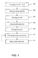
- FIG. 1 is a process flow chart showing the steps of a process that provides a method of ion beam analysis for the high aspect ratio structure analysis of a 3D integrated circuit.
- FIGS. 2-5 show, not to scale, the sample during the process steps, and
- FIG. 7 shows a typical dual beam system that can be used to perform process of FIG. 1 .
- the process of FIG. 1 is described as being performed on a dual beam system in which the electron column is vertical and the ion column is tilted at 52°. In other hardware configurations, the stage tilts will be different to produce the same relative angles between the beam and the work piece.
- step 102 the stage is tilted to an angle of between about 30° and about 33.5°, resulting in an angle of between about 18.5° and about 22° between the ion beam 202 and a normal 204 to the work piece surface 206.
- the angle between ion beam 202 and normal 204 is between 5° and 50°.
- the FIB mills a trench 210 to expose a cross section face 216 as shown in FIG. 2 that includes high aspect ratio holes 212.
- the cross section face 216 is not normal to the sample surface.
- Each arrow shows a scan path of ion beam 202, which scan goes into the plane of the page as the beam scans to mill the trench.
- the trench 210 is preferably sufficiently wide to provide a good secondary electron signal for imaging from ROIs deep in the trench.
- the wide cross sectional area permits the secondary electrons to escape from the bottom of the trench to be detected.
- the cross section of the trench area should be at least twice the size of the region of interest.
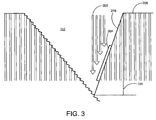
- step 106 the stage is tilted stage to 0° so that an electron beam 302 is oriented normal to the work piece surface 206 and between 18.5° and 22° to the sloped surface 216.
- step 108 a protective layer 304 of platinum, tungsten, or other material is deposited above the region of interest using electron beam-induced deposition as shown in FIG. 3 .
- An electron energy of about 30 keV is preferably used for the best step coverage by increasing the momentum of the electrons to fill in the exposed steps.
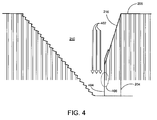
- Step 110 shows the stage is tilted to 52° so that the ion beam is normal to the surface as shown in FIG. 4 .
- Step 112 shows a FIB cross section is performed. A 52° stage tilt makes a perpendicular angle between sample surface and ion column.
- Step 112 forms a vertical cross section of the region of interest that can be imaged or analyzed by a variety of methods, including scanning electron microscopy, x-ray analysis, micro-Raman, or other methods.
- FIG. 4 shows the ion beam 402 makes a vertical cut to expose a vertical surface 404 through the region of interest 406.
- the ion beam 402 processing preferably includes a bulk cut to remove material to form the vertical wall and a cleaning cross section, which removes little material but produces a cleaner surface for observation.
- Work piece surface 206 represents a first surface
- sloped surface 216 represents a second surface
- vertical surface 404 represents a third surface. A portion of the second surface is between the region of interest and the first surface, and the third surface is substantially normal to the first surface.
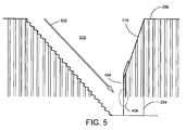
- the electron beam 502 is directed to the sample to form a scanning electron beam image as shown in FIG. 5 .
- steps 112 and 114 are repeated to continue to step through a feature, to form a series of cross-sectional images so that a 3D representation of a feature in the ROI can be formed.
- This process is referred to as "slice-and-view,” which entails repeatedly removing additional material with the ion beam to expose another face of the ROI and then forming an image of the exposed face using the electron beam.
- curtain effects are unavoidable as the perpendicular depth is getting more than a few micrometers deeper.
- curtain effects are removed as materials above ROI are removed and the depth below surface of the ROI is reduced.
- using high energy electrons covers the steps, which enables partially filling any empty hole of high aspect ratio structure with protection materials such as platinum or tungsten. Consequentially, embodiments provide reliable failure analysis or process monitoring.
- Embodiments of the invention shows crisp, clean boundaries between empty channels and the substrate.
- the robust process allows high aspect ratio structure failure analysis without damage to the structure being investigated.
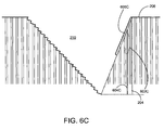
- the high aspect ratio feature can be inspected at different depths from the surface by adjusting the angle of face 216 or the position of the vertical cut through face 216.
- FIGS. 6A, 6B and 6C show regions of interest at different depths below the work piece surface. The samples are shown with the trench 210 milled, but the vertical cut to produce the face for observation is not yet performed.
- the ovals 602A, 602B, and 602C represent regions of interest, and the vertical lines 604A, 604B, and 604C show the position of the vertical ion beam cut through the electron beam deposited protective layer 606A, 606B, and 606C and through the ROI.
- the jagged line shows the ion milling as in step 104 above and FIG. 2 .
- the position of the protective layer 606A, 606B, and 606C varies with the position of the ROI.
- the process for depositing the protective layer preferably fills any holes that are present.
- the ROI is toward the bottom of the channel hole.
- the ROI is about 1 ⁇ 2 way to the bottom of the channel.
- FIG. 6C shows a ROI toward the top of the channel hole.
- the vertical line through the ROI shows the ion beam cut as shown in step 112 through the protective layer. In each case, the distance milled below through the material remaining above the ROI is about the same and is relatively small, so that there is little or no curtaining caused by shading above the ROI.
- FIG. 7 shows a typical dual beam system 710 suitable for practicing the present invention, with a vertically mounted SEM column and a FIB column mounted at an angle of approximately 52° from the vertical.
- Suitable dual beam systems are commercially available, for example, from FEI Company, Hillsboro, Oregon, the assignee of the present application. While an example of suitable hardware is provided below, the invention is not limited to being implemented in any particular type of hardware.
- An electron beam 743 is emitted from a cathode 752 by applying voltage between cathode 752 and an anode 754.
- Electron beam 743 is focused to a fine spot by means of a condensing lens 756 and an objective lens 758.
- Electron beam 743 is scanned two-dimensionally on the specimen by means of a deflection coil 760. Operation of condensing lens 756, objective lens 758, and deflection coil 760 is controlled by power supply and control unit 745.
- Electron beam 743 can be focused onto substrate 722, which is on movable stage 725 within lower chamber 726. When the electrons in the electron beam strike substrate 722, secondary electrons are emitted. These secondary electrons are detected by a secondary electron detector 740 as discussed below.
- Dual beam system 710 also includes focused ion beam (FIB) system 711 which comprises an evacuated chamber having an upper potion 712 within which are located an ion source 714 and a focusing column 716 including extractor electrodes and an electrostatic optical system.
- the axis of focusing column 716 is tilted 52 degrees from the axis of the electron column.
- the upper potion 712 includes an ion source 714, an extraction electrode 715, a focusing element 717, deflection elements 720, and a focused ion beam 718.
- Ion beam 718 passes from ion source 714 through focusing column 716 and between electrostatic deflection means schematically indicated at 720 toward substrate 722, which comprises, for example, a semiconductor device positioned on movable stage 725 within lower chamber 726.
- Stage 725 can preferably move in a horizontal plane (X and Y axes) and vertically (Z axis). Stage 725 can also tilt approximately 60° and rotate about the Z axis.
- a door 761 is opened for inserting substrate 722 onto X-Y stage 725 and also for servicing an internal gas supply reservoir, if one is used. The door is interlocked so that it cannot be opened if the system is under vacuum. Alternatively, an airlock can be used to avoid exposing chamber 726 to atmosphere.
- An ion pump (not shown) is employed for evacuating upper potion 712.
- the chamber 726 is evacuated with turbomolecular and mechanical pumping system 730 under the control of vacuum controller 732.
- the vacuum system provides within chamber 726 a vacuum of between approximately 1.3 x 10 -7 mbar (1 x 10 -7 Torr) and 6.5 x 10 -4 mbar (5 x 10 -4 Torr). If an etch-assisting gas, an etch-retarding gas, or a deposition precursor gas is used, the chamber background pressure may rise, typically to about 1.3 x 10 -5 mbar (1 x 10 -5 Torr).
- the high voltage power supply provides an appropriate acceleration voltage to electrodes in ion beam focusing column focusing 716 for energizing and focusing ion beam 718.
- material is sputtered, that is physically ejected, from the sample.
- ion beam 718 can decompose a precursor gas to deposit a material.
- High voltage power supply 734 is connected to liquid metal ion source 714 as well as to appropriate electrodes in ion beam focusing column 716 for forming an approximately 1 keV to 60 keV ion beam 718 and directing the same toward a sample.
- Deflection controller and amplifier 736 operated in accordance with a prescribed pattern provided by pattern generator 738, is coupled to deflection plates 720 whereby ion beam 718 may be controlled manually or automatically to trace out a corresponding pattern on the upper surface of substrate 722. In some systems the deflection plates are placed before the final lens, as is well known in the art.
- the liquid metal ion source 714 typically provides a metal ion beam of gallium.
- the source typically is capable of being focused into a sub one-tenth micrometer wide beam at substrate 722 for either modifying the substrate 722 by ion milling, enhanced etch, material deposition, or for the purpose of imaging the substrate 722.
- Other ion sources, such as a plasma ion source, can also be used.
- a charged particle detector 740 such as an Everhart-Thornley detector or multichannel plate, used for detecting secondary ion or electron emission is connected to a video circuit 742 that supplies drive signals to video monitor 744 and receives deflection signals from controller 719.
- the location of charged particle detector 740 within lower chamber 726 can vary in different embodiments.
- a charged particle detector 740 can be coaxial with the ion beam and include a hole for allowing the ion beam to pass.
- secondary particles can be collected through a final lens and then diverted off axis for collection.
- a gas delivery system 746 extends into lower chamber 726 for introducing and directing a gaseous vapor toward substrate 722.
- Another gas delivery system is described in U.S. Pat. No. 5,435,850, to Rasmussen for a "Gas Injection System,” also assigned to the assignee of the present invention.
- a metal organic compound can be delivered to the beam impact point to deposit a metal upon impact of the ion beam or the electron beam.
- a precursor gas such as (CH 3 ) 3 Pt(C p CH 3 ) to deposit platinum or tungsten hexacarbonyl to deposit tungsten, can be delivered to be decomposed by the electron beam to provide the protective layer in step 108.
- a system controller 719 controls the operations of the various parts of dual beam system 710. Through system controller 719, a user can cause ion beam 718 or electron beam 743 to be scanned in a desired manner through commands entered into a conventional user interface (not shown). Alternatively, system controller 719 may control dual beam system 710 in accordance with programmed instructions. A preferred controller is in communication with or includes a memory that stores instructions for automatically carrying out the steps of FIG. 1 .
- dual beam system 710 incorporates image recognition software, such as software commercially available from Cognex Corporation, Natick, Massachusetts, to automatically identify regions of interest, and then the system can manually or automatically expose cross sections for imaging in accordance with the invention. For example, the system could automatically locate similar features on semiconductor wafers including multiple devices, and expose and form images of features of interest on different (or the same) devices.
- Particle beam systems suitable for carrying out the present invention are commercially available, for example, from FEI Company, the assignee of the present application.
- the present specification discloses both a method and an apparatus for performing the operations of the method.
- Such apparatus may be specially constructed for the required purposes, or may comprise a general purpose computer or other device selectively activated or reconfigured by a computer program stored in the computer.
- Various general purpose charged particle beam systems may be used with programs in accordance with the teachings herein.
- the construction of more specialized apparatus to perform the required method steps may be appropriate.
- the present specification also implicitly discloses a computer program, in that it would be apparent to the person skilled in the art that the individual steps of the method described herein may be put into effect by computer code.
- the computer program is not intended to be limited to any particular programming language and implementation thereof. It will be appreciated that a variety of programming languages and coding thereof may be used to implement the teachings of the disclosure contained herein.
- the computer program is not intended to be limited to any particular control flow. There are many other variants of the computer program, which can use different control flows without departing from the scope of the invention as claimed.
- Such a computer program may be stored on any computer readable medium.
- the computer readable medium may include storage devices such as magnetic or optical disks, memory chips, or other storage devices suitable for interfacing with a general purpose computer.
- the computer readable medium may also include a hard-wired medium such as exemplified in the Internet system, or wireless medium such as exemplified in the GSM mobile telephone system.
- the computer program when loaded and executed on such a general-purpose computer or controller for a charged particle beam and effectively results in an apparatus that implements the steps of the preferred method.
- the invention may also be implemented as hardware modules. More particular, in the hardware sense, a module is a functional hardware unit designed for use with other components or modules. For example, a module may be implemented using discrete electronic components, or it can form a portion of an entire electronic circuit such as an Application Specific Integrated Circuit (ASIC). Numerous other possibilities exist. Those skilled in the art will appreciate that the system can also be implemented as a combination of hardware and software modules.
- ASIC Application Specific Integrated Circuit
- integrated circuit refers to a set of electronic components and their interconnections (internal electrical circuit elements, collectively) that are patterned on the surface of a microchip.
- semiconductor chip refers generically to an integrated circuit (IC), which may be integral to a semiconductor wafer, separated from a wafer, or packaged for use on a circuit board.
- FIB focused ion beam
- FIB focused ion beam
- the embodiment above describes a 3D NAND- type structures, but the invention is not limited to such structures and is useful, for example, for DRAMS, and for characterizing trenches and other structures, as well as circular holes.
- Some embodiments of the invention provide a method of exposing a region of interest on a work piece using a charged particle beam, comprising: ion beam milling a trench at a first non-normal angle to the work piece top surface to expose a surface adjacent the region of interest and angled with respect to the work piece surface; depositing a protective layer on a portion of the exposed surface adjacent to the region of interest; ion beam milling, at an angle substantially normal to the work piece top surface, a portion of the surface adjacent to the region of interest to expose the region of interest; and observing the region of interest by charged particle beam imaging.
- milling a trench at a first non-normal angle to the work piece top surface includes milling a trench in a region of the work piece having multiple high aspect ratio features.
- the multiple high aspect ratio features are holes.
- depositing a protective layer on a portion of the surface adjacent to the region of interest includes covering steps creating by milling the trench through the high aspect ratio holes.
- Some embodiments further comprise performing multiple subsequent milling steps to sequentially expose different surfaces of the region of interest and viewing each of the different surfaces using charged particle beam imaging.
- milling a trench at a first non-normal angle to the work piece top surface includes milling a trench having a wall at an angle of between 5° and 50° from a normal to the work piece surface.
- milling a trench includes milling a trench having a wall at an angle of about 18° to about 22° from a normal to the work piece surface.
- depositing a protective layer on a portion of the surface adjacent to the region of interest includes using beam-induced deposition.
- using beam-induced deposition comprises electron-beam induced deposition using electrons having energies greater than 10 keV or greater than 20 keV.
- depositing a protective layer on a portion of the surface adjacent to the region of interest comprises depositing using a protective layer using laser-induced deposition or ion beam induced deposition.
- the region of interest includes a portion of a 3D NAND structure or 3D DRAM structures.
- a method of creating a cross section of a portion of a high aspect ratio structure for observation comprising:
- observing the exposed cross section includes scanning electron microscopy, x-ray analysis, micro-Raman, or other methods.
- milling a second cross section through the protective layer parallel to the first cross section to expose a second cross section of the region of interest is a first cross section through the protective layer parallel to the first cross section to expose a second cross section of the region of interest.
- Some embodiments further comprising sequentially milling using the charged particle beam a cross section through the protective layer and observing the exposed cross section using an electron beam to form a series cross sectional images of a feature in the region of interest.
- depositing a protective layer on the wall of the trench comprises depositing a protective layer using beam-induced deposition.
- Some embodiments of the invention provide a method of analyzing a region of interest below a first surface of a work piece, comprising:
- the third surface is substantially orthogonal to the first surface.
- the second surface is tilted with respect to a normal to the first surface at an angle between 5° and 50°.
- the second surface is tilted with respect to a normal to the first surface at an angle between about 18° to about 22°.
- Some embodiments of the invention provide a system for observing a cross section of a sample, comprising:
- the computer memory stores instructions for causing the electron beam to provide electrons having energies greater than 20 keV to deposit the protective layer by electron-beam0-induced deposition.
Landscapes
- Chemical & Material Sciences (AREA)
- Analytical Chemistry (AREA)
- Engineering & Computer Science (AREA)
- Physics & Mathematics (AREA)
- Plasma & Fusion (AREA)
- Mechanical Engineering (AREA)
- Chemical Kinetics & Catalysis (AREA)
- Organic Chemistry (AREA)
- Metallurgy (AREA)
- Materials Engineering (AREA)
- Sampling And Sample Adjustment (AREA)
- Analysing Materials By The Use Of Radiation (AREA)
- Health & Medical Sciences (AREA)
- General Physics & Mathematics (AREA)
- General Health & Medical Sciences (AREA)
- Pathology (AREA)
- Immunology (AREA)
- Biochemistry (AREA)
- Life Sciences & Earth Sciences (AREA)
- Manufacturing & Machinery (AREA)
- Nuclear Medicine, Radiotherapy & Molecular Imaging (AREA)
- Electromagnetism (AREA)
- Power Engineering (AREA)
- Microelectronics & Electronic Packaging (AREA)
- Computer Hardware Design (AREA)
Applications Claiming Priority (2)
| Application Number | Priority Date | Filing Date | Title |
|---|---|---|---|
| US201261710580P | 2012-10-05 | 2012-10-05 | |
| PCT/US2013/063479 WO2014055876A1 (en) | 2012-10-05 | 2013-10-04 | High aspect ratio structure analysis |
Publications (3)
| Publication Number | Publication Date |
|---|---|
| EP2904382A1 EP2904382A1 (en) | 2015-08-12 |
| EP2904382A4 EP2904382A4 (en) | 2015-08-19 |
| EP2904382B1 true EP2904382B1 (en) | 2016-08-24 |
Family
ID=50435471
Family Applications (1)
| Application Number | Title | Priority Date | Filing Date |
|---|---|---|---|
| EP13844339.5A Not-in-force EP2904382B1 (en) | 2012-10-05 | 2013-10-04 | High aspect ratio structure analysis |
Country Status (7)
| Country | Link |
|---|---|
| US (1) | US9741536B2 (zh) |
| EP (1) | EP2904382B1 (zh) |
| JP (1) | JP6199978B2 (zh) |
| KR (1) | KR102155834B1 (zh) |
| CN (1) | CN104685348B (zh) |
| TW (1) | TWI628702B (zh) |
| WO (1) | WO2014055876A1 (zh) |
Families Citing this family (13)
| Publication number | Priority date | Publication date | Assignee | Title |
|---|---|---|---|---|
| WO2014055982A1 (en) * | 2012-10-05 | 2014-04-10 | Fei Company | Bulk deposition for tilted mill protection |
| CN104685617B (zh) | 2012-10-05 | 2018-11-30 | Fei 公司 | 用于减少带电粒子束样品制备中的幕化的方法和系统 |
| CN104813459B (zh) | 2012-10-05 | 2018-01-19 | Fei 公司 | 多维结构访问 |
| TWI628702B (zh) | 2012-10-05 | 2018-07-01 | Fei公司 | 高「高寬比」結構之分析 |
| CN104885196B (zh) | 2012-12-31 | 2018-02-06 | Fei 公司 | 带电粒子束系统以及使用带电粒子束诱发沉积来填充孔的方法 |
| CZ2013547A3 (cs) | 2013-07-11 | 2014-11-19 | Tescan Orsay Holding, A.S. | Způsob opracovávání vzorku v zařízení se dvěma nebo více částicovými svazky a zařízení k jeho provádění |
| US9564291B1 (en) * | 2014-01-27 | 2017-02-07 | Mochii, Inc. | Hybrid charged-particle beam and light beam microscopy |
| KR102537699B1 (ko) | 2017-12-26 | 2023-05-26 | 삼성전자주식회사 | 반도체 장치의 검사 방법 |
| US11177110B2 (en) * | 2018-02-06 | 2021-11-16 | Howard Hughes Medical Institute | Volume scanning electron microscopy of serial thick tissue sections with gas cluster milling |
| US10811219B2 (en) * | 2018-08-07 | 2020-10-20 | Applied Materials Israel Ltd. | Method for evaluating a region of an object |
| US10903044B1 (en) * | 2020-02-12 | 2021-01-26 | Applied Materials Israel Ltd. | Filling empty structures with deposition under high-energy SEM for uniform DE layering |
| KR20210132836A (ko) | 2020-04-28 | 2021-11-05 | 삼성전자주식회사 | 하전입자를 이용한 반도체 소자 검사장치 및 이를 이용한 반도체 소자의 검사방법 |
| TWI826123B (zh) * | 2021-12-21 | 2023-12-11 | 德商卡爾蔡司Smt有限公司 | 以更高的精度對半導體晶圓進行3d體積檢測的方法和檢測系統 |
Family Cites Families (36)
| Publication number | Priority date | Publication date | Assignee | Title |
|---|---|---|---|---|
| US4460634A (en) * | 1979-12-29 | 1984-07-17 | Masaaki Hasegawa | Adhesive sheet and method for manufacturing the same |
| US4460434A (en) * | 1982-04-15 | 1984-07-17 | At&T Bell Laboratories | Method for planarizing patterned surfaces |
| US5435850A (en) | 1993-09-17 | 1995-07-25 | Fei Company | Gas injection system |
| US5851413A (en) | 1996-06-19 | 1998-12-22 | Micrion Corporation | Gas delivery systems for particle beam processing |
| US6127277A (en) * | 1996-07-03 | 2000-10-03 | Tegal Corporation | Method and apparatus for etching a semiconductor wafer with features having vertical sidewalls |
| US20010003035A1 (en) * | 1998-09-10 | 2001-06-07 | Robert G. Ozarski | Diffraction grating and fabrication technique for same |
| JP3805547B2 (ja) * | 1999-01-21 | 2006-08-02 | 株式会社日立製作所 | 試料作製装置 |
| JP2001264225A (ja) * | 2000-03-15 | 2001-09-26 | Hitachi Ltd | 試料作製方法 |
| US6517734B1 (en) * | 2000-07-13 | 2003-02-11 | Network Photonics, Inc. | Grating fabrication process using combined crystalline-dependent and crystalline-independent etching |
| EP1209737B2 (en) | 2000-11-06 | 2014-04-30 | Hitachi, Ltd. | Method for specimen fabrication |
| US7108819B2 (en) * | 2001-08-27 | 2006-09-19 | The Boeing Company | Process for fabricating high aspect ratio embossing tool and microstructures |
| US20070087572A1 (en) | 2004-02-27 | 2007-04-19 | Erwan Le Roy | Method and apparatus for the improvement of material/voltage contrast |
| JP5033314B2 (ja) * | 2004-09-29 | 2012-09-26 | 株式会社日立ハイテクノロジーズ | イオンビーム加工装置及び加工方法 |
| JP4927345B2 (ja) | 2005-04-07 | 2012-05-09 | ルネサスエレクトロニクス株式会社 | 試料体の加工観察装置及び試料体の観察方法 |
| CN100449722C (zh) | 2005-12-08 | 2009-01-07 | 中芯国际集成电路制造(上海)有限公司 | 一种测定深沟槽失效深度的方法 |
| JP5101845B2 (ja) * | 2006-08-21 | 2012-12-19 | エスアイアイ・ナノテクノロジー株式会社 | 集束イオンビーム装置ならびにそれを用いた試料断面作製方法および薄片試料作製方法 |
| CN101153855A (zh) | 2006-09-30 | 2008-04-02 | 中芯国际集成电路制造(上海)有限公司 | 试样台 |
| US8303833B2 (en) * | 2007-06-21 | 2012-11-06 | Fei Company | High resolution plasma etch |
| JP5873227B2 (ja) | 2007-12-06 | 2016-03-01 | エフ・イ−・アイ・カンパニー | デコレーションを用いたスライス・アンド・ビュー |
| US8595860B2 (en) * | 2007-12-28 | 2013-11-26 | Bruker Nano, Inc. | Method of fabricating a probe device for a metrology instrument and a probe device produced thereby |
| WO2009114291A2 (en) * | 2008-03-14 | 2009-09-17 | Research Triangle Institute | Faraday cup array integrated with a readout ic and method for manufacture thereof |
| JP5175008B2 (ja) * | 2009-02-20 | 2013-04-03 | 株式会社日立ハイテクサイエンス | ミクロ断面加工方法 |
| JP5378185B2 (ja) | 2009-12-08 | 2013-12-25 | 株式会社日立ハイテクノロジーズ | 集束イオンビーム装置、及び集束イオンビーム加工方法 |
| DE102011002583B9 (de) * | 2011-01-12 | 2018-06-28 | Carl Zeiss Microscopy Gmbh | Teilchenstrahlgerät und Verfahren zur Bearbeitung und/oder Analyse einer Probe |
| CN103403520B (zh) | 2011-01-28 | 2015-12-23 | Fei公司 | Tem样品制备 |
| JP5825797B2 (ja) * | 2011-02-08 | 2015-12-02 | 株式会社ブリヂストン | 高分子材料の評価方法 |
| US8859963B2 (en) | 2011-06-03 | 2014-10-14 | Fei Company | Methods for preparing thin samples for TEM imaging |
| US8822921B2 (en) | 2011-06-03 | 2014-09-02 | Fei Company | Method for preparing samples for imaging |
| EP2749863A3 (en) | 2012-12-31 | 2016-05-04 | Fei Company | Method for preparing samples for imaging |
| US8912490B2 (en) | 2011-06-03 | 2014-12-16 | Fei Company | Method for preparing samples for imaging |
| JP6174584B2 (ja) | 2011-09-12 | 2017-08-02 | エフ・イ−・アイ・カンパニー | 視射角ミル |
| EP2786113B1 (en) | 2011-12-01 | 2017-03-01 | FEI Company | High throughput tem preparation process for backside thinning of cross-sectional view lamella |
| US9733164B2 (en) | 2012-06-11 | 2017-08-15 | Fei Company | Lamella creation method and device using fixed-angle beam and rotating sample stage |
| TWI628702B (zh) | 2012-10-05 | 2018-07-01 | Fei公司 | 高「高寬比」結構之分析 |
| WO2014055982A1 (en) | 2012-10-05 | 2014-04-10 | Fei Company | Bulk deposition for tilted mill protection |
| CN104885196B (zh) | 2012-12-31 | 2018-02-06 | Fei 公司 | 带电粒子束系统以及使用带电粒子束诱发沉积来填充孔的方法 |
-
2013
- 2013-10-04 TW TW102136150A patent/TWI628702B/zh active
- 2013-10-04 JP JP2015535822A patent/JP6199978B2/ja active Active
- 2013-10-04 US US14/433,354 patent/US9741536B2/en active Active
- 2013-10-04 EP EP13844339.5A patent/EP2904382B1/en not_active Not-in-force
- 2013-10-04 KR KR1020157008578A patent/KR102155834B1/ko active IP Right Grant
- 2013-10-04 CN CN201380052272.XA patent/CN104685348B/zh active Active
- 2013-10-04 WO PCT/US2013/063479 patent/WO2014055876A1/en active Application Filing
Also Published As
| Publication number | Publication date |
|---|---|
| WO2014055876A4 (en) | 2014-05-30 |
| JP2015533215A (ja) | 2015-11-19 |
| TW201421546A (zh) | 2014-06-01 |
| KR102155834B1 (ko) | 2020-09-14 |
| EP2904382A4 (en) | 2015-08-19 |
| US20150243478A1 (en) | 2015-08-27 |
| CN104685348A (zh) | 2015-06-03 |
| EP2904382A1 (en) | 2015-08-12 |
| TWI628702B (zh) | 2018-07-01 |
| JP6199978B2 (ja) | 2017-09-20 |
| US9741536B2 (en) | 2017-08-22 |
| WO2014055876A1 (en) | 2014-04-10 |
| CN104685348B (zh) | 2017-12-12 |
| KR20150060748A (ko) | 2015-06-03 |
Similar Documents
| Publication | Publication Date | Title |
|---|---|---|
| EP2904382B1 (en) | High aspect ratio structure analysis | |
| EP2903773B1 (en) | Bulk deposition for tilted mill protection | |
| US8399831B2 (en) | Forming an image while milling a work piece | |
| EP2904633B1 (en) | Multidimensional structural access | |
| JP6644127B2 (ja) | 荷電粒子ビーム試料作製におけるカーテニングを低減させる方法およびシステム | |
| EP2756282A1 (en) | Glancing angle mill | |
| US9384982B2 (en) | Depositing material into high aspect ratio structures | |
| JP6192695B2 (ja) | 自動スライス・アンド・ビュー下部切削 |
Legal Events
| Date | Code | Title | Description |
|---|---|---|---|
| PUAI | Public reference made under article 153(3) epc to a published international application that has entered the european phase |
Free format text: ORIGINAL CODE: 0009012 |
|
| 17P | Request for examination filed |
Effective date: 20150402 |
|
| AK | Designated contracting states |
Kind code of ref document: A1 Designated state(s): AL AT BE BG CH CY CZ DE DK EE ES FI FR GB GR HR HU IE IS IT LI LT LU LV MC MK MT NL NO PL PT RO RS SE SI SK SM TR |
|
| AX | Request for extension of the european patent |
Extension state: BA ME |
|
| RA4 | Supplementary search report drawn up and despatched (corrected) |
Effective date: 20150721 |
|
| RIC1 | Information provided on ipc code assigned before grant |
Ipc: G01N 23/00 20060101AFI20150715BHEP Ipc: H01J 37/317 20060101ALI20150715BHEP Ipc: H01J 37/305 20060101ALI20150715BHEP Ipc: G01B 15/00 20060101ALI20150715BHEP Ipc: B23K 15/08 20060101ALI20150715BHEP Ipc: G01N 1/32 20060101ALI20150715BHEP |
|
| RIN1 | Information on inventor provided before grant (corrected) |
Inventor name: STONE, STACEY Inventor name: SCHMIDT, MICHAEL Inventor name: LEE, SANG HOON Inventor name: BLACKWOOD, JEFFREY |
|
| DAX | Request for extension of the european patent (deleted) | ||
| GRAP | Despatch of communication of intention to grant a patent |
Free format text: ORIGINAL CODE: EPIDOSNIGR1 |
|
| INTG | Intention to grant announced |
Effective date: 20160404 |
|
| GRAS | Grant fee paid |
Free format text: ORIGINAL CODE: EPIDOSNIGR3 |
|
| GRAA | (expected) grant |
Free format text: ORIGINAL CODE: 0009210 |
|
| AK | Designated contracting states |
Kind code of ref document: B1 Designated state(s): AL AT BE BG CH CY CZ DE DK EE ES FI FR GB GR HR HU IE IS IT LI LT LU LV MC MK MT NL NO PL PT RO RS SE SI SK SM TR |
|
| REG | Reference to a national code |
Ref country code: GB Ref legal event code: FG4D |
|
| REG | Reference to a national code |
Ref country code: CH Ref legal event code: EP |
|
| REG | Reference to a national code |
Ref country code: AT Ref legal event code: REF Ref document number: 823538 Country of ref document: AT Kind code of ref document: T Effective date: 20160915 |
|
| REG | Reference to a national code |
Ref country code: IE Ref legal event code: FG4D |
|
| REG | Reference to a national code |
Ref country code: DE Ref legal event code: R096 Ref document number: 602013010797 Country of ref document: DE |
|
| REG | Reference to a national code |
Ref country code: LT Ref legal event code: MG4D |
|
| REG | Reference to a national code |
Ref country code: NL Ref legal event code: MP Effective date: 20160824 |
|
| REG | Reference to a national code |
Ref country code: AT Ref legal event code: MK05 Ref document number: 823538 Country of ref document: AT Kind code of ref document: T Effective date: 20160824 |
|
| PG25 | Lapsed in a contracting state [announced via postgrant information from national office to epo] |
Ref country code: NL Free format text: LAPSE BECAUSE OF FAILURE TO SUBMIT A TRANSLATION OF THE DESCRIPTION OR TO PAY THE FEE WITHIN THE PRESCRIBED TIME-LIMIT Effective date: 20160824 Ref country code: RS Free format text: LAPSE BECAUSE OF FAILURE TO SUBMIT A TRANSLATION OF THE DESCRIPTION OR TO PAY THE FEE WITHIN THE PRESCRIBED TIME-LIMIT Effective date: 20160824 Ref country code: NO Free format text: LAPSE BECAUSE OF FAILURE TO SUBMIT A TRANSLATION OF THE DESCRIPTION OR TO PAY THE FEE WITHIN THE PRESCRIBED TIME-LIMIT Effective date: 20161124 Ref country code: IT Free format text: LAPSE BECAUSE OF FAILURE TO SUBMIT A TRANSLATION OF THE DESCRIPTION OR TO PAY THE FEE WITHIN THE PRESCRIBED TIME-LIMIT Effective date: 20160824 Ref country code: LT Free format text: LAPSE BECAUSE OF FAILURE TO SUBMIT A TRANSLATION OF THE DESCRIPTION OR TO PAY THE FEE WITHIN THE PRESCRIBED TIME-LIMIT Effective date: 20160824 Ref country code: FI Free format text: LAPSE BECAUSE OF FAILURE TO SUBMIT A TRANSLATION OF THE DESCRIPTION OR TO PAY THE FEE WITHIN THE PRESCRIBED TIME-LIMIT Effective date: 20160824 Ref country code: HR Free format text: LAPSE BECAUSE OF FAILURE TO SUBMIT A TRANSLATION OF THE DESCRIPTION OR TO PAY THE FEE WITHIN THE PRESCRIBED TIME-LIMIT Effective date: 20160824 |
|
| PG25 | Lapsed in a contracting state [announced via postgrant information from national office to epo] |
Ref country code: GR Free format text: LAPSE BECAUSE OF FAILURE TO SUBMIT A TRANSLATION OF THE DESCRIPTION OR TO PAY THE FEE WITHIN THE PRESCRIBED TIME-LIMIT Effective date: 20161125 Ref country code: AT Free format text: LAPSE BECAUSE OF FAILURE TO SUBMIT A TRANSLATION OF THE DESCRIPTION OR TO PAY THE FEE WITHIN THE PRESCRIBED TIME-LIMIT Effective date: 20160824 Ref country code: BE Free format text: LAPSE BECAUSE OF NON-PAYMENT OF DUE FEES Effective date: 20161031 Ref country code: ES Free format text: LAPSE BECAUSE OF FAILURE TO SUBMIT A TRANSLATION OF THE DESCRIPTION OR TO PAY THE FEE WITHIN THE PRESCRIBED TIME-LIMIT Effective date: 20160824 Ref country code: SE Free format text: LAPSE BECAUSE OF FAILURE TO SUBMIT A TRANSLATION OF THE DESCRIPTION OR TO PAY THE FEE WITHIN THE PRESCRIBED TIME-LIMIT Effective date: 20160824 Ref country code: PT Free format text: LAPSE BECAUSE OF FAILURE TO SUBMIT A TRANSLATION OF THE DESCRIPTION OR TO PAY THE FEE WITHIN THE PRESCRIBED TIME-LIMIT Effective date: 20161226 Ref country code: LV Free format text: LAPSE BECAUSE OF FAILURE TO SUBMIT A TRANSLATION OF THE DESCRIPTION OR TO PAY THE FEE WITHIN THE PRESCRIBED TIME-LIMIT Effective date: 20160824 |
|
| PG25 | Lapsed in a contracting state [announced via postgrant information from national office to epo] |
Ref country code: EE Free format text: LAPSE BECAUSE OF FAILURE TO SUBMIT A TRANSLATION OF THE DESCRIPTION OR TO PAY THE FEE WITHIN THE PRESCRIBED TIME-LIMIT Effective date: 20160824 Ref country code: RO Free format text: LAPSE BECAUSE OF FAILURE TO SUBMIT A TRANSLATION OF THE DESCRIPTION OR TO PAY THE FEE WITHIN THE PRESCRIBED TIME-LIMIT Effective date: 20160824 |
|
| REG | Reference to a national code |
Ref country code: DE Ref legal event code: R119 Ref document number: 602013010797 Country of ref document: DE |
|
| PG25 | Lapsed in a contracting state [announced via postgrant information from national office to epo] |
Ref country code: PL Free format text: LAPSE BECAUSE OF FAILURE TO SUBMIT A TRANSLATION OF THE DESCRIPTION OR TO PAY THE FEE WITHIN THE PRESCRIBED TIME-LIMIT Effective date: 20160824 Ref country code: SM Free format text: LAPSE BECAUSE OF FAILURE TO SUBMIT A TRANSLATION OF THE DESCRIPTION OR TO PAY THE FEE WITHIN THE PRESCRIBED TIME-LIMIT Effective date: 20160824 Ref country code: DK Free format text: LAPSE BECAUSE OF FAILURE TO SUBMIT A TRANSLATION OF THE DESCRIPTION OR TO PAY THE FEE WITHIN THE PRESCRIBED TIME-LIMIT Effective date: 20160824 Ref country code: BG Free format text: LAPSE BECAUSE OF FAILURE TO SUBMIT A TRANSLATION OF THE DESCRIPTION OR TO PAY THE FEE WITHIN THE PRESCRIBED TIME-LIMIT Effective date: 20161124 Ref country code: CZ Free format text: LAPSE BECAUSE OF FAILURE TO SUBMIT A TRANSLATION OF THE DESCRIPTION OR TO PAY THE FEE WITHIN THE PRESCRIBED TIME-LIMIT Effective date: 20160824 Ref country code: BE Free format text: LAPSE BECAUSE OF FAILURE TO SUBMIT A TRANSLATION OF THE DESCRIPTION OR TO PAY THE FEE WITHIN THE PRESCRIBED TIME-LIMIT Effective date: 20160824 Ref country code: SK Free format text: LAPSE BECAUSE OF FAILURE TO SUBMIT A TRANSLATION OF THE DESCRIPTION OR TO PAY THE FEE WITHIN THE PRESCRIBED TIME-LIMIT Effective date: 20160824 |
|
| REG | Reference to a national code |
Ref country code: CH Ref legal event code: PL |
|
| PLBE | No opposition filed within time limit |
Free format text: ORIGINAL CODE: 0009261 |
|
| STAA | Information on the status of an ep patent application or granted ep patent |
Free format text: STATUS: NO OPPOSITION FILED WITHIN TIME LIMIT |
|
| REG | Reference to a national code |
Ref country code: IE Ref legal event code: MM4A |
|
| REG | Reference to a national code |
Ref country code: FR Ref legal event code: ST Effective date: 20170630 |
|
| PG25 | Lapsed in a contracting state [announced via postgrant information from national office to epo] |
Ref country code: FR Free format text: LAPSE BECAUSE OF NON-PAYMENT OF DUE FEES Effective date: 20161102 Ref country code: CH Free format text: LAPSE BECAUSE OF NON-PAYMENT OF DUE FEES Effective date: 20161031 Ref country code: LI Free format text: LAPSE BECAUSE OF NON-PAYMENT OF DUE FEES Effective date: 20161031 Ref country code: DE Free format text: LAPSE BECAUSE OF NON-PAYMENT OF DUE FEES Effective date: 20170503 |
|
| 26N | No opposition filed |
Effective date: 20170526 |
|
| PG25 | Lapsed in a contracting state [announced via postgrant information from national office to epo] |
Ref country code: SI Free format text: LAPSE BECAUSE OF FAILURE TO SUBMIT A TRANSLATION OF THE DESCRIPTION OR TO PAY THE FEE WITHIN THE PRESCRIBED TIME-LIMIT Effective date: 20160824 Ref country code: LU Free format text: LAPSE BECAUSE OF NON-PAYMENT OF DUE FEES Effective date: 20161004 |
|
| PG25 | Lapsed in a contracting state [announced via postgrant information from national office to epo] |
Ref country code: IE Free format text: LAPSE BECAUSE OF NON-PAYMENT OF DUE FEES Effective date: 20161004 |
|
| PG25 | Lapsed in a contracting state [announced via postgrant information from national office to epo] |
Ref country code: HU Free format text: LAPSE BECAUSE OF FAILURE TO SUBMIT A TRANSLATION OF THE DESCRIPTION OR TO PAY THE FEE WITHIN THE PRESCRIBED TIME-LIMIT; INVALID AB INITIO Effective date: 20131004 |
|
| GBPC | Gb: european patent ceased through non-payment of renewal fee |
Effective date: 20171004 |
|
| PG25 | Lapsed in a contracting state [announced via postgrant information from national office to epo] |
Ref country code: CY Free format text: LAPSE BECAUSE OF FAILURE TO SUBMIT A TRANSLATION OF THE DESCRIPTION OR TO PAY THE FEE WITHIN THE PRESCRIBED TIME-LIMIT Effective date: 20160824 Ref country code: MT Free format text: LAPSE BECAUSE OF NON-PAYMENT OF DUE FEES Effective date: 20161031 Ref country code: IS Free format text: LAPSE BECAUSE OF FAILURE TO SUBMIT A TRANSLATION OF THE DESCRIPTION OR TO PAY THE FEE WITHIN THE PRESCRIBED TIME-LIMIT Effective date: 20160824 Ref country code: MK Free format text: LAPSE BECAUSE OF FAILURE TO SUBMIT A TRANSLATION OF THE DESCRIPTION OR TO PAY THE FEE WITHIN THE PRESCRIBED TIME-LIMIT Effective date: 20160824 Ref country code: MC Free format text: LAPSE BECAUSE OF FAILURE TO SUBMIT A TRANSLATION OF THE DESCRIPTION OR TO PAY THE FEE WITHIN THE PRESCRIBED TIME-LIMIT Effective date: 20160824 |
|
| PG25 | Lapsed in a contracting state [announced via postgrant information from national office to epo] |
Ref country code: GB Free format text: LAPSE BECAUSE OF NON-PAYMENT OF DUE FEES Effective date: 20171004 |
|
| PG25 | Lapsed in a contracting state [announced via postgrant information from national office to epo] |
Ref country code: TR Free format text: LAPSE BECAUSE OF FAILURE TO SUBMIT A TRANSLATION OF THE DESCRIPTION OR TO PAY THE FEE WITHIN THE PRESCRIBED TIME-LIMIT Effective date: 20160824 Ref country code: AL Free format text: LAPSE BECAUSE OF FAILURE TO SUBMIT A TRANSLATION OF THE DESCRIPTION OR TO PAY THE FEE WITHIN THE PRESCRIBED TIME-LIMIT Effective date: 20160824 |