EP2899755A1 - Semiconductor package - Google Patents
Semiconductor package Download PDFInfo
- Publication number
- EP2899755A1 EP2899755A1 EP15151288.6A EP15151288A EP2899755A1 EP 2899755 A1 EP2899755 A1 EP 2899755A1 EP 15151288 A EP15151288 A EP 15151288A EP 2899755 A1 EP2899755 A1 EP 2899755A1
- Authority
- EP
- European Patent Office
- Prior art keywords
- semiconductor die
- pads
- semiconductor
- package
- vias
- Prior art date
- Legal status (The legal status is an assumption and is not a legal conclusion. Google has not performed a legal analysis and makes no representation as to the accuracy of the status listed.)
- Withdrawn
Links
Images

Classifications
-
- H—ELECTRICITY
- H10—SEMICONDUCTOR DEVICES; ELECTRIC SOLID-STATE DEVICES NOT OTHERWISE PROVIDED FOR
- H10W—GENERIC PACKAGES, INTERCONNECTIONS, CONNECTORS OR OTHER CONSTRUCTIONAL DETAILS OF DEVICES COVERED BY CLASS H10
- H10W90/00—Package configurations
-
- H—ELECTRICITY
- H10—SEMICONDUCTOR DEVICES; ELECTRIC SOLID-STATE DEVICES NOT OTHERWISE PROVIDED FOR
- H10W—GENERIC PACKAGES, INTERCONNECTIONS, CONNECTORS OR OTHER CONSTRUCTIONAL DETAILS OF DEVICES COVERED BY CLASS H10
- H10W20/00—Interconnections in chips, wafers or substrates
- H10W20/20—Interconnections within wafers or substrates, e.g. through-silicon vias [TSV]
-
- H—ELECTRICITY
- H10—SEMICONDUCTOR DEVICES; ELECTRIC SOLID-STATE DEVICES NOT OTHERWISE PROVIDED FOR
- H10W—GENERIC PACKAGES, INTERCONNECTIONS, CONNECTORS OR OTHER CONSTRUCTIONAL DETAILS OF DEVICES COVERED BY CLASS H10
- H10W20/00—Interconnections in chips, wafers or substrates
- H10W20/40—Interconnections external to wafers or substrates, e.g. back-end-of-line [BEOL] metallisations or vias connecting to gate electrodes
- H10W20/41—Interconnections external to wafers or substrates, e.g. back-end-of-line [BEOL] metallisations or vias connecting to gate electrodes characterised by their conductive parts
- H10W20/427—Power or ground buses
-
- H—ELECTRICITY
- H10—SEMICONDUCTOR DEVICES; ELECTRIC SOLID-STATE DEVICES NOT OTHERWISE PROVIDED FOR
- H10W—GENERIC PACKAGES, INTERCONNECTIONS, CONNECTORS OR OTHER CONSTRUCTIONAL DETAILS OF DEVICES COVERED BY CLASS H10
- H10W72/00—Interconnections or connectors in packages
- H10W72/20—Bump connectors, e.g. solder bumps or copper pillars; Dummy bumps; Thermal bumps
-
- H—ELECTRICITY
- H10—SEMICONDUCTOR DEVICES; ELECTRIC SOLID-STATE DEVICES NOT OTHERWISE PROVIDED FOR
- H10W—GENERIC PACKAGES, INTERCONNECTIONS, CONNECTORS OR OTHER CONSTRUCTIONAL DETAILS OF DEVICES COVERED BY CLASS H10
- H10W74/00—Encapsulations, e.g. protective coatings
- H10W74/10—Encapsulations, e.g. protective coatings characterised by their shape or disposition
- H10W74/111—Encapsulations, e.g. protective coatings characterised by their shape or disposition the semiconductor body being completely enclosed
- H10W74/114—Encapsulations, e.g. protective coatings characterised by their shape or disposition the semiconductor body being completely enclosed by a substrate and the encapsulations
- H10W74/117—Encapsulations, e.g. protective coatings characterised by their shape or disposition the semiconductor body being completely enclosed by a substrate and the encapsulations the substrate having spherical bumps for external connection
-
- H—ELECTRICITY
- H10—SEMICONDUCTOR DEVICES; ELECTRIC SOLID-STATE DEVICES NOT OTHERWISE PROVIDED FOR
- H10W—GENERIC PACKAGES, INTERCONNECTIONS, CONNECTORS OR OTHER CONSTRUCTIONAL DETAILS OF DEVICES COVERED BY CLASS H10
- H10W72/00—Interconnections or connectors in packages
- H10W72/20—Bump connectors, e.g. solder bumps or copper pillars; Dummy bumps; Thermal bumps
- H10W72/241—Dispositions, e.g. layouts
- H10W72/244—Dispositions, e.g. layouts relative to underlying supporting features, e.g. bond pads, RDLs or vias
-
- H—ELECTRICITY
- H10—SEMICONDUCTOR DEVICES; ELECTRIC SOLID-STATE DEVICES NOT OTHERWISE PROVIDED FOR
- H10W—GENERIC PACKAGES, INTERCONNECTIONS, CONNECTORS OR OTHER CONSTRUCTIONAL DETAILS OF DEVICES COVERED BY CLASS H10
- H10W74/00—Encapsulations, e.g. protective coatings
-
- H—ELECTRICITY
- H10—SEMICONDUCTOR DEVICES; ELECTRIC SOLID-STATE DEVICES NOT OTHERWISE PROVIDED FOR
- H10W—GENERIC PACKAGES, INTERCONNECTIONS, CONNECTORS OR OTHER CONSTRUCTIONAL DETAILS OF DEVICES COVERED BY CLASS H10
- H10W90/00—Package configurations
- H10W90/20—Configurations of stacked chips
- H10W90/297—Configurations of stacked chips characterised by the through-semiconductor vias [TSVs] in the stacked chips
-
- H—ELECTRICITY
- H10—SEMICONDUCTOR DEVICES; ELECTRIC SOLID-STATE DEVICES NOT OTHERWISE PROVIDED FOR
- H10W—GENERIC PACKAGES, INTERCONNECTIONS, CONNECTORS OR OTHER CONSTRUCTIONAL DETAILS OF DEVICES COVERED BY CLASS H10
- H10W90/00—Package configurations
- H10W90/701—Package configurations characterised by the relative positions of pads or connectors relative to package parts
- H10W90/721—Package configurations characterised by the relative positions of pads or connectors relative to package parts of bump connectors
- H10W90/722—Package configurations characterised by the relative positions of pads or connectors relative to package parts of bump connectors between stacked chips
-
- H—ELECTRICITY
- H10—SEMICONDUCTOR DEVICES; ELECTRIC SOLID-STATE DEVICES NOT OTHERWISE PROVIDED FOR
- H10W—GENERIC PACKAGES, INTERCONNECTIONS, CONNECTORS OR OTHER CONSTRUCTIONAL DETAILS OF DEVICES COVERED BY CLASS H10
- H10W90/00—Package configurations
- H10W90/701—Package configurations characterised by the relative positions of pads or connectors relative to package parts
- H10W90/721—Package configurations characterised by the relative positions of pads or connectors relative to package parts of bump connectors
- H10W90/724—Package configurations characterised by the relative positions of pads or connectors relative to package parts of bump connectors between a chip and a stacked insulating package substrate, interposer or RDL
Definitions
- the present invention relates to a semiconductor package, and in particular relates to a via design for a semiconductor package.
- I/O connections For a semiconductor chip package design, an increased amount of input/output (I/O) connections for multi-functional chips is required. The impact of this will be pressure on printed circuit board (PCB) fabricators to minimize linewidth and space or to develop direct chip attach (DCA) semiconductors.
- PCB printed circuit board
- DCA direct chip attach
- the increased amount of input/output connections of a multi-functional chip package may induce thermal electrical problems, for example, problems with heat dissipation, cross talk, signal propagation delay, electromagnetic interference in RF circuits, etc. The thermal electrical problems may affect the reliability and quality of products.
- a semiconductor package is provided.
- An exemplary embodiment of a semiconductor package includes a first semiconductor die having pads thereon.
- a first via and a second via are respectively disposed on the first semiconductor die.
- the first via connects to at least two of the pads of the first semiconductor die.
- Another exemplary embodiment of a semiconductor package includes a first semiconductor die having a first pad and a second pad thereon.
- the first and second pads are both power pads or ground pads.
- a first via is disposed on the first semiconductor die, wherein the first via connects to both the first and second pads of the first semiconductor die.
- Yet another exemplary embodiment of a semiconductor package includes a first semiconductor die having pads thereon.
- a first via is disposed on the first semiconductor die.
- the first conductive bump connects to the pads of the first semiconductor die.
- the first via is mesh-shaped or ring-shaped from a plan view.
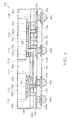
- FIG. 1 is a cross-sectional view of a semiconductor package 500 in accordance with some embodiments of the disclosure.
- the semiconductor package 500 can be a wafer level package assembly using vias connecting a semiconductor device to a redistribution layer (RDL) structure.
- the semiconductor package 500 includes a redistribution layer (RDL) structure 300, a first semiconductor die 310, a second semiconductor die 312 and vias 218a-218c in accordance with some embodiments of the disclosure.
- RDL redistribution layer
- the first semiconductor die 310 and the second semiconductor die 312 shown in FIG. 1 are only an example and are not a limitation on the number of semiconductor dies in the semiconductor package of the present invention.
- the semiconductor package 500 includes a single semiconductor die or more than two semiconductor dies. Also, for the clear illustration of the vias used for power or ground pads of the semiconductor dies, the vias used as electrical connections for a signal pad of a signal semiconductor die are not shown in the figures ( FIGS. 1 and 2 ).
- the first semiconductor die 310 and the second semiconductor die 312 separated from each other are attached to a carrier (not shown) through an adhesive layer (not shown).
- a backside surface 310a of the first semiconductor die 310 and a backside surface 312a of the second semiconductor die 312 are in contact with the carrier.
- a top surface 310b of the first semiconductor die 310 and a top surface 312b of the second semiconductor die 312 may face away from the carrier 112.
- the carrier may be configured to provide structural rigidity or a base for deposition of subsequent non-rigid layers.
- the second semiconductor die 312 is disposed beside the first semiconductor die 310. In some other embodiments, the second semiconductor die 312 is disposed on the first semiconductor die 310. Circuitries of the first semiconductor die 310 and the second semiconductor die 312 are disposed close to the top surfaces 310b and 312b, respectively. In some embodiments, pads 202a-202d and 202g are disposed on the top surface 310b of the first semiconductor die 310 to be electrically connected to the circuitry of the first semiconductor die 310. Pads 202e, 202f and 202h are disposed on the top surface 312b of the second semiconductor die 312 to be electrically connected to the circuitry of the second semiconductor die 312.
- the pads 202a-202d and 202g belong to the uppermost metal layer of the interconnection structure (not shown) of the first semiconductor die 310.
- the pads 202e, 202f and 202h belong to the uppermost metal layer of the interconnection structure (not shown) of the second semiconductor die 312.
- the pads 202a-202d and 202g are arranged in the central area of the first semiconductor die 310 to be used to transmit ground or power signals of the first semiconductor die 310.
- the pads 202e, 202f and 202h are arranged in the central area of the second semiconductor die 312 to be used to transmit ground or power signals of the second semiconductor die 312. Therefore, the pads 202a-202h may serve as ground or power pads.
- a molding compound 308a may be applied to the carrier, and may surround the first semiconductor die 310 and the second semiconductor die 312, and filling any gaps around the first semiconductor die 310 and the second semiconductor die 312 to form a molded substrate 308.
- the molded substrate 308 also cover the top surfaces 310b and 312b of the first semiconductor die 310 and the second semiconductor die 312.
- the molded substrate 308 may be formed of a nonconductive material, such as an epoxy, a resin, a moldable polymer, or the like.
- the molding compound 308a may be applied while substantially liquid, and then may be cured through a chemical reaction, such as in an epoxy or resin.
- the molding compound 308a may be an ultraviolet (UV) or thermally cured polymer applied as a gel or malleable solid capable of being disposed around the first semiconductor die 310 and the second semiconductor die 312.
- UV ultraviolet
- the molded substrate 308 may be formed in place using a mold, for example, bordering the perimeter of the molded area, such as a wafer or package.
- openings 212a-212c are formed passing through a portion of the molded substrate 308 from a surface of the molded substrate 308, which is close to the top surfaces 310b and 312b of the first semiconductor die 310 and the second semiconductor die 312, by a photolithography process.
- the openings 212a-212c are respectively formed corresponding to the pads 202a-202h. More specifically, the opening 212a is formed corresponding to the four pads 202a-202c and 202g. The opening 212b is formed corresponding to the pad 202d. The opening 212c is formed corresponding to the three pads 202e-202f and 202h.
- an area of the opening may be designed to be larger than that of any the pads of the first semiconductor die 310 and the second semiconductor die 312.
- an area of the opening 212a may be designed to be larger than that of the pad 202a, 202b or 202c of the first semiconductor die 310.
- An area of the opening 212c may be designed to be larger than that of the pad 202e, 202f or 202h of second semiconductor die 312.
- vias 218a-218c are formed filling the openings 212a-212c, respectively. Therefore, the vias 218a-218c may be formed surrounded by the molded substrate 308. In some embodiments, the vias 218a-218c may be formed of copper, aluminum, gold, palladium, silver, alloys of the same, or another conductive material.
- the via 218a is designed to be electrically coupled to four pads, such as the pads 202a-202c and 202g, disposed on the first semiconductor die 310.
- the via 218a partially overlaps the pads 202a-202c and 202g. That is to say, at least a portion of the via 218a is exposed to spaces between the at least two of the pads 202a-202c and 202g.
- the via 218c is designed to connect three pads, such as the pads 202e-202f and 202h, disposed on the second semiconductor die 312.
- the via 218c partially overlaps the pads 202e-202f and 202h.
- the via 218c is exposed to spaces between the at least two of the pads 202e-202f and 202h.
- the via 218b is designed to be in contact with the single pad 202d disposed on the first semiconductor die 310 as shown in FIG.1 .
- the via 218b fully overlaps the single pad 202d.
- the via 218b is electrically connected to the via 218c through the redistribution layer (RDL) structure 300.
- RDL redistribution layer
- an area of the via may be designed to be larger than that of any the pads of the first semiconductor die 310 and the second semiconductor die 312.
- an area of the via 218a may be designed to be larger than that of the pad 202a, 202b or 202c of the first semiconductor die 310.
- An area of the via 218c may be designed to be larger than that of the pad 202e, 202f or 202h of second semiconductor die 312.
- the pads designated to be connected to the same via have the same function.
- the pads 202a-202c and 202g of the first semiconductor die 310 designated to be connected to the single via 218a may serve as ground pads 202a-202c and 202g.
- the pads 202a-202c and 202g of the first semiconductor die 310 designated to be connected to the via 218a may serve as power pads 202a-202c and 202g, which are used to provide the same voltage.
- the pads 202e-202f and 202h of the second semiconductor die 312 designated to be connected to the via 218c may serve as ground pads 202e-202f and 202h or power pads 202e-202f and 202h.
- the connections between the vias and the conductive traces shown in FIG. 1 are only an example and re not a limitation to the present invention.
- the vias of the semiconductor package 500 are designed to have a routing function. Therefore, some of the vias on the first semiconductor die 310 or the second semiconductor die 312 can be designed to connect several pads having the same function.
- the via can be designed to connect adjacent ground pads on the first semiconductor die 310 or the second semiconductor die 312.
- the via can be designed to connect adjacent power pads, which are used to provide the same voltage, on the first semiconductor die 310 or the second semiconductor die 312. Therefore, the vias can be designed as redistribution layer patterns or delivery networks to connect adjacent ground/power pads arranged in a certain region of the first semiconductor die 310 or the second semiconductor die 312.
- the redistribution layer patterns composed of the vias are arranged to have a mesh-shape or ring-shape in a plan view.
- the redistribution layer (RDL) structure 300 is disposed on a side 308b of the molding compound 308, which is close to the pads 202a-202h.
- the RDL structure 300 may be in contact with the molded substrate 308 and the pads 202a-202h of the first semiconductor die 310 and the second semiconductor die 312.
- the RDL structure 300 may have one or more conductive traces 302 disposed in intermetal dielectric (IMD) layers 304.
- IMD intermetal dielectric
- the conductive traces 302 are respectively electrical connected to RDL contact pads 305a-305d, However, it should be noted that the number of the conductive traces 302, the IMD layers 304 and the RDL contact pads 305a-305d designed to be connected to the same via shown in FIG. 1 is only an example and is not a limitation to the present invention.
- the semiconductor package 500 uses the vias 218a-218c respectively connecting the power and ground pads (e.g. the pads 202a-202h) of the first semiconductor die 310 and the second semiconductor die 312 to the conductive traces 302 of the redistribution layer (RDL) structure 300, in accordance with some embodiments of the disclosure (the via used for the signal pad of the semiconductor dies are not shown in FIG. 1 ).
- RDL redistribution layer
- the conductive traces 302 may be designed to be fan out from one or more of the vias 218a-218c and provide an electrical connection between the pads 202a-202h of the first semiconductor die 310 and the second semiconductor die 312 and the RDL contact pads 305a-305d. Therefore, the RDL contact pads 305a-305d may have a larger bond pitch than the pads 202a-202h of the first semiconductor die 310 and the second semiconductor die 312, and which may be suitable for a ball grid array or other package mounting system. In some embodiments, the RDL structure 300 may also have the conductive traces 302 that connect one or more vias 218a-218c to the RDL contact pads 305a-305d.
- one of the conductive traces 302 may electrically connect the via 218b of the first semiconductor die 310 and the via 218c of the second semiconductor die 312 to the two RDL contact pads 305c and 305d.
- one of the conductive traces 302 may electrically connect to the via 218a to the RDL contact pads 305a and 305b.
- package mounts 306a-306d may be respectively disposed on the RDL contact pads 305a-305d, and the first semiconductor die 310 and the second semiconductor die 312 may then be tested.
- the package mounts 306a-306d may be disposed on a surface 303 of the RDL structure 300 away from the first semiconductor die 310 and the second semiconductor die 312.
- the package mounts 306a-306d are coupled to the conductive traces 302, respectively.
- the package mounts 306a-306d may be, for example, solder balls comprising a ball grid array.
- the package mounts 306a-306d may be a land grid array (LGA), a pin array, or another suitable package attachment system.
- LGA land grid array
- pin array or another suitable package attachment system.
- IFIG. 2 is a bottom view of the first semiconductor die 310 of the semiconductor package 500.
- FIG. 2 also shows a layout of vias 218-P and 218-G of the first semiconductor die 310 of the semiconductor package 500, in accordance with some embodiments of the disclosure.
- the vias 218-P and 218-G used for power or ground pads (for example, pads 210a-210d) of first semiconductor die 310 the vias used for signal pad of the first semiconductor die 310 (such as the via 218b as shown in FIG. 1 ) are not shown in FIG. 2 .
- a layout of the vias 218c of the second semiconductor die 312 may be also similar to the layout of the vias 218-P and 218-G of the first semiconductor die 310.
- the vias 218-P are designed to serve as redistribution routings for the power pads of the first semiconductor die 310.
- the vias 218-G are designed to serve as redistribution routings for the ground pads of the first semiconductor die 310.
- the vias 218-P and 218-G of the first semiconductor die 310 are designed to be disposed close to a central area of the first semiconductor die 310 to connect the corresponding power or ground pads of the first semiconductor die 310 as shown in FIG. 2 .
- the vias 218-P and 218-G of the first semiconductor die 310 can be designed to be arranged in the peripheral area (e.g. the area surrounding the vias 218-P and 218-G as shown in FIG. 2 ) of the first semiconductor die 310, accordingly the arrangements of the power or ground pads.
- the vias 218-P and 218-G on the first semiconductor die 310 are designed to connect several pads having the same function.
- the vias 218-G can be designed to connect adjacent ground pads of the first semiconductor die 310.
- the vias 218-P can be designed to connect adjacent power pads, which are used to provide the same voltage, of the first semiconductor die 310. Therefore, the vias 218-P/218-G can be designed to serve as power/ground delivery networks to connect adjacent ground/power pads arranged in a certain region of the first semiconductor die 310.
- the vias 218-P and 218-G arranged as the power/ground delivery networks of the first semiconductor die 310 have a mesh-shape or ring-shape as shown in FIG. 2 .
- the shape of the vias 218c of the second semiconductor die 312 in a plan view may be similar to that of the vias 218-P and 218-G of the first semiconductor die 310 as shown in FIG. 2 .
- the vias 218-P can be arranged as the power delivery networks to further enlarge the area of the routings for the power pads of the first semiconductor die 310.
- the vias 218-P can improve the signal integrity of the signals.
- the vias 218c may also improve the signal integrity of the signals.
- the vias 218-G can be arranged as the ground delivery networks to further enlarge the area of the routings for the ground pads of the first semiconductor die 310.
- the enlarged ground delivery networks composed by the vias 218-G can improve the shielding ability of the vias 218-P.
- the vias 218c may also improve the shielding ability of other vias used for connecting the power pads.
- Embodiments provide a semiconductor package.
- the semiconductor package can use the vias. Etch of the vias is desiged to be in connect with a plurality pads of power or ground pads of the semiconductor die to the redistribution layer (RDL) structure.
- the vias can be designed to serve as redistribution layer patterns or delivery networks to connect adjacent ground/power pads arranged in a certain region of the semiconductor die.
- the vias can be arranged as the redistribution networks of the semiconductor die and have a mesh-shape or ring-shape.
- the vias arranged as the power redistribution layer patterns/delivery networks can improve the signal integrity of the signals, while the signals are transmitted from the semiconductor die to the redistribution layer (RDL) structure 300 or to another semiconductor die.
- the vias arranged as the ground redistribution layer patterns/delivery networks can improve the shielding ability for other vias used for connecting the power pads.
Landscapes
- Internal Circuitry In Semiconductor Integrated Circuit Devices (AREA)
- Wire Bonding (AREA)
- Production Of Multi-Layered Print Wiring Board (AREA)
Abstract
Description
- This application claims the benefit of
U.S. Provisional Application No. 61/930,041 filed January 22, 2014 - The present invention relates to a semiconductor package, and in particular relates to a via design for a semiconductor package.
- For a semiconductor chip package design, an increased amount of input/output (I/O) connections for multi-functional chips is required. The impact of this will be pressure on printed circuit board (PCB) fabricators to minimize linewidth and space or to develop direct chip attach (DCA) semiconductors. However, the increased amount of input/output connections of a multi-functional chip package may induce thermal electrical problems, for example, problems with heat dissipation, cross talk, signal propagation delay, electromagnetic interference in RF circuits, etc. The thermal electrical problems may affect the reliability and quality of products.
- Thus, a novel semiconductor package is desirable.
- A semiconductor package is provided. An exemplary embodiment of a semiconductor package includes a first semiconductor die having pads thereon. A first via and a second via are respectively disposed on the first semiconductor die. The first via connects to at least two of the pads of the first semiconductor die.
- Another exemplary embodiment of a semiconductor package includes a first semiconductor die having a first pad and a second pad thereon. The first and second pads are both power pads or ground pads. A first via is disposed on the first semiconductor die, wherein the first via connects to both the first and second pads of the first semiconductor die.
- Yet another exemplary embodiment of a semiconductor package includes a first semiconductor die having pads thereon. A first via is disposed on the first semiconductor die. The first conductive bump connects to the pads of the first semiconductor die. The first via is mesh-shaped or ring-shaped from a plan view.
- A detailed description is given in the following embodiments with reference to the accompanying drawings.
- The present invention can be more fully understood by reading the subsequent detailed description and examples with references made to the accompanying drawings, wherein:
-
FIG. 1 is a cross-sectional view of a semiconductor package in accordance with some embodiments of the disclosure. -
FIG. 2 is a bottom view of a first semiconductor die of a semiconductor package, showing the layout of vias of the first semiconductor die of the semiconductor package, in accordance with some embodiments of the disclosure. - The following description is of the best-contemplated mode of carrying out the invention. This description is made for the purpose of illustrating the general principles of the invention and should not be taken in a limiting sense. The scope of the invention is determined by reference to the appended claims.
- The present invention will be described with respect to particular embodiments and with reference to certain drawings, but the invention is not limited thereto and is only limited by the claims. The drawings described are only schematic and are non-limiting. In the drawings, the size of some of the elements may be exaggerated and not drawn to scale for illustrative purposes. The dimensions and the relative dimensions do not correspond to actual dimensions in the practice of the invention.
-
FIG. 1 is a cross-sectional view of asemiconductor package 500 in accordance with some embodiments of the disclosure. In some embodiments, thesemiconductor package 500 can be a wafer level package assembly using vias connecting a semiconductor device to a redistribution layer (RDL) structure. As illustrated inFIG. 1 , thesemiconductor package 500 includes a redistribution layer (RDL)structure 300, afirst semiconductor die 310, a second semiconductor die 312 andvias 218a-218c in accordance with some embodiments of the disclosure. However, it should be noted that thefirst semiconductor die 310 and thesecond semiconductor die 312 shown inFIG. 1 are only an example and are not a limitation on the number of semiconductor dies in the semiconductor package of the present invention. In some other embodiments, thesemiconductor package 500 includes a single semiconductor die or more than two semiconductor dies. Also, for the clear illustration of the vias used for power or ground pads of the semiconductor dies, the vias used as electrical connections for a signal pad of a signal semiconductor die are not shown in the figures (FIGS. 1 and2 ). - As shown in
FIG. 1 , the first semiconductor die 310 and the second semiconductor die 312 separated from each other are attached to a carrier (not shown) through an adhesive layer (not shown). Abackside surface 310a of the first semiconductor die 310 and abackside surface 312a of thesecond semiconductor die 312 are in contact with the carrier. Atop surface 310b of the first semiconductor die 310 and atop surface 312b of the second semiconductor die 312 may face away from the carrier 112. The carrier may be configured to provide structural rigidity or a base for deposition of subsequent non-rigid layers. - As shown in
FIG. 1 , the second semiconductor die 312 is disposed beside the first semiconductor die 310. In some other embodiments, the second semiconductor die 312 is disposed on the first semiconductor die 310. Circuitries of the first semiconductor die 310 and the second semiconductor die 312 are disposed close to thetop surfaces pads 202a-202d and 202g are disposed on thetop surface 310b of thefirst semiconductor die 310 to be electrically connected to the circuitry of thefirst semiconductor die 310.Pads top surface 312b of the second semiconductor die 312 to be electrically connected to the circuitry of the second semiconductor die 312. In some embodiments, thepads 202a-202d and 202g belong to the uppermost metal layer of the interconnection structure (not shown) of thefirst semiconductor die 310. Similarly, thepads second semiconductor die 312. In some embodiments, thepads 202a-202d and 202g are arranged in the central area of thefirst semiconductor die 310 to be used to transmit ground or power signals of thefirst semiconductor die 310. Thepads pads 202a-202h may serve as ground or power pads. - As shown in
FIG. 1 , amolding compound 308a may be applied to the carrier, and may surround the first semiconductor die 310 and the second semiconductor die 312, and filling any gaps around thefirst semiconductor die 310 and the second semiconductor die 312 to form amolded substrate 308. The moldedsubstrate 308 also cover thetop surfaces molded substrate 308 may be formed of a nonconductive material, such as an epoxy, a resin, a moldable polymer, or the like. Themolding compound 308a may be applied while substantially liquid, and then may be cured through a chemical reaction, such as in an epoxy or resin. In some other embodiments, themolding compound 308a may be an ultraviolet (UV) or thermally cured polymer applied as a gel or malleable solid capable of being disposed around thefirst semiconductor die 310 and the second semiconductor die 312. In an embodiment employing a UV or thermally curedmolding compound 308a, the moldedsubstrate 308 may be formed in place using a mold, for example, bordering the perimeter of the molded area, such as a wafer or package. - As shown in
FIG. 1 ,openings 212a-212c are formed passing through a portion of the moldedsubstrate 308 from a surface of the moldedsubstrate 308, which is close to thetop surfaces first semiconductor die 310 and the second semiconductor die 312, by a photolithography process. In some embodiments, theopenings 212a-212c are respectively formed corresponding to thepads 202a-202h. More specifically, the opening 212a is formed corresponding to the fourpads 202a-202c and 202g. The opening 212b is formed corresponding to thepad 202d. Theopening 212c is formed corresponding to the threepads 202e-202f and 202h. In some embodiments, an area of the opening may be designed to be larger than that of any the pads of the first semiconductor die 310 and the second semiconductor die 312. For example, an area of theopening 212a may be designed to be larger than that of thepad opening 212c may be designed to be larger than that of thepad - As shown in
FIG. 1 , vias 218a-218c are formed filling theopenings 212a-212c, respectively. Therefore, the vias 218a-218c may be formed surrounded by the moldedsubstrate 308. In some embodiments, the vias 218a-218c may be formed of copper, aluminum, gold, palladium, silver, alloys of the same, or another conductive material. - In some embodiments, the via 218a is designed to be electrically coupled to four pads, such as the
pads 202a-202c and 202g, disposed on the first semiconductor die 310. The via 218a partially overlaps thepads 202a-202c and 202g. That is to say, at least a portion of the via 218a is exposed to spaces between the at least two of thepads 202a-202c and 202g. The via 218c is designed to connect three pads, such as thepads 202e-202f and 202h, disposed on the second semiconductor die 312. The via 218c partially overlaps thepads 202e-202f and 202h. That is to say, at least a portion of the via 218c is exposed to spaces between the at least two of thepads 202e-202f and 202h. The via 218b is designed to be in contact with thesingle pad 202d disposed on the first semiconductor die 310 as shown inFIG.1 . The via 218b fully overlaps thesingle pad 202d. It is noted that the via 218b is electrically connected to the via 218c through the redistribution layer (RDL)structure 300. However, it should be noted that the number of pads designed to be connected to the same via shown inFIG. 1 is only an example and is not a limitation to the present invention. In some embodiments, an area of the via may be designed to be larger than that of any the pads of the first semiconductor die 310 and the second semiconductor die 312. For example, an area of the via 218a may be designed to be larger than that of thepad pad - It should be noted that the pads designated to be connected to the same via have the same function. For example, the
pads 202a-202c and 202g of the first semiconductor die 310 designated to be connected to the single via 218a may serve asground pads 202a-202c and 202g. Alternatively, thepads 202a-202c and 202g of the first semiconductor die 310 designated to be connected to the via 218a may serve aspower pads 202a-202c and 202g, which are used to provide the same voltage. Similarly, thepads 202e-202f and 202h of the second semiconductor die 312 designated to be connected to the via 218c may serve asground pads 202e-202f and 202h orpower pads 202e-202f and 202h. However, it should be noted that the connections between the vias and the conductive traces shown inFIG. 1 are only an example and re not a limitation to the present invention. - As shown in
FIG. 1 , it should be noted that some of the vias of thesemiconductor package 500 are designed to have a routing function. Therefore, some of the vias on the first semiconductor die 310 or the second semiconductor die 312 can be designed to connect several pads having the same function. For example, the via can be designed to connect adjacent ground pads on the first semiconductor die 310 or the second semiconductor die 312. Alternatively, the via can be designed to connect adjacent power pads, which are used to provide the same voltage, on the first semiconductor die 310 or the second semiconductor die 312. Therefore, the vias can be designed as redistribution layer patterns or delivery networks to connect adjacent ground/power pads arranged in a certain region of the first semiconductor die 310 or the second semiconductor die 312. In some embodiments, the redistribution layer patterns composed of the vias are arranged to have a mesh-shape or ring-shape in a plan view. - As shown in
FIG. 1 , the redistribution layer (RDL)structure 300 is disposed on aside 308b of themolding compound 308, which is close to thepads 202a-202h. TheRDL structure 300 may be in contact with the moldedsubstrate 308 and thepads 202a-202h of the first semiconductor die 310 and the second semiconductor die 312. In some embodiments, theRDL structure 300 may have one or moreconductive traces 302 disposed in intermetal dielectric (IMD) layers 304. The conductive traces 302 are respectively electrical connected toRDL contact pads 305a-305d, However, it should be noted that the number of theconductive traces 302, the IMD layers 304 and theRDL contact pads 305a-305d designed to be connected to the same via shown inFIG. 1 is only an example and is not a limitation to the present invention. Thesemiconductor package 500 uses thevias 218a-218c respectively connecting the power and ground pads (e.g. thepads 202a-202h) of the first semiconductor die 310 and the second semiconductor die 312 to theconductive traces 302 of the redistribution layer (RDL)structure 300, in accordance with some embodiments of the disclosure (the via used for the signal pad of the semiconductor dies are not shown inFIG. 1 ). The conductive traces 302 may be designed to be fan out from one or more of the vias 218a-218c and provide an electrical connection between thepads 202a-202h of the first semiconductor die 310 and the second semiconductor die 312 and theRDL contact pads 305a-305d. Therefore, theRDL contact pads 305a-305d may have a larger bond pitch than thepads 202a-202h of the first semiconductor die 310 and the second semiconductor die 312, and which may be suitable for a ball grid array or other package mounting system. In some embodiments, theRDL structure 300 may also have theconductive traces 302 that connect one or more vias 218a-218c to theRDL contact pads 305a-305d. For example, one of theconductive traces 302 may electrically connect the via 218b of the first semiconductor die 310 and the via 218c of the second semiconductor die 312 to the twoRDL contact pads conductive traces 302 may electrically connect to the via 218a to theRDL contact pads - As shown in
FIG. 1 , package mounts 306a-306d may be respectively disposed on theRDL contact pads 305a-305d, and the first semiconductor die 310 and the second semiconductor die 312 may then be tested. The package mounts 306a-306d may be disposed on asurface 303 of theRDL structure 300 away from the first semiconductor die 310 and the second semiconductor die 312. The package mounts 306a-306d are coupled to theconductive traces 302, respectively. In some embodiments, the package mounts 306a-306d may be, for example, solder balls comprising a ball grid array. In some othe embodiments, the package mounts 306a-306d may be a land grid array (LGA), a pin array, or another suitable package attachment system. - IFIG. 2 is a bottom view of the first semiconductor die 310 of the
semiconductor package 500.FIG. 2 also shows a layout of vias 218-P and 218-G of the first semiconductor die 310 of thesemiconductor package 500, in accordance with some embodiments of the disclosure. It should be noted that for the clear illustration of the vias 218-P and 218-G used for power or ground pads (for example, pads 210a-210d) of first semiconductor die 310, the vias used for signal pad of the first semiconductor die 310 (such as the via 218b as shown inFIG. 1 ) are not shown inFIG. 2 . It should be noted that a layout of the vias 218c of the second semiconductor die 312 may be also similar to the layout of the vias 218-P and 218-G of the first semiconductor die 310. - In some embodiments as shown in
FIG. 2 , the vias 218-P are designed to serve as redistribution routings for the power pads of the first semiconductor die 310. In some embodiments as shown inFIG. 2 , the vias 218-G are designed to serve as redistribution routings for the ground pads of the first semiconductor die 310. In some embodiments, the vias 218-P and 218-G of the first semiconductor die 310 are designed to be disposed close to a central area of the first semiconductor die 310 to connect the corresponding power or ground pads of the first semiconductor die 310 as shown inFIG. 2 . In some other embodiments, the vias 218-P and 218-G of the first semiconductor die 310 can be designed to be arranged in the peripheral area (e.g. the area surrounding the vias 218-P and 218-G as shown inFIG. 2 ) of the first semiconductor die 310, accordingly the arrangements of the power or ground pads. - In some embodiments as shown in
FIG. 2 , the vias 218-P and 218-G on the first semiconductor die 310 are designed to connect several pads having the same function. For example, the vias 218-G can be designed to connect adjacent ground pads of the first semiconductor die 310. Alternatively, the vias 218-P can be designed to connect adjacent power pads, which are used to provide the same voltage, of the first semiconductor die 310. Therefore, the vias 218-P/218-G can be designed to serve as power/ground delivery networks to connect adjacent ground/power pads arranged in a certain region of the first semiconductor die 310. In some embodiments, the vias 218-P and 218-G arranged as the power/ground delivery networks of the first semiconductor die 310 have a mesh-shape or ring-shape as shown inFIG. 2 . It should be noted that the shape of the vias 218c of the second semiconductor die 312 in a plan view may be similar to that of the vias 218-P and 218-G of the first semiconductor die 310 as shown inFIG. 2 . - In some embodiments as shown in
FIG. 2 , the vias 218-P can be arranged as the power delivery networks to further enlarge the area of the routings for the power pads of the first semiconductor die 310. When the signals are transmitted from the first semiconductor die 310 to the redistribution layer (RDL)structure 300 or to the second semiconductor die 312 (FIG. 1 ), the vias 218-P can improve the signal integrity of the signals. It should be noted that when the vias 218c are designed to connect to the power pads of the second semiconductor die 312 as shown inFIG. 1 , thevias 218c may also improve the signal integrity of the signals. - In some embodiments as shown in
FIG. 2 , the vias 218-G can be arranged as the ground delivery networks to further enlarge the area of the routings for the ground pads of the first semiconductor die 310. The enlarged ground delivery networks composed by the vias 218-G can improve the shielding ability of the vias 218-P. It should be noted that when the vias 218c are designed to connect to the ground pads of the second semiconductor die 312 as shown inFIG. 1 , thevias 218c may also improve the shielding ability of other vias used for connecting the power pads. - Embodiments provide a semiconductor package. The semiconductor package can use the vias. Etch of the vias is desiged to be in connect with a plurality pads of power or ground pads of the semiconductor die to the redistribution layer (RDL) structure. In some embodiments, the vias can be designed to serve as redistribution layer patterns or delivery networks to connect adjacent ground/power pads arranged in a certain region of the semiconductor die. In some embodiments, the vias can be arranged as the redistribution networks of the semiconductor die and have a mesh-shape or ring-shape. In some embodiments, the vias arranged as the power redistribution layer patterns/delivery networks can improve the signal integrity of the signals, while the signals are transmitted from the semiconductor die to the redistribution layer (RDL)
structure 300 or to another semiconductor die. In some embodiments, the vias arranged as the ground redistribution layer patterns/delivery networks can improve the shielding ability for other vias used for connecting the power pads. - While the invention has been described by way of example and in terms of the preferred embodiments, it is to be understood that the invention is not limited to the disclosed embodiments. On the contrary, it is intended to cover various modifications and similar arrangements (as would be apparent to those skilled in the art). Therefore, the scope of the appended claims should be accorded the broadest interpretation so as to encompass all such modifications and similar arrangements.
Claims (15)
- A semiconductor package (500), comprising:a first semiconductor die (310) having pads (202a, 202b, 202c, 202d, 202g) thereon; anda first via (218a) and a second via (218b) respectively disposed on the first semiconductor die (310), wherein the first via (218a) connects to at least two of the pads (202a, 202b, 202c, 202g) of the first semiconductor die (310).
- The semiconductor package as claimed in claim 1, wherein the second via (218b) connects to a single one of the pads (202d) of the first semiconductor die (310).
- The semiconductor package as claimed in claim 1 or 2, wherein the first via (218-P, 218-G) is mesh-shaped or ring-shaped from a plan view.
- The semiconductor device as claimed in any of claims 1 to 3, wherein an area of the first via is larger than that of the second via.
- The semiconductor package as claimed in any of claims 1 to 4, wherein the at least two of the pads are power pads or ground pads.
- The semiconductor device as claimed in any of claims 1 to 5, wherein an area of the first via is larger than that of any of the pads.
- The semiconductor device as claimed in any of claims 1 to 6, further comprising:a redistribution layer (RDL) structure (300) having a first conductive trace and a second conductive trace (302) thereon, wherein the first via and the second via are in contact with the first conductive trace and the second conductive trace, respectively.
- The semiconductor device as claimed in claim 7, further comprising:a molding substrate (308) surrounding first semiconductor die (310), being in contact with the redistribution layer (RDL) structure (300) and the first semiconductor die (310); anda first package mount (306a, 306b) and a second package mount (306c) disposed on a surface (303) of the redistribution layer (RDL) structure away from the first semiconductor die wherein the first package mount and the second package mount are coupled to the first conductive trace and the second conductive trace, respectively.
- The semiconductor package as claimed in any of claims 1 to 8, further comprising:a second semiconductor die (312) disposed beside the first semiconductor die (310).
- The semiconductor package as claimed in any of claims 1 to 8, further comprising:a second semiconductor die (312) disposed on the first semiconductor die (310).
- The semiconductor package as claimed in any of claims 1 to 10, wherein the first via (218a) connects a first number of the pads, and the second via (218b) connects a second number of the pads, and wherein the first number is different from the second number.
- The semiconductor package as claimed in claim 11, wherein the first number is greater than the second number
- The semiconductor package as claimed in any of claims 1 to 12, wherein the first via (218a) partially overlaps the at least two of the pads (202a, 202b, 202c, 202g).
- The semiconductor package as claimed in claim 2, wherein the second via (218b) fully overlaps the single one of the pads (202d).
- The semiconductor package as claimed in any of claims 1 to 14, wherein a portion of the first via (218a) is exposed to a space between the at least two of the pads (202a, 202b, 202c, 202g).
Applications Claiming Priority (2)
| Application Number | Priority Date | Filing Date | Title |
|---|---|---|---|
| US201461930041P | 2014-01-22 | 2014-01-22 | |
| US14/323,107 US20150206855A1 (en) | 2014-01-22 | 2014-07-03 | Semiconductor package |
Publications (1)
| Publication Number | Publication Date |
|---|---|
| EP2899755A1 true EP2899755A1 (en) | 2015-07-29 |
Family
ID=52347200
Family Applications (1)
| Application Number | Title | Priority Date | Filing Date |
|---|---|---|---|
| EP15151288.6A Withdrawn EP2899755A1 (en) | 2014-01-22 | 2015-01-15 | Semiconductor package |
Country Status (4)
| Country | Link |
|---|---|
| US (1) | US20150206855A1 (en) |
| EP (1) | EP2899755A1 (en) |
| CN (1) | CN104795382A (en) |
| TW (1) | TW201530734A (en) |
Families Citing this family (27)
| Publication number | Priority date | Publication date | Assignee | Title |
|---|---|---|---|---|
| US9799592B2 (en) * | 2013-11-19 | 2017-10-24 | Amkor Technology, Inc. | Semicondutor device with through-silicon via-less deep wells |
| KR101982905B1 (en) * | 2015-08-11 | 2019-05-27 | 앰코 테크놀로지 인코포레이티드 | Semiconductor package and fabricating method thereof |
| US9653406B2 (en) | 2015-04-16 | 2017-05-16 | Taiwan Semiconductor Manufacturing Company, Ltd. | Conductive traces in semiconductor devices and methods of forming same |
| US9761571B2 (en) * | 2015-09-17 | 2017-09-12 | Deca Technologies Inc. | Thermally enhanced fully molded fan-out module |
| CN105161468A (en) * | 2015-10-10 | 2015-12-16 | 中国电子科技集团公司第三十八研究所 | Radio frequency chip and passive device packaging structure and packaging method |
| US9748184B2 (en) * | 2015-10-15 | 2017-08-29 | Micron Technology, Inc. | Wafer level package with TSV-less interposer |
| WO2017111868A1 (en) * | 2015-12-23 | 2017-06-29 | Intel Corporation | Approaches for patterning metal line ends for back end of line (beol) interconnects |
| US10679949B2 (en) * | 2016-03-11 | 2020-06-09 | Mediatek Inc. | Semiconductor package assembly with redistribution layer (RDL) trace |
| CN106061118B (en) * | 2016-06-28 | 2018-09-11 | 广东欧珀移动通信有限公司 | The boring method and boring device of printing board PCB in mobile terminal |
| CN106373953A (en) * | 2016-09-23 | 2017-02-01 | 湖北三江航天红峰控制有限公司 | Analog steering engine control apparatus |
| TWI611530B (en) * | 2016-10-14 | 2018-01-11 | 鈺橋半導體股份有限公司 | Heat dissipation gain type face-facing semiconductor assembly with heat sink and manufacturing method thereof |
| US10163813B2 (en) * | 2016-11-17 | 2018-12-25 | Taiwan Semiconductor Manufacturing Co., Ltd. | Chip package structure including redistribution structure and conductive shielding film |
| CN106601702A (en) * | 2017-01-23 | 2017-04-26 | 合肥雷诚微电子有限责任公司 | Multi-chip linear power amplification structure without substrate and with high heat dissipation and manufacturing method thereof |
| KR102639101B1 (en) * | 2017-02-24 | 2024-02-22 | 에스케이하이닉스 주식회사 | Semiconductor package having electro-magnetic interference shielding structure |
| CN108010898A (en) * | 2017-11-02 | 2018-05-08 | 上海玮舟微电子科技有限公司 | A kind of chip-packaging structure |
| US10304792B1 (en) * | 2017-11-16 | 2019-05-28 | Futurewei Technologies, Inc. | Semiconductor package having reduced internal power pad pitch |
| US11233028B2 (en) | 2017-11-29 | 2022-01-25 | Pep Inovation Pte. Ltd. | Chip packaging method and chip structure |
| US11114315B2 (en) | 2017-11-29 | 2021-09-07 | Pep Innovation Pte. Ltd. | Chip packaging method and package structure |
| US11232957B2 (en) * | 2017-11-29 | 2022-01-25 | Pep Inovation Pte. Ltd. | Chip packaging method and package structure |
| US11610855B2 (en) * | 2017-11-29 | 2023-03-21 | Pep Innovation Pte. Ltd. | Chip packaging method and package structure |
| US12506055B2 (en) | 2017-11-29 | 2025-12-23 | Pep Innovation Pte. Ltd. | Chip packaging method and chip structure |
| US10756038B1 (en) * | 2019-02-21 | 2020-08-25 | Taiwan Semiconductor Manufacturing Co., Ltd. | Semiconductor package and manufacturing method thereof |
| US11621236B2 (en) * | 2019-12-27 | 2023-04-04 | Intel Corporation | Electrostatic discharge protection in integrated circuits using positive temperature coefficient material |
| US11309246B2 (en) | 2020-02-05 | 2022-04-19 | Apple Inc. | High density 3D interconnect configuration |
| CN111785700A (en) * | 2020-09-07 | 2020-10-16 | 成都知融科技股份有限公司 | An ultra-wideband interconnect structure |
| CN115308998B (en) * | 2021-05-07 | 2024-11-29 | 沈阳芯源微电子设备股份有限公司 | A viscosity-enhancing unit with magnetic coupling PIN |
| US12575408B2 (en) * | 2022-09-06 | 2026-03-10 | SanDisk Technologies, Inc. | NAND die with RDL for altered bond wire bandwidth in memory devices |
Citations (9)
| Publication number | Priority date | Publication date | Assignee | Title |
|---|---|---|---|---|
| EP0645819A2 (en) * | 1993-09-27 | 1995-03-29 | Nec Corporation | Semiconductor device capable of high speed operation and being integrated with high density |
| US6281108B1 (en) * | 1999-10-15 | 2001-08-28 | Silicon Graphics, Inc. | System and method to provide power to a sea of gates standard cell block from an overhead bump grid |
| US20030122244A1 (en) * | 2001-12-31 | 2003-07-03 | Mou-Shiung Lin | Integrated chip package structure using metal substrate and method of manufacturing the same |
| US20030209797A1 (en) * | 2002-05-08 | 2003-11-13 | Anwar Ali | Direct alignment of contacts |
| US20060060961A1 (en) * | 2004-07-09 | 2006-03-23 | Mou-Shiung Lin | Chip structure |
| US20060157847A1 (en) * | 2005-01-19 | 2006-07-20 | Chi-Hsing Hsu | Chip package |
| US20100155925A1 (en) * | 2008-12-24 | 2010-06-24 | Shinko Electric Industries Co., Ltd. | Resin-sealed package and method of producing the same |
| US20130154082A1 (en) * | 2011-12-16 | 2013-06-20 | Fujitsu Limited | Semiconductor device, semiconductor device manufacturing method, and electronic device |
| US20140001651A1 (en) * | 2012-06-29 | 2014-01-02 | Robert Nickerson | Package substrates with multiple dice |
Family Cites Families (24)
| Publication number | Priority date | Publication date | Assignee | Title |
|---|---|---|---|---|
| US6351040B1 (en) * | 1998-01-22 | 2002-02-26 | Micron Technology, Inc. | Method and apparatus for implementing selected functionality on an integrated circuit device |
| US6912778B2 (en) * | 2001-07-19 | 2005-07-05 | Micron Technology, Inc. | Methods of fabricating full-wafer silicon probe cards for burn-in and testing of semiconductor devices |
| JP3860000B2 (en) * | 2001-09-07 | 2006-12-20 | Necエレクトロニクス株式会社 | Semiconductor device and manufacturing method thereof |
| SG107567A1 (en) * | 2001-11-07 | 2004-12-29 | Advanced Systems Automation | Method and apparatus for forming a flip chip semiconductor package and method for producing a substrate for the flip chip semiconductor package |
| US6730540B2 (en) * | 2002-04-18 | 2004-05-04 | Tru-Si Technologies, Inc. | Clock distribution networks and conductive lines in semiconductor integrated circuits |
| JP3580803B2 (en) * | 2002-08-09 | 2004-10-27 | 沖電気工業株式会社 | Semiconductor device |
| US7321167B2 (en) * | 2003-06-04 | 2008-01-22 | Intel Corporation | Flex tape architecture for integrated circuit signal ingress/egress |
| EP1519411A3 (en) * | 2003-09-26 | 2010-01-13 | Panasonic Corporation | Semiconductor device and method for fabricating the same |
| US8853001B2 (en) * | 2003-11-08 | 2014-10-07 | Stats Chippac, Ltd. | Semiconductor device and method of forming pad layout for flipchip semiconductor die |
| US7042077B2 (en) * | 2004-04-15 | 2006-05-09 | Intel Corporation | Integrated circuit package with low modulus layer and capacitor/interposer |
| US7465654B2 (en) * | 2004-07-09 | 2008-12-16 | Megica Corporation | Structure of gold bumps and gold conductors on one IC die and methods of manufacturing the structures |
| US7271479B2 (en) * | 2004-11-03 | 2007-09-18 | Broadcom Corporation | Flip chip package including a non-planar heat spreader and method of making the same |
| JP2007184449A (en) * | 2006-01-10 | 2007-07-19 | Renesas Technology Corp | Semiconductor device and manufacturing method thereof |
| TWI298532B (en) * | 2006-04-14 | 2008-07-01 | Silicon Integrated Sys Corp | Conductive structure for electronic device |
| US7514684B2 (en) * | 2006-08-28 | 2009-04-07 | L-3 Communications Corporation | Surface mounted infrared image detector systems and associated methods |
| TWI370515B (en) * | 2006-09-29 | 2012-08-11 | Megica Corp | Circuit component |
| US7842542B2 (en) * | 2008-07-14 | 2010-11-30 | Stats Chippac, Ltd. | Embedded semiconductor die package and method of making the same using metal frame carrier |
| TWI521670B (en) * | 2009-05-14 | 2016-02-11 | 高通公司 | System-in packages |
| DE102010045649A1 (en) * | 2010-09-17 | 2012-03-22 | Texas Instruments Deutschland Gmbh | Electronic device and method for directly mounting passive components |
| US8709933B2 (en) * | 2011-04-21 | 2014-04-29 | Tessera, Inc. | Interposer having molded low CTE dielectric |
| US8946888B2 (en) * | 2011-09-30 | 2015-02-03 | Taiwan Semiconductor Manufacturing Company, Ltd. | Package on packaging structure and methods of making same |
| US20140133105A1 (en) * | 2012-11-09 | 2014-05-15 | Nvidia Corporation | Method of embedding cpu/gpu/logic chip into a substrate of a package-on-package structure |
| US9478474B2 (en) * | 2012-12-28 | 2016-10-25 | Taiwan Semiconductor Manufacturing Company, Ltd. | Methods and apparatus for forming package-on-packages |
| US9070644B2 (en) * | 2013-03-15 | 2015-06-30 | Taiwan Semiconductor Manufacturing Company, Ltd. | Packaging mechanisms for dies with different sizes of connectors |
-
2014
- 2014-07-03 US US14/323,107 patent/US20150206855A1/en not_active Abandoned
- 2014-11-26 TW TW103140935A patent/TW201530734A/en unknown
- 2014-12-17 CN CN201410784429.4A patent/CN104795382A/en active Pending
-
2015
- 2015-01-15 EP EP15151288.6A patent/EP2899755A1/en not_active Withdrawn
Patent Citations (9)
| Publication number | Priority date | Publication date | Assignee | Title |
|---|---|---|---|---|
| EP0645819A2 (en) * | 1993-09-27 | 1995-03-29 | Nec Corporation | Semiconductor device capable of high speed operation and being integrated with high density |
| US6281108B1 (en) * | 1999-10-15 | 2001-08-28 | Silicon Graphics, Inc. | System and method to provide power to a sea of gates standard cell block from an overhead bump grid |
| US20030122244A1 (en) * | 2001-12-31 | 2003-07-03 | Mou-Shiung Lin | Integrated chip package structure using metal substrate and method of manufacturing the same |
| US20030209797A1 (en) * | 2002-05-08 | 2003-11-13 | Anwar Ali | Direct alignment of contacts |
| US20060060961A1 (en) * | 2004-07-09 | 2006-03-23 | Mou-Shiung Lin | Chip structure |
| US20060157847A1 (en) * | 2005-01-19 | 2006-07-20 | Chi-Hsing Hsu | Chip package |
| US20100155925A1 (en) * | 2008-12-24 | 2010-06-24 | Shinko Electric Industries Co., Ltd. | Resin-sealed package and method of producing the same |
| US20130154082A1 (en) * | 2011-12-16 | 2013-06-20 | Fujitsu Limited | Semiconductor device, semiconductor device manufacturing method, and electronic device |
| US20140001651A1 (en) * | 2012-06-29 | 2014-01-02 | Robert Nickerson | Package substrates with multiple dice |
Also Published As
| Publication number | Publication date |
|---|---|
| US20150206855A1 (en) | 2015-07-23 |
| CN104795382A (en) | 2015-07-22 |
| TW201530734A (en) | 2015-08-01 |
Similar Documents
| Publication | Publication Date | Title |
|---|---|---|
| US20150206855A1 (en) | Semiconductor package | |
| US9978729B2 (en) | Semiconductor package assembly | |
| US9583430B2 (en) | Package-on-package device | |
| CN101317268B (en) | Stacked multi-chip package with EMI shielding | |
| TWI702703B (en) | Semiconductor package assembly | |
| KR20130076899A (en) | Lower ic package structure for coupling with an upper ic package to form a package-on-package (pop) assembly and pop assembly including such a lower ic package structure | |
| KR20080031119A (en) | Semiconductor devices | |
| US20140118951A1 (en) | Interposer and package on package structure | |
| KR20140130916A (en) | Semiconductor Package Having a EMI shielding and heat dissipation function | |
| US9837378B2 (en) | Fan-out 3D IC integration structure without substrate and method of making the same | |
| TW201642404A (en) | Package structure | |
| CN109378308B (en) | Circuit substrate and package structure | |
| KR20150125814A (en) | Semiconductor Package Device | |
| KR101123804B1 (en) | Semiconductor chip and stacked semiconductor package havng the same | |
| KR20180023488A (en) | Semiconductor Package and Manufacturing Method for Semiconductor Package | |
| KR20150076816A (en) | Electronic device module | |
| US10256203B2 (en) | Semiconductor device and semiconductor package | |
| KR20130101192A (en) | Semiconductor package having pcb multi-substrate and method for manufacturing same | |
| KR20120063202A (en) | Semiconductor package and display panel assembly including the same | |
| US11670574B2 (en) | Semiconductor device | |
| US9627224B2 (en) | Semiconductor device with sloped sidewall and related methods | |
| US10861766B1 (en) | Package structures | |
| US8530754B2 (en) | Printed circuit board having adaptable wiring lines and method for manufacturing the same | |
| TWI892264B (en) | Package structure | |
| KR20120031817A (en) | Circuit board having semiconductor chip and stacked semiconductor package having thereof |
Legal Events
| Date | Code | Title | Description |
|---|---|---|---|
| PUAI | Public reference made under article 153(3) epc to a published international application that has entered the european phase |
Free format text: ORIGINAL CODE: 0009012 |
|
| 17P | Request for examination filed |
Effective date: 20150115 |
|
| AK | Designated contracting states |
Kind code of ref document: A1 Designated state(s): AL AT BE BG CH CY CZ DE DK EE ES FI FR GB GR HR HU IE IS IT LI LT LU LV MC MK MT NL NO PL PT RO RS SE SI SK SM TR |
|
| AX | Request for extension of the european patent |
Extension state: BA ME |
|
| 17P | Request for examination filed |
Effective date: 20160129 |
|
| RBV | Designated contracting states (corrected) |
Designated state(s): AL AT BE BG CH CY CZ DE DK EE ES FI FR GB GR HR HU IE IS IT LI LT LU LV MC MK MT NL NO PL PT RO RS SE SI SK SM TR |
|
| 17Q | First examination report despatched |
Effective date: 20180710 |
|
| STAA | Information on the status of an ep patent application or granted ep patent |
Free format text: STATUS: THE APPLICATION HAS BEEN WITHDRAWN |
|
| 18W | Application withdrawn |
Effective date: 20181116 |