EP2896130B1 - Receiver architecture - Google Patents
Receiver architecture Download PDFInfo
- Publication number
- EP2896130B1 EP2896130B1 EP13767181.4A EP13767181A EP2896130B1 EP 2896130 B1 EP2896130 B1 EP 2896130B1 EP 13767181 A EP13767181 A EP 13767181A EP 2896130 B1 EP2896130 B1 EP 2896130B1
- Authority
- EP
- European Patent Office
- Prior art keywords
- lnas
- coupled
- downconverter
- signal
- amplified
- Prior art date
- Legal status (The legal status is an assumption and is not a legal conclusion. Google has not performed a legal analysis and makes no representation as to the accuracy of the status listed.)
- Active
Links
- 239000000969 carrier Substances 0.000 claims description 89
- 230000002776 aggregation Effects 0.000 claims description 24
- 238000004220 aggregation Methods 0.000 claims description 24
- 238000000034 method Methods 0.000 claims description 11
- 230000008878 coupling Effects 0.000 claims 2
- 238000010168 coupling process Methods 0.000 claims 2
- 238000005859 coupling reaction Methods 0.000 claims 2
- 238000013461 design Methods 0.000 description 69
- 230000005540 biological transmission Effects 0.000 description 28
- 230000001419 dependent effect Effects 0.000 description 9
- 238000010586 diagram Methods 0.000 description 9
- 238000004891 communication Methods 0.000 description 8
- 238000005516 engineering process Methods 0.000 description 6
- 230000008569 process Effects 0.000 description 5
- 239000000872 buffer Substances 0.000 description 4
- 230000007850 degeneration Effects 0.000 description 4
- 230000006870 function Effects 0.000 description 4
- 230000001413 cellular effect Effects 0.000 description 3
- 229910044991 metal oxide Inorganic materials 0.000 description 3
- 150000004706 metal oxides Chemical class 0.000 description 3
- 239000004065 semiconductor Substances 0.000 description 3
- 229910000577 Silicon-germanium Inorganic materials 0.000 description 2
- 239000000835 fiber Substances 0.000 description 2
- 238000010295 mobile communication Methods 0.000 description 2
- 230000003287 optical effect Effects 0.000 description 2
- 230000010355 oscillation Effects 0.000 description 2
- JBRZTFJDHDCESZ-UHFFFAOYSA-N AsGa Chemical compound [As]#[Ga] JBRZTFJDHDCESZ-UHFFFAOYSA-N 0.000 description 1
- LEVVHYCKPQWKOP-UHFFFAOYSA-N [Si].[Ge] Chemical compound [Si].[Ge] LEVVHYCKPQWKOP-UHFFFAOYSA-N 0.000 description 1
- 239000003990 capacitor Substances 0.000 description 1
- 230000000295 complement effect Effects 0.000 description 1
- 238000004590 computer program Methods 0.000 description 1
- 239000012212 insulator Substances 0.000 description 1
- 230000010354 integration Effects 0.000 description 1
- 230000007774 longterm Effects 0.000 description 1
- 238000012986 modification Methods 0.000 description 1
- 230000004048 modification Effects 0.000 description 1
- 229920000729 poly(L-lysine) polymer Polymers 0.000 description 1
- 150000003071 polychlorinated biphenyls Chemical class 0.000 description 1
- 238000012545 processing Methods 0.000 description 1
- 230000005855 radiation Effects 0.000 description 1
- 230000001360 synchronised effect Effects 0.000 description 1
- 238000012546 transfer Methods 0.000 description 1
Images


Classifications
-
- H—ELECTRICITY
- H04—ELECTRIC COMMUNICATION TECHNIQUE
- H04J—MULTIPLEX COMMUNICATION
- H04J3/00—Time-division multiplex systems
-
- H—ELECTRICITY
- H04—ELECTRIC COMMUNICATION TECHNIQUE
- H04B—TRANSMISSION
- H04B1/00—Details of transmission systems, not covered by a single one of groups H04B3/00 - H04B13/00; Details of transmission systems not characterised by the medium used for transmission
- H04B1/005—Details of transmission systems, not covered by a single one of groups H04B3/00 - H04B13/00; Details of transmission systems not characterised by the medium used for transmission adapting radio receivers, transmitters andtransceivers for operation on two or more bands, i.e. frequency ranges
- H04B1/0064—Details of transmission systems, not covered by a single one of groups H04B3/00 - H04B13/00; Details of transmission systems not characterised by the medium used for transmission adapting radio receivers, transmitters andtransceivers for operation on two or more bands, i.e. frequency ranges with separate antennas for the more than one band
-
- H—ELECTRICITY
- H03—ELECTRONIC CIRCUITRY
- H03F—AMPLIFIERS
- H03F3/00—Amplifiers with only discharge tubes or only semiconductor devices as amplifying elements
- H03F3/72—Gated amplifiers, i.e. amplifiers which are rendered operative or inoperative by means of a control signal
-
- H—ELECTRICITY
- H04—ELECTRIC COMMUNICATION TECHNIQUE
- H04B—TRANSMISSION
- H04B1/00—Details of transmission systems, not covered by a single one of groups H04B3/00 - H04B13/00; Details of transmission systems not characterised by the medium used for transmission
- H04B1/005—Details of transmission systems, not covered by a single one of groups H04B3/00 - H04B13/00; Details of transmission systems not characterised by the medium used for transmission adapting radio receivers, transmitters andtransceivers for operation on two or more bands, i.e. frequency ranges
- H04B1/0067—Details of transmission systems, not covered by a single one of groups H04B3/00 - H04B13/00; Details of transmission systems not characterised by the medium used for transmission adapting radio receivers, transmitters andtransceivers for operation on two or more bands, i.e. frequency ranges with one or more circuit blocks in common for different bands
- H04B1/0071—Details of transmission systems, not covered by a single one of groups H04B3/00 - H04B13/00; Details of transmission systems not characterised by the medium used for transmission adapting radio receivers, transmitters andtransceivers for operation on two or more bands, i.e. frequency ranges with one or more circuit blocks in common for different bands using a common intermediate frequency for more than one band
Definitions
- the present disclosure relates generally to electronics, and more specifically to a receiver architecture for a wireless device.
- a wireless device in a wireless communication system may transmit and receive data for two-way communication.
- the wireless device may include a transmitter for data transmission and a receiver for data reception.
- the transmitter may modulate a radio frequency (RF) carrier signal with data to obtain a modulated RF signal, amplify the modulated RF signal to obtain an output RF signal having the proper output power level, and transmit the output RF signal via an antenna to a base station.
- the receiver may obtain a received RF signal via the antenna and may amplify and process the received RF signal to recover data sent by the base station.
- RF radio frequency
- a wireless device may support carrier aggregation, which is simultaneous operation on multiple carriers.
- a carrier may refer to a range of frequencies used for communication and may be associated with certain characteristics. For example, a carrier may be associated with system information describing operation on the carrier.
- a carrier may also be referred to as a component carrier (CC), a frequency channel, a cell, etc. It is desirable to efficiently support carrier aggregation by the wireless device.
- CC component carrier
- Document WO 2005/088847 A1 refers to a multimode/multiband mobile station and a method for operating the same.
- a transmission module transmits multimode/multiband signals through transmitters.
- a reception module receives radio signals for different services of the same frequency band among multimode/multiband signals through receivers for the same frequency band, and receives radio signals of different frequency bands among the multimode/multiband signals through receivers for the different frequency bands.
- the multimode/multiband mobile station can reduce the number of receivers by making use of one receiver to receive radio signals for different services of the same frequency band.
- the multimode/multiband mobile station can use a duplexer of the conventional frequency division duplex (FDD) technique (e.g., wideband code division multiple access (WCDMA)) in a time division duplex (TDD) technique (e.g., Global System for Mobile Communication (GSM) 850 or Personal Communication Service (PCS) 1900).
- FDD frequency division duplex
- WCDMA wideband code division multiple access
- TDD time division duplex
- GSM Global System for Mobile Communication
- PCS Personal Communication Service
- the receiver architecture may be used for various types of electronic devices such as wireless communication devices.
- FIG. 1 shows a wireless device 110 capable of communicating with a wireless communication system 120.
- Wireless system 120 may be a Long Term Evolution (LTE) system, a Code Division Multiple Access (CDMA) system, a Global System for Mobile Communications (GSM) system, a wireless local area network (WLAN) system, or some other wireless system.
- a CDMA system may implement Wideband CDMA (WCDMA), Time Division Synchronous CDMA (TD-SCDMA), cdma2000, or some other version of CDMA.
- WCDMA Wideband CDMA
- TD-SCDMA Time Division Synchronous CDMA
- cdma2000 Code Division Synchronous CDMA
- FIG. 1 shows wireless system 120 including two base stations 130 and 132 and one system controller 140.
- a wireless system may include any number of base stations and any set of network entities.
- Wireless device 110 may also be referred to as a user equipment (UE), a mobile station, a terminal, an access terminal, a subscriber unit, a station, etc.
- Wireless device 110 may be a cellular phone, a smartphone, a tablet, a wireless modem, a personal digital assistant (PDA), a handheld device, a laptop computer, a smartbook, a netbook, a cordless phone, a wireless local loop (WLL) station, a Bluetooth device, etc.
- Wireless device 110 may be capable of communicating with wireless system 120.
- Wireless device 110 may also be capable of receiving signals from broadcast stations (e.g., a broadcast station 134), signals from satellites (e.g., a satellite 150) in one or more global navigation satellite systems (GNSS), etc.
- Wireless device 110 may support one or more radio technologies for wireless communication such as LTE, cdma2000, WCDMA, TD-SCDMA, GSM, 802.11, etc.
- Wireless device 110 may support carrier aggregation, which is operation on multiple carriers. Carrier aggregation may also be referred to as multi-carrier operation. Wireless device 110 may be able to operate in low-band from 698 to 960 megahertz (MHz), mid-band from 1475 to 2170 MHz, and/or high-band from 2300 to 2690 and 3400 to 3800 MHz. Low-band, mid-band, and high-band refer to three groups of bands (or band groups), with each band group including a number of frequency bands (or simply, "bands"). Each band may cover up to 200 MHz and may include one or more carriers. Each carrier may cover up to 20 MHz in LTE. LTE Release 11 supports 35 bands, which are referred to as LTE/UMTS bands and are listed in 3GPP TS 36.101. Wireless device 110 may be configured with up to 5 carriers in one or two bands in LTE Release 11.
- carrier aggregation may be categorized into two types - intra-band CA and inter-band CA.
- Intra-band CA refers to operation on multiple carriers within the same band.
- Inter-band CA refers to operation on multiple carriers in different bands.
- FIG. 2A shows an example of contiguous intra-band CA.
- wireless device 110 is configured with four contiguous carriers in the same band, which is a band in low-band. Wireless device 110 may send and/or receive transmissions on multiple contiguous carriers within the same band.
- FIG. 2B shows an example of non-contiguous intra-band CA.
- wireless device 110 is configured with four non-contiguous carriers in the same band, which is a band in low-band.
- the carriers may be separated by 5 MHz, 10 MHz, or some other amount.
- Wireless device 110 may send and/or receive transmissions on multiple non-contiguous carriers within the same band.
- FIG. 2C shows an example of inter-band CA in the same band group.
- wireless device 110 is configured with four carriers in two bands in the same band group, which is low-band.
- Wireless device 110 may send and/or receive transmissions on multiple carriers in different bands in the same band group (e.g., low-band in FIG. 2C ).
- FIG. 2D shows an example of inter-band CA in different band groups.
- wireless device 110 is configured with four carriers in two bands in different band groups, which include two carriers in one band in low-band and two additional carriers in another band in mid-band.
- Wireless device 110 may send and/or receive transmissions on multiple carriers in different bands in different band groups (e.g., low-band and mid-band in FIG. 2D ).
- FIGS. 2A to 2D show four examples of carrier aggregation.
- Carrier aggregation may also be supported for other combinations of bands and band groups.
- carrier aggregation may be supported for low-band and high-band, mid-band and high-band, high-band and high-band, etc.
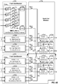
- FIG. 3 shows a block diagram of an exemplary design of wireless device 110 in FIG. 1 .
- wireless device 110 includes a front-end module 320 coupled to a primary antenna 310, a front-end module 322 coupled to a secondary antenna 312, a back-end module 370, and a data processor/controller 380.
- front-end module 320 includes an antenna interface circuit 324, multiple (K) power amplifiers (PAs) 330a to 330k, and multiple (K) MIMO LNAs 340pa to 340pk to support multiple bands, carrier aggregation, multiple radio technologies, etc.
- Front-end module 322 includes an antenna interface circuit 326 and multiple (L) MIMO LNAs 340sa to 340sl to support multiple bands, carrier aggregation, multiple radio technologies, receive diversity, MIMO transmission from multiple transmit antennas to multiple receive antennas, etc.
- Antenna interface circuit 324 may obtain a received RF signal from antenna 310 and may provide one or more input RF signals to one or more MIMO LNAs 340. Antenna interface circuit 324 may also receive an output RF signal from one power amplifier 330 and may provide the output RF signal to antenna 310. Antenna interface circuit 324 may include switches, duplexers, transmit filters, receive filters, matching circuits, etc. Antenna interface circuit 326 may obtain a received RF signal from antenna 312 and may provide one or more input RF signals to one or more MIMO LNAs 340. Antenna interface circuit 326 may include switches, receive filters, matching circuits, etc.
- Each MIMO LNA 340 includes (i) N inputs that can receive up to N input RF signals from antenna interface circuit 324 or 326 and (ii) M outputs that can provide up to M amplified RF signals to back-end module 370, where N > 1 and M > 1.
- MIMO LNA 340pa to 340pk and MIMO LNAs 340sa to 340sl may include the same or different numbers of inputs and may also include the same or different numbers of outputs.
- N and M may be the same for all MIMO LNAs 340 or different for different MIMO LNAs 340.
- a MIMO LNA with N inputs and M outputs may be referred to as an N ⁇ M M MIMO LNA.
- MIMO LNAs 340 may be used to receive transmissions on multiple carriers at different frequencies.
- a MIMO LNA is different from LNAs used to receive a MIMO transmission sent from multiple transmit antennas to multiple receive antennas.
- An LNA for a MIMO transmission typically has (i) one input receiving one input RF signal from one receive antenna and (ii) one output providing one amplified RF signal.
- the multiple outputs of a MIMO LNA thus cover frequency dimension whereas the outputs of LNAs used for a MIMO transmission cover spatial dimension.
- Each MIMO LNA 340 may operate in a single-output mode, an intra-band CA mode, an inter-band same band group CA mode, or an inter-band different band groups CA mode at any given moment.
- the single-output mode may be used to receive a transmission sent on a single carrier without carrier aggregation or transmissions sent on multiple carriers with carrier aggregation.
- a MIMO LNA operates in a 1 ⁇ 1 configuration, receives one input RF signal comprising one or more transmissions on one set of carriers in one band, and provides one amplified RF signal.
- the MIMO LNA In the intra-band CA mode, the MIMO LNA operates in a 1 ⁇ M configuration, receives one input RF signal comprising multiple transmissions on M sets of carriers in the same band, and provides M amplified RF signals for the M sets of carriers.
- the MIMO LNA In the inter-band same band group CA mode, the MIMO LNA operates in an N ⁇ M configuration, receives N input RF signals comprising multiple transmissions on M sets of carriers in up to N bands, and provides M amplified RF signals for the M sets of carriers.
- Each set of carriers may include one or more carriers.
- Each carrier may have a bandwidth of 1.4, 3, 5, 10, 15 or 20 MHz in LTE.
- Back-end module 370 includes various circuits to condition signals for transmission via antenna 310, such as amplifiers, filters, upconverters, matching circuits, oscillators, local oscillator (LO) generators, phase-locked loops (PLL), etc. Back-end module 370 also includes various circuits to condition signals received via antennas 310 and 312, such as downconverters, filters, amplifiers, matching circuits, oscillators, LO generators, PLLs, etc. Back-end module 370 also includes switches and signal traces to interconnect MIMO LNAs 340 to downconverters within back-end module 370, as described below. Back-end module 370 may also be referred to as a transceiver module.
- Front-end modules 320 and 322 and back-end module 370 may be implemented in various manners.
- modules 320, 322 and 370 may each be implemented on one or more analog integrated circuit (ICs), RF ICs (RFICs), mixed-signal ICs, circuit modules, etc.
- modules 320, 322 and 370 may each be implemented on a separate RFIC or circuit module.
- Antenna interface circuits 324 and 326 may be implemented on (i) the same ICs or circuit modules as PAs 330 and LNAs 340 or (ii) separate ICs or circuit modules.
- Front-end modules 320 and 322 and back-end module 370 may also be implemented in other manners.
- Data processor/controller 380 may perform various functions for wireless device 110. For example, data processor 380 may perform processing for data being received by wireless device 110 and data being transmitted by wireless device 110. Controller 380 may control the operation of various circuits in front-end modules 320 and 322 and back-end module 370. A memory 382 may store program codes and data for data processor/controller 380. Data processor/controller 380 may be implemented on one or more application specific integrated circuits (ASICs) and/or other ICs.
- ASICs application specific integrated circuits
- Wireless device 110 may support a number of bands and may also support carrier aggregation.
- antenna interface circuits 324 and 324 may provide a large number of input RF signals for all supported bands and for carrier aggregation.
- Implementing antenna interface circuit 324 and MIMO LNAs 340pa to 340pk together on the same front-end module 320 may avoid the need for RF interconnections between antenna interface circuit 324 and MIMO LNAs 340.
- implementing antenna interface circuit 326 and MIMO LNAs 340sa to 340sk together on the same front-end module 322 may avoid the need for RF interconnections between antenna interface circuit 326 and MIMO LNAs 340.
- MIMO LNAs 340 in front-end modules 320 and 322 instead of back-end module 370, there may be a large number of RF interconnections between front-end modules 320 and 322 and back-end module 370, or more specifically, between MIMO LNAs 340 and back-end module 370. This may then require a large number of input/output (I/O) pins on front-end modules 320 and 322 and back-end module 370. The number of I/O pins may increase in proportion to the number of LNAs interfacing with antenna interface circuits 324 and 326. As a result, package area of front-end modules 320 and 322, die area of back-end module 370, and routing area of a printed circuit board (PCB) containing front-end modules 320 and 322 and back-end module 370 may increase significantly.
- PCB printed circuit board
- the carrier aggregation receiver architecture described herein may provide various advantages.
- First, the receiver architecture may reduce the number of RF interconnections between front-end modules 322 and 322 and back-end module 370, which may then reduce the number of I/O pins on modules 320, 322 and 370.
- Second, the receiver architecture may reduce package area of front-end modules 320 and 322, die area of back-end module 370, and routing area of a PCB containing modules 320, 322 and 370.
- wireless device 110 may simultaneously receive transmissions on up to two sets of carriers in up to two band groups. Each set of carriers may include one or more carriers on which transmissions can be sent to wireless device 110. Wireless device 110 may perform downconversion separately for each set of carriers on which transmissions are sent to wireless device 110. Furthermore, wireless device 110 may perform downconversion separately for each antenna. For example, wireless device 110 may receive transmissions on two sets of carriers via two antennas 310 and 312. Wireless device 110 may then perform downconversion separately for (i) a first set of carriers for primary antenna 310, (ii) the first set of carriers for secondary antenna 312, (iii) a second set of carriers for primary antenna 310, and (iv) the second set of carriers for secondary antenna 312.
- Wireless device 110 may perform downconversion for the first set of carriers for both antennas 310 and 312 using LO signals at a first frequency, which may be determined based on the center frequencies of the carriers in the first set. Wireless device 110 may perform downconversion for the second set of carriers for both antennas 310 and 312 using LO signals at a second frequency, which may be determined based on the center frequencies of the carriers in the second set.
- FIG. 4A shows a schematic diagram of front-end modules 320a and 322a and back-end module 370a, which are one exemplary design of front-end modules 320 and 322 and back-end module 370 in FIG. 3 .
- front-end module 320a includes three MIMO LNAs 440pa, 440pb and 440pc for primary antenna 320 for low-band, mid-band, and high-band, respectively.
- Front-end module 322a includes three MIMO LNAs 440sa, 440sb and 440sc for secondary antenna 322 for low-band, mid-band, and high-band, respectively.
- MIMO LNAs 440 are one exemplary design of MIMO LNAs 340 in FIG. 3 .
- MIMO LNA 440pa is a 4 ⁇ 2 MIMO LNA with four inputs and two outputs.
- MIMO LNA 440pa includes four gain circuits 442a to 442d, eight cascode transistors 444a to 444d and 446a to 446d, and two load circuits 448a and 448b.
- Each gain circuit 442 may be implemented with a transistor having its gate receiving an input RF signal, its sources coupled to circuit ground directly or via a source degeneration inductor, and its drain coupled to the output of the gain circuit.
- Gain circuits 442a to 442d may be used for four bands in low-band and may be coupled to four duplexers or matching circuits within antenna interface circuit 324, which may provide one or two input RF signals to one or two of gain circuits 442a to 442d.
- Cascode transistors 444a to 444d have their sources coupled to the output of gain circuits 442a to 442d, respectively, and their drains coupled to load circuit 448a.
- Cascode transistors 446a to 446d have their sources coupled to the output of gain circuits 442a to 442d, respectively, and their drains coupled to load circuit 448b.
- Cascode transistors 444a to 444d and 446a to 446d receive different control signals, and each cascode transistor 444 or 446 may be turned on or off based on its control signal.
- Load circuit 448a provides a first amplified RF signal for a first set of carriers in low-band.
- Load circuit 448b provides a second amplified RF signal for a second set of carriers in low-band.
- MIMO LNAs 440pa in FIG. 4A may provide various advantages. First, by combining the cascode transistors for each carrier set, the number of LNA outputs may be greatly reduced from eight to two. This may greatly reduce the number of I/O pins required to interface front-end modules 320 and 322 with back-end module 370. Second, each MIMO LNA 440 in FIG. 4A may provide its outputs to back-end module 370 instead of another front-end module. This may improve performance.
- FIG. 4A shows an exemplary design of 4 ⁇ 2 MIMO LNA 440pa.
- an N ⁇ M MIMO LNA with N inputs and M outputs may be implemented with N gain circuits, up to N*M cascode transistors, and M load circuits.
- the cascode transistors may be used to interconnect the N gain circuits to the M load circuits.
- Full interconnection may be obtained by using N*M cascode transistors to connect each gain circuit to each load circuit.
- Partial interconnection may be obtained by connecting a subset of the gain circuits (instead of all N gain circuits) to each load circuit.
- MIMO LNAs 440pb, 440pc, 440sa, 440sb and 440sc may be implemented in similar manner as MIMO LNA 440pa in FIG. 4A .
- the N ⁇ M dimension of each MIMO LNA 440 may be dependent on various factors such as the number of bands supported in each band group, the number of sets of carriers on which transmissions may be sent simultaneously to wireless device 100, the number of available I/O pins, etc.
- MIMO LNAs 440pa, 440pc, 440sa and 440sc are 4x2 MIMO LNAs
- MIMO LNAs 440pb and 440sb are 6x2 MIMO LNAs.
- MIMO LNAs 440 may also have other dimensions.
- back-end module 370a includes six pairs of switches 468 for the six MIMO LNAs 440.
- Switches 468a1, 468b1 and 468c1 have one end coupled to node A1 and the other end coupled to the first output of MIMO LNAs 440pa, 440pb and 440pc, respectively.
- Switches 468a2, 468b2 and 468c2 have one end coupled to node A2 and the other end coupled to the second output of MIMO LNAs 440pa, 440pb and 440pc, respectively.
- Switches 468d1, 468e1 and 468f1 have one end coupled to node B1 and the other end coupled to the first output of MIMO LNAs 440sa, 440sb and 440sc, respectively.
- Switches 468d2, 468e2 and 468f2 have one end coupled to node B2 and the other end coupled to the second output of MIMO LNAs 440sa, 440sb and 440sc, respectively.
- switches 468 are implemented on back-end module 370a. It may be desirable to implement switches 468 on back-end module 370a since the switches may help with impedance matching between front-end modules 320 and 322 and back-end module 370a, e.g., if 50-ohm transmission lines are used between front-end modules 320 and 322 and back-end module 370a.
- the outputs of front-end modules 320 and 322 may be designed as 50-ohm outputs.
- switches 468 are implemented on front-end modules 320 and 322 (instead of back-end module 370). This may reduce the number of RF interconnections between front-end modules 320 and 322 and back-end module 370. For example, the number of RF connections between front-end modules 320 and 322 and back-end module 370 may be reduced from 12 (as shown in FIG. 4A) to 4 (not shown in FIG. 4A ) by implementing switches 468 on front-end modules 320 and 322.
- back-end module 370a further includes two pairs of downconverters, which includes a first pair of downconverters 470a1 and 470b1 for a first set of carriers (or a first carrier set) and a second pair of downconverters 470a2 and 470b2 for a second set of carriers (or a second carrier set).
- Each pair of downconverters includes one downconverter 470a for primary antenna 310 and another downconverter 470b for secondary antenna 312.
- Wireless device 110 may simultaneously receive transmissions on up to two sets of carriers in up to two band groups.
- Up to two pairs of downconverters 470 may be used to perform downconversion for up to two sets of carriers, one pair of downconverters 470 for each set of carriers.
- Each enabled pair of downconverters 470 receives two amplified RF signals from two MIMO LNAs 440 coupled to two antennas 310 and 312 and separately downconverts the two amplified RF signals with two LO signals at the same frequency.
- Downconverters 470a1 and 470b1 perform downconversion for the first carrier set in low-band, mid-band, or high-band.
- Switch 468a1, 468b1 or 468c1 is closed to route an amplified RF signal from the first output of MIMO LNA 440pa, 440pb or 440pc to downconverter 470a1.
- Switch 468d1, 468e1 or 468f1 is closed to route an amplified RF signal from the first output of MIMO LNA 440sa, 440sb or 440sc to downconverter 470b1.
- Downconverters 470a2 and 470b2 perform downconversion for the second carrier set in low-band, mid-band, or high-band.
- Switch 468a2, 468b2 or 468c2 is closed to route an amplified RF signal from the second output of MIMO LNA 440pa, 440pb or 440pc to downconverter 470a2.
- Switch 468d2, 468e2 or 468f2 is closed to route an amplified RF signal from the second output of MIMO LNA 440sa, 440sb or 440sc to downconverter 470b2.
- back-end module 370a further includes (i) lowpass filters 472a1 and 472b1 for downconverters 470a1 and 470b1 for the first carrier set and (ii) lowpass filters 472a2 and 472b2 for downconverters 470a2 and 470b2 for the second carrier set.
- Lowpass filter 472a receives and filters a downconverted signal from downconverter 470a1 and provides an output baseband signal for the first carrier set for primary antenna 310.
- Lowpass filter 472b receives and filters a downconverted signal from downconverter 470b1 and provides an output baseband signal for the first carrier set for secondary antenna 312.
- Lowpass filter 472a2 receives and filters a downconverted signal from downconverter 470a2 and provides an output baseband signal for the second carrier set for primary antenna 310.
- Lowpass filter 472b2 receives and filters a downconverted signal from downconverter 470b2 and provides an output baseband signal for the second carrier set for secondary antenna 312.
- Lowpass filters 472a1 and 472b1 may have a fixed bandwidth or a configurable bandwidth, which may be dependent on the bandwidths of the carriers in the first carrier set.
- Lowpass filters 472a2 and 472b2 may also have a fixed bandwidth or a configurable bandwidth, which may be dependent on the bandwidths of the carriers in the second carrier set.
- back-end module 370a further includes (i) a PLL 480a, a voltage-controlled oscillator (VCO) 482a, and an LO generator 484a for the first carrier set and (ii) a PLL 480b, a VCO 482b, and an LO generators 484b for the second carrier set.
- Each PLL 480 may include a phase-frequency detector, a charge pump, a loop filter, a frequency divider, etc.
- Each LO generator 484 may include a frequency divider, buffers, etc.
- VCO 482a generates a first VCO signal at a first VCO frequency, which may be determined based on the frequencies of the carriers in the first carrier set.
- PLL 480a provides a first control signal to adjust the oscillation frequency of VCO 482a so that the first VCO frequency is at a target frequency for the first carrier set. This target frequency may be dependent on the frequencies of the carriers in the first carrier set, which may in turn be dependent on whether the first carrier set is in low-band, mid-band, or high-band.
- LO generator 484a receives the first VCO signal from VCO 482a and provides LO signals to downconverters 470a1 and 470b1.
- VCO 482b generates a second VCO signal at a second VCO frequency, which may be determined based on the frequencies of the carriers in the second carrier set.
- PLL 480b provides a second control signal to adjust the oscillation frequency of VCO 482b so that the second VCO frequency is at a target frequency for the second carrier set. This target frequency may be dependent on the frequencies of the carriers in the second carrier set, which may in turn be dependent on whether the second carrier set is in low-band, mid-band, or high-band.
- LO generator 484b receives the second VCO signal from VCO 482b and provides LO signals to downconverters 470a2 and 470b2.
- each downconverter pair includes two downconverters 470 for two antennas 310 and 312 for one carrier set in one band.
- the two downconverters 470 in each pair receive LO signals at the same frequency from an associated LO generator 484.
- the two downconverters 470 in each pair are placed close together in order to shorten the routing of the LO signals from the associated LO generator 484.
- the two downconverters 470 in each pair receive two amplified RF signals from two MIMO LNAs 440.
- One or both amplified RF signals for each downconverter pair may be routed via a relatively long signal trace in order to reach the downconverters.
- downconverters 470a1 and 470b1 are for the first carrier set and are placed close together in order to shorten the signal traces from LO generator 484a to downconverters 470a1 and 470b1.
- a first amplified RF signal from MIMO LNA 440pa for primary antenna 310 may be routed over a relatively long signal trace to downconverter 470a1.
- a second amplified RF signal from MIMO LNA 440sa for secondary antenna 312 may be routed over a relatively short signal trace to downconverter 470b 1.
- the closeness of the two downconverters 470 in each pair of downconverters may be quantified in various manners.
- the two downconverters 470 in each pair may be placed closer than a predetermined distance, which may be selected to obtain good performance, e.g., sufficiently low power consumption for LO generators 484.
- the routing distance d LO of the LO signals from the LO generator to the downconverters may be shorter than (i) the routing distance d SIG1 of the first amplified RF signal provided to a first downconverter in the pair and/or (ii) the routing distance d SIG2 of the second amplified RF signal provided to a second downconverter in the pair.
- the closeness of the two downconverters 470 in each pair may also be quantified in other manners.
- each pair of downconverters 470 sharing the same LO generator 484 close to each other may reduce the signal traces for the LO signals from LO generator 484 to downconverters 470.
- the shorter signal traces for the LO signals may provide various advantages such as reduced power consumption of LO generators 484, less radiation of the LO signals, etc.
- back-end module 370a may be symmetric about line XY.
- the circuits within back-end module 370a may be fabricated on an IC die.
- the entire IC die may be used for a wireless device supporting carrier aggregation on two antennas.
- the IC die may be split at line XY. Each half of the IC die can support operation via a single antenna without receive diversity. Each half of the IC die may be used for a wireless device not supporting receive diversity.
- FIG. 4B shows a schematic diagram of front-end modules 320b and 322b, which are another exemplary design of front-end modules 320 and 322 in FIG. 3 .
- Front-end module 320b includes three MIMO LNAs 440pa, 440pb and 440pc for primary antenna 310 for low-band, mid-band, and high-band, respectively.
- Front-end module 322b includes three MIMO LNAs 440sa, 440sb and 440sc for secondary antenna 312 for low-band, mid-band, and high-band, respectively.
- MIMO LNA 440pa for low-band includes four gain circuits 442a to 442d, eight cascode transistors 444a to 444d and 446a to 446d, and two load circuits 448a and 448b, which are coupled as described above for FIG. 4A .
- Gain circuits 452a to 452n may be coupled to N duplexers or matching circuits within antenna interface circuit 324, which may provide one or two input RF signals to one or two of gain circuits 452a to 452n.
- Cascode transistors 454a to 454n have their sources coupled to the output of gain circuits 452a to 452n, respectively, and their drains coupled to load circuit 458a.
- Cascode transistors 456a to 456n have their sources coupled to the output of gain circuits 452a to 452n, respectively, and their drains coupled to load circuit 458b. Cascode transistors 454a to 454n and 456a to 456n receive different control signals, and each cascode transistor 454 or 456 may be turned on or off based on its control signal.
- Load circuit 458a provides a first amplified RF signal for a first set of at least one carrier in mid-band.
- Load circuit 458b provides a second amplified RF signal for a second set of at least one carrier in mid-band.
- a cascode transistor 460a has its source coupled to the output of gain circuit 452a within MIMO LNA 440pb, its gate receiving a control signal, and its drain coupled to load circuit 448a within MIMO LNA 440pa.
- Cascode transistor 460 functions as a port expander switch that can route an RF signal from MIMO LNA 440pb for mid-band to MIMO LNA 440pa for low-band.
- Gain circuit 452a within MIMO LNA 440pb may be operated at low-band and may provide its amplified RF signal via cascode transistor 460a to load circuit 448a within MIMO LNA 440pa.
- a cascode transistor 460b may be coupled between MIMO LNAs 440sa and 440sb and may act as a port expander for MIMO LNA 460sa.
- one or more port expanders may be used between any pair of MIMO LNAs.
- Each port expander may be coupled between a gain circuit in one MIMO LNA and a load circuit in another MIMO LNA.
- More port expanders may be used to effectively increase the number of ports of a MIMO LNA.
- FIG. 5 shows a schematic diagram of back-end module 370b, which is another exemplary design of back-end module 370 in FIG. 3 .
- back-end module 370b includes six pairs of downconverters (DC) 470, as follows:
- Downconverters 470a1, 470c1 and 470e1 are for primary antenna 310 for low-band, mid-band, and high-band, respectively, and have their outputs coupled together and to the input of lowpass filter 472a1.
- downconverters 470b1, 470d1 and 470f1 are for secondary antenna 312 for low-band, mid-band, and high-band, respectively, and have their outputs coupled together and to the input of lowpass filter 472b1.
- Lowpass filter 472a1 receives and filters a downconverted signal from downconverters 470a1, 470c1 or 470e1 and provides an output baseband signal for the first carrier set for primary antenna 310.
- lowpass filter 472b1 receives and filters a downconverted signal from downconverters 470b1, 470d1 or 470f1 and provides an output baseband signal for the first carrier set for secondary antenna 312.
- Each lowpass filter 472 may have a fixed bandwidth or a configurable bandwidth, which may be dependent on the bandwidths of the carriers in the first carrier set.
- Lowpass filter 472a2 and 472b2 are coupled to downconverters 470a2 to 470f2 in the same way that lowpass filter 472a1 and 472b1 are coupled to downconverters 470a1 to 470f1.
- Lowpass filter 472a2 receives and filters a downconverted signal from downconverters 470a2, 470c2 or 470e2 and provides an output baseband signal for the second carrier set for primary antenna 310.
- lowpass filter 472b2 receives and filters a downconverted signal from downconverters 470b2, 470d2 or 470f2 and provides an output baseband signal for the second carrier set for secondary antenna 312.
- VCO 482a generates a first VCO signal at a first VCO frequency and is controlled by PLL 480a.
- LO generator 484a1 generates LO signals at a first frequency for downconverters 470a1 and 470b1.
- LO generator 484b1 generates LO signals at a second frequency for downconverters 470c1 and 470d1.
- LO generator 484c1 generates LO signals at a third frequency for downconverters 470e1 and 470f1.
- VCO 482b generates a second VCO signal at a second VCO frequency and is controlled by PLL 480b.
- LO generator 484a2 generates LO signals at a fourth frequency for downconverters 470a2 and 470b2.
- LO generator 484b2 generates LO signals at a fifth frequency for downconverters 470c2 and 470d2.
- LO generator 484c2 generates LO signals at a sixth frequency for downconverters 470e
- FIG. 6 shows a schematic diagram of an exemplary design of a back-end module 372.
- back-end module 372 includes MIMO LNAs 440pa, 440pb, 440pc, 440sa, 440sb and 440sc, switches 468, and all of the circuits in back-end module 370a in FIG. 4A .
- Integrating MIMO LNAs 440 and downconverters 470 within the same back-end module 372 may provide certain advantages such as improved performance, higher level of integration, lower cost, etc.
- Back-end module 372 may be coupled to one or more front-end modules.
- back-end module 372 may be coupled to (i) a first front-end module including an antenna interface circuit and power amplifiers for a primary antenna and (ii) a second front-end module including an antenna interface circuit for a secondary antenna. In another exemplary design, back-end module 372 may be coupled to a single front-end module including antenna interface circuits for both primary and secondary antennas and power amplifiers.
- back-end module 372 may be symmetric about line XY.
- the circuits within back-end module 372 may be fabricated on an IC die.
- the IC die may be split at line XY.
- Each half of the IC die may include one half of the MIMO LNAs and one half of the downconverters.
- Each half of the IC die can support operation via a single antenna without receive diversity.
- This symmetric layout of back-end module 372 may provide certain advantages such as savings in design effort and faster to time to market based on good upfront planning.
- FIGS. 3 to 5 show an exemplary design in which MIMO LNAs are implemented on front-end modules.
- FIG. 6 shows an exemplary design in which MIMO LNAs are implemented on a back-end module.
- This exemplary design may result in more RF routing between the front-end modules and the back-end module depending on the number of inputs and the number of outputs of each MIMO LNA.
- the outputs of the MIMO LNAs may be coupled to downconverters as shown in FIGS. 4A , 4B , 5 or 6 to obtain the advantages described below.
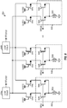
- FIG. 7 shows a schematic diagram of an exemplary design of an N ⁇ 2 MIMO LNA 440x based on a split cascode architecture.
- MIMO LNA 440x may be used for each of MIMO LNA 440 in FIGS. 4A to 6 .
- MIMO LNA 440x includes N gain circuits 742a to 742n coupled to N LNA inputs, 2N cascode transistors 744a to 744n and 746a to 746n, and two load circuits 748a and 748b coupled to two LNA outputs.
- Gain circuit 742a includes an N-channel metal oxide semiconductor (NMOS) transistor 754a having its gate receiving a first input RF signal (RFin1) via one LNA input and its source coupled to one end of a source degeneration inductor 752a. The other end of inductor 752a is coupled to circuit ground.
- Two cascode transistors 744a and 746a are coupled between gain circuit 742a and load circuits 748a and 748b.
- Cascode transistors 744a and 746a have their sources coupled to the drain of gain transistor 754a, their gates receiving control signals Vctrl11 and Vctrl12 respectively, and their drains coupled to load circuits 748a and 748b, respectively.
- Gain circuits 742b to 742n and cascode transistors 744b to 744n and 746b to 746n are coupled in similar manner as gain transistor 742a and cascode transistors 744a and 746a.
- load circuit 748a includes a transformer 762a comprising (i) a primary coil 764a coupled between the drains of cascode transistors 744a to 744n and a power supply, VDD, and (ii) a secondary coil 766a providing a differential first amplified RF signal (RFamp1).
- Load circuit 748b includes a transformer 762b having (i) a primary coil 764b coupled between the drains of cascode transistors 746a to 746n and the VDD supply and (ii) a secondary coil 766b providing a differential second amplified RF signal (RFamp2).
- Load circuits 748 may also be implemented in other manners.
- a load circuit may include an inductor and possibly a capacitor coupled between the VDD supply and the drains of the cascode transistors.
- the cascode transistors may provide the amplified RF signal at their drains.
- a load circuit may include a P-channel metal oxide semiconductor (PMOS) transistor having its source coupled to the VDD supply and its drain coupled to the drains of the cascode transistors.
- the PMOS transistor may provide an active load for one or more cascode transistors.
- MIMO LNA 440x may support a single-output mode, an intra-band CA mode, an inter-band CA mode for the same band group, and an inter-band CA mode for different band groups.
- a single input RF signal may be received via one of the N LNA inputs and applied to a single gain circuit 742.
- This gain circuit 742 is coupled to a single load circuit 748 via a single cascode transistor 744 or 746.
- a single amplified RF signal for one set of carriers is provided by the single load circuit 748 to one LNA output.
- MIMO LNA 440x can support the single-output mode and the inter-band CA mode with an input RF signal applied to any one of the N gain circuits 742.
- a single input RF signal may be received via one of the N LNA inputs and applied to a single gain circuit 742.
- This gain circuit 742 is coupled to both load circuits 748a and 748b via two cascode transistors 744 and 746 coupled to the gain circuit.
- Two amplified RF signals for two sets of carriers are provided by the two load circuits 748a and 748b to the two LNA outputs.
- MIMO LNA 440x can allow an input RF signal to be applied to any gain circuit 742 and routed to any load circuit 748.
- two input RF signals for two bands are received via two of the N LNA inputs and applied to two gain circuits 742.
- One gain circuit 742 is coupled to one load circuit 748 via one cascode transistor 744.
- the other gain circuit 742 is coupled to the other load circuit 748 via another cascode transistor 746.
- Two amplified RF signals for two sets of carriers are provided by two load circuits 748a and 748b to the two LNA outputs.
- FIG. 8 shows a schematic diagram of an exemplary design of an N ⁇ 2 MIMO LNA 440y based on a split gm architecture.
- MIMO LNA 440y may be used for each of MIMO LNA 440 in FIGS. 4A to 6 .
- MIMO LNA 440y includes N gain circuits 842a to 842n coupled to N LNA inputs, 2N cascode transistors 844a to 844n and 846a to 846n, and two load circuits 848a and 848b coupled to two LNA outputs.
- Gain circuit 842a includes two NMOS transistors 854a and 856a having their gates receiving a first input RF signal (RFin1) via one LNA input and their sources coupled to one end of a source degeneration inductor 852a. The other end of inductor 852a is coupled to circuit ground.
- Two cascode transistors 844a and 846a are coupled between gain circuit 842a and load circuits 848a and 848b, respectively.
- Cascode transistors 844a and 846a have their sources coupled to the drains of gain transistors 854a and 856a, respectively, their gates receiving control signals Vctrl11 and Vctrl12 respectively, and their drains coupled to load circuits 848a and 848b, respectively.
- MIMO LNA 440y may support the single-output mode, the intra-band CA mode, the inter-band CA mode for the same band group, and the inter-band CA mode for different band groups, as described above for MIMO LNA 440x in FIG. 7 .
- FIGS. 7 and 8 show two exemplary designs of a MIMO LNA.
- a MIMO LNA may also be implemented in other manners.
- a gain circuit within a MIMO LNA may include a gain transistor having its source coupled directly to circuit ground instead of to a source degeneration inductor.
- FIG. 9 shows an exemplary design of a pair of downconverters 470a and 470b and lowpass filters 472a and 472b, which may be used for any pair of downconverters 470 and associated lowpass filters 472 in FIGS. 4A to 6 .
- Downconverter 470a includes a pair of mixers 972a and 974a that performs quadrature downconversion for an amplified RF signal (RFampp) from a MIMO LNA for primary antenna 310.
- Mixer 972a receives the RFampp signal and an inphase LO signal (ILOa) from LO generator 484, downconverts the RFampp signal with the ILOa signal, and provides an inphase (I) downconverted signal.
- Mixer 974a receives the RFampp signal and a quadrature LO signal (QLOa), downconverts the RFampp signal with the QLOa signal, and provides a quadrature (Q) downconverted signal.
- QLOa quadrature LO signal
- Lowpass filters 472a includes a first lowpass filter 982a for the I path and a second lowpass filter 984a for the Q path.
- Filters 982a and 984a receive and filter the I and Q downconverted signals from mixers 972a and 974a, respectively, and provide I and Q baseband output signals for one set of carriers for primary antenna 310.
- Downconverter 470b includes a pair of mixers 972b and 974b that performs quadrature downconversion for an amplified RF signal (RFamps) from a MIMO LNA for secondary antenna 312.
- Mixers 972b and 974b receive and downconvert the RFamps signal with inphase and quadrature LO signals (ILOb and QLOb) respectively, from LO generator 484, and provide I and Q downconverted signals, respectively.
- Lowpass filters 982b and 984b within lowpass filter 472b receive and filter the I and Q downconverted signals from mixers 972b and 974b, respectively, and provide I and Q baseband output signals for one set of carriers for secondary antenna 312.
- FIG. 9 also shows an exemplary design of LO generator 484, which includes a frequency divider 990 and buffers 992a, 992b, 994a and 994b.
- Divider 990 receives a VCO signal from a VCO 482, divides the VCO signal in frequency by an integer or non-integer ratio, and provides I and Q LO signals at a target frequency for one set of carriers being received.
- the I LO signal is offset from the Q LO signal by 90° at the target frequency.
- the I LO signal is buffered by buffers 992a and 992b to generate ILOa and ILOb signals for mixers 972a and 972b, respectively, within downconverters 472a and 472b.
- the Q LO signal is buffered by buffers 994a and 994b to generate QLOa and QLOb signals for mixers 974a and 974b, respectively, within downconverters 472a and 472b.
- the carrier aggregation receiver architecture disclosed herein may provide various advantages.
- the receiver architecture may support all CA schemes shown in FIGS. 2A to 2D with receive diversity.
- the receiver architecture may use a relatively small number of RF interconnections between front-end modules 320 and 322 and back-end module 370. This may result in a smaller die area for back-end module 370, a smaller package area for front-end modules 320 and 322, and reduced routing area on a PCB that includes front-end modules 320 and 322 and back-end module 370.
- each MIMO LNA may include any number of gain circuits for any number of bands without increasing the number of output pins on front-end modules 320 and 322. This may be especially desirable for wireless devices supporting multiple bands simultaneously.
- a back-end module may include identical circuits for the two sets of carriers, e.g., as shown in FIGS. 4A and 6 .
- An IC die of the back-end module may be physically split into two, and each half may be used for a wireless device to support operation on one set of carriers (i.e., no carrier aggregation) via two antennas. This may be achieved without having to redesign a wireless device not supporting carrier aggregation.
- MIMO LNAs 440 within front-end module 320 may be similar or identical to MIMO LNAs 440 within front-end module 322.
- the output ports of MIMO LNAs 440 may provide amplified RF signals for primary antenna 310 and secondary antenna 312 (instead of amplified RF signals for two sets of carriers).
- MIMO LNAs 440 may be reused to support receive diversity with two antennas instead of carrier aggregation on two sets of carriers.
- an apparatus e.g., a wireless device, an IC, a circuit module, etc.
- a plurality of LNAs may include a plurality of LNAs, a plurality of switches, and at least one downconverter.
- the plurality of LNAs e.g., LNAs 440 in FIG. 4A
- the plurality of switches may be coupled to the outputs of the plurality of LNAs.
- the at least one downconverter (e.g., downconverters 470) may be coupled to the plurality of switches and may downconvert the at least one amplified RF signal and provide at least one downconverted signal.
- the switches may reduce the number of downconverters needed to support reception of transmissions on multiple sets of carriers via multiple receive antennas, e.g., shown by comparing FIG. 4A to FIG. 6 .
- the plurality of LNAs may comprise (i) a first set of LNAs (e.g., LNAs 440pa, 440pb and 440pc) for a first antenna (e.g., primary antenna 310) and (ii) a second set of LNAs (e.g., LNAs 440sa, 440sb and 440sc) for a second antenna (e.g., secondary antenna 312).
- the first set of LNAs may include at least two LNAs for at least two band groups, e.g., three LNAs 440pa, 440pb and 440pc for three band groups of low-band, mid-band, and high-band.
- the second set of LNAs may include at least two additional LNAs for the at least two band groups, e.g., e.g., three LNAs 440sa, 440sb and 440sc for the three band groups of low-band, mid-band, and high-band.
- each of the plurality of LNAs may comprise M outputs and may provide up to M amplified RF signals from up to M outputs, where M may be any integer greater than one.
- each LNA may comprise two outputs and may provide up to two amplified RF signals from up to two outputs for up to two sets of carriers.
- Each LNA may comprise a plurality of gain circuits and a plurality of cascode transistors.
- each gain circuit may comprise a gain transistor (e.g., gain transistor 754 in FIG. 7 ) coupled between an input and an output of the gain circuit.
- the plurality of cascode transistors e.g., cascode transistors 744 and 746 in FIG.
- each gain circuit may comprise first and second gain transistors (e.g., transistors 854 and 856 in FIG. 8 ) coupled between an input and first and second outputs of the gain circuit.
- the plurality of cascode transistors e.g., cascode transistors 844 and 846 in FIG. 8
- cascode transistors 844 and 846 in FIG. 8 may be coupled between the first and second outputs of the plurality of gain circuits and the plurality of load circuits for the LNA.
- the at least one downconverter may include first and second downconverters.
- the first downconverter e.g., downconverter 470a1 in FIG. 4A
- the second downconverter e.g., downconverter 470b1 in FIG. 4A
- the first downconverter may perform downconversion for a first amplified RF signal for the first antenna.
- the second downconverter may perform downconversion for a second amplified RF signal for the second antenna.
- the at least one downconverter may include first to fourth downconverters.
- the plurality of LNAs may each comprise first and second outputs.
- the first downconverter e.g., downconverter 470a1 in FIG. 4A
- the first downconverter may be coupled to the first outputs of the first set of LNAs via a first subset of the plurality of switches (e.g., switches 468a1, 468b1 and 468c1 in FIG. 4A ).
- the second downconverter (e.g., downconverter 470b1) may be coupled to the first outputs of the second set of LNAs via a second subset of the plurality of switches (e.g., switches 468d1, 468e1 and 468f1 in FIG. 4A ).
- the third downconverter (e.g., downconverter 470a2) may be coupled to the second outputs of the first set of LNAs via a third subset of the plurality of switches (e.g., switches 468a2, 468b2 and 468c2 in FIG. 4A ).
- the fourth downconverter (e.g., downconverter 470b2) may be coupled to the second outputs of the second set of LNAs via a fourth subset of the plurality of switches (e.g., switches 468d2, 468e2 and 468f2 in FIG. 4A ).
- the first downconverter may perform downconversion for a first amplified RF signal for the first antenna for a first set of carriers.
- the second downconverter may perform downconversion for a second amplified RF signal for the second antenna for the first set of carriers.
- the third downconverter may perform downconversion for a third amplified RF signal for the first antenna for a second set of carriers.
- the fourth downconverter may perform downconversion for a fourth amplified RF signal for the second antenna for the second set of carriers.
- the wireless device may further include first and second LO generators.
- the first LO generator e.g., LO generator 484a in FIG. 4A
- the second LO generator e.g., LO generator 484b
- the third and fourth downconverters may provide LO signals at a second frequency to the third and fourth downconverters.
- the first and second downconverters may be located close to each other (e.g., located within a predetermined distance of each other) in order to reduce signal routing from the first LO generator to the first and second downconverters.
- the predetermined distance may be quantified by one or more times the length or width dimension of a layout of one downconverter on an IC die.
- the first and second downconverters may be located closer to the first set of LNAs than the second set of LNAs (or vice versa).
- the third and fourth downconverters may be located close to each other (e.g., located within the predetermined distance of each other) in order to reduce signal routing from the second LO generator to the third and fourth downconverters
- the wireless device may further include at least one switch operating as a port expander.
- Each such switch may be implemented with a cascode transistor (e.g., cascode transistor 460a in FIG. 4B ) and may be coupled between two of the plurality of LNAs.
- the wireless device may comprise at least one front-end module and a back-end module.
- the at least one front-end module e.g., front-end modules 320 and 322 in FIG. 3
- the back-end module e.g., back-end module 370
- the back-end module may further comprise the plurality of switches. The switches may be implemented on the front-end module(s) instead of the back-end module.
- the plurality of LNAs, the plurality of switches, and the at least one downconverter may be implemented on the back-end module, e.g., as shown in FIG. 6 .
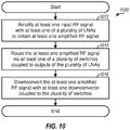
- FIG. 10 shows an exemplary design of a process 1000 for receiving transmissions in a wireless system.
- Process 1000 may be performed by a wireless device or by some other entity.
- At least one input RF signal may be amplified with at least one of a plurality of LNAs to obtain at least one amplified RF signal (block 1012).
- the at least one amplified RF signal may be routed via at least one of a plurality of switches coupled to the outputs of the plurality of LNAs (block 1014).
- the at least one amplified RF signal may be downconverted with at least one downconverter coupled to the plurality of switches (block 1016).
- the plurality of LNAs may comprise a first set of LNAs (e.g., LNAs 440pa, 440pb and 440pc in FIG. 4A ) for a first antenna and a second set of LNAs (e.g., LNAs 440sa, 440sb and 440sc in FIG. 4A ) for a second antenna.
- Each LNA may comprise a first output for a first set of carriers and a second output for a second set of carriers.
- the at least one amplified RF signal may comprise a first amplified RF signal for the first antenna for the first set of carriers, a second amplified RF signal for the second antenna for the first set of carriers, a third amplified RF signal for the first antenna for the second set of carriers, and a fourth amplified RF signal for the second antenna for the second set of carriers.
- the first amplified RF signal may be downconverted with a first downconverter (e.g., downconverter 470a1 in FIG. 4A ) to obtain a first downconverted signal for the first antenna for the first set of carriers.
- the second amplified RF signal may be downconverted with a second downconverter (e.g., downconverter 470b1 in FIG. 4A ) to obtain a second downconverted signal for the second antenna for the first set of carriers.
- the third amplified RF signal may be downconverted with a third downconverter (e.g., downconverter 470a2 in FIG. 4A ) to obtain a third downconverted signal for the first antenna for the second set of carriers.
- the fourth amplified RF signal may be downconverted with a fourth downconverter (e.g., downconverter 470b2 in FIG. 4A ) to obtain a fourth downconverted signal for the second antenna for the second set of carriers.
- the LNAs, switches, downconverters, front-end modules, and back-end modules described herein may be implemented on one or more ICs, analog ICs, RFICs, mixed-signal ICs, PCBs, an electronic device, etc.
- the LNAs, switches, downconverters, front-end modules, and back-end modules may also be fabricated with various IC process technologies such as complementary metal oxide semiconductor (CMOS), NMOS, PMOS, bipolar junction transistor (BJT), bipolar-CMOS (BiCMOS), silicon germanium (SiGe), gallium arsenide (GaAs), heterojunction bipolar transistors (HBTs), high electron mobility transistors (HEMTs), silicon-on-insulator (SOI), etc.
- CMOS complementary metal oxide semiconductor
- NMOS NMOS
- PMOS bipolar junction transistor
- BiCMOS bipolar-CMOS
- SiGe silicon germanium
- GaAs gallium arsenide
- HBTs heterojunction bi
- An apparatus implementing the LNAs, switches, downconverters, front-end modules, and/or back-end modules described herein may be a stand-alone device or may be part of a larger device.
- a device may be (i) a stand-alone IC, (ii) a set of one or more ICs that may include memory ICs for storing data and/or instructions, (iii) an RFIC such as an RF receiver (RFR) or an RF transmitter/receiver (RTR), (iv) an ASIC such as a mobile station modem (MSM), (v) a module that may be embedded within other devices, (vi) a receiver, cellular phone, wireless device, handset, or mobile unit, (vii) etc.
- RFR RF receiver
- RTR RF transmitter/receiver
- MSM mobile station modem
- the functions described may be implemented in hardware, software, firmware, or any combination thereof. If implemented in software, the functions may be stored on or transmitted over as one or more instructions or code on a computer-readable medium.
- Computer-readable media includes both computer storage media and communication media including any medium that facilitates transfer of a computer program from one place to another.
- a storage media may be any available media that can be accessed by a computer.
- such computer-readable media can comprise RAM, ROM, EEPROM, CD-ROM or other optical disk storage, magnetic disk storage or other magnetic storage devices, or any other medium that can be used to carry or store desired program code in the form of instructions or data structures and that can be accessed by a computer.
- any connection is properly termed a computer-readable medium.
- the software is transmitted from a website, server, or other remote source using a coaxial cable, fiber optic cable, twisted pair, digital subscriber line (DSL), or wireless technologies such as infrared, radio, and microwave
- the coaxial cable, fiber optic cable, twisted pair, DSL, or wireless technologies such as infrared, radio, and microwave are included in the definition of medium.
- Disk and disc includes compact disc (CD), laser disc, optical disc, digital versatile disc (DVD), floppy disk and blu-ray disc where disks usually reproduce data magnetically, while discs reproduce data optically with lasers. Combinations of the above should also be included within the scope of computer-readable media.
Description
- The present disclosure relates generally to electronics, and more specifically to a receiver architecture for a wireless device.
- A wireless device (e.g., a cellular phone or a smartphone) in a wireless communication system may transmit and receive data for two-way communication. The wireless device may include a transmitter for data transmission and a receiver for data reception. For data transmission, the transmitter may modulate a radio frequency (RF) carrier signal with data to obtain a modulated RF signal, amplify the modulated RF signal to obtain an output RF signal having the proper output power level, and transmit the output RF signal via an antenna to a base station. For data reception, the receiver may obtain a received RF signal via the antenna and may amplify and process the received RF signal to recover data sent by the base station.
- A wireless device may support carrier aggregation, which is simultaneous operation on multiple carriers. A carrier may refer to a range of frequencies used for communication and may be associated with certain characteristics. For example, a carrier may be associated with system information describing operation on the carrier. A carrier may also be referred to as a component carrier (CC), a frequency channel, a cell, etc. It is desirable to efficiently support carrier aggregation by the wireless device.
- Document
WO 2005/088847 A1 refers to a multimode/multiband mobile station and a method for operating the same. A transmission module transmits multimode/multiband signals through transmitters. A reception module receives radio signals for different services of the same frequency band among multimode/multiband signals through receivers for the same frequency band, and receives radio signals of different frequency bands among the multimode/multiband signals through receivers for the different frequency bands. The multimode/multiband mobile station can reduce the number of receivers by making use of one receiver to receive radio signals for different services of the same frequency band. The multimode/multiband mobile station can use a duplexer of the conventional frequency division duplex (FDD) technique (e.g., wideband code division multiple access (WCDMA)) in a time division duplex (TDD) technique (e.g., Global System for Mobile Communication (GSM) 850 or Personal Communication Service (PCS) 1900). - In accordance with the present invention, an apparatus as set forth in
claim 1, and a method as set forth in claim 14 are provided. Further embodiments of the invention are claimed in the dependent claims. -
-
FIG. 1 shows a wireless device communicating with a wireless system. -
FIGS. 2A to 2D show four examples of carrier aggregation (CA). -
FIG. 3 shows a block diagram of the wireless device inFIG. 1 . -
FIGS. 4A to 6 show some exemplary designs of front-end and back-end modules within the wireless device. -
FIGS. 7 and8 show two exemplary designs of a multiple-input multiple-output (MIMO) low noise amplifier (LNA). -
FIG. 9 shows an exemplary design of a pair of downconverters. -
FIG. 10 shows a process for receiving transmissions in a wireless system. - The detailed description set forth below is intended as a description of exemplary designs of the present disclosure and is not intended to represent the only designs in which the present disclosure can be practiced. The term "exemplary" is used herein to mean "serving as an example, instance, or illustration." Any design described herein as "exemplary" is not necessarily to be construed as preferred or advantageous over other designs. The detailed description includes specific details for the purpose of providing a thorough understanding of the exemplary designs of the present disclosure. It will be apparent to those skilled in the art that the exemplary designs described herein may be practiced without these specific details. In some instances, well-known structures and devices are shown in block diagram form in order to avoid obscuring the novelty of the exemplary designs presented herein.
- A receiver architecture suitable for carrier aggregation and having various advantages is disclosed herein. The receiver architecture may be used for various types of electronic devices such as wireless communication devices.
-
FIG. 1 shows awireless device 110 capable of communicating with awireless communication system 120.Wireless system 120 may be a Long Term Evolution (LTE) system, a Code Division Multiple Access (CDMA) system, a Global System for Mobile Communications (GSM) system, a wireless local area network (WLAN) system, or some other wireless system. A CDMA system may implement Wideband CDMA (WCDMA), Time Division Synchronous CDMA (TD-SCDMA), cdma2000, or some other version of CDMA. For simplicity,FIG. 1 showswireless system 120 including twobase stations system controller 140. In general, a wireless system may include any number of base stations and any set of network entities. -
Wireless device 110 may also be referred to as a user equipment (UE), a mobile station, a terminal, an access terminal, a subscriber unit, a station, etc.Wireless device 110 may be a cellular phone, a smartphone, a tablet, a wireless modem, a personal digital assistant (PDA), a handheld device, a laptop computer, a smartbook, a netbook, a cordless phone, a wireless local loop (WLL) station, a Bluetooth device, etc.Wireless device 110 may be capable of communicating withwireless system 120.Wireless device 110 may also be capable of receiving signals from broadcast stations (e.g., a broadcast station 134), signals from satellites (e.g., a satellite 150) in one or more global navigation satellite systems (GNSS), etc.Wireless device 110 may support one or more radio technologies for wireless communication such as LTE, cdma2000, WCDMA, TD-SCDMA, GSM, 802.11, etc. -
Wireless device 110 may support carrier aggregation, which is operation on multiple carriers. Carrier aggregation may also be referred to as multi-carrier operation.Wireless device 110 may be able to operate in low-band from 698 to 960 megahertz (MHz), mid-band from 1475 to 2170 MHz, and/or high-band from 2300 to 2690 and 3400 to 3800 MHz. Low-band, mid-band, and high-band refer to three groups of bands (or band groups), with each band group including a number of frequency bands (or simply, "bands"). Each band may cover up to 200 MHz and may include one or more carriers. Each carrier may cover up to 20 MHz in LTE. LTE Release 11 supports 35 bands, which are referred to as LTE/UMTS bands and are listed in 3GPP TS 36.101.Wireless device 110 may be configured with up to 5 carriers in one or two bands in LTE Release 11. - In general, carrier aggregation (CA) may be categorized into two types - intra-band CA and inter-band CA. Intra-band CA refers to operation on multiple carriers within the same band. Inter-band CA refers to operation on multiple carriers in different bands.
-
FIG. 2A shows an example of contiguous intra-band CA. In the example shown inFIG. 2A ,wireless device 110 is configured with four contiguous carriers in the same band, which is a band in low-band.Wireless device 110 may send and/or receive transmissions on multiple contiguous carriers within the same band. -
FIG. 2B shows an example of non-contiguous intra-band CA. In the example shown inFIG. 2B ,wireless device 110 is configured with four non-contiguous carriers in the same band, which is a band in low-band. The carriers may be separated by 5 MHz, 10 MHz, or some other amount.Wireless device 110 may send and/or receive transmissions on multiple non-contiguous carriers within the same band. -
FIG. 2C shows an example of inter-band CA in the same band group. In the example shown inFIG. 2C ,wireless device 110 is configured with four carriers in two bands in the same band group, which is low-band.Wireless device 110 may send and/or receive transmissions on multiple carriers in different bands in the same band group (e.g., low-band inFIG. 2C ). -
FIG. 2D shows an example of inter-band CA in different band groups. In the example shown inFIG. 2D ,wireless device 110 is configured with four carriers in two bands in different band groups, which include two carriers in one band in low-band and two additional carriers in another band in mid-band.Wireless device 110 may send and/or receive transmissions on multiple carriers in different bands in different band groups (e.g., low-band and mid-band inFIG. 2D ). -
FIGS. 2A to 2D show four examples of carrier aggregation. Carrier aggregation may also be supported for other combinations of bands and band groups. For example, carrier aggregation may be supported for low-band and high-band, mid-band and high-band, high-band and high-band, etc. -
FIG. 3 shows a block diagram of an exemplary design ofwireless device 110 inFIG. 1 . In this exemplary design,wireless device 110 includes a front-end module 320 coupled to aprimary antenna 310, a front-end module 322 coupled to asecondary antenna 312, a back-end module 370, and a data processor/controller 380. - In the exemplary design shown in
FIG. 3 , front-end module 320 includes anantenna interface circuit 324, multiple (K) power amplifiers (PAs) 330a to 330k, and multiple (K) MIMO LNAs 340pa to 340pk to support multiple bands, carrier aggregation, multiple radio technologies, etc. Front-end module 322 includes anantenna interface circuit 326 and multiple (L) MIMO LNAs 340sa to 340sl to support multiple bands, carrier aggregation, multiple radio technologies, receive diversity, MIMO transmission from multiple transmit antennas to multiple receive antennas, etc. -
Antenna interface circuit 324 may obtain a received RF signal fromantenna 310 and may provide one or more input RF signals to one or more MIMO LNAs 340.Antenna interface circuit 324 may also receive an output RF signal from one power amplifier 330 and may provide the output RF signal toantenna 310.Antenna interface circuit 324 may include switches, duplexers, transmit filters, receive filters, matching circuits, etc.Antenna interface circuit 326 may obtain a received RF signal fromantenna 312 and may provide one or more input RF signals to one or more MIMO LNAs 340.Antenna interface circuit 326 may include switches, receive filters, matching circuits, etc. - Each MIMO LNA 340 includes (i) N inputs that can receive up to N input RF signals from
antenna interface circuit end module 370, where N > 1 and M > 1. MIMO LNA 340pa to 340pk and MIMO LNAs 340sa to 340sl may include the same or different numbers of inputs and may also include the same or different numbers of outputs. Hence, N and M may be the same for all MIMO LNAs 340 or different for different MIMO LNAs 340. A MIMO LNA with N inputs and M outputs may be referred to as an N × M MIMO LNA. - MIMO LNAs 340 may be used to receive transmissions on multiple carriers at different frequencies. A MIMO LNA is different from LNAs used to receive a MIMO transmission sent from multiple transmit antennas to multiple receive antennas. An LNA for a MIMO transmission typically has (i) one input receiving one input RF signal from one receive antenna and (ii) one output providing one amplified RF signal. The multiple outputs of a MIMO LNA thus cover frequency dimension whereas the outputs of LNAs used for a MIMO transmission cover spatial dimension.
- Each MIMO LNA 340 may operate in a single-output mode, an intra-band CA mode, an inter-band same band group CA mode, or an inter-band different band groups CA mode at any given moment. The single-output mode may be used to receive a transmission sent on a single carrier without carrier aggregation or transmissions sent on multiple carriers with carrier aggregation. In the single-output mode or the inter-band different band groups CA mode, a MIMO LNA operates in a 1×1 configuration, receives one input RF signal comprising one or more transmissions on one set of carriers in one band, and provides one amplified RF signal. In the intra-band CA mode, the MIMO LNA operates in a 1×M configuration, receives one input RF signal comprising multiple transmissions on M sets of carriers in the same band, and provides M amplified RF signals for the M sets of carriers. In the inter-band same band group CA mode, the MIMO LNA operates in an N × M configuration, receives N input RF signals comprising multiple transmissions on M sets of carriers in up to N bands, and provides M amplified RF signals for the M sets of carriers. Each set of carriers may include one or more carriers. Each carrier may have a bandwidth of 1.4, 3, 5, 10, 15 or 20 MHz in LTE.
- Back-
end module 370 includes various circuits to condition signals for transmission viaantenna 310, such as amplifiers, filters, upconverters, matching circuits, oscillators, local oscillator (LO) generators, phase-locked loops (PLL), etc. Back-end module 370 also includes various circuits to condition signals received viaantennas end module 370 also includes switches and signal traces to interconnect MIMO LNAs 340 to downconverters within back-end module 370, as described below. Back-end module 370 may also be referred to as a transceiver module. - Front-
end modules end module 370 may be implemented in various manners. In one exemplary design,modules modules Antenna interface circuits end modules end module 370 may also be implemented in other manners. - Data processor/
controller 380 may perform various functions forwireless device 110. For example,data processor 380 may perform processing for data being received bywireless device 110 and data being transmitted bywireless device 110.Controller 380 may control the operation of various circuits in front-end modules end module 370. A memory 382 may store program codes and data for data processor/controller 380. Data processor/controller 380 may be implemented on one or more application specific integrated circuits (ASICs) and/or other ICs. -
Wireless device 110 may support a number of bands and may also support carrier aggregation. Hence,antenna interface circuits antenna interface circuit 324 and MIMO LNAs 340pa to 340pk together on the same front-end module 320 may avoid the need for RF interconnections betweenantenna interface circuit 324 and MIMO LNAs 340. Similarly, implementingantenna interface circuit 326 and MIMO LNAs 340sa to 340sk together on the same front-end module 322 may avoid the need for RF interconnections betweenantenna interface circuit 326 and MIMO LNAs 340. - However, by including MIMO LNAs 340 in front-
end modules end module 370, there may be a large number of RF interconnections between front-end modules end module 370, or more specifically, between MIMO LNAs 340 and back-end module 370. This may then require a large number of input/output (I/O) pins on front-end modules end module 370. The number of I/O pins may increase in proportion to the number of LNAs interfacing withantenna interface circuits end modules end module 370, and routing area of a printed circuit board (PCB) containing front-end modules end module 370 may increase significantly. - The carrier aggregation receiver architecture described herein may provide various advantages. First, the receiver architecture may reduce the number of RF interconnections between front-
end modules end module 370, which may then reduce the number of I/O pins onmodules end modules end module 370, and routing area of aPCB containing modules - In an exemplary design,
wireless device 110 may simultaneously receive transmissions on up to two sets of carriers in up to two band groups. Each set of carriers may include one or more carriers on which transmissions can be sent towireless device 110.Wireless device 110 may perform downconversion separately for each set of carriers on which transmissions are sent towireless device 110. Furthermore,wireless device 110 may perform downconversion separately for each antenna. For example,wireless device 110 may receive transmissions on two sets of carriers via twoantennas Wireless device 110 may then perform downconversion separately for (i) a first set of carriers forprimary antenna 310, (ii) the first set of carriers forsecondary antenna 312, (iii) a second set of carriers forprimary antenna 310, and (iv) the second set of carriers forsecondary antenna 312.Wireless device 110 may perform downconversion for the first set of carriers for bothantennas Wireless device 110 may perform downconversion for the second set of carriers for bothantennas -
FIG. 4A shows a schematic diagram of front-end modules end module 370a, which are one exemplary design of front-end modules end module 370 inFIG. 3 . In the exemplary design shown inFIG. 4A , front-end module 320a includes three MIMO LNAs 440pa, 440pb and 440pc forprimary antenna 320 for low-band, mid-band, and high-band, respectively. Front-end module 322a includes three MIMO LNAs 440sa, 440sb and 440sc forsecondary antenna 322 for low-band, mid-band, and high-band, respectively. MIMO LNAs 440 are one exemplary design of MIMO LNAs 340 inFIG. 3 . - In the exemplary design shown in
FIG. 4A , MIMO LNA 440pa is a 4 × 2 MIMO LNA with four inputs and two outputs. MIMO LNA 440pa includes fourgain circuits 442a to 442d, eightcascode transistors 444a to 444d and 446a to 446d, and twoload circuits Gain circuits 442a to 442d may be used for four bands in low-band and may be coupled to four duplexers or matching circuits withinantenna interface circuit 324, which may provide one or two input RF signals to one or two ofgain circuits 442a to 442d.Cascode transistors 444a to 444d have their sources coupled to the output ofgain circuits 442a to 442d, respectively, and their drains coupled to loadcircuit 448a.Cascode transistors 446a to 446d have their sources coupled to the output ofgain circuits 442a to 442d, respectively, and their drains coupled to loadcircuit 448b.Cascode transistors 444a to 444d and 446a to 446d receive different control signals, and each cascode transistor 444 or 446 may be turned on or off based on its control signal.Load circuit 448a provides a first amplified RF signal for a first set of carriers in low-band.Load circuit 448b provides a second amplified RF signal for a second set of carriers in low-band. - MIMO LNAs 440pa in
FIG. 4A may provide various advantages. First, by combining the cascode transistors for each carrier set, the number of LNA outputs may be greatly reduced from eight to two. This may greatly reduce the number of I/O pins required to interface front-end modules end module 370. Second, each MIMO LNA 440 inFIG. 4A may provide its outputs to back-end module 370 instead of another front-end module. This may improve performance. -
FIG. 4A shows an exemplary design of 4 × 2 MIMO LNA 440pa. In general, an N × M MIMO LNA with N inputs and M outputs may be implemented with N gain circuits, up to N*M cascode transistors, and M load circuits. The cascode transistors may be used to interconnect the N gain circuits to the M load circuits. Full interconnection may be obtained by using N*M cascode transistors to connect each gain circuit to each load circuit. Partial interconnection may be obtained by connecting a subset of the gain circuits (instead of all N gain circuits) to each load circuit. - MIMO LNAs 440pb, 440pc, 440sa, 440sb and 440sc may be implemented in similar manner as MIMO LNA 440pa in
FIG. 4A . The N × M dimension of each MIMO LNA 440 may be dependent on various factors such as the number of bands supported in each band group, the number of sets of carriers on which transmissions may be sent simultaneously to wireless device 100, the number of available I/O pins, etc. In one exemplary design, MIMO LNAs 440pa, 440pc, 440sa and 440sc are 4x2 MIMO LNAs, and MIMO LNAs 440pb and 440sb are 6x2 MIMO LNAs. MIMO LNAs 440 may also have other dimensions. - In the exemplary design shown in
FIG. 4A , back-end module 370a includes six pairs of switches 468 for the six MIMO LNAs 440. Switches 468a1, 468b1 and 468c1 have one end coupled to node A1 and the other end coupled to the first output of MIMO LNAs 440pa, 440pb and 440pc, respectively. Switches 468a2, 468b2 and 468c2 have one end coupled to node A2 and the other end coupled to the second output of MIMO LNAs 440pa, 440pb and 440pc, respectively. Switches 468d1, 468e1 and 468f1 have one end coupled to node B1 and the other end coupled to the first output of MIMO LNAs 440sa, 440sb and 440sc, respectively. Switches 468d2, 468e2 and 468f2 have one end coupled to node B2 and the other end coupled to the second output of MIMO LNAs 440sa, 440sb and 440sc, respectively. - In the exemplary design shown in
FIG. 4A , switches 468 are implemented on back-end module 370a. It may be desirable to implement switches 468 on back-end module 370a since the switches may help with impedance matching between front-end modules end module 370a, e.g., if 50-ohm transmission lines are used between front-end modules end module 370a. The outputs of front-end modules - In another exemplary design, switches 468 are implemented on front-
end modules 320 and 322 (instead of back-end module 370). This may reduce the number of RF interconnections between front-end modules end module 370. For example, the number of RF connections between front-end modules end module 370 may be reduced from 12 (as shown inFIG. 4A) to 4 (not shown inFIG. 4A ) by implementing switches 468 on front-end modules - In the exemplary design shown in
FIG. 4A , back-end module 370a further includes two pairs of downconverters, which includes a first pair of downconverters 470a1 and 470b1 for a first set of carriers (or a first carrier set) and a second pair of downconverters 470a2 and 470b2 for a second set of carriers (or a second carrier set). Each pair of downconverters includes onedownconverter 470a forprimary antenna 310 and anotherdownconverter 470b forsecondary antenna 312.Wireless device 110 may simultaneously receive transmissions on up to two sets of carriers in up to two band groups. Up to two pairs of downconverters 470 may be used to perform downconversion for up to two sets of carriers, one pair of downconverters 470 for each set of carriers. Each enabled pair of downconverters 470 receives two amplified RF signals from two MIMO LNAs 440 coupled to twoantennas - Downconverters 470a1 and 470b1 perform downconversion for the first carrier set in low-band, mid-band, or high-band. Switch 468a1, 468b1 or 468c1 is closed to route an amplified RF signal from the first output of MIMO LNA 440pa, 440pb or 440pc to downconverter 470a1. Switch 468d1, 468e1 or 468f1 is closed to route an amplified RF signal from the first output of MIMO LNA 440sa, 440sb or 440sc to downconverter 470b1. Downconverters 470a2 and 470b2 perform downconversion for the second carrier set in low-band, mid-band, or high-band. Switch 468a2, 468b2 or 468c2 is closed to route an amplified RF signal from the second output of MIMO LNA 440pa, 440pb or 440pc to downconverter 470a2. Switch 468d2, 468e2 or 468f2 is closed to route an amplified RF signal from the second output of MIMO LNA 440sa, 440sb or 440sc to downconverter 470b2.
- In the exemplary design shown in
FIG. 4A , back-end module 370a further includes (i) lowpass filters 472a1 and 472b1 for downconverters 470a1 and 470b1 for the first carrier set and (ii) lowpass filters 472a2 and 472b2 for downconverters 470a2 and 470b2 for the second carrier set. Lowpass filter 472a receives and filters a downconverted signal from downconverter 470a1 and provides an output baseband signal for the first carrier set forprimary antenna 310.Lowpass filter 472b receives and filters a downconverted signal from downconverter 470b1 and provides an output baseband signal for the first carrier set forsecondary antenna 312. Lowpass filter 472a2 receives and filters a downconverted signal from downconverter 470a2 and provides an output baseband signal for the second carrier set forprimary antenna 310. Lowpass filter 472b2 receives and filters a downconverted signal from downconverter 470b2 and provides an output baseband signal for the second carrier set forsecondary antenna 312. Lowpass filters 472a1 and 472b1 may have a fixed bandwidth or a configurable bandwidth, which may be dependent on the bandwidths of the carriers in the first carrier set. Lowpass filters 472a2 and 472b2 may also have a fixed bandwidth or a configurable bandwidth, which may be dependent on the bandwidths of the carriers in the second carrier set. - In the exemplary design shown in
FIG. 4A , back-end module 370a further includes (i) aPLL 480a, a voltage-controlled oscillator (VCO) 482a, and anLO generator 484a for the first carrier set and (ii) aPLL 480b, aVCO 482b, and an LO generators 484b for the second carrier set. EachPLL 480 may include a phase-frequency detector, a charge pump, a loop filter, a frequency divider, etc. EachLO generator 484 may include a frequency divider, buffers, etc. -
VCO 482a generates a first VCO signal at a first VCO frequency, which may be determined based on the frequencies of the carriers in the first carrier set.PLL 480a provides a first control signal to adjust the oscillation frequency ofVCO 482a so that the first VCO frequency is at a target frequency for the first carrier set. This target frequency may be dependent on the frequencies of the carriers in the first carrier set, which may in turn be dependent on whether the first carrier set is in low-band, mid-band, or high-band.LO generator 484a receives the first VCO signal fromVCO 482a and provides LO signals to downconverters 470a1 and 470b1. - Similarly,
VCO 482b generates a second VCO signal at a second VCO frequency, which may be determined based on the frequencies of the carriers in the second carrier set.PLL 480b provides a second control signal to adjust the oscillation frequency ofVCO 482b so that the second VCO frequency is at a target frequency for the second carrier set. This target frequency may be dependent on the frequencies of the carriers in the second carrier set, which may in turn be dependent on whether the second carrier set is in low-band, mid-band, or high-band. LO generator 484b receives the second VCO signal fromVCO 482b and provides LO signals to downconverters 470a2 and 470b2. - In the exemplary design shown in
FIG. 4A , each downconverter pair includes two downconverters 470 for twoantennas LO generator 484. The two downconverters 470 in each pair are placed close together in order to shorten the routing of the LO signals from the associatedLO generator 484. The two downconverters 470 in each pair receive two amplified RF signals from two MIMO LNAs 440. One or both amplified RF signals for each downconverter pair may be routed via a relatively long signal trace in order to reach the downconverters. For example, downconverters 470a1 and 470b1 are for the first carrier set and are placed close together in order to shorten the signal traces fromLO generator 484a to downconverters 470a1 and 470b1. A first amplified RF signal from MIMO LNA 440pa forprimary antenna 310 may be routed over a relatively long signal trace to downconverter 470a1. A second amplified RF signal from MIMO LNA 440sa forsecondary antenna 312 may be routed over a relatively short signal trace todownconverter 470b - The closeness of the two downconverters 470 in each pair of downconverters may be quantified in various manners. In one exemplary design, the two downconverters 470 in each pair may be placed closer than a predetermined distance, which may be selected to obtain good performance, e.g., sufficiently low power consumption for
LO generators 484. In another exemplary design, for each pair of downconverters, the routing distance dLO of the LO signals from the LO generator to the downconverters may be shorter than (i) the routing distance dSIG1 of the first amplified RF signal provided to a first downconverter in the pair and/or (ii) the routing distance dSIG2 of the second amplified RF signal provided to a second downconverter in the pair. The closeness of the two downconverters 470 in each pair may also be quantified in other manners. - Placing each pair of downconverters 470 sharing the
same LO generator 484 close to each other may reduce the signal traces for the LO signals fromLO generator 484 to downconverters 470. The shorter signal traces for the LO signals may provide various advantages such as reduced power consumption ofLO generators 484, less radiation of the LO signals, etc. - In the exemplary design shown in
FIG. 4A , back-end module 370a may be symmetric about line XY. The circuits within back-end module 370a may be fabricated on an IC die. The entire IC die may be used for a wireless device supporting carrier aggregation on two antennas. The IC die may be split at line XY. Each half of the IC die can support operation via a single antenna without receive diversity. Each half of the IC die may be used for a wireless device not supporting receive diversity. -
FIG. 4B shows a schematic diagram of front-end modules end modules FIG. 3 . Front-end module 320b includes three MIMO LNAs 440pa, 440pb and 440pc forprimary antenna 310 for low-band, mid-band, and high-band, respectively. Front-end module 322b includes three MIMO LNAs 440sa, 440sb and 440sc forsecondary antenna 312 for low-band, mid-band, and high-band, respectively. MIMO LNA 440pa for low-band includes fourgain circuits 442a to 442d, eightcascode transistors 444a to 444d and 446a to 446d, and twoload circuits FIG. 4A . - MIMO LNA 440pb for mid-band includes
N gain circuits 452a to 452n,2N cascode transistors 454a to 454n and 456a to 456n, and twoload circuits Gain circuits 452a to 452n may be coupled to N duplexers or matching circuits withinantenna interface circuit 324, which may provide one or two input RF signals to one or two ofgain circuits 452a to 452n.Cascode transistors 454a to 454n have their sources coupled to the output ofgain circuits 452a to 452n, respectively, and their drains coupled to loadcircuit 458a.Cascode transistors 456a to 456n have their sources coupled to the output ofgain circuits 452a to 452n, respectively, and their drains coupled to loadcircuit 458b.Cascode transistors 454a to 454n and 456a to 456n receive different control signals, and each cascode transistor 454 or 456 may be turned on or off based on its control signal.Load circuit 458a provides a first amplified RF signal for a first set of at least one carrier in mid-band.Load circuit 458b provides a second amplified RF signal for a second set of at least one carrier in mid-band. - In the exemplary design shown in
FIG. 4B , a cascode transistor 460a has its source coupled to the output ofgain circuit 452a within MIMO LNA 440pb, its gate receiving a control signal, and its drain coupled to loadcircuit 448a within MIMO LNA 440pa. Cascode transistor 460 functions as a port expander switch that can route an RF signal from MIMO LNA 440pb for mid-band to MIMO LNA 440pa for low-band.Gain circuit 452a within MIMO LNA 440pb may be operated at low-band and may provide its amplified RF signal via cascode transistor 460a to loadcircuit 448a within MIMO LNA 440pa. The number ports for low-band may be effectively increased from four to five with the use of the port expander. Acascode transistor 460b may be coupled between MIMO LNAs 440sa and 440sb and may act as a port expander for MIMO LNA 460sa. - In general, one or more port expanders may be used between any pair of MIMO LNAs. Each port expander may be coupled between a gain circuit in one MIMO LNA and a load circuit in another MIMO LNA. More port expanders may be used to effectively increase the number of ports of a MIMO LNA.
-
FIG. 5 shows a schematic diagram of back-end module 370b, which is another exemplary design of back-end module 370 inFIG. 3 . In the exemplary design shown inFIG. 5 , back-end module 370b includes six pairs of downconverters (DC) 470, as follows: - First pair of downconverters 470a1 and 470b1 for first carrier set in low-band,
- Second pair of downconverters 470c1 and 470d1 for first carrier set in mid-band,
- Third pair of downconverters 470e1 and 470f1 for first carrier set in high-band,
- Fourth pair of downconverters 470a2 and 470b2 for second carrier set in low-band,
- Fifth pair of downconverters 470c2 and 470d2 for second carrier set in mid-band, and
- Sixth pair of downconverters 470e2 and 470f2 for second carrier set in high-band.
- Downconverters 470a1, 470c1 and 470e1 are for
primary antenna 310 for low-band, mid-band, and high-band, respectively, and have their outputs coupled together and to the input of lowpass filter 472a1. Similarly, downconverters 470b1, 470d1 and 470f1 are forsecondary antenna 312 for low-band, mid-band, and high-band, respectively, and have their outputs coupled together and to the input of lowpass filter 472b1. Lowpass filter 472a1 receives and filters a downconverted signal from downconverters 470a1, 470c1 or 470e1 and provides an output baseband signal for the first carrier set forprimary antenna 310. Similarly, lowpass filter 472b1 receives and filters a downconverted signal from downconverters 470b1, 470d1 or 470f1 and provides an output baseband signal for the first carrier set forsecondary antenna 312. Each lowpass filter 472 may have a fixed bandwidth or a configurable bandwidth, which may be dependent on the bandwidths of the carriers in the first carrier set. Lowpass filter 472a2 and 472b2 are coupled to downconverters 470a2 to 470f2 in the same way that lowpass filter 472a1 and 472b1 are coupled to downconverters 470a1 to 470f1. Lowpass filter 472a2 receives and filters a downconverted signal from downconverters 470a2, 470c2 or 470e2 and provides an output baseband signal for the second carrier set forprimary antenna 310. Similarly, lowpass filter 472b2 receives and filters a downconverted signal from downconverters 470b2, 470d2 or 470f2 and provides an output baseband signal for the second carrier set forsecondary antenna 312. -
VCO 482a generates a first VCO signal at a first VCO frequency and is controlled byPLL 480a. LO generator 484a1 generates LO signals at a first frequency for downconverters 470a1 and 470b1. LO generator 484b1 generates LO signals at a second frequency for downconverters 470c1 and 470d1. LO generator 484c1 generates LO signals at a third frequency for downconverters 470e1 and 470f1.VCO 482b generates a second VCO signal at a second VCO frequency and is controlled byPLL 480b. LO generator 484a2 generates LO signals at a fourth frequency for downconverters 470a2 and 470b2. LO generator 484b2 generates LO signals at a fifth frequency for downconverters 470c2 and 470d2. LO generator 484c2 generates LO signals at a sixth frequency for downconverters 470e2 and 470f2. -
FIG. 6 shows a schematic diagram of an exemplary design of a back-end module 372. In this exemplary design, back-end module 372 includes MIMO LNAs 440pa, 440pb, 440pc, 440sa, 440sb and 440sc, switches 468, and all of the circuits in back-end module 370a inFIG. 4A . Integrating MIMO LNAs 440 and downconverters 470 within the same back-end module 372 (e.g., the same IC die) may provide certain advantages such as improved performance, higher level of integration, lower cost, etc. Back-end module 372 may be coupled to one or more front-end modules. In one exemplary design, back-end module 372 may be coupled to (i) a first front-end module including an antenna interface circuit and power amplifiers for a primary antenna and (ii) a second front-end module including an antenna interface circuit for a secondary antenna. In another exemplary design, back-end module 372 may be coupled to a single front-end module including antenna interface circuits for both primary and secondary antennas and power amplifiers. - In the exemplary design shown in
FIG. 6 , back-end module 372 may be symmetric about line XY. The circuits within back-end module 372 may be fabricated on an IC die. The IC die may be split at line XY. Each half of the IC die may include one half of the MIMO LNAs and one half of the downconverters. Each half of the IC die can support operation via a single antenna without receive diversity. This symmetric layout of back-end module 372 may provide certain advantages such as savings in design effort and faster to time to market based on good upfront planning. -
FIGS. 3 to 5 show an exemplary design in which MIMO LNAs are implemented on front-end modules.FIG. 6 shows an exemplary design in which MIMO LNAs are implemented on a back-end module. This exemplary design may result in more RF routing between the front-end modules and the back-end module depending on the number of inputs and the number of outputs of each MIMO LNA. Within the back-end module, the outputs of the MIMO LNAs may be coupled to downconverters as shown inFIGS. 4A ,4B ,5 or6 to obtain the advantages described below. -
FIG. 7 shows a schematic diagram of an exemplary design of an N × 2MIMO LNA 440x based on a split cascode architecture.MIMO LNA 440x may be used for each of MIMO LNA 440 inFIGS. 4A to 6 .MIMO LNA 440x includesN gain circuits 742a to 742n coupled to N LNA inputs,2N cascode transistors 744a to 744n and 746a to 746n, and twoload circuits Gain circuit 742a includes an N-channel metal oxide semiconductor (NMOS)transistor 754a having its gate receiving a first input RF signal (RFin1) via one LNA input and its source coupled to one end of asource degeneration inductor 752a. The other end ofinductor 752a is coupled to circuit ground. Twocascode transistors gain circuit 742a andload circuits Cascode transistors gain transistor 754a, their gates receiving control signals Vctrl11 and Vctrl12 respectively, and their drains coupled to loadcircuits Gain circuits 742b to 742n andcascode transistors 744b to 744n and 746b to 746n are coupled in similar manner asgain transistor 742a andcascode transistors - In the exemplary design shown in
FIG. 7 ,load circuit 748a includes atransformer 762a comprising (i) aprimary coil 764a coupled between the drains ofcascode transistors 744a to 744n and a power supply, VDD, and (ii) asecondary coil 766a providing a differential first amplified RF signal (RFamp1).Load circuit 748b includes atransformer 762b having (i) aprimary coil 764b coupled between the drains ofcascode transistors 746a to 746n and the VDD supply and (ii) asecondary coil 766b providing a differential second amplified RF signal (RFamp2). - Load circuits 748 may also be implemented in other manners. In another exemplary design, a load circuit may include an inductor and possibly a capacitor coupled between the VDD supply and the drains of the cascode transistors. The cascode transistors may provide the amplified RF signal at their drains. In yet another exemplary design, a load circuit may include a P-channel metal oxide semiconductor (PMOS) transistor having its source coupled to the VDD supply and its drain coupled to the drains of the cascode transistors. The PMOS transistor may provide an active load for one or more cascode transistors.
-
MIMO LNA 440x may support a single-output mode, an intra-band CA mode, an inter-band CA mode for the same band group, and an inter-band CA mode for different band groups. In the single-output mode and the inter-band CA mode for different band groups, a single input RF signal may be received via one of the N LNA inputs and applied to a single gain circuit 742. This gain circuit 742 is coupled to a single load circuit 748 via a single cascode transistor 744 or 746. A single amplified RF signal for one set of carriers is provided by the single load circuit 748 to one LNA output.MIMO LNA 440x can support the single-output mode and the inter-band CA mode with an input RF signal applied to any one of the N gain circuits 742. - In the intra-band CA mode, a single input RF signal may be received via one of the N LNA inputs and applied to a single gain circuit 742. This gain circuit 742 is coupled to both
load circuits load circuits MIMO LNA 440x can allow an input RF signal to be applied to any gain circuit 742 and routed to any load circuit 748. - In the inter-band CA mode for the same band group, two input RF signals for two bands are received via two of the N LNA inputs and applied to two gain circuits 742. One gain circuit 742 is coupled to one load circuit 748 via one cascode transistor 744. The other gain circuit 742 is coupled to the other load circuit 748 via another cascode transistor 746. Two amplified RF signals for two sets of carriers are provided by two
load circuits -
FIG. 8 shows a schematic diagram of an exemplary design of an N × 2MIMO LNA 440y based on a split gm architecture.MIMO LNA 440y may be used for each of MIMO LNA 440 inFIGS. 4A to 6 .MIMO LNA 440y includesN gain circuits 842a to 842n coupled to N LNA inputs,2N cascode transistors 844a to 844n and 846a to 846n, and twoload circuits Gain circuit 842a includes twoNMOS transistors source degeneration inductor 852a. The other end ofinductor 852a is coupled to circuit ground. Twocascode transistors gain circuit 842a andload circuits Cascode transistors gain transistors circuits Gain circuits 842b to 842n andcascode transistors 844b to 844n and 846b to 846n are coupled in similar manner asgain transistor 842a andcascode transistors MIMO LNA 440y may support the single-output mode, the intra-band CA mode, the inter-band CA mode for the same band group, and the inter-band CA mode for different band groups, as described above forMIMO LNA 440x inFIG. 7 . -
FIGS. 7 and8 show two exemplary designs of a MIMO LNA. A MIMO LNA may also be implemented in other manners. For example, a gain circuit within a MIMO LNA may include a gain transistor having its source coupled directly to circuit ground instead of to a source degeneration inductor. -
FIG. 9 shows an exemplary design of a pair ofdownconverters lowpass filters 472a and 472b, which may be used for any pair of downconverters 470 and associated lowpass filters 472 inFIGS. 4A to 6 . -
Downconverter 470a includes a pair ofmixers primary antenna 310.Mixer 972a receives the RFampp signal and an inphase LO signal (ILOa) fromLO generator 484, downconverts the RFampp signal with the ILOa signal, and provides an inphase (I) downconverted signal.Mixer 974a receives the RFampp signal and a quadrature LO signal (QLOa), downconverts the RFampp signal with the QLOa signal, and provides a quadrature (Q) downconverted signal. Lowpass filters 472a includes afirst lowpass filter 982a for the I path and asecond lowpass filter 984a for the Q path.Filters mixers primary antenna 310. -
Downconverter 470b includes a pair ofmixers secondary antenna 312.Mixers LO generator 484, and provide I and Q downconverted signals, respectively. Lowpass filters 982b and 984b withinlowpass filter 472b receive and filter the I and Q downconverted signals frommixers secondary antenna 312. -
FIG. 9 also shows an exemplary design ofLO generator 484, which includes afrequency divider 990 andbuffers Divider 990 receives a VCO signal from aVCO 482, divides the VCO signal in frequency by an integer or non-integer ratio, and provides I and Q LO signals at a target frequency for one set of carriers being received. The I LO signal is offset from the Q LO signal by 90° at the target frequency. The I LO signal is buffered bybuffers mixers downconverters 472a and 472b. The Q LO signal is buffered bybuffers mixers downconverters 472a and 472b. - The carrier aggregation receiver architecture disclosed herein may provide various advantages. First, the receiver architecture may support all CA schemes shown in
FIGS. 2A to 2D with receive diversity. The receiver architecture may use a relatively small number of RF interconnections between front-end modules end module 370. This may result in a smaller die area for back-end module 370, a smaller package area for front-end modules end modules end module 370. Second, each MIMO LNA may include any number of gain circuits for any number of bands without increasing the number of output pins on front-end modules - Third, power consumption of LO generators may be reduced by (i) placing each pair of downconverters 470 and its associated
LO generator 484 close together and (ii) running short signal traces from the LO generators to the downconverters. Fourth, a back-end module may include identical circuits for the two sets of carriers, e.g., as shown inFIGS. 4A and6 . An IC die of the back-end module may be physically split into two, and each half may be used for a wireless device to support operation on one set of carriers (i.e., no carrier aggregation) via two antennas. This may be achieved without having to redesign a wireless device not supporting carrier aggregation. Fifth, MIMO LNAs 440 within front-end module 320 may be similar or identical to MIMO LNAs 440 within front-end module 322. As a result, for operation on a single set of carriers, the output ports of MIMO LNAs 440 may provide amplified RF signals forprimary antenna 310 and secondary antenna 312 (instead of amplified RF signals for two sets of carriers). Hence, MIMO LNAs 440 may be reused to support receive diversity with two antennas instead of carrier aggregation on two sets of carriers. - In an exemplary design, an apparatus (e.g., a wireless device, an IC, a circuit module, etc.) may include a plurality of LNAs, a plurality of switches, and at least one downconverter. The plurality of LNAs (e.g., LNAs 440 in
FIG. 4A ) may receive and amplify at least one input RF signal and provide at least one amplified RF signal. The plurality of switches (e.g., switches 468) may be coupled to the outputs of the plurality of LNAs. The at least one downconverter (e.g., downconverters 470) may be coupled to the plurality of switches and may downconvert the at least one amplified RF signal and provide at least one downconverted signal. The switches may reduce the number of downconverters needed to support reception of transmissions on multiple sets of carriers via multiple receive antennas, e.g., shown by comparingFIG. 4A to FIG. 6 . - In an exemplary design, the plurality of LNAs may comprise (i) a first set of LNAs (e.g., LNAs 440pa, 440pb and 440pc) for a first antenna (e.g., primary antenna 310) and (ii) a second set of LNAs (e.g., LNAs 440sa, 440sb and 440sc) for a second antenna (e.g., secondary antenna 312). The first set of LNAs may include at least two LNAs for at least two band groups, e.g., three LNAs 440pa, 440pb and 440pc for three band groups of low-band, mid-band, and high-band. The second set of LNAs may include at least two additional LNAs for the at least two band groups, e.g., e.g., three LNAs 440sa, 440sb and 440sc for the three band groups of low-band, mid-band, and high-band.
- In an exemplary design, each of the plurality of LNAs may comprise M outputs and may provide up to M amplified RF signals from up to M outputs, where M may be any integer greater than one. For example, each LNA may comprise two outputs and may provide up to two amplified RF signals from up to two outputs for up to two sets of carriers. Each LNA may comprise a plurality of gain circuits and a plurality of cascode transistors. In one exemplary design, each gain circuit may comprise a gain transistor (e.g., gain transistor 754 in
FIG. 7 ) coupled between an input and an output of the gain circuit. The plurality of cascode transistors (e.g., cascode transistors 744 and 746 inFIG. 7 ) may be coupled between the plurality of gain circuits and a plurality of load circuits for the LNA. In another exemplary design, each gain circuit may comprise first and second gain transistors (e.g., transistors 854 and 856 inFIG. 8 ) coupled between an input and first and second outputs of the gain circuit. The plurality of cascode transistors (e.g., cascode transistors 844 and 846 inFIG. 8 ) may be coupled between the first and second outputs of the plurality of gain circuits and the plurality of load circuits for the LNA. - In one exemplary design, the at least one downconverter may include first and second downconverters. The first downconverter (e.g., downconverter 470a1 in
FIG. 4A ) may be coupled to the first set of LNAs via a first subset of the plurality of switches. The second downconverter (e.g., downconverter 470b1 inFIG. 4A ) may be coupled to the second set of LNAs via a second subset of the plurality of switches. The first downconverter may perform downconversion for a first amplified RF signal for the first antenna. The second downconverter may perform downconversion for a second amplified RF signal for the second antenna. - In another exemplary design, the at least one downconverter may include first to fourth downconverters. The plurality of LNAs may each comprise first and second outputs. The first downconverter (e.g., downconverter 470a1 in
FIG. 4A ) may be coupled to the first outputs of the first set of LNAs via a first subset of the plurality of switches (e.g., switches 468a1, 468b1 and 468c1 inFIG. 4A ). The second downconverter (e.g., downconverter 470b1) may be coupled to the first outputs of the second set of LNAs via a second subset of the plurality of switches (e.g., switches 468d1, 468e1 and 468f1 inFIG. 4A ). The third downconverter (e.g., downconverter 470a2) may be coupled to the second outputs of the first set of LNAs via a third subset of the plurality of switches (e.g., switches 468a2, 468b2 and 468c2 inFIG. 4A ). The fourth downconverter (e.g., downconverter 470b2) may be coupled to the second outputs of the second set of LNAs via a fourth subset of the plurality of switches (e.g., switches 468d2, 468e2 and 468f2 inFIG. 4A ). The first downconverter may perform downconversion for a first amplified RF signal for the first antenna for a first set of carriers. The second downconverter may perform downconversion for a second amplified RF signal for the second antenna for the first set of carriers. The third downconverter may perform downconversion for a third amplified RF signal for the first antenna for a second set of carriers. The fourth downconverter may perform downconversion for a fourth amplified RF signal for the second antenna for the second set of carriers. - In an exemplary design, the wireless device may further include first and second LO generators. The first LO generator (e.g.,
LO generator 484a inFIG. 4A ) may be coupled to the first and second downconverters and may provide LO signals at a first frequency to the first and second downconverters. The second LO generator (e.g., LO generator 484b) may be coupled to the third and fourth downconverters and may provide LO signals at a second frequency to the third and fourth downconverters. - In an exemplary design, the first and second downconverters may be located close to each other (e.g., located within a predetermined distance of each other) in order to reduce signal routing from the first LO generator to the first and second downconverters. The predetermined distance may be quantified by one or more times the length or width dimension of a layout of one downconverter on an IC die. The first and second downconverters may be located closer to the first set of LNAs than the second set of LNAs (or vice versa). Similarly, the third and fourth downconverters may be located close to each other (e.g., located within the predetermined distance of each other) in order to reduce signal routing from the second LO generator to the third and fourth downconverters
- In one exemplary design, the wireless device may further include at least one switch operating as a port expander. Each such switch may be implemented with a cascode transistor (e.g., cascode transistor 460a in
FIG. 4B ) and may be coupled between two of the plurality of LNAs. - The wireless device may comprise at least one front-end module and a back-end module. In an exemplary design, the at least one front-end module (e.g., front-
end modules FIG. 3 ) may comprise the plurality of LNAs. The back-end module (e.g., back-end module 370) may comprise the at least one downconverter. The back-end module may further comprise the plurality of switches. The switches may be implemented on the front-end module(s) instead of the back-end module. In another exemplary design, the plurality of LNAs, the plurality of switches, and the at least one downconverter may be implemented on the back-end module, e.g., as shown inFIG. 6 . -
FIG. 10 shows an exemplary design of aprocess 1000 for receiving transmissions in a wireless system.Process 1000 may be performed by a wireless device or by some other entity. At least one input RF signal may be amplified with at least one of a plurality of LNAs to obtain at least one amplified RF signal (block 1012). The at least one amplified RF signal may be routed via at least one of a plurality of switches coupled to the outputs of the plurality of LNAs (block 1014). The at least one amplified RF signal may be downconverted with at least one downconverter coupled to the plurality of switches (block 1016). - In one exemplary design, the plurality of LNAs may comprise a first set of LNAs (e.g., LNAs 440pa, 440pb and 440pc in
FIG. 4A ) for a first antenna and a second set of LNAs (e.g., LNAs 440sa, 440sb and 440sc inFIG. 4A ) for a second antenna. Each LNA may comprise a first output for a first set of carriers and a second output for a second set of carriers. The at least one amplified RF signal may comprise a first amplified RF signal for the first antenna for the first set of carriers, a second amplified RF signal for the second antenna for the first set of carriers, a third amplified RF signal for the first antenna for the second set of carriers, and a fourth amplified RF signal for the second antenna for the second set of carriers. - For
block 1016, the first amplified RF signal may be downconverted with a first downconverter (e.g., downconverter 470a1 inFIG. 4A ) to obtain a first downconverted signal for the first antenna for the first set of carriers. The second amplified RF signal may be downconverted with a second downconverter (e.g., downconverter 470b1 inFIG. 4A ) to obtain a second downconverted signal for the second antenna for the first set of carriers. The third amplified RF signal may be downconverted with a third downconverter (e.g., downconverter 470a2 inFIG. 4A ) to obtain a third downconverted signal for the first antenna for the second set of carriers. The fourth amplified RF signal may be downconverted with a fourth downconverter (e.g., downconverter 470b2 inFIG. 4A ) to obtain a fourth downconverted signal for the second antenna for the second set of carriers. - The LNAs, switches, downconverters, front-end modules, and back-end modules described herein may be implemented on one or more ICs, analog ICs, RFICs, mixed-signal ICs, PCBs, an electronic device, etc. The LNAs, switches, downconverters, front-end modules, and back-end modules may also be fabricated with various IC process technologies such as complementary metal oxide semiconductor (CMOS), NMOS, PMOS, bipolar junction transistor (BJT), bipolar-CMOS (BiCMOS), silicon germanium (SiGe), gallium arsenide (GaAs), heterojunction bipolar transistors (HBTs), high electron mobility transistors (HEMTs), silicon-on-insulator (SOI), etc.
- An apparatus implementing the LNAs, switches, downconverters, front-end modules, and/or back-end modules described herein may be a stand-alone device or may be part of a larger device. A device may be (i) a stand-alone IC, (ii) a set of one or more ICs that may include memory ICs for storing data and/or instructions, (iii) an RFIC such as an RF receiver (RFR) or an RF transmitter/receiver (RTR), (iv) an ASIC such as a mobile station modem (MSM), (v) a module that may be embedded within other devices, (vi) a receiver, cellular phone, wireless device, handset, or mobile unit, (vii) etc.
- In one or more exemplary designs, the functions described may be implemented in hardware, software, firmware, or any combination thereof. If implemented in software, the functions may be stored on or transmitted over as one or more instructions or code on a computer-readable medium. Computer-readable media includes both computer storage media and communication media including any medium that facilitates transfer of a computer program from one place to another. A storage media may be any available media that can be accessed by a computer. By way of example, and not limitation, such computer-readable media can comprise RAM, ROM, EEPROM, CD-ROM or other optical disk storage, magnetic disk storage or other magnetic storage devices, or any other medium that can be used to carry or store desired program code in the form of instructions or data structures and that can be accessed by a computer. Also, any connection is properly termed a computer-readable medium. For example, if the software is transmitted from a website, server, or other remote source using a coaxial cable, fiber optic cable, twisted pair, digital subscriber line (DSL), or wireless technologies such as infrared, radio, and microwave, then the coaxial cable, fiber optic cable, twisted pair, DSL, or wireless technologies such as infrared, radio, and microwave are included in the definition of medium. Disk and disc, as used herein, includes compact disc (CD), laser disc, optical disc, digital versatile disc (DVD), floppy disk and blu-ray disc where disks usually reproduce data magnetically, while discs reproduce data optically with lasers. Combinations of the above should also be included within the scope of computer-readable media.
- The previous description of the disclosure is provided to enable any person skilled in the art to make or use the disclosure. Various modifications to the disclosure will be readily apparent to those skilled in the art, and the generic principles defined herein may be applied to other variations without departing from the scope of the disclosure. Thus, the disclosure is not intended to be limited to the examples and designs described herein but is to be accorded the widest scope consistent with the principles and novel features disclosed herein.
Claims (15)
- An apparatus comprising:means (440) for amplifying comprising a plurality of inputs and a plurality of outputs and configured to receive a plurality of input radio frequency (RF) signals (RFin1,..., RFinN) via the plurality of inputs, amplify the plurality of input RF signals (RFin1,..., RFinN), and provide at least two amplified RF signals (RFamp1, RFamp2) via the plurality of outputs, the plurality of input RF signals (RFin1,..., RFinN) being receive diversity signals for the purpose of carrier aggregation;means (468) for routing coupled to the means (440) for amplifying and configured to receive and route the at least two amplified RF signals (RFamp1, RFamp2); anda pair of means (470) for downconverting directly coupled to a common local oscillator (LO) generator (484) and to the means (468) for routing and wherein each means of the pair of means (470) is configured to concurrently downconvert with a common LO signal a respective one of the at least two amplified RF signals (RFin1,..., RFinN), wherein the means (470) for downconverting is configured for coupling to a plurality of antennas (310, 312).
- The apparatus of claim 1, the at least two amplified RF signals (RFamp1, RFamp2) comprising first to fourth amplified RF signals, and the means (470) for downconverting comprising
means for downconverting the first amplified RF signal to obtain a first downconverted signal for a first antenna (310) for a first set of carriers,
means for downconverting the second amplified RF signal to obtain a second downconverted signal for a second antenna (312) for the first set of carriers,
means for downconverting the third amplified RF signal to obtain a third downconverted signal for the first antenna (310) for a second set of carriers, and
means for downconverting a fourth amplified RF signal to obtain a fourth downconverted signal for the second antenna (312) for the second set of carriers. - The apparatus of claim 1, wherein:the means (440) for amplifying is a plurality of low noise amplifiers (LNAs) (440);the means (468) for routing is a plurality of switches (468) coupled to outputs of the plurality of LNAs; andthe means (470) for downconverting is at least one downconverter (470) coupled to the plurality of switches (468).
- The apparatus of claim 3, the plurality of LNAs (440) comprising:a first set of LNAs (440p) for a first antenna (310), anda second set of LNAs (440s) for a second antenna (312).
- The apparatus of claim 4, the first set of LNAs (440p) including at least two LNAs (440) for at least two band groups, and the second set of LNAs (440s) including at least two additional LNAs (440) for the at least two band groups, and/or wherein the at least one downconverter (470) comprising:a first downconverter coupled to the first set of LNAs (440p) via a first subset of the plurality of switches (468), anda second downconverter coupled to the second set of LNAs (440s) via a second subset of the plurality of switches (468), and/or wherein each of the plurality of LNAs (440) comprising first and second outputs (RFamp1, RFamp2), and the at least one downconverter (470) comprising:a first downconverter coupled to first outputs of the first set of LNAs (440p) via a first subset of the plurality of switches (468),a second downconverter coupled to first outputs of the second set of LNAs (440s) via a second subset of the plurality of switches (468),a third downconverter coupled to second outputs of the first set of LNAs (440p) via a third subset of the plurality of switches (468), anda fourth downconverter coupled to second outputs of the second set of LNAs (440s) via a fourth subset of the plurality of switches (468).
- The apparatus of claim 1, further comprising:a first local oscillator (LO) generator (484) coupled to the first and second downconverters (470); anda second LO generator (484) coupled to the third and fourth downconverters (470), and/or wherein the first and second downconverters (470) being located closer to the first set of LNAs (440p) than the second set of LNAs (440s), and/or wherein the first downconverter (470) being located within a predetermined distance of the second downconverter (470) to reduce signal routing from the first LO generator (484) to the first and second downconverters (470).
- The apparatus of claim 3, further comprising:at least one switch (468), each switch (468) coupled between two of the plurality of LNAs (440).
- The apparatus of claim 3, each of the plurality of LNAs (440) comprising M outputs and configured to provide up to M amplified RF signals (RFamp1, RFamp2) from up to M outputs, where M is an integer greater than one.
- The apparatus of claim 3, each LNA (440) of the plurality of LNAs (440) comprising:a plurality of gain circuits, each gain circuit comprising a gain transistor coupled between an input and an output of the gain circuit, anda plurality of cascode transistors coupled between the plurality of gain circuits and a plurality of load circuits for the LNA (440).
- The apparatus of claim 3, each LNA (440) of the plurality of LNAs (440) comprising:a plurality of gain circuits, each gain circuit comprising first and second gain transistors coupled between an input and first and second outputs of the gain circuit, anda plurality of cascode transistors coupled between the first and second outputs of the plurality of gain circuits and a plurality of load circuits for the LNA (440).
- The apparatus of claim 3, further comprising:at least one front-end module comprising the plurality of LNAs (440); anda back-end module comprising the at least one downconverter (470), and wherein the back-end module preferably further comprising the plurality of switches (468).
- The apparatus of claim 3, further comprising:a back-end module comprising the plurality of LNAs (440), the plurality of switches (468), and the at least one downconverter (470).
- The apparatus of claim 12, the plurality of LNAs (440) comprising a first set of LNAs (440p) and a second set of LNAs (440s), the at least one downconverter (470) comprising a first set of downconverters (470) and a second set of downconverters (470), the first set of LNAs (440p) and the first set of downconverters (470) being implemented on a first half of the back-end module, and the second set of LNAs (440s) and the second set of downconverters (470) being implemented on a second half of the back-end module.
- A method (1000) comprising:amplifying (1012) a plurality of input radio frequency (RF) signals (RFin1,..., RFinN) with a plurality of low noise amplifiers (LNAs) (440) to obtain at least two amplified RF signals (RFamp1, RFamp2), the plurality of input RF signals (RFin1,..., RFinN) being receive diversity signals for the purpose of carrier aggregation;routing (1014) the at least two amplified RF signals (RFamp1, RFamp2) via a plurality of switches (468) coupled to outputs of the plurality of LNAs (440); anddownconverting (1016) the at least two amplified RF signals (RFamp1, RFamp2) with at least one downconverter pair directly coupled to a common local oscillator (LO) generator (484) and to the plurality of switches (468) and each downconverter (470) of the at least one downconverter pair is configured to concurrently downconvert with a common LO signal a respective one of the at least two amplified RF signals (RFamp1, RFamp2), wherein the at least one downconverter pair is configured for coupling to a plurality of antennas (310, 312).
- The method (1000) of claim 14, the plurality of LNAs (440) comprising a first set of LNAs (440p) for a first antenna (310) and a second set of LNAs (440s) for a second antenna (312), each LNA (440) comprising first and second outputs (RFamp1, RFamp2), the at least two amplified RF signals (RFamp1, RFamp2) comprising first to fourth amplified RF signals, and the downconverting comprising
downconverting the first amplified RF signal with a first downconverter (470), coupled to first outputs of the first set of LNAs (440p) via a first subset of the plurality of switches (468), to obtain a first downconverted signal for the first antenna (310) for a first set of carriers,
downconverting the second amplified RF signal with a second downconverter (470), coupled to first outputs of the second set of LNAs (440s) via a second subset of the plurality of switches (468), to obtain a second downconverted signal for the second antenna (312) for the first set of carriers,
downconverting the third amplified RF signal with a third downconverter (470), coupled to second outputs of the first set of LNAs (440p) via a third subset of the plurality of switches (468), to obtain a third downconverted signal for the first antenna (310) for a second set of carriers, and
downconverting a fourth amplified RF signal with a fourth downconverter (470), coupled to second outputs of the second set of LNAs (440s) via a fourth subset of the plurality of switches (468), to obtain a fourth downconverted signal for the second antenna (312) for the second set of carriers.
Applications Claiming Priority (2)
| Application Number | Priority Date | Filing Date | Title |
|---|---|---|---|
| US13/609,532 US9300420B2 (en) | 2012-09-11 | 2012-09-11 | Carrier aggregation receiver architecture |
| PCT/US2013/059308 WO2014043270A1 (en) | 2012-09-11 | 2013-09-11 | Receiver architecture |
Publications (2)
| Publication Number | Publication Date |
|---|---|
| EP2896130A1 EP2896130A1 (en) | 2015-07-22 |
| EP2896130B1 true EP2896130B1 (en) | 2017-07-05 |
Family
ID=49253407
Family Applications (1)
| Application Number | Title | Priority Date | Filing Date |
|---|---|---|---|
| EP13767181.4A Active EP2896130B1 (en) | 2012-09-11 | 2013-09-11 | Receiver architecture |
Country Status (5)
| Country | Link |
|---|---|
| US (1) | US9300420B2 (en) |
| EP (1) | EP2896130B1 (en) |
| JP (1) | JP6250679B2 (en) |
| CN (1) | CN104620508B (en) |
| WO (1) | WO2014043270A1 (en) |
Families Citing this family (42)
| Publication number | Priority date | Publication date | Assignee | Title |
|---|---|---|---|---|
| US9026070B2 (en) | 2003-12-18 | 2015-05-05 | Qualcomm Incorporated | Low-power wireless diversity receiver with multiple receive paths |
| US9450665B2 (en) | 2005-10-19 | 2016-09-20 | Qualcomm Incorporated | Diversity receiver for wireless communication |
| US9178669B2 (en) | 2011-05-17 | 2015-11-03 | Qualcomm Incorporated | Non-adjacent carrier aggregation architecture |
| US9252827B2 (en) | 2011-06-27 | 2016-02-02 | Qualcomm Incorporated | Signal splitting carrier aggregation receiver architecture |
| US9154179B2 (en) | 2011-06-29 | 2015-10-06 | Qualcomm Incorporated | Receiver with bypass mode for improved sensitivity |
| US9172402B2 (en) | 2012-03-02 | 2015-10-27 | Qualcomm Incorporated | Multiple-input and multiple-output carrier aggregation receiver reuse architecture |
| US9362958B2 (en) | 2012-03-02 | 2016-06-07 | Qualcomm Incorporated | Single chip signal splitting carrier aggregation receiver architecture |
| US9118439B2 (en) | 2012-04-06 | 2015-08-25 | Qualcomm Incorporated | Receiver for imbalanced carriers |
| US9154356B2 (en) | 2012-05-25 | 2015-10-06 | Qualcomm Incorporated | Low noise amplifiers for carrier aggregation |
| US9867194B2 (en) | 2012-06-12 | 2018-01-09 | Qualcomm Incorporated | Dynamic UE scheduling with shared antenna and carrier aggregation |
| US9543903B2 (en) | 2012-10-22 | 2017-01-10 | Qualcomm Incorporated | Amplifiers with noise splitting |
| US8995591B2 (en) | 2013-03-14 | 2015-03-31 | Qualcomm, Incorporated | Reusing a single-chip carrier aggregation receiver to support non-cellular diversity |
| US9270303B2 (en) * | 2013-12-30 | 2016-02-23 | Broadcom Corporation | Configurable receiver architecture for carrier aggregation with multiple-input multiple-output |
| US9654169B2 (en) * | 2014-04-22 | 2017-05-16 | Skyworks Solutions, Inc. | Apparatus and methods for multi-band radio frequency signal routing |
| US9681447B2 (en) * | 2014-05-15 | 2017-06-13 | Qualcomm Incorporated | Dynamic local oscillator (LO) scheme and switchable receive (RX) chain for carrier aggregation |
| US9473336B2 (en) * | 2014-05-16 | 2016-10-18 | Qualcomm Incorporated | Radio frequency (RF) front end having multiple low noise amplifier modules |
| US9774485B2 (en) | 2014-05-16 | 2017-09-26 | Qualcomm Incorporated | Multiplex modules for carrier aggregation receivers |
| US10390343B2 (en) | 2014-06-23 | 2019-08-20 | Qualcomm Incorporated | Carrier aggregation diversity antenna module with integrated LNA banks |
| KR102301680B1 (en) * | 2014-07-16 | 2021-09-14 | 삼성전자주식회사 | Diversity Amp Module and Apparatus comprising the same |
| US9300264B2 (en) * | 2014-08-22 | 2016-03-29 | Mediatek Inc. | Receiver arrangement and method of performing operations of receiver |
| US9444473B2 (en) | 2014-09-09 | 2016-09-13 | Qualcomm Incorporated | Increased synthesizer performance in carrier aggregation/multiple-input, multiple-output systems |
| US9431963B2 (en) | 2014-09-19 | 2016-08-30 | Qualcomm Incorporated | Dual stage low noise amplifier for multiband receiver |
| US9831838B2 (en) | 2014-12-16 | 2017-11-28 | Nvidia Corporation | Low noise amplifier architecture for carrier aggregation receivers |
| US10009201B2 (en) | 2015-01-13 | 2018-06-26 | Samsung Electronics Co., Ltd | Receiver and wireless terminal for signal processing |
| US20160218852A1 (en) * | 2015-01-22 | 2016-07-28 | Qualcomm Incorporated | Half-duplex sawless receiver |
| CN107251441B (en) * | 2015-02-23 | 2019-10-22 | 华为技术有限公司 | Radio circuit and communication device module |
| EP3278459B1 (en) * | 2015-03-31 | 2019-10-16 | Telefonaktiebolaget LM Ericsson (publ) | Receiving a plurality of radio frequency bands |
| US9515749B2 (en) * | 2015-05-07 | 2016-12-06 | Qualcomm Incorporated | Low noise amplifier module with output coupler |
| US20160380681A1 (en) * | 2015-06-25 | 2016-12-29 | Qualcomm Incorporated | Simplified multi-band/carrier carrier aggregation radio frequency front-end based on frequency-shifted antennas |
| US9859930B2 (en) | 2015-08-11 | 2018-01-02 | Mediatek Inc. | Multi-path low-noise amplifier and associated low-noise amplifier module and receiver |
| WO2017062386A1 (en) | 2015-10-04 | 2017-04-13 | Jianxun Zhu | Circuits for wireless communication on multiple frequency bands |
| US10177722B2 (en) | 2016-01-12 | 2019-01-08 | Qualcomm Incorporated | Carrier aggregation low-noise amplifier with tunable integrated power splitter |
| US10854945B2 (en) | 2016-05-20 | 2020-12-01 | The Trustees Of Columbia University In The City Of New York | Circuits for wireless communication on multiple frequency bands |
| CN106301462B (en) * | 2016-08-02 | 2017-08-25 | 广东欧珀移动通信有限公司 | Radio frequency control circuit and mobile terminal |
| US10516432B2 (en) | 2016-12-01 | 2019-12-24 | Mediatek Inc. | Communication system with switchable devices |
| US10367541B2 (en) * | 2017-04-21 | 2019-07-30 | Qualcomm Incorporated | Mechanism to mitigate transmitter and receiver voltage-controlled oscillator (VCO) pulling |
| KR102468797B1 (en) | 2018-04-04 | 2022-11-18 | 삼성전자주식회사 | An radio frequency(RF) integrated circuit performing a signal amplification operation to support carrier aggregation and a receiver including the same |
| US10601628B2 (en) * | 2018-05-14 | 2020-03-24 | Qualcomm Incorporated | Methods and apparatus for dynamic adjustment of amplifier gain |
| KR102427572B1 (en) * | 2018-06-18 | 2022-08-01 | 삼성전자주식회사 | Electronic device for performing carrier aggregation using a plurality of carrier frequencies via switch and operating method thereof |
| US11252728B2 (en) * | 2019-10-18 | 2022-02-15 | Samsung Electronics Co., Ltd. | Receiver supporting carrier aggregation and wireless communication apparatus including the receiver |
| JP2021069104A (en) | 2019-10-18 | 2021-04-30 | 三星電子株式会社Samsung Electronics Co.,Ltd. | Rfic supporting carrier wave integration, and wireless communication device including the same |
| CN111641445B (en) * | 2020-04-17 | 2021-12-07 | 中国人民解放军军事科学院国防科技创新研究院 | Satellite communication and navigation integrated processing system and method |
Family Cites Families (308)
| Publication number | Priority date | Publication date | Assignee | Title |
|---|---|---|---|---|
| US3911364A (en) | 1974-05-09 | 1975-10-07 | Bell Telephone Labor Inc | Cophasing combiner with cochannel signal selector |
| JPS5542790B2 (en) | 1975-01-09 | 1980-11-01 | ||
| US4035729A (en) | 1976-05-21 | 1977-07-12 | General Electric Company | Audio signal quality indicating circuit |
| GB1588367A (en) | 1977-10-18 | 1981-04-23 | Parker B D | Apparatus for selecting one of a plurality of receivers receiving a signal from a single common source |
| US4326294A (en) | 1979-02-13 | 1982-04-20 | Nippon Telegraph & Telephone Public Corporation | Space diversity reception system having compensation means of multipath effect |
| JPS61284125A (en) | 1985-06-11 | 1986-12-15 | Nec Corp | Diversity reception system |
| JPH0683127B2 (en) | 1985-07-22 | 1994-10-19 | 日本電気株式会社 | Diversity receiver radio |
| US4715048A (en) | 1986-05-02 | 1987-12-22 | Canadian Patents And Development Limited | Frequency offset diversity receiving system |
| US4969207A (en) | 1987-03-20 | 1990-11-06 | Nippon Telegraph And Telephone Corporation | Radio receiver with reception deterioration compensation |
| GB8821570D0 (en) | 1988-09-15 | 1989-03-30 | Plessey Co Plc | Course recommendation display |
| US5390342A (en) | 1990-03-14 | 1995-02-14 | Pioneer Electronic Corporation | Receiver using selective diversity receiving system |
| JP2643614B2 (en) | 1991-02-22 | 1997-08-20 | 日本電気株式会社 | Digital mobile communication terminal |
| US5128630A (en) | 1991-05-03 | 1992-07-07 | Motorola, Inc. | High speed fully differential operational amplifier |
| JPH05102898A (en) | 1991-08-07 | 1993-04-23 | Shiyoudenriyoku Kosoku Tsushin Kenkyusho:Kk | Higher harmonic wave communication system |
| US5321850A (en) | 1991-10-09 | 1994-06-14 | Telefonaktiebolaget L M Ericsson | Diversity radio receiver automatic frequency control |
| JP3301102B2 (en) | 1992-02-14 | 2002-07-15 | ソニー株式会社 | Receiver |
| DE69434015D1 (en) | 1993-02-26 | 2004-10-28 | Toshiba Kawasaki Kk | Room diversity receiver for a digital communication system |
| JPH0730452A (en) | 1993-07-12 | 1995-01-31 | Fujitsu Ltd | Receiving circuit |
| US5541963A (en) | 1993-12-01 | 1996-07-30 | Hitachi, Ltd. | Diversity receiving apparatus |
| US5566364A (en) | 1994-01-31 | 1996-10-15 | Nec Corporation | Power saving portable radio communication device with diversity reception |
| JPH07221684A (en) | 1994-02-09 | 1995-08-18 | Hitachi Ltd | Radio terminal equipment of mobile communication |
| JP3022194B2 (en) | 1994-09-02 | 2000-03-15 | 三菱電機株式会社 | Diversity receiver |
| US5694395A (en) | 1994-09-30 | 1997-12-02 | Lucent Technologies, Inc. | Method and apparatus for processing multicarrier signals |
| JP3088246B2 (en) | 1994-10-05 | 2000-09-18 | 三菱電機株式会社 | Wireless communication device |
| GB9424341D0 (en) | 1994-12-02 | 1995-01-18 | Philips Electronics Uk Ltd | Receiver diversity |
| US5722063A (en) * | 1994-12-16 | 1998-02-24 | Qualcomm Incorporated | Method and apparatus for increasing receiver immunity to interference |
| JP3183812B2 (en) | 1995-10-16 | 2001-07-09 | 株式会社エヌ・ティ・ティ・ドコモ | Multiband high frequency circuit for mobile radio |
| US5940452A (en) | 1995-11-29 | 1999-08-17 | Motorola, Inc. | Dual mode radio subscriber unit having a diversity receiver apparatus and method therefor |
| JPH09200070A (en) | 1996-01-12 | 1997-07-31 | Matsushita Electric Ind Co Ltd | Reception circuit |
| DE19630280A1 (en) | 1996-07-26 | 1998-01-29 | Basf Ag | Process for the preparation of cocondensates from aspartic acid and amines |
| US5794159A (en) | 1996-08-07 | 1998-08-11 | Nokia Mobile Phones Limited | Dual band mobile station employing cross-connected transmitter and receiver circuits |
| US6026288A (en) | 1996-12-10 | 2000-02-15 | Lucent Technologies, Inc. | Communications system with an apparatus for controlling overall power consumption based on received signal strength |
| JP3657377B2 (en) | 1996-12-27 | 2005-06-08 | 松下電器産業株式会社 | Receiver circuit |
| FI108486B (en) | 1997-01-31 | 2002-01-31 | Nokia Corp | Method and Circuit Arrangement for Processing Received Signals in a Communication System |
| US6040732A (en) | 1997-04-09 | 2000-03-21 | Analog Devices, Inc. | Switched-transconductance circuit within integrated T-switches |
| JPH11127300A (en) | 1997-10-22 | 1999-05-11 | Canon Inc | Radio communication equipment and its method |
| DE19802373C1 (en) | 1998-01-22 | 1999-06-17 | Siemens Ag | Demodulation circuit for two dimensional data symbols transferred by data communications |
| JP3109504B2 (en) | 1998-03-27 | 2000-11-20 | 日本電気株式会社 | Cellular system, method for avoiding adjacent frequency interference in cellular system, and mobile station |
| US5999990A (en) | 1998-05-18 | 1999-12-07 | Motorola, Inc. | Communicator having reconfigurable resources |
| EP0959567A1 (en) | 1998-05-19 | 1999-11-24 | Robert Bosch Gmbh | Diplexer for mobile phone |
| JP2000013278A (en) | 1998-06-25 | 2000-01-14 | Matsushita Electric Ind Co Ltd | Radio device, radio portable equipment provided with it, radio base station and radio communication system including them |
| US5999815A (en) | 1998-07-08 | 1999-12-07 | Motorola, Inc. | Method and apparatus for implementing diversity for a dual-mode communication unit |
| US6088348A (en) | 1998-07-13 | 2000-07-11 | Qualcom Incorporated | Configurable single and dual VCOs for dual- and tri-band wireless communication systems |
| JP3109595B2 (en) | 1998-08-28 | 2000-11-20 | 日本電気株式会社 | Receive diversity control method and diversity receiver |
| DE19845534B4 (en) | 1998-10-02 | 2005-01-27 | Robert Bosch Gmbh | antenna circuit |
| JP3199039B2 (en) | 1998-11-02 | 2001-08-13 | 日本電気株式会社 | Power consumption reduction circuit, wireless communication device using the same, and power consumption reduction method in wireless communication device |
| US6504420B1 (en) | 1998-11-12 | 2003-01-07 | Broadcom Corporation | Temperature compensation for internal inductor resistance |
| US6430237B1 (en) | 1998-11-16 | 2002-08-06 | Transamerica Business Credit Corporation | Method for accurate signal-to-interference measurement for wireless communication receivers |
| GB2347596B (en) | 1998-12-18 | 2003-07-30 | Mitel Corp | Apparatus for estimating jitter in RTP encapsulated voice packets received over a data network |
| US6522895B1 (en) | 1998-12-31 | 2003-02-18 | Ericsson Inc. | Integrated transmitter and receiver components for a dual-band transceiver |
| US6208844B1 (en) | 1999-02-23 | 2001-03-27 | Conexant Systems, Inc. | System and process for shared functional block communication transceivers with GPS capability |
| US7123891B2 (en) | 1999-06-28 | 2006-10-17 | Skyworks Solutions, Inc. | Wireless communications device allowing a soft handoff procedure in a mobile communications system |
| US6377117B2 (en) | 1999-07-27 | 2002-04-23 | Conexant Systems, Inc. | Method and system for efficiently transmitting energy from an RF device |
| US7260369B2 (en) | 2005-08-03 | 2007-08-21 | Kamilo Feher | Location finder, tracker, communication and remote control system |
| US6684065B2 (en) | 1999-12-20 | 2004-01-27 | Broadcom Corporation | Variable gain amplifier for low voltage applications |
| EP1164719A4 (en) | 2000-01-04 | 2004-12-08 | Mitsubishi Electric Corp | Cellular telephone |
| JP2001285114A (en) | 2000-03-28 | 2001-10-12 | Sharp Corp | Plural bands communication equipment sharing antenna |
| AU2001249730A1 (en) | 2000-03-28 | 2001-10-08 | California Institute Of Technology | Concurrent multi-band low noise amplifier architecture |
| JP2002118483A (en) | 2000-10-11 | 2002-04-19 | Matsushita Electric Ind Co Ltd | Radio circuit device and control method thereof |
| US6407689B1 (en) | 2000-11-01 | 2002-06-18 | Qualcomm, Incorporated | Method and apparatus for controlling stages of a multi-stage circuit |
| US6694129B2 (en) | 2001-01-12 | 2004-02-17 | Qualcomm, Incorporated | Direct conversion digital domain control |
| JP2002261880A (en) | 2001-02-28 | 2002-09-13 | Sanyo Electric Co Ltd | Mobile telephone set |
| AU2002231210A1 (en) | 2001-03-14 | 2002-10-03 | California Institute Of Technology | Concurrent dual-band receiver architecture |
| US6424222B1 (en) | 2001-03-29 | 2002-07-23 | Gct Semiconductor, Inc. | Variable gain low noise amplifier for a wireless terminal |
| US6535725B2 (en) | 2001-03-30 | 2003-03-18 | Skyworks Solutions, Inc. | Interference reduction for direct conversion receivers |
| US6600931B2 (en) | 2001-03-30 | 2003-07-29 | Nokia Corporation | Antenna switch assembly, and associated method, for a radio communication station |
| US20020193108A1 (en) | 2001-05-10 | 2002-12-19 | Robinett Robert L. | Multi-mode satellite and terrestrial communication device with position location |
| FI20011217A (en) | 2001-06-08 | 2002-12-09 | Nokia Corp | Reception method, radio system and receiver |
| US7024172B1 (en) | 2001-06-15 | 2006-04-04 | Rockwell Collins, Inc. | Direct conversion receiver using a dithered local oscillator to mitigate adjacent channel coherent interference |
| US6888888B1 (en) | 2001-06-26 | 2005-05-03 | Microsoft Corporation | Simultaneous tuning of multiple channels using intermediate frequency sub-sampling |
| US6985712B2 (en) | 2001-08-27 | 2006-01-10 | Matsushita Electric Industrial Co., Ltd. | RF device and communication apparatus using the same |
| US7061993B2 (en) | 2001-08-29 | 2006-06-13 | Sony Corporation | CDMA receiver architecture for lower bypass switch point |
| US7277679B1 (en) | 2001-09-28 | 2007-10-02 | Arraycomm, Llc | Method and apparatus to provide multiple-mode spatial processing to a terminal unit |
| US6819941B2 (en) | 2001-10-11 | 2004-11-16 | Rf Micro Devices, Inc. | Single output stage power amplification for multimode applications |
| US7116652B2 (en) | 2001-10-18 | 2006-10-03 | Lucent Technologies Inc. | Rate control technique for layered architectures with multiple transmit and receive antennas |
| US20030125040A1 (en) | 2001-11-06 | 2003-07-03 | Walton Jay R. | Multiple-access multiple-input multiple-output (MIMO) communication system |
| US6754510B2 (en) | 2001-12-13 | 2004-06-22 | Superconductor Technologies, Inc. | MEMS-based bypass system for use with a HTS RF receiver |
| US7299021B2 (en) | 2001-12-28 | 2007-11-20 | Nokia Corporation | Method and apparatus for scaling the dynamic range of a receiver for continuously optimizing performance versus power consumption |
| US6816718B2 (en) | 2002-02-07 | 2004-11-09 | Rf Micro Devices, Inc. | DC offset correction using dummy amplifier |
| GB0204108D0 (en) | 2002-02-21 | 2002-04-10 | Analog Devices Inc | 3G radio |
| US6826391B2 (en) | 2002-03-15 | 2004-11-30 | Nokia Corporation | Transmission and reception antenna system for space diversity reception |
| EP1502364A4 (en) | 2002-04-22 | 2010-03-31 | Ipr Licensing Inc | Multiple-input multiple-output radio transceiver |
| US6728517B2 (en) | 2002-04-22 | 2004-04-27 | Cognio, Inc. | Multiple-input multiple-output radio transceiver |
| JP4043850B2 (en) | 2002-06-03 | 2008-02-06 | 松下電器産業株式会社 | Diversity switching device |
| JP2004015162A (en) | 2002-06-04 | 2004-01-15 | Hitachi Metals Ltd | Radio frequency circuit for multiband communication system, and antenna switch module |
| US7039377B2 (en) | 2002-06-14 | 2006-05-02 | Skyworks Solutions, Inc. | Switchable gain amplifier |
| US6954446B2 (en) | 2002-06-25 | 2005-10-11 | Motorola, Inc. | Multiple mode RF communication device |
| KR100442833B1 (en) | 2002-07-12 | 2004-08-02 | 삼성전자주식회사 | Method and apparatus of multi-band RF receiver in mobile unit communication system |
| US6987950B2 (en) | 2002-07-25 | 2006-01-17 | Qualcomm, Incorporated | Radio with duplexer bypass capability |
| US7092737B2 (en) | 2002-07-31 | 2006-08-15 | Mitsubishi Electric Research Laboratories, Inc. | MIMO systems with rate feedback and space time transmit diversity |
| US7212788B2 (en) | 2002-08-13 | 2007-05-01 | Atheros Communications, Inc. | Method and apparatus for signal power loss reduction in RF communication systems |
| US9065537B2 (en) | 2002-09-03 | 2015-06-23 | Broadcom Corporation | Method and system for calibrating a multi-mode, multi-standard transmitter and receiver |
| EP1398887B1 (en) | 2002-09-12 | 2004-11-24 | Siemens Aktiengesellschaft | Dual band diversity receiver |
| JP3672196B2 (en) | 2002-10-07 | 2005-07-13 | 松下電器産業株式会社 | Antenna device |
| DE10251288B4 (en) | 2002-11-04 | 2005-08-11 | Advanced Micro Devices, Inc., Sunnyvale | Equalizer circuit with notch compensation for a direct mix receiver |
| US6952594B2 (en) | 2002-11-22 | 2005-10-04 | Agilent Technologies, Inc. | Dual-mode RF communication device |
| GB0227626D0 (en) | 2002-11-27 | 2003-01-08 | Koninkl Philips Electronics Nv | Low complexity equalizer for radio receiver |
| US7260377B2 (en) | 2002-12-02 | 2007-08-21 | Broadcom Corporation | Variable-gain low noise amplifier for digital terrestrial applications |
| US7250804B2 (en) | 2002-12-17 | 2007-07-31 | M/A -Com, Inc. | Series/shunt switch and method of control |
| AU2003282278A1 (en) | 2002-12-19 | 2004-07-14 | Koninklijke Philips Electronics N.V. | Power amplifier with bias control |
| US6806777B2 (en) | 2003-01-02 | 2004-10-19 | Intel Corporation | Ultra wide band low noise amplifier and method |
| US7187735B2 (en) | 2003-01-28 | 2007-03-06 | Raytheon Company | Mixed technology MEMS/SiGe BiCMOS digitalized analog front end with direct RF sampling |
| US7013166B2 (en) | 2003-02-03 | 2006-03-14 | Nokia Corporation | Multi-carrier receiver architecture |
| US7643847B2 (en) | 2003-02-07 | 2010-01-05 | St-Ericsson Sa | Versatile baseband signal input current splitter |
| US7373171B2 (en) | 2003-02-14 | 2008-05-13 | Tdk Corporation | Front end module |
| KR100539781B1 (en) | 2003-02-22 | 2006-01-10 | 엘지전자 주식회사 | A method and a device of setup rf path for dual mode mobile phone |
| JP3999685B2 (en) | 2003-02-26 | 2007-10-31 | 株式会社ケンウッド | Satellite digital radio broadcast receiver |
| DE10311682B3 (en) | 2003-03-11 | 2004-12-02 | Funkwerk Dabendorf-Gmbh | Circuit arrangement for the simultaneous operation of several transmitting and receiving devices on a common antenna |
| JP4355514B2 (en) * | 2003-04-24 | 2009-11-04 | シャープ株式会社 | Microwave-band radio transmitter, microwave-band radio receiver, microwave-band radio transceiver system, and electronic device |
| US7929985B2 (en) | 2003-05-01 | 2011-04-19 | Telefonaktiebolaget Lm Ericsson (Publ) | Multiple antenna receiver |
| TWI226761B (en) | 2003-05-08 | 2005-01-11 | Ind Tech Res Inst | Dual band transceiver architecture for wireless application |
| TWI225332B (en) | 2003-05-20 | 2004-12-11 | Mediatek Inc | Multi-band low noise amplifier |
| US7929921B2 (en) | 2003-06-10 | 2011-04-19 | Motorola Mobility, Inc. | Diversity control in wireless communications devices and methods |
| US20040266356A1 (en) | 2003-06-27 | 2004-12-30 | Javor Ronald D. | Multiple antenna apparatus and method to provide interference detection and cancellation |
| JP3959374B2 (en) | 2003-06-30 | 2007-08-15 | Tdk株式会社 | USB interface system |
| JP4157506B2 (en) | 2003-07-29 | 2008-10-01 | 株式会社東芝 | Radio receiving apparatus and radio receiving method |
| US7142042B1 (en) | 2003-08-29 | 2006-11-28 | National Semiconductor Corporation | Nulled error amplifier |
| US7403508B1 (en) | 2003-09-22 | 2008-07-22 | Miao George J | Multiband MIMO-based W-CDMA and UWB communications |
| US6917821B2 (en) | 2003-09-23 | 2005-07-12 | Qualcomm, Incorporated | Successive interference cancellation receiver processing with selection diversity |
| US7197291B2 (en) | 2003-10-03 | 2007-03-27 | Motorola, Inc. | Multimode receiver and method for controlling signal interference |
| US7116952B2 (en) | 2003-10-09 | 2006-10-03 | Intel Corporation | Method and apparatus to provide an area efficient antenna diversity receiver |
| US6990357B2 (en) | 2003-10-17 | 2006-01-24 | Nokia Corporation | Front-end arrangements for multiband multimode communication engines |
| US7869528B2 (en) | 2003-10-31 | 2011-01-11 | Northrop Grumman Systems Corporation | Multi-carrier transceiver assembly |
| US20050118977A1 (en) | 2003-12-02 | 2005-06-02 | Drogi Serge F. | Method, apparatus, and systems for digital radio communication systems |
| US9026070B2 (en) * | 2003-12-18 | 2015-05-05 | Qualcomm Incorporated | Low-power wireless diversity receiver with multiple receive paths |
| US7649833B2 (en) | 2003-12-29 | 2010-01-19 | Intel Corporation | Multichannel orthogonal frequency division multiplexed receivers with antenna selection and maximum-ratio combining and associated methods |
| US7099646B1 (en) | 2004-01-27 | 2006-08-29 | Marvell International Ltd. | Signal mixer having a single-ended input and a differential output |
| US7444166B2 (en) | 2004-02-12 | 2008-10-28 | Qualcomm Incorporated | Wireless diversity receiver with shared receive path |
| GB0404194D0 (en) | 2004-02-25 | 2004-03-31 | Ttp Communications Ltd | Wireless communication device and method of operating the same |
| EP1727292A4 (en) | 2004-02-27 | 2010-04-21 | Nec Corp | Cdma receiving apparatus and method |
| CA2558543A1 (en) | 2004-03-05 | 2005-09-22 | Qualcomm Incorporated | Multi-antenna receive diversity control in wireless communications |
| US7415260B2 (en) | 2004-03-08 | 2008-08-19 | Standard Microsystems Corporation | Current-mode direct conversion receiver |
| EP1726098A1 (en) | 2004-03-15 | 2006-11-29 | Samsung Electronics Co., Ltd. | Multimode/multiband mobile station and method for operating the same |
| US20070243832A1 (en) | 2004-03-15 | 2007-10-18 | Hyung-Weon Park | Multimode/Multiband Mobile Station and Method for Operating the Same |
| US7493141B2 (en) | 2004-03-15 | 2009-02-17 | Samsung Electronics Co., Ltd. | Common radio architecture for multi-mode multi-band applications |
| US20100253435A1 (en) | 2004-03-18 | 2010-10-07 | Ikuroh Ichitsubo | Rf power amplifier circuit utilizing bondwires in impedance matching |
| US8270927B2 (en) | 2004-03-29 | 2012-09-18 | Qualcom, Incorporated | Adaptive interference filtering |
| US7283851B2 (en) | 2004-04-05 | 2007-10-16 | Qualcomm Incorporated | Power saving mode for receiver circuit blocks based on transmitter activity |
| US7643848B2 (en) | 2004-04-13 | 2010-01-05 | Qualcomm, Incorporated | Multi-antenna transceiver system |
| US7023272B2 (en) | 2004-04-19 | 2006-04-04 | Texas Instruments Incorporated | Multi-band low noise amplifier system |
| DE102004021867B4 (en) | 2004-05-04 | 2012-02-16 | Infineon Technologies Ag | Method for signal processing, in particular in a high-frequency receiver and signal conditioning circuit |
| US7167044B2 (en) | 2004-05-10 | 2007-01-23 | University Of Florida Research Foundation, Inc. | Dual-band CMOS front-end with two gain modes |
| KR100691421B1 (en) | 2004-05-29 | 2007-03-09 | 삼성전자주식회사 | Multi RF splitter and tuner apparatus for Interactive Open-Cable |
| WO2005122428A2 (en) | 2004-06-03 | 2005-12-22 | Widefi, Inc. | Frequency translating repeater with low cost high performance local oscillator architecture |
| US7161423B2 (en) | 2004-06-30 | 2007-01-09 | Silicon Laboratories Inc. | Parallel power amplifier and associated methods |
| US7864659B2 (en) | 2004-08-02 | 2011-01-04 | Interdigital Technology Corporation | Quality control scheme for multiple-input multiple-output (MIMO) orthogonal frequency division multiplexing (OFDM) systems |
| US7697905B2 (en) | 2004-09-10 | 2010-04-13 | Qualcomm Incorporation | Local oscillator feedthrough cancellation scheme to remove RF and baseband offsets |
| US7286238B2 (en) | 2004-09-22 | 2007-10-23 | Corning Incorporated | Feature isolation for frequency-shifting interferometry |
| US7787520B2 (en) | 2004-10-06 | 2010-08-31 | Broadcom Corporation | Method and system for channel estimation in a single channel (SC) single-input multiple-output (SIMO) system |
| US7986726B2 (en) | 2004-11-03 | 2011-07-26 | Realtek Semiconductor Corp. | CMOS transceiver for communication system |
| US7764726B2 (en) | 2004-12-01 | 2010-07-27 | Qualomm Incorporated | Systems, methods, and apparatus for jammer rejection |
| US20060121937A1 (en) * | 2004-12-07 | 2006-06-08 | Samsung Electronics Co., Ltd. | Wireless transmission/reception apparatus for transmitting/receiving frequency band signals according to mobile communication services |
| JP2006166277A (en) | 2004-12-10 | 2006-06-22 | Hitachi Media Electoronics Co Ltd | Transmission/reception apparatus and module |
| US7466645B2 (en) | 2004-12-21 | 2008-12-16 | Panasonic Corporation | OFDM signal receiving apparatus |
| US7372336B2 (en) | 2004-12-31 | 2008-05-13 | Samsung Electronics Co., Ltd. | Small-sized on-chip CMOS power amplifier having improved efficiency |
| CN101099266B (en) | 2005-01-07 | 2011-02-02 | 富士通株式会社 | Tag device, antenna and portable card |
| TWI277292B (en) | 2005-01-24 | 2007-03-21 | Richwave Technology Corp | Method for transforming output signals of a low-noise amplifier of a wireless transceiver |
| US7333831B2 (en) | 2005-02-07 | 2008-02-19 | Nxp B.V. | Interchangeable receive inputs for band and system swappability in communication systems and related methods |
| JP2006237711A (en) | 2005-02-22 | 2006-09-07 | Renesas Technology Corp | Multi-band low-noise amplifier, multi-band low-noise amplifier module, wireless semiconductor integrated circuit, and multi-band rf module |
| JP4231012B2 (en) * | 2005-02-25 | 2009-02-25 | 株式会社東芝 | MIMO receiver and MIMO transmitter |
| US7395040B2 (en) | 2005-03-29 | 2008-07-01 | Broadcom Corporation | Multiple band multiple input multiple output transceiver integrated circuit |
| US7787843B2 (en) | 2005-03-29 | 2010-08-31 | Broadcom Corporation | Multiple band direct conversion radio frequency transceiver integrated circuit |
| US7356325B2 (en) | 2005-04-04 | 2008-04-08 | Broadcom Corporation | Local oscillation routing plan applicable to a multiple RF band RF MIMO transceiver |
| US7957351B2 (en) | 2005-04-04 | 2011-06-07 | Qualcomm Incorporated | Method and apparatus for management of multi-carrier communications in a wireless communication system |
| US7796956B2 (en) | 2005-05-03 | 2010-09-14 | Telefonaktiebolaget L M Ericsson (Publ) | Receiver for a multi-antenna, multi-band radio |
| US8000302B2 (en) | 2005-06-23 | 2011-08-16 | Qualcomm Incorporated | Adaptive multi-channel modem |
| JP2007019939A (en) * | 2005-07-08 | 2007-01-25 | Renesas Technology Corp | Radio communications equipment and portable telephone terminal using the same |
| DE102005035096A1 (en) | 2005-07-27 | 2007-02-01 | Robert Bosch Gmbh | Radio wave receiving device |
| JP4370621B2 (en) | 2005-08-23 | 2009-11-25 | 株式会社カシオ日立モバイルコミュニケーションズ | COMMUNICATION TERMINAL DEVICE, COMMUNICATION CONTROL METHOD, AND COMMUNICATION CONTROL PROGRAM |
| US7751850B2 (en) | 2005-09-01 | 2010-07-06 | Broadcom Corporation | Single chip multimode baseband processing circuitry with a shared radio interface |
| JP4665676B2 (en) | 2005-09-09 | 2011-04-06 | パナソニック株式会社 | Receiver |
| US7483678B2 (en) | 2005-09-27 | 2009-01-27 | Skyworks Solutions, Inc. | Single chip GSM/EDGE transceiver architecture with closed loop power control |
| US9450665B2 (en) | 2005-10-19 | 2016-09-20 | Qualcomm Incorporated | Diversity receiver for wireless communication |
| US7660571B2 (en) | 2005-11-04 | 2010-02-09 | Broadcom Corporation | Programmable attenuator using digitally controlled CMOS switches |
| US7593706B2 (en) | 2005-12-21 | 2009-09-22 | Motorola, Inc. | Dynamic pre-selector for a GPS receiver |
| DE102006004951A1 (en) | 2006-02-01 | 2007-08-09 | Atmel Germany Gmbh | Integrated circuit arrangement for converting a high-frequency bandpass signal into a low-frequency quadrature signal |
| DE102006006291B4 (en) | 2006-02-10 | 2011-07-14 | Infineon Technologies AG, 81669 | Tranceiver arrangement and method for processing a signal |
| US20070197178A1 (en) | 2006-02-21 | 2007-08-23 | Nokia Corporation | Automatic gain control system for receivers in wireless communications |
| US8521198B2 (en) | 2006-05-12 | 2013-08-27 | Qualcomm, Incorporated | Dynamic LNA switch points based on channel conditions |
| JP4640836B2 (en) | 2006-05-30 | 2011-03-02 | 京セラ株式会社 | Wireless communication method and wireless communication apparatus |
| CN101473547A (en) | 2006-06-22 | 2009-07-01 | Nxp股份有限公司 | Dual band receiver with control means for preventing signal overloading |
| US8295371B2 (en) | 2006-07-14 | 2012-10-23 | Qualcomm Incorporated | Multi-carrier receiver for wireless communication |
| JP4864625B2 (en) | 2006-09-28 | 2012-02-01 | 京セラ株式会社 | Wireless communication method and wireless communication apparatus |
| KR100824783B1 (en) | 2006-10-17 | 2008-04-24 | 삼성전자주식회사 | Multi-band Low Noise Amplifier and Multi-band RF Receiver |
| DE602006019267D1 (en) | 2006-10-25 | 2011-02-10 | Istituto Superiore Mario Boella | Method and apparatus for reducing interference frequencies with a notch filter |
| US8885744B2 (en) | 2006-11-10 | 2014-11-11 | Qualcomm Incorporated | Providing antenna diversity in a wireless communication system |
| GB2443846B (en) | 2006-11-15 | 2011-12-07 | Joseph Timothy Poole | Computing system |
| US7728664B2 (en) | 2006-11-21 | 2010-06-01 | Broadcom Corporation | Low noise amplifier with multiple inputs and multiple outputs |
| US8923780B2 (en) | 2006-12-06 | 2014-12-30 | Broadcom Corporation | Method and system for sharing low noise amplifier circuitry in a single chip bluetooth and wireless local area network |
| US7599675B2 (en) | 2006-12-12 | 2009-10-06 | Telefonaktiebolaget Lm Ericsson (Publ) | Method and apparatus for receiving radio frequency signals |
| WO2008084539A1 (en) | 2007-01-11 | 2008-07-17 | Pioneer Corporation | Radio receiver |
| US8862081B2 (en) | 2007-01-19 | 2014-10-14 | Wi-Lan, Inc. | Transceiver with receive path performance diversity and combiner with jammer detect feedback |
| WO2008092745A1 (en) | 2007-01-30 | 2008-08-07 | Nokia Siemens Networks Gmbh & Co. Kg | A method of communication |
| US8237509B2 (en) | 2007-02-23 | 2012-08-07 | Qualcomm, Incorporated | Amplifier with integrated filter |
| US7719352B2 (en) | 2007-03-13 | 2010-05-18 | Qualcomm Incorporated | Active circuits with isolation switches |
| US7764932B2 (en) | 2007-03-14 | 2010-07-27 | Broadcom Corporation | Antenna system for use within a wireless communication device |
| US7978024B2 (en) | 2007-03-15 | 2011-07-12 | Marvell International Ltd. | Integrated balanced-unbalanced duplexer |
| US7586458B2 (en) | 2007-03-19 | 2009-09-08 | Ahmadreza Rofougaran | Method and system for using a transformer for FM transmit and FM receive functionality |
| US7952398B2 (en) | 2007-04-27 | 2011-05-31 | Avago Technologies Enterprise IP (Singapore) Pte. Ltd. | Bias circuit for common-mode and semiconductor process voltage and temperature optimization for a receiver assembly |
| US8090369B2 (en) | 2007-05-01 | 2012-01-03 | Qualcomm Incorporated | User equipment capability handling in long-term evolution systems |
| EP1993201A1 (en) | 2007-05-18 | 2008-11-19 | Interuniversitair Microelektronica Centrum Vzw | Switchable multiband LNA design |
| US7486135B2 (en) | 2007-05-29 | 2009-02-03 | Telefonaktiebolaget Lm Ericsson (Publ) | Configurable, variable gain LNA for multi-band RF receiver |
| JP5566570B2 (en) | 2007-05-30 | 2014-08-06 | 京セラ株式会社 | Wireless communication terminal |
| US7570111B1 (en) | 2007-06-28 | 2009-08-04 | Rockwell Collins, Inc. | Apparatus and method for wideband amplification of RF signals |
| JP2009010826A (en) * | 2007-06-29 | 2009-01-15 | Sony Corp | Multi-band low-noise amplifier and wireless communication apparatus |
| GB0717042D0 (en) | 2007-09-03 | 2007-10-10 | Toumaz Technology Ltd | Multiplier, mixer, modulator, receiver and transmitter |
| WO2009039289A2 (en) | 2007-09-18 | 2009-03-26 | California Institute Of Technology | Equalization of third-order intermodulation products in wideband direct conversion receiver |
| US8139670B1 (en) * | 2007-09-21 | 2012-03-20 | Marvell International Ltd. | Modular MIMO transceiver architecture |
| US8010070B2 (en) * | 2007-10-09 | 2011-08-30 | Maxlinear, Inc. | Low-complexity diversity using coarse FFT and subband-wise combining |
| JP2009124189A (en) | 2007-11-09 | 2009-06-04 | Nsc Co Ltd | Automatic gain control circuit |
| JP2009130867A (en) | 2007-11-28 | 2009-06-11 | Renesas Technology Corp | Semiconductor integrated circuit |
| US8090332B2 (en) | 2007-12-12 | 2012-01-03 | Qualcomm, Incorporated | Tracking filter for a receiver |
| US7944298B2 (en) | 2007-12-18 | 2011-05-17 | Qualcomm, Incorporated | Low noise and low input capacitance differential MDS LNA |
| US8295778B2 (en) | 2008-01-11 | 2012-10-23 | Apple Inc. | Channel rank feedback in multiple-input multiple-output communication systems |
| US20090180403A1 (en) * | 2008-01-11 | 2009-07-16 | Bogdan Tudosoiu | Multi-band and multi-mode radio frequency front-end module architecture |
| CN101242158B (en) | 2008-03-07 | 2010-08-04 | 武汉芯泰科技有限公司 | A configurable and reconstructable dynamic frequency mixer |
| US7656230B2 (en) | 2008-03-21 | 2010-02-02 | Qualcomm, Incorporated | Quadrature output low noise transconductance amplifier having differential input |
| CA2719913C (en) | 2008-04-01 | 2016-10-11 | Sensus Spectrum Llc | Universal software defined home gateway |
| US8345798B2 (en) | 2008-05-21 | 2013-01-01 | Entropic Communications, Inc. | Channel stacking system and method of operation |
| KR101714507B1 (en) | 2008-05-22 | 2017-03-09 | 삼성전자주식회사 | Receive circuit and method for operating balun circuit and notch filter |
| US8238410B2 (en) | 2008-06-27 | 2012-08-07 | Csr Technology Inc. | Method and apparatus for mitigating the effects of narrowband interfering signals in a GPS receiver |
| US8149955B2 (en) | 2008-06-30 | 2012-04-03 | Telefonaktiebolaget L M Ericsson (Publ) | Single ended multiband feedback linearized RF amplifier and mixer with DC-offset and IM2 suppression feedback loop |
| EP2141818B1 (en) | 2008-07-04 | 2011-12-28 | TELEFONAKTIEBOLAGET LM ERICSSON (publ) | Signal processing device and method |
| US8055229B2 (en) | 2008-07-22 | 2011-11-08 | Maxrise Inc. | Low noise, highly linear amplifying stage and signal receiver using the same |
| US20100019967A1 (en) | 2008-07-25 | 2010-01-28 | Farrokh Farrokhi | Method and apparatus for determining location |
| US8588151B2 (en) | 2008-08-08 | 2013-11-19 | Qualcomm Incorporated | Access terminal capability update |
| US8306494B2 (en) | 2008-08-14 | 2012-11-06 | Broadcom Corporation | Method and system for a single-ended input low noise amplifier with differential output |
| US8571510B2 (en) * | 2008-08-18 | 2013-10-29 | Qualcomm Incorporated | High linearity low noise receiver with load switching |
| US8249538B2 (en) | 2008-11-24 | 2012-08-21 | Cisco Technology, Inc. | Offset direct conversion receiver |
| US8494470B2 (en) | 2008-11-25 | 2013-07-23 | Silicon Laboratories Inc. | Integrated receivers and integrated circuit having integrated inductors |
| US8242841B2 (en) | 2008-12-05 | 2012-08-14 | Csr Technology Inc. | Receiver having multi-stage low noise amplifier |
| US8514015B2 (en) | 2008-12-10 | 2013-08-20 | Qualcomm, Incorporated | Amplifier with programmable off voltage |
| US7911269B2 (en) | 2009-01-19 | 2011-03-22 | Qualcomm Incorporated | Ultra low noise high linearity LNA for multi-mode transceiver |
| US20100197263A1 (en) | 2009-01-30 | 2010-08-05 | Research In Motion Limited | Method and apparatus for combined multi-carrier reception and receive antenna diversity |
| US8755476B2 (en) | 2009-02-01 | 2014-06-17 | Qualcomm Incorporated | Apparatus and method for antenna switching diversity in an OFDM system |
| US8583170B2 (en) | 2009-02-16 | 2013-11-12 | Telefonaktiebolaget Lm Ericsson (Publ) | Multi-band aggregated spectrum receiver employing frequency source reuse |
| US8073400B2 (en) | 2009-02-17 | 2011-12-06 | Rfaxis, Inc. | Multi mode radio frequency transceiver front end circuit |
| US20100214184A1 (en) | 2009-02-24 | 2010-08-26 | Qualcomm Incorporated | Antenna devices and systems for multi-band coverage in a compact volume |
| US9231680B2 (en) | 2009-03-03 | 2016-01-05 | Rfaxis, Inc. | Multi-channel radio frequency front end circuit |
| US8305986B2 (en) | 2009-03-09 | 2012-11-06 | Samsung Electronics Co., Ltd. | Method and apparatus for uplink transmissions and CQI reports with carrier aggregation |
| US8233524B2 (en) | 2009-03-12 | 2012-07-31 | Freescale Semiconductor, Inc. | Radio transmitter IQ imbalance measurement and correction methods and apparatus |
| US8022772B2 (en) | 2009-03-19 | 2011-09-20 | Qualcomm Incorporated | Cascode amplifier with protection circuitry |
| US8031005B2 (en) | 2009-03-23 | 2011-10-04 | Qualcomm, Incorporated | Amplifier supporting multiple gain modes |
| US8576768B2 (en) | 2009-04-16 | 2013-11-05 | Qualcomm Incorporated | Hybrid multi-band receiver |
| US7786807B1 (en) | 2009-04-23 | 2010-08-31 | Broadcom Corporation | Cascode CMOS RF power amplifier with programmable feedback cascode bias under multiple supply voltages |
| CN101873148B (en) | 2009-04-23 | 2013-09-18 | 鸿富锦精密工业(深圳)有限公司 | Radio frequency module and wireless communication device using same |
| ES2620466T3 (en) | 2009-04-24 | 2017-06-28 | Mediatek Inc. | Carrier assignment method and apparatus in multi-carrier OFDM systems |
| US8848771B2 (en) | 2009-05-14 | 2014-09-30 | Qualcomm Incorporated | System and method for simultaneous operation of multiple modems using a single transceiver |
| US8270499B2 (en) | 2009-05-15 | 2012-09-18 | Qualcomm, Incorporated | Receiver with balanced I/Q transformer |
| US8175566B2 (en) | 2009-06-04 | 2012-05-08 | Qualcomm, Incorporated | Multiple multi-mode low-noise amplifier receiver with shared degenerative inductors |
| US8130145B2 (en) | 2009-06-24 | 2012-03-06 | Qualcomm Incorporated | Receive diversity in GNSS receivers |
| US8824967B2 (en) | 2009-06-26 | 2014-09-02 | Qualcomm Incorporated | Dynamically changing a transmitter sampling frequency for a digital-to-analog converter (DAC) to reduce interference from DAC images |
| US9185718B2 (en) | 2009-06-29 | 2015-11-10 | Qualcomm Incorporated | Centralized coexistence manager for controlling operation of multiple radios |
| JP2011015112A (en) | 2009-07-01 | 2011-01-20 | Hitachi Kokusai Electric Inc | Radio receiver |
| US8102213B2 (en) | 2009-07-23 | 2012-01-24 | Qualcomm, Incorporated | Multi-mode low noise amplifier with transformer source degeneration |
| US8310312B2 (en) | 2009-08-11 | 2012-11-13 | Qualcomm, Incorporated | Amplifiers with improved linearity and noise performance |
| US20110194504A1 (en) | 2009-08-12 | 2011-08-11 | Qualcomm Incorporated | Method and apparatus for supporting single-user multiple-input multiple-output (su-mimo) and multi-user mimo (mu-mimo) |
| GB2472978A (en) | 2009-08-24 | 2011-03-02 | Vodafone Plc | A multi-antenna receiver is switched between receiver diversity mode and carrier aggregation mode on the basis of network or/and terminal parameters |
| US8638682B2 (en) | 2009-10-01 | 2014-01-28 | Qualcomm Incorporated | Method and apparatus for conducting measurements when multiple carriers are supported |
| JP2011082669A (en) | 2009-10-05 | 2011-04-21 | Mitsubishi Electric Corp | Digital broadcast receiver |
| US9059773B2 (en) | 2009-10-11 | 2015-06-16 | SiTune Corporation | Radio frequency tuner |
| JP4740365B2 (en) | 2009-10-26 | 2011-08-03 | シャープ株式会社 | Mobile station apparatus, base station apparatus, radio communication system, communication control method, communication control program, and processor |
| CN102056296B (en) | 2009-10-30 | 2016-03-30 | 索尼株式会社 | Resource allocation methods in communication network and device |
| US8217723B2 (en) | 2009-11-05 | 2012-07-10 | Texas Instruments Incorporated | Low noise amplifier circuit |
| JP2011119807A (en) | 2009-12-01 | 2011-06-16 | Mitsubishi Electric Corp | Radio apparatus and radio communication method of the same |
| JP5355366B2 (en) | 2009-12-02 | 2013-11-27 | 株式会社東芝 | Differential amplifier circuit and radio receiver |
| JP5446823B2 (en) | 2009-12-16 | 2014-03-19 | ソニー株式会社 | Method for handover, terminal device, base station, and radio communication system |
| US20110250926A1 (en) | 2009-12-21 | 2011-10-13 | Qualcomm Incorporated | Dynamic antenna selection in a wireless device |
| WO2011085125A1 (en) | 2010-01-06 | 2011-07-14 | Rfaxis, Inc. | Transmit-receive radio frequency front end integrated circuits for laptop computer applications |
| US9392547B2 (en) | 2010-01-26 | 2016-07-12 | Maxlinear, Inc. | Diversity receiver |
| EP2348642B8 (en) | 2010-01-26 | 2017-04-05 | OCT Circuit Technologies International Limited | Process for achieving spur mitigation in an integrated circuit including a wide band receiver |
| US8725097B2 (en) | 2010-02-09 | 2014-05-13 | Broadcom Corporation | Amplifier for cable and terrestrial applications with independent stage frequency tilt |
| CN101789805B (en) | 2010-02-24 | 2014-03-12 | 华为技术有限公司 | Amplifying device and signal processing method based on same |
| WO2011109475A1 (en) * | 2010-03-02 | 2011-09-09 | Marvell World Trade Ltd | Dual carrier amplifier circuits and methods |
| US8537723B2 (en) | 2010-03-12 | 2013-09-17 | Rf Micro Devices, Inc. | LTE-Advanced (4G) front end radio architecture |
| US8565352B2 (en) | 2010-05-03 | 2013-10-22 | Telefonaktiebolaget L M Ericsson (Publ) | Digital IQ imbalance compensation for dual-carrier double conversion receiver |
| US8483156B2 (en) | 2010-05-03 | 2013-07-09 | Nokia Siemens Networks Oy | Feedback for inter-radio access technology carrier aggregation |
| US8626084B2 (en) | 2010-05-13 | 2014-01-07 | Qualcomm, Incorporated | Area efficient concurrent matching transceiver |
| US9083393B2 (en) | 2010-06-01 | 2015-07-14 | Lg Electronics Inc. | User equipment for simultaneously transmitting signals to which different wireless communication systems are applied through a plurality of frequency bands |
| US9031515B2 (en) | 2010-06-03 | 2015-05-12 | Broadcom Corporation | Transceiver including a weaved connection |
| US8842582B2 (en) | 2010-06-04 | 2014-09-23 | Qualcomm Incorporated | Reducing power consumption by taking advantage of superior in-circuit duplexer performance |
| EP2398285B1 (en) | 2010-06-18 | 2016-11-16 | Alcatel Lucent | Power saving |
| US8670726B2 (en) | 2010-07-08 | 2014-03-11 | Microsemi Corporation | Architecture for coexistence of multiple band radios |
| US8493126B2 (en) | 2010-07-15 | 2013-07-23 | Qualcomm Incorporated | Wideband balun having a single primary and multiple secondaries |
| WO2012008705A2 (en) | 2010-07-16 | 2012-01-19 | Lg Electronics Inc. | Transmission method and apparatus for carrier aggregation and uplink mimo |
| US8437299B2 (en) | 2010-08-17 | 2013-05-07 | Qualcomm Incorporated | Radio channel aggregation and segmentation |
| US8310314B2 (en) | 2010-09-06 | 2012-11-13 | Mediatek Inc. | Signal amplification circuits for receiving/transmitting signals according to input signal |
| JP2013539947A (en) | 2010-10-15 | 2013-10-28 | フリースケール セミコンダクター インコーポレイテッド | Integrated circuit device |
| US8837331B2 (en) | 2011-02-02 | 2014-09-16 | Qualcomm Incorporated | Duplexer bypass |
| US9178669B2 (en) | 2011-05-17 | 2015-11-03 | Qualcomm Incorporated | Non-adjacent carrier aggregation architecture |
| US8514021B2 (en) | 2011-05-19 | 2013-08-20 | Renesas Mobile Corporation | Radio frequency integrated circuit |
| US20120329395A1 (en) | 2011-06-27 | 2012-12-27 | Qualcomm Atheros, Inc. | Dynamic antenna sharing |
| US9252827B2 (en) | 2011-06-27 | 2016-02-02 | Qualcomm Incorporated | Signal splitting carrier aggregation receiver architecture |
| US9882602B2 (en) | 2011-06-29 | 2018-01-30 | Qualcomm Incorporated | Global navigation satellite system receiver with filter bypass mode for improved sensitivity |
| US9154179B2 (en) | 2011-06-29 | 2015-10-06 | Qualcomm Incorporated | Receiver with bypass mode for improved sensitivity |
| US20130043946A1 (en) | 2011-08-16 | 2013-02-21 | Qualcomm Incorporated | Low noise amplifiers with combined outputs |
| US8892057B2 (en) | 2011-08-23 | 2014-11-18 | Rf Micro Devices, Inc. | Carrier aggregation radio system |
| WO2013036794A1 (en) | 2011-09-08 | 2013-03-14 | Drexel University | Reconfigurable antenna based solutions for device authentication and instrusion detection in wireless networks |
| US8774334B2 (en) | 2011-11-09 | 2014-07-08 | Qualcomm Incorporated | Dynamic receiver switching |
| GB201119888D0 (en) | 2011-11-17 | 2011-12-28 | Renesas Mobile Corp | Methods of receiving and receivers |
| EP2615764A3 (en) | 2011-11-30 | 2014-04-09 | Sequans Communications Limited | Carrier aggregation aparatus |
| US9172402B2 (en) | 2012-03-02 | 2015-10-27 | Qualcomm Incorporated | Multiple-input and multiple-output carrier aggregation receiver reuse architecture |
| US9362958B2 (en) | 2012-03-02 | 2016-06-07 | Qualcomm Incorporated | Single chip signal splitting carrier aggregation receiver architecture |
| US9118439B2 (en) | 2012-04-06 | 2015-08-25 | Qualcomm Incorporated | Receiver for imbalanced carriers |
| US9154356B2 (en) | 2012-05-25 | 2015-10-06 | Qualcomm Incorporated | Low noise amplifiers for carrier aggregation |
| US9867194B2 (en) | 2012-06-12 | 2018-01-09 | Qualcomm Incorporated | Dynamic UE scheduling with shared antenna and carrier aggregation |
| US9543903B2 (en) | 2012-10-22 | 2017-01-10 | Qualcomm Incorporated | Amplifiers with noise splitting |
| US8995591B2 (en) | 2013-03-14 | 2015-03-31 | Qualcomm, Incorporated | Reusing a single-chip carrier aggregation receiver to support non-cellular diversity |
-
2012
- 2012-09-11 US US13/609,532 patent/US9300420B2/en active Active
-
2013
- 2013-09-11 CN CN201380047050.9A patent/CN104620508B/en active Active
- 2013-09-11 EP EP13767181.4A patent/EP2896130B1/en active Active
- 2013-09-11 WO PCT/US2013/059308 patent/WO2014043270A1/en active Application Filing
- 2013-09-11 JP JP2015531338A patent/JP6250679B2/en active Active
Non-Patent Citations (1)
| Title |
|---|
| None * |
Also Published As
| Publication number | Publication date |
|---|---|
| US20140072001A1 (en) | 2014-03-13 |
| WO2014043270A1 (en) | 2014-03-20 |
| CN104620508B (en) | 2017-07-25 |
| CN104620508A (en) | 2015-05-13 |
| EP2896130A1 (en) | 2015-07-22 |
| JP2015531563A (en) | 2015-11-02 |
| US9300420B2 (en) | 2016-03-29 |
| JP6250679B2 (en) | 2017-12-20 |
Similar Documents
| Publication | Publication Date | Title |
|---|---|---|
| EP2896130B1 (en) | Receiver architecture | |
| US9837968B2 (en) | Amplifier circuits | |
| US9154357B2 (en) | Multiple-input multiple-output (MIMO) low noise amplifiers for carrier aggregation | |
| US9154087B2 (en) | Amplifiers with configurable mutually-coupled source degeneration inductors | |
| US9059665B2 (en) | Amplifiers with multiple outputs and configurable degeneration inductor | |
| US8634782B2 (en) | Multi-antenna wireless device with power combining power amplifiers | |
| US9048928B2 (en) | Expandable transceivers and receivers | |
| US20130043946A1 (en) | Low noise amplifiers with combined outputs | |
| US9277641B2 (en) | Routing and shielding of signal lines to improve isolation | |
| US9419674B2 (en) | Shared filter for transmit and receive paths | |
| US9642166B2 (en) | Cross-connected cascode low noise amplifier for carrier aggregation | |
| US9473085B2 (en) | Input switch leakage compensation | |
| TWI618348B (en) | Low noise amplifier module with output coupler |
Legal Events
| Date | Code | Title | Description |
|---|---|---|---|
| PUAI | Public reference made under article 153(3) epc to a published international application that has entered the european phase |
Free format text: ORIGINAL CODE: 0009012 |
|
| 17P | Request for examination filed |
Effective date: 20150408 |
|
| AK | Designated contracting states |
Kind code of ref document: A1 Designated state(s): AL AT BE BG CH CY CZ DE DK EE ES FI FR GB GR HR HU IE IS IT LI LT LU LV MC MK MT NL NO PL PT RO RS SE SI SK SM TR |
|
| AX | Request for extension of the european patent |
Extension state: BA ME |
|
| DAX | Request for extension of the european patent (deleted) | ||
| 17Q | First examination report despatched |
Effective date: 20160512 |
|
| GRAP | Despatch of communication of intention to grant a patent |
Free format text: ORIGINAL CODE: EPIDOSNIGR1 |
|
| INTG | Intention to grant announced |
Effective date: 20161222 |
|
| RAP1 | Party data changed (applicant data changed or rights of an application transferred) |
Owner name: QUALCOMM INCORPORATED |
|
| GRAS | Grant fee paid |
Free format text: ORIGINAL CODE: EPIDOSNIGR3 |
|
| GRAJ | Information related to disapproval of communication of intention to grant by the applicant or resumption of examination proceedings by the epo deleted |
Free format text: ORIGINAL CODE: EPIDOSDIGR1 |
|
| GRAL | Information related to payment of fee for publishing/printing deleted |
Free format text: ORIGINAL CODE: EPIDOSDIGR3 |
|
| GRAR | Information related to intention to grant a patent recorded |
Free format text: ORIGINAL CODE: EPIDOSNIGR71 |
|
| GRAA | (expected) grant |
Free format text: ORIGINAL CODE: 0009210 |
|
| INTC | Intention to grant announced (deleted) | ||
| AK | Designated contracting states |
Kind code of ref document: B1 Designated state(s): AL AT BE BG CH CY CZ DE DK EE ES FI FR GB GR HR HU IE IS IT LI LT LU LV MC MK MT NL NO PL PT RO RS SE SI SK SM TR |
|
| INTG | Intention to grant announced |
Effective date: 20170529 |
|
| REG | Reference to a national code |
Ref country code: GB Ref legal event code: FG4D |
|
| REG | Reference to a national code |
Ref country code: CH Ref legal event code: EP |
|
| REG | Reference to a national code |
Ref country code: AT Ref legal event code: REF Ref document number: 907248 Country of ref document: AT Kind code of ref document: T Effective date: 20170715 |
|
| REG | Reference to a national code |
Ref country code: FR Ref legal event code: PLFP Year of fee payment: 5 |
|
| REG | Reference to a national code |
Ref country code: IE Ref legal event code: FG4D |
|
| REG | Reference to a national code |
Ref country code: DE Ref legal event code: R096 Ref document number: 602013023150 Country of ref document: DE |
|
| REG | Reference to a national code |
Ref country code: NL Ref legal event code: MP Effective date: 20170705 |
|
| REG | Reference to a national code |
Ref country code: AT Ref legal event code: MK05 Ref document number: 907248 Country of ref document: AT Kind code of ref document: T Effective date: 20170705 |
|
| REG | Reference to a national code |
Ref country code: LT Ref legal event code: MG4D |
|
| PG25 | Lapsed in a contracting state [announced via postgrant information from national office to epo] |
Ref country code: SE Free format text: LAPSE BECAUSE OF FAILURE TO SUBMIT A TRANSLATION OF THE DESCRIPTION OR TO PAY THE FEE WITHIN THE PRESCRIBED TIME-LIMIT Effective date: 20170705 Ref country code: HR Free format text: LAPSE BECAUSE OF FAILURE TO SUBMIT A TRANSLATION OF THE DESCRIPTION OR TO PAY THE FEE WITHIN THE PRESCRIBED TIME-LIMIT Effective date: 20170705 Ref country code: NL Free format text: LAPSE BECAUSE OF FAILURE TO SUBMIT A TRANSLATION OF THE DESCRIPTION OR TO PAY THE FEE WITHIN THE PRESCRIBED TIME-LIMIT Effective date: 20170705 Ref country code: NO Free format text: LAPSE BECAUSE OF FAILURE TO SUBMIT A TRANSLATION OF THE DESCRIPTION OR TO PAY THE FEE WITHIN THE PRESCRIBED TIME-LIMIT Effective date: 20171005 Ref country code: LT Free format text: LAPSE BECAUSE OF FAILURE TO SUBMIT A TRANSLATION OF THE DESCRIPTION OR TO PAY THE FEE WITHIN THE PRESCRIBED TIME-LIMIT Effective date: 20170705 Ref country code: FI Free format text: LAPSE BECAUSE OF FAILURE TO SUBMIT A TRANSLATION OF THE DESCRIPTION OR TO PAY THE FEE WITHIN THE PRESCRIBED TIME-LIMIT Effective date: 20170705 Ref country code: AT Free format text: LAPSE BECAUSE OF FAILURE TO SUBMIT A TRANSLATION OF THE DESCRIPTION OR TO PAY THE FEE WITHIN THE PRESCRIBED TIME-LIMIT Effective date: 20170705 |
|
| PG25 | Lapsed in a contracting state [announced via postgrant information from national office to epo] |
Ref country code: IS Free format text: LAPSE BECAUSE OF FAILURE TO SUBMIT A TRANSLATION OF THE DESCRIPTION OR TO PAY THE FEE WITHIN THE PRESCRIBED TIME-LIMIT Effective date: 20171105 Ref country code: LV Free format text: LAPSE BECAUSE OF FAILURE TO SUBMIT A TRANSLATION OF THE DESCRIPTION OR TO PAY THE FEE WITHIN THE PRESCRIBED TIME-LIMIT Effective date: 20170705 Ref country code: BG Free format text: LAPSE BECAUSE OF FAILURE TO SUBMIT A TRANSLATION OF THE DESCRIPTION OR TO PAY THE FEE WITHIN THE PRESCRIBED TIME-LIMIT Effective date: 20171005 Ref country code: RS Free format text: LAPSE BECAUSE OF FAILURE TO SUBMIT A TRANSLATION OF THE DESCRIPTION OR TO PAY THE FEE WITHIN THE PRESCRIBED TIME-LIMIT Effective date: 20170705 Ref country code: GR Free format text: LAPSE BECAUSE OF FAILURE TO SUBMIT A TRANSLATION OF THE DESCRIPTION OR TO PAY THE FEE WITHIN THE PRESCRIBED TIME-LIMIT Effective date: 20171006 Ref country code: ES Free format text: LAPSE BECAUSE OF FAILURE TO SUBMIT A TRANSLATION OF THE DESCRIPTION OR TO PAY THE FEE WITHIN THE PRESCRIBED TIME-LIMIT Effective date: 20170705 Ref country code: PL Free format text: LAPSE BECAUSE OF FAILURE TO SUBMIT A TRANSLATION OF THE DESCRIPTION OR TO PAY THE FEE WITHIN THE PRESCRIBED TIME-LIMIT Effective date: 20170705 |
|
| REG | Reference to a national code |
Ref country code: DE Ref legal event code: R097 Ref document number: 602013023150 Country of ref document: DE |
|
| PG25 | Lapsed in a contracting state [announced via postgrant information from national office to epo] |
Ref country code: RO Free format text: LAPSE BECAUSE OF FAILURE TO SUBMIT A TRANSLATION OF THE DESCRIPTION OR TO PAY THE FEE WITHIN THE PRESCRIBED TIME-LIMIT Effective date: 20170705 Ref country code: CZ Free format text: LAPSE BECAUSE OF FAILURE TO SUBMIT A TRANSLATION OF THE DESCRIPTION OR TO PAY THE FEE WITHIN THE PRESCRIBED TIME-LIMIT Effective date: 20170705 Ref country code: DK Free format text: LAPSE BECAUSE OF FAILURE TO SUBMIT A TRANSLATION OF THE DESCRIPTION OR TO PAY THE FEE WITHIN THE PRESCRIBED TIME-LIMIT Effective date: 20170705 |
|
| REG | Reference to a national code |
Ref country code: CH Ref legal event code: PL |
|
| PLBE | No opposition filed within time limit |
Free format text: ORIGINAL CODE: 0009261 |
|
| STAA | Information on the status of an ep patent application or granted ep patent |
Free format text: STATUS: NO OPPOSITION FILED WITHIN TIME LIMIT |
|
| PG25 | Lapsed in a contracting state [announced via postgrant information from national office to epo] |
Ref country code: IT Free format text: LAPSE BECAUSE OF FAILURE TO SUBMIT A TRANSLATION OF THE DESCRIPTION OR TO PAY THE FEE WITHIN THE PRESCRIBED TIME-LIMIT Effective date: 20170705 Ref country code: SK Free format text: LAPSE BECAUSE OF FAILURE TO SUBMIT A TRANSLATION OF THE DESCRIPTION OR TO PAY THE FEE WITHIN THE PRESCRIBED TIME-LIMIT Effective date: 20170705 Ref country code: MC Free format text: LAPSE BECAUSE OF FAILURE TO SUBMIT A TRANSLATION OF THE DESCRIPTION OR TO PAY THE FEE WITHIN THE PRESCRIBED TIME-LIMIT Effective date: 20170705 Ref country code: EE Free format text: LAPSE BECAUSE OF FAILURE TO SUBMIT A TRANSLATION OF THE DESCRIPTION OR TO PAY THE FEE WITHIN THE PRESCRIBED TIME-LIMIT Effective date: 20170705 Ref country code: SM Free format text: LAPSE BECAUSE OF FAILURE TO SUBMIT A TRANSLATION OF THE DESCRIPTION OR TO PAY THE FEE WITHIN THE PRESCRIBED TIME-LIMIT Effective date: 20170705 |
|
| 26N | No opposition filed |
Effective date: 20180406 |
|
| REG | Reference to a national code |
Ref country code: IE Ref legal event code: MM4A |
|
| REG | Reference to a national code |
Ref country code: BE Ref legal event code: MM Effective date: 20170930 |
|
| PG25 | Lapsed in a contracting state [announced via postgrant information from national office to epo] |
Ref country code: LU Free format text: LAPSE BECAUSE OF NON-PAYMENT OF DUE FEES Effective date: 20170911 |
|
| PG25 | Lapsed in a contracting state [announced via postgrant information from national office to epo] |
Ref country code: CH Free format text: LAPSE BECAUSE OF NON-PAYMENT OF DUE FEES Effective date: 20170930 Ref country code: LI Free format text: LAPSE BECAUSE OF NON-PAYMENT OF DUE FEES Effective date: 20170930 Ref country code: IE Free format text: LAPSE BECAUSE OF NON-PAYMENT OF DUE FEES Effective date: 20170911 |
|
| REG | Reference to a national code |
Ref country code: FR Ref legal event code: PLFP Year of fee payment: 6 |
|
| PG25 | Lapsed in a contracting state [announced via postgrant information from national office to epo] |
Ref country code: SI Free format text: LAPSE BECAUSE OF FAILURE TO SUBMIT A TRANSLATION OF THE DESCRIPTION OR TO PAY THE FEE WITHIN THE PRESCRIBED TIME-LIMIT Effective date: 20170705 Ref country code: BE Free format text: LAPSE BECAUSE OF NON-PAYMENT OF DUE FEES Effective date: 20170930 |
|
| PG25 | Lapsed in a contracting state [announced via postgrant information from national office to epo] |
Ref country code: MT Free format text: LAPSE BECAUSE OF NON-PAYMENT OF DUE FEES Effective date: 20170911 |
|
| PG25 | Lapsed in a contracting state [announced via postgrant information from national office to epo] |
Ref country code: HU Free format text: LAPSE BECAUSE OF FAILURE TO SUBMIT A TRANSLATION OF THE DESCRIPTION OR TO PAY THE FEE WITHIN THE PRESCRIBED TIME-LIMIT; INVALID AB INITIO Effective date: 20130911 |
|
| PG25 | Lapsed in a contracting state [announced via postgrant information from national office to epo] |
Ref country code: CY Free format text: LAPSE BECAUSE OF FAILURE TO SUBMIT A TRANSLATION OF THE DESCRIPTION OR TO PAY THE FEE WITHIN THE PRESCRIBED TIME-LIMIT Effective date: 20170705 |
|
| PG25 | Lapsed in a contracting state [announced via postgrant information from national office to epo] |
Ref country code: MK Free format text: LAPSE BECAUSE OF FAILURE TO SUBMIT A TRANSLATION OF THE DESCRIPTION OR TO PAY THE FEE WITHIN THE PRESCRIBED TIME-LIMIT Effective date: 20170705 |
|
| PG25 | Lapsed in a contracting state [announced via postgrant information from national office to epo] |
Ref country code: TR Free format text: LAPSE BECAUSE OF FAILURE TO SUBMIT A TRANSLATION OF THE DESCRIPTION OR TO PAY THE FEE WITHIN THE PRESCRIBED TIME-LIMIT Effective date: 20170705 |
|
| PG25 | Lapsed in a contracting state [announced via postgrant information from national office to epo] |
Ref country code: PT Free format text: LAPSE BECAUSE OF FAILURE TO SUBMIT A TRANSLATION OF THE DESCRIPTION OR TO PAY THE FEE WITHIN THE PRESCRIBED TIME-LIMIT Effective date: 20170705 |
|
| PG25 | Lapsed in a contracting state [announced via postgrant information from national office to epo] |
Ref country code: AL Free format text: LAPSE BECAUSE OF FAILURE TO SUBMIT A TRANSLATION OF THE DESCRIPTION OR TO PAY THE FEE WITHIN THE PRESCRIBED TIME-LIMIT Effective date: 20170705 |
|
| PGFP | Annual fee paid to national office [announced via postgrant information from national office to epo] |
Ref country code: GB Payment date: 20230810 Year of fee payment: 11 |
|
| PGFP | Annual fee paid to national office [announced via postgrant information from national office to epo] |
Ref country code: FR Payment date: 20230807 Year of fee payment: 11 Ref country code: DE Payment date: 20230808 Year of fee payment: 11 |