EP2894396B1 - Film d'extraction pour guide d'ondes et son procédé de production - Google Patents
Film d'extraction pour guide d'ondes et son procédé de production Download PDFInfo
- Publication number
- EP2894396B1 EP2894396B1 EP14192325.0A EP14192325A EP2894396B1 EP 2894396 B1 EP2894396 B1 EP 2894396B1 EP 14192325 A EP14192325 A EP 14192325A EP 2894396 B1 EP2894396 B1 EP 2894396B1
- Authority
- EP
- European Patent Office
- Prior art keywords
- light
- light extraction
- extraction elements
- extraction
- waveguide
- Prior art date
- Legal status (The legal status is an assumption and is not a legal conclusion. Google has not performed a legal analysis and makes no representation as to the accuracy of the status listed.)
- Active
Links
- 238000000605 extraction Methods 0.000 title claims description 231
- 230000003287 optical effect Effects 0.000 title claims description 39
- 238000000034 method Methods 0.000 title description 11
- 239000000463 material Substances 0.000 claims description 19
- 230000008878 coupling Effects 0.000 claims description 9
- 238000010168 coupling process Methods 0.000 claims description 9
- 238000005859 coupling reaction Methods 0.000 claims description 9
- 238000003491 array Methods 0.000 claims 1
- 239000010408 film Substances 0.000 description 100
- 238000009826 distribution Methods 0.000 description 45
- 238000005286 illumination Methods 0.000 description 21
- NIXOWILDQLNWCW-UHFFFAOYSA-N acrylic acid group Chemical group C(C=C)(=O)O NIXOWILDQLNWCW-UHFFFAOYSA-N 0.000 description 5
- 238000004519 manufacturing process Methods 0.000 description 4
- 230000007704 transition Effects 0.000 description 4
- 238000004049 embossing Methods 0.000 description 3
- 239000011521 glass Substances 0.000 description 3
- 238000003475 lamination Methods 0.000 description 3
- 229920000515 polycarbonate Polymers 0.000 description 3
- 239000004417 polycarbonate Substances 0.000 description 3
- 229920001296 polysiloxane Polymers 0.000 description 3
- 239000000126 substance Substances 0.000 description 3
- 230000008901 benefit Effects 0.000 description 2
- 230000015572 biosynthetic process Effects 0.000 description 2
- 239000011248 coating agent Substances 0.000 description 2
- 238000000576 coating method Methods 0.000 description 2
- 238000000748 compression moulding Methods 0.000 description 2
- 239000007924 injection Substances 0.000 description 2
- 238000001746 injection moulding Methods 0.000 description 2
- 239000010410 layer Substances 0.000 description 2
- 238000001459 lithography Methods 0.000 description 2
- 239000012788 optical film Substances 0.000 description 2
- 238000001020 plasma etching Methods 0.000 description 2
- OAICVXFJPJFONN-UHFFFAOYSA-N Phosphorus Chemical compound [P] OAICVXFJPJFONN-UHFFFAOYSA-N 0.000 description 1
- 239000004820 Pressure-sensitive adhesive Substances 0.000 description 1
- 239000012790 adhesive layer Substances 0.000 description 1
- 238000000149 argon plasma sintering Methods 0.000 description 1
- 230000008859 change Effects 0.000 description 1
- 239000000109 continuous material Substances 0.000 description 1
- 230000001419 dependent effect Effects 0.000 description 1
- 230000000694 effects Effects 0.000 description 1
- 239000000284 extract Substances 0.000 description 1
- 230000001788 irregular Effects 0.000 description 1
- 238000012986 modification Methods 0.000 description 1
- 230000004048 modification Effects 0.000 description 1
- 238000000465 moulding Methods 0.000 description 1
- 238000012856 packing Methods 0.000 description 1
- 239000002245 particle Substances 0.000 description 1
- 230000001902 propagating effect Effects 0.000 description 1
- 238000007493 shaping process Methods 0.000 description 1
- 238000003892 spreading Methods 0.000 description 1
- 230000007480 spreading Effects 0.000 description 1
Images


Classifications
-
- G—PHYSICS
- G02—OPTICS
- G02B—OPTICAL ELEMENTS, SYSTEMS OR APPARATUS
- G02B6/00—Light guides; Structural details of arrangements comprising light guides and other optical elements, e.g. couplings
- G02B6/24—Coupling light guides
- G02B6/26—Optical coupling means
- G02B6/34—Optical coupling means utilising prism or grating
-
- G—PHYSICS
- G02—OPTICS
- G02B—OPTICAL ELEMENTS, SYSTEMS OR APPARATUS
- G02B6/00—Light guides; Structural details of arrangements comprising light guides and other optical elements, e.g. couplings
- G02B6/0001—Light guides; Structural details of arrangements comprising light guides and other optical elements, e.g. couplings specially adapted for lighting devices or systems
- G02B6/0011—Light guides; Structural details of arrangements comprising light guides and other optical elements, e.g. couplings specially adapted for lighting devices or systems the light guides being planar or of plate-like form
- G02B6/0033—Means for improving the coupling-out of light from the light guide
- G02B6/0035—Means for improving the coupling-out of light from the light guide provided on the surface of the light guide or in the bulk of it
- G02B6/0036—2-D arrangement of prisms, protrusions, indentations or roughened surfaces
-
- G—PHYSICS
- G02—OPTICS
- G02B—OPTICAL ELEMENTS, SYSTEMS OR APPARATUS
- G02B6/00—Light guides; Structural details of arrangements comprising light guides and other optical elements, e.g. couplings
- G02B6/0001—Light guides; Structural details of arrangements comprising light guides and other optical elements, e.g. couplings specially adapted for lighting devices or systems
- G02B6/0011—Light guides; Structural details of arrangements comprising light guides and other optical elements, e.g. couplings specially adapted for lighting devices or systems the light guides being planar or of plate-like form
- G02B6/0033—Means for improving the coupling-out of light from the light guide
- G02B6/005—Means for improving the coupling-out of light from the light guide provided by one optical element, or plurality thereof, placed on the light output side of the light guide
- G02B6/0053—Prismatic sheet or layer; Brightness enhancement element, sheet or layer
-
- G—PHYSICS
- G02—OPTICS
- G02B—OPTICAL ELEMENTS, SYSTEMS OR APPARATUS
- G02B6/00—Light guides; Structural details of arrangements comprising light guides and other optical elements, e.g. couplings
- G02B6/0001—Light guides; Structural details of arrangements comprising light guides and other optical elements, e.g. couplings specially adapted for lighting devices or systems
- G02B6/0011—Light guides; Structural details of arrangements comprising light guides and other optical elements, e.g. couplings specially adapted for lighting devices or systems the light guides being planar or of plate-like form
- G02B6/0065—Manufacturing aspects; Material aspects
-
- G—PHYSICS
- G02—OPTICS
- G02B—OPTICAL ELEMENTS, SYSTEMS OR APPARATUS
- G02B6/00—Light guides; Structural details of arrangements comprising light guides and other optical elements, e.g. couplings
- G02B6/24—Coupling light guides
- G02B6/26—Optical coupling means
Definitions
- the present inventive subject matter relates to optical devices and methods of production of such devices, and more particularly, to an optical waveguide and method of producing same.
- An optical waveguide mixes and directs light emitted by one or more light sources, such as one or more light emitting diodes (LEDs).
- a typical optical waveguide includes three main components: one or more coupling elements, one or more distribution elements, and one or more extraction elements.
- the coupling component(s) direct light into the distribution element(s), and condition the light to interact with the subsequent components.
- the one or more distribution elements control how light flows through the waveguide and is dependent on the waveguide geometry and material.
- the extraction element(s) determine how light is removed by controlling where and in what direction the light exits the waveguide.
- the light In order for an extraction element to remove light from the waveguide, the light must first contact the feature comprising the element.
- the waveguide surfaces By appropriately shaping the waveguide surfaces, one can control the flow of light across the extraction feature(s). Specifically, selecting the spacing, shape, and other characteristic(s) of the extraction features affects the appearance of the waveguide, its resulting angular distribution of emitted light, and efficiency.
- Hulse U.S. Patent No. 5,812,714 discloses a waveguide bend element configured to change a direction of travel of light from a first direction to a second direction.
- the waveguide bend element includes a collector element that collects light emitted from a light source and directs the light into an input face of the waveguide bend element.
- Light entering the bend element is reflected internally along an outer surface and exits the element at an output face.
- the outer surface comprises beveled angular surfaces or a curved surface oriented such that most of the light entering the bend element is internally reflected until the light reaches the output face
- U.S. Patent No. 5,613,751 discloses a light emitting panel assembly that comprises a transparent light emitting panel having a light input surface, a light transition area, and one or more light sources.
- Light sources are preferably embedded or bonded in the light transition area to eliminate any air gaps, thus reducing light loss and maximizing the emitted light.
- the light transition area may include reflective and/or refractive surfaces around and behind each light source to reflect and/or refract and focus the light more efficiently through the light transition area into the light input surface of the light-emitting panel.
- a pattern of light extracting deformities may be provided on one or both sides of the panel members.
- a variable pattern of deformities may break up the light rays such that the internal angle of reflection of a portion of the light rays will be great enough to cause the light rays either to be emitted out of the panel or reflected back through the panel and emitted out of the other side.
- U.S. Patent No. 3,532,871 discloses a combination running light reflector having two light sources, each of which, when illuminated, develops light that is directed onto a polished surface of a projection. The light is reflected onto a cone-shaped reflector. The light is transversely reflected into a main body and impinges on prisms that direct the light out of the main body.
- Simon U.S. Patent No. 5,897,201 discloses various embodiments of architectural lighting that is distributed from contained radially collimated light.
- a quasi-point source develops light that is collimated in a radially outward direction and exit means of distribution optics direct the collimated light out of the optics.
- Kelly et al. U.S. Patent No. 8,430,548 discloses light fixtures that use a variety of light sources, such as an incandescent bulb, a fluorescent tube and multiple LEDs.
- a volumetric diffuser controls the spatial luminance uniformity and angular spread of light from the light fixture.
- the volumetric diffuser includes one or more regions of volumetric light scattering particles.
- the volumetric diffuser may be used in conjunction with a waveguide to extract light.
- Dau et al U.S. Patent No. 8,506, 112 discloses illumination devices having multiple light emitting elements, such as LEDs disposed in a row.
- a collimating optical element receives light developed by the LEDs and a light guide directs the collimated light from the optical element to an optical extractor, which extracts the light.
- A.L.P. Lighting Components, Inc. of Niles, Illinois manufactures a waveguide having a wedge shape with a thick end, a narrow end, and two main faces therebetween. Pyramid-shaped extraction features are formed on both main faces.
- the wedge waveguide is used as an exit sign such that the thick end of the sign is positioned adjacent a ceiling and the narrow end extends downwardly. Light enters the waveguide at the thick end and is directed down and away from the waveguide by the pyramid-shaped extraction features.
- Low-profile LED-based luminaires have recently been developed (e.g., General Electric's ET series panel troffers) that utilize a string of LED components directed into the edge of a waveguiding element (an 'edge-lit' approach).
- a predominantly Lambertian emitting source such as a LED component into the narrow edge of a waveguide plane.
- U.S. Patent No. 5,396,350 teaches a backlighting apparatus used for flat panel electronic displays.
- the apparatus includes a slab waveguide that receives light from a light source positioned adjacent a side surface thereof and an array of microprisms attached to a face of the waveguide.
- Each microprism has a side surface tilted at an angle from the direction normal to the surface of the waveguide. Light emitted from the microprisms is substantially perpendicular to the slab waveguide.
- Zimmerman et al. U.S. Patent No. 5,598,281 discloses a backlight assembly for electro-optical displays. Light emitted from a light source disposed within a reflector travels through an array of apertures and is collimated by an array of tapered optical elements aligned with the array of apertures. Microlenses may be disposed adjacent the optical elements to further collimate the light. The surfaces of the optical elements are planar or parabolic in shape.
- Zimmerman et al. U.S. Patent No. 5,428,468 teaches an optical illumination system for applications that require substantially collimated light.
- the system comprises a waveguide that receives light from an edge thereof.
- An array of microprisms is attached to one face of the waveguide.
- Each microprism has at least two sidewalls tilted at an angle from the normal of the surface of the waveguide.
- An array of microlenses may be disposed atop the array of microprisms to further collimate the light.
- U.S. Patent No. 5,949,933 discloses an optical illumination system for collimating light.
- the system includes a waveguide that receives light from an edge thereof and an array of lenticular microprisms attached to one face of the waveguide.
- Each microprism has a light input surface optically coupled to the waveguide and a light output surface opposite the input surface.
- the light input surface includes a number of tapered grooves perpendicular to the length of the lenticular microprism.
- the system also includes an array of microlenses to further collimate the light.
- U.S. Patent No. 5,839,823 teaches an illumination system including a light source adjacent to or housed within a reflector.
- a light-directing assembly having at least one microprism carried on a base wall is positioned adjacent the light source opposite the reflector.
- the microprism may be polyhedronal, curvilinear, and polyhedronal curvilinear.
- a lens array may be disposed on the other side of the base wall.
- U.S. Patent No. 5,761,355 discloses a light directing optical structure comprising a waveguide having a multiplicity of prisms attached thereto. Light redirected by the prisms is constrained to a range of angles.
- the side face(s) of the prisms may be planar or curved.
- An array of lenses may be used to spread the light output of the prisms to a wider distribution angle.
- an optical waveguide includes a waveguide body and a film disposed on a surface of the waveguide body.
- the film includes a base and a plurality of undercut light extraction elements disposed between the base and the surface.
- an optical waveguide comprises a waveguide body, and a film disposed on a surface of the waveguide body.
- the film includes a base and a plurality of undercut light extraction elements disposed in a regular pattern between the base and the surface.
- a method of producing an optical waveguide includes the step of providing an optically transmissive film having a base and a plurality of undercut light extraction elements disposed on the base. The method further includes the steps of supplying a waveguide body and securing the film to a surface of the waveguide body with the plurality of light extraction elements disposed between the base and the surface of the waveguide body.
- An optical waveguide includes a waveguide body that mixes and directs light out of one or more surfaces.
- An extraction film having a base and light extraction elements, is disposed on a surface of the waveguide body.
- the extraction film may be comprised of an optically transmissive material such that the light extraction elements cause an illumination pattern to be developed for general illumination.
- Total internal reflection has been shown to be an effective approach for extracting light from waveguides and provides broader extracted beam distributions than direct refraction.
- TIR extraction may be difficult to achieve with typical waveguide bodies due to geometric constraints.
- a waveguide body may require an undercut feature which is not compatible with waveguide fabrication procedures such as molding or embossing.
- an extraction film with undercut light extraction elements is disposed on a surface of the waveguide body.
- an embossed acrylic film comprising a base and undercut light extraction elements is laminated to the surface of the waveguide body. The undercut light extraction elements are disposed between the base and an extraction surface of the waveguide to provide waveguide geometries such that TIR extraction with high downward/upward ratios and beam spreading is achieved.
- an optical waveguide having a waveguide body achieves a high degree of optical control and optical efficiency with an extraction film disposed on a surface of the waveguide body.
- the film includes a base and a plurality of undercut light extraction elements, such as, for example, truncated hemispherical light extraction elements disposed between the base and the extraction surface of the waveguide body.
- the truncated hemispherical light extraction elements of the extraction film may be laminated or otherwise secured to the waveguide body surface to cause an illumination pattern to be developed for general illumination. Further, the light extraction elements may have a truncated prismatic or other curvilinear shape.
- the base and light extraction elements of the extraction film may be formed of an optically transmissive material.
- the light extraction elements may form a series of elongate parallel protrusions each having a curved cross sectional shape such as a hemispheric shape.
- the truncated undercut light extraction elements may be disposed on the base in a hexagonal array.
- the shape of the light extraction elements secured to the surface of the waveguide body provide for an undercut waveguide geometry that allows TIR extraction to be implemented.
- the truncated light extraction elements each have a first cross sectional dimension proximal to the base and a second cross sectional dimension smaller than the first cross sectional dimension distal from the base.
- the height of the undercut light extraction features may selectively vary in different embodiments of the extraction film providing for different sized gaps between the base and the extraction surface of the waveguide body.
- the truncated curved shape in different embodiments of the light extraction elements provides for a wide range of illuminance distributions by varying the gap between the base of the extraction film and the surface of the waveguide body. Varying the cross sectional shape of the light extraction element will result in varied light extraction and/or light distribution.
- the film may be comprised of a lenticular film having the light extraction elements positioned on a surface of the base.
- the film may comprise an embossed acrylic lenticular film that is configured to be laminated or otherwise attached to the surface of the waveguide body.
- the film may be fabricated using one of a variety of techniques typically applied to the formation of micro-optical films, including gray-scale lithography, micro-replication, injection/compression molding, reactive ion etching, chemical embossing.
- the film could be fabricated directly on the waveguide surface by means of a sacrificial intermediate layer similar to that described in U.S. Patent No. 8,564,004 to Tarsa et al.
- the region between the extraction features after attachment to the waveguide may partially or wholly comprise a material other than air - for example, a material having a index of refraction that differs significantly from that of the waveguide and film.
- the light extraction elements of the film may be arranged in a regular pattern and positioned between the base of the film and the surface of the waveguide body when the film is laminated to the waveguide body.
- the shape, size or density of extraction elements may be varied across the surface of the film in order to produce a desired luminance distribution - for example, to provide a uniform luminance appearance across the light emitting region of a luminaire.
- the extraction film of the present disclosure controls stray light and provides for high efficiency extraction, highly directional light distributions (i.e., a high proportion of light emitted from one side of the waveguide), and a wide range of illuminance distributions.
- Various types of lamps or luminaires including those requiring disperse or Lambertian illuminance distributions (e.g., typical troffers for general lighting), collimating distributions (e.g., downlights or spotlights), and light sources requiring specific illuminance patterns (e.g., streetlights, architectural lighting) can be realized using the optical waveguide and extraction provided herein.
- the extraction elements and/or optical waveguide may be acrylic, silicone, polycarbonate, glass, or other suitable material(s) to achieve a desired effect.
- an extraction film 20 includes a base 32 and undercut light extraction elements 24 disposed on the base 32.
- the light extraction elements 24 form a series of elongate parallel protrusions 38 extending from the base 32.
- the elongate parallel protrusions 38 of the light extraction elements 24 seen in the embodiment of FIG. 1 may have a hemispherical cross section shape.
- a top portion 40 of the light extraction elements 24 may have a generally flattened surface 42 to provide a truncated hemispherical shape of the light extraction elements 24 extending from the base 32.
- the extraction film 20 may be an optically transmissive film.
- the film 20 may be an embossed film formed from an optically transmissive material that exhibits TIR characteristics such as an acrylic material.
- the optically transmissive film 20 may be fabricated from polycarbonate material, silicone, glass, or other suitable optically transmissive materials.
- the film 20 may be secured to a surface of an optical waveguide body 52 via lamination wherein the flat surfaces 42 of the light extraction elements 24 are laminated to an extraction surface 54 of the waveguide body 52, as seen in further detail with reference to FIGS. 8 and 9 . Lamination of the extraction film 20 to the waveguide body 52 provides for continuity of continuous material in instances when the waveguide and extraction film are made of the same material.
- the extraction film 20 may be bonded directly to the waveguide surface (e.g., through chemical or thermal bonding, or a combination of the two). Alternatively, the waveguide body 52 and extraction film 20 may be bonded through one or more intermediate layers (such as an adhesive layer or pressure-sensitive adhesive film).
- FIGS. 2-4 illustrate an example embodiment of an extraction film 30 in which light extraction elements 34 are disposed in a regular pattern atop a surface 44 of the base 32.
- the extraction film 30 comprises an array 46 of regularly-spaced light extraction elements 34, although it should be noted that the light extraction elements may be irregularly spaced or some may be regularly spaced and others irregularly spaced, etc. Further, the geometry and size of the light extraction elements may vary across the film 30 in either a regular or irregular fashion.
- the optically transmissive film 30 may be formed with the light extraction elements 34 disposed in a hexagonal array 46 on the top surface 44 of the base 32.
- the undercut light extraction elements 34 are of substantially the same size and have substantially the same shape within the same extraction film member 30 in this embodiment.
- the undercut light extraction elements 34 arranged in the hexagonal array 46 have a truncated hemispherical shape.
- the light extraction elements 34 may have other shape(s) necessary to produce a desired light distribution.
- the light extraction elements 34 may be formed using one of a variety of techniques typically applied to the formation of micro-optical films, including gray-scale lithography, micro-replication, injection/compression molding, reactive ion etching, chemical embossing during production of the optically transmissive film 30.
- the base 32 has a constant height (H1) or thickness.
- the thickness (H1) of the base 32 may vary at different points along the base. Further, it may be desirable to fabricate varying degrees of roughness, or specific optical features, such as a second set or array of geometrical light extraction elements on the back surface 70 of the film 30 ( FIG. 3 ) in order to further provide control over the luminance and illuminance distributions. Still further, the thickness (H1) may be essentially zero (e.g., in cases where the light extraction elements 34 are fabricated directly on the waveguide surface.
- the thickness (H1) of the base 32 is about 1 micrometers to about 5,000 or more micrometers, and more preferably is between 250 micrometers and about 3,000 micrometers, and most preferably is equal to about 500 micrometers.
- each of the truncated light extraction elements 34 of the extraction film 30 may have a height (H2), FIG. 3 , extending from the base 32 that is substantially the same for each light extraction element.
- the height (H2) of the individual light extraction elements may selectively vary within the same extraction film 30. Still further, as shown in greater detail hereinafter with reference to FIGS.
- the extraction film 30 may be laminated or otherwise affixed to a surface of an optical waveguide body such that the height (H2), FIG. 3 , of the undercut light extraction elements 34 may be selectively varied to produce a wide range of illuminance distributions according to user preference.
- the height (H2) of each light extraction element of an extraction member may range from about 100 micrometers to about 590 micrometers with a radius (R) of approximately 600 micrometers.
- the light extraction elements 34 extend from the top surface 44 of the base 32 to a generally flat surface 42 such that the curved shape of the light extraction member 34 is truncated by the flat surface.
- the truncated hemispherical light extraction elements 34 have a uniform rounded side surface 48, FIG. 3 , which extends from the top surface 44 of the base 32 to the generally flat surface 42 of the light extraction element 34.
- each light extraction element 34 has a cross section dimension that is largest proximal the base 32 and the cross sectional dimension becomes smaller distal from the base as the rounded side surface 48 extends from the base towards the flat portion 42.
- the hemispherical light extraction elements 34 may have a radius (R) at a preselected length that is truncated by the flat surface 42 to a preselected height (H2).
- R radius
- H2 preselected height
- the hemispherical shaped light extraction elements 34 may have a 600 micrometer radius that is truncated to a height that may range, for example, between 100-590 micrometers.
- other radial lengths and truncated heights may selectively be employed.
- the minimum distances between adjacent light extraction elements 34 may selectively depend on the radius (R) of the light extraction element and the limitations of the film fabrication method employed, with an example minimum distance being twice the radius (2x(R)) - with the (extraction elements touching at base for close-packing) or greater. In other examples, values less than twice the radius (2x(R)) may be used where overlapping of the extraction elements is desired for optical reasons (e.g., to improve extraction efficiency).
- the truncated light extraction elements 34 are disposed in a pattern of alternating staggered rows on the top surface 44 of the base 32.
- the distances (dx) between the center points (c) of adjacent extraction elements may be consistent throughout the array.
- the center-to-center spacings (dx) of the protruding light extraction elements 34 may selectively have a value of about twice the radius (2x(R)) in regions where a high level of extraction (and hence a luminance approaching the maximum possible light output for that region) is desired with the bases of the extraction elements just in contact. In regions where reduced luminance are desired, values greater than twice the radius (2xR)) are used.
- a distance (dx) of 1.5 millimeters may be employed between adjacent extraction element center points (c) in the array.
- a distance (dy) between a centerpoint (c) of an extraction element in one row to a bisector point (b) which is a midpoint between the adjacent extraction elements in an adjacent row may also be set to a consistent length in the array 46.
- One particular example embodiment may, for instance, provide an extraction member 30 having 600 micrometer radius hemispherical extraction elements truncated to a height (H2) of 378 micrometers arranged in a hexagonal array of 1.5 millimeters (dx) by 1.3 millimeters (dy).
- alternative lengths for dx and dy distances may be selectively employed.
- the selectable height (H2) of the truncated hemispherical extraction elements as well as the pattern of undercut light extraction elements atop the base of the film provide for a wide range of illuminance distributions.
- FIGS. 5-7 illustrate alternative shaped light extraction elements.
- the light extraction elements in FIGS. 5-7 have prismatic shapes providing for alternative undercut geometries for light extraction.
- a penta prism shape 60 is shown in FIG. 5
- a dove prism shape 62 is shown in FIG. 6
- a porro prism shape 64 is shown in FIG. 7 .
- the prismatic shaped light extraction elements may be formed on the top surface 44 of the base 32 in alternative embodiments of the extraction film.
- the prismatic shaped light extraction elements may also be included with the truncated hemispherical light extraction elements 34 on the top surface 44 of the base of the extraction film 30.
- light extraction elements disposed on the base 32 of the extraction member 30 may have both truncated hemispherical and prismatic shaped light extraction elements arranged in the array.
- Various arrangements and combinations of truncated curved and prismatic shaped light extraction elements may be selectively employed.
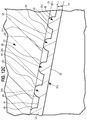
- FIGS. 8 and 9 illustrate an application of the film 30 to the waveguide body 52 of an optical waveguide 50.
- the optical waveguide 50 in this example embodiment has a light source 56 disposed in an input portion 55 having a control section 57 with a pair of control surfaces 59a, 59b.
- a coupling cavity 58 extends from the control section 57 with the waveguide body 52 extending from the coupling cavity 58.
- the control surfaces 59a, 59b may, for example, be designed to cause light developed by the light source 56 disposed in or adjacent the light coupling cavity 58 to be directed into the extended arm portions of the waveguide body 52. Light rays may travel through the waveguide body 52 due to total internal reflection.
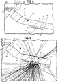
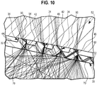
- the light rays continue to travel through the waveguide body 52 until such rays strike an index of reflection surface at a particular angle less than an angle measured with respect to a line normal to the surface point at which a light ray is incident or, equivalently, until the light rays exceed an angle measured with respect to a line tangent to the surface point at which the light ray is incident, and the light rays escape, as seen in FIGS. 9 and 10 .
- the light source 56 may develop light that is coupled into the waveguide body 52 via coupling cavity 58.
- the light source 56 may be one or more light emitting diodes (LEDs) or other alternative light source suitable to emit light to the waveguide body 52.
- the light source 56 may be a white LED or may comprise an LED module or multiple LEDs including a phosphor-coated LED either alone or in combination with a color LED, such as a green LED, etc. In those cases where a soft white illumination is to be produced, the light source may include a blue shifted yellow LED and a red LED. Different color temperatures and appearances could be produced using other LED combinations, as is known in the art.
- extraction film 30 is aligned with an extraction surface 54 of the waveguide body 52 such that the light extraction elements 34 are positioned to contact the extraction surface 54.
- the waveguide body 52 and the extraction film 30 may be made of the same material.
- both the waveguide body 52 and the embossed extraction film member 30 may be made of an acrylic material, a silicone, a polycarbonate, glass, or other suitable optically transmissive material.
- the waveguide body 52 and the extraction film 30 may be made from different optically transmissive materials.
- the extraction film 30 is shown secured to extraction surface 54 of the waveguide body 52.
- the truncated hemispherical light extraction elements 34 may be laminated to the bottom surface 60 of the waveguide body 52 to provide undercut geometries for implementing TIR extraction.
- the light extraction elements 34 are disposed between the base 32 and the bottom surface 60 of the waveguide body 52 such that reflected light from the waveguide body 52 enters the extraction member 30 through the truncated hemispherical light extraction elements 34.
- the truncated hemispherical light extraction elements 34 laminated to the bottom surface 60 of the waveguide body 52 and disposed atop the base 32 provide for illumination patterns to be developed for general illumination.
- the bottom surface 60 of the waveguide body 52 may be a generally smooth surface with the laminated embossed extraction film 30 providing for controlled extraction of light from the bottom surface 60.
- a top surface 62 opposing the bottom surface 60 of the waveguide body 52 may include additional alternatively shaped light extraction elements 64 to be disposed on the top surface.
- the additional alternative light extraction elements 64 may be formed of various patterns or configurations along the top surface 62 of the waveguide body 52 to provide a desired extraction feature.
- the top surface 62 may be textured or stepped with alternating ridges and troughs or may comprise any other structures.
- the bottom surface 60 of the waveguide body 52 may also be textured, stepped or otherwise modified from a smooth surface to provide a light extraction feature along with the extraction film 30 secured thereto.
- the extraction film 30 is shown applied to the waveguide body 52 wherein the film has an index of refraction that is the same or nearly identical to the index of refraction for the waveguide body.
- the waveguide body 52 and the extraction film 30 are made of the same material.
- light rays propagating within the waveguide body 52 may enter the extraction film 30 through an 'aperture' or interface created by bonding the flat surfaces 42 of the light extraction elements 34 to the extraction surface 54 of the waveguide body 52. Certain light rays may encounter the rounded or primary extraction surface 48 of the undercut light extraction elements 34 and reflect or refract from the curved surface 48 depending on the angle of incidence.
- Light rays may then be directed towards the base 32 and exit a bottom surface 70 of the film 30 for controlled extraction.
- the rounded surface 48 of the truncated hemispherical light extraction elements 34 provides for undercut features and extraction geometries for controlled illumination. Additionally, illumination patterns may selectively be varied based on the height of the truncated hemispherical light extraction elements of the extraction member.
- the light extraction elements 34 of the extraction film 30 disposed on the bottom surface 60 of the waveguide body 52 cause the light rays to exit the waveguide body 52 in a controlled fashion.
- the light rays that interact with the curved extraction surfaces 48 first enter the extraction film 30 through the aperture formed by the contact between the top of the light extraction element 42 and the bottom surface 60 of the waveguide.
- the aperture at the flat surface 42 of the light extraction elements 34 ensures that the light rays interacting with the curved extraction surfaces 48 do so primarily after reflecting off the top waveguide surface 62 ( FIG. 9 ). This approach provides significant benefits over known extractors having extraction surfaces that interact with light incident from both waveguide surfaces.
- Controlling the angular distribution of rays may be achieved via various optical surfaces such as the primary optic or lens of the LED 56, FIG. 9 , waveguide control 57 and the control surfaces 59, etc. Controlling the angular distribution of light within the waveguide as well as control over the direction of the light rays hitting the extraction surfaces 48 can provide additional control over the emitted illuminance distribution, luminance distribution, optical efficiency and directionality of the luminaire.
- the light reflective member 72 may be disposed above the optical waveguide 50.
- the reflector 72 may include a surface 74 that has a white or specular reflective coating or other member secured or otherwise applied thereto. Light exiting the top surface 62 of the waveguide 50 is reflected off the surface 74 and re-directed downward through the waveguide and extraction film 30 where it may provide useful illumination for the room, thereby improving efficiency.
- example extraction films 30a, 30b, 30c are shown each having corresponding light extraction elements 34a, 34b, 34c having different respective heights H2a, H2b, H2c.
- FIGS. 12A-12C illustrate the different sized gaps between the top surface 44 of the lenticular film base 32 and the bottom extraction surface 54 of the waveguide body 52.
- the extraction films and the optical waveguides may be formed from the same material have the same or near identical index of refraction in the examples of FIGS. 12A-12C .
- the gap in each example embodiment corresponds to the height H2a, H2b, H2c of the truncated hemispherical light extraction elements 34a, 34b, 34c.
- varying the length of the gap i.e., the height H2a, H2b, H2c
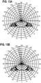
- the illuminance distributions shown in FIGS. 13A-13J correspond to the simulated distributions obtained by systematically varying the height H from 132 micrometers to 574 micrometers.
- the extraction films each have the same base height H1 and the same hexagonal array pattern of light extraction elements.
- the extraction film 30a, 30b, 30c comprised a 1.5 millimeter x 1.3 millimeter hexagonal array of light extraction elements with a 600 micrometer radius and a base height of 500 micrometers, with the extraction films each secured to a 1° tapered waveguide.
- the truncated hemispherical light extraction elements 34a had a height (H2a) of 181 micrometers which resulted in an illuminance distribution pattern corresponding to pattern seen in FIG. 13B .
- H2a height
- the truncated hemispherical light extraction elements 34b had a height (H2b) of 378 micrometers which resulted in an illuminance distribution pattern corresponding to the pattern seen in FIG. 13F .
- the truncated hemispherical light extraction elements 34c had a height (H2c) of 574 micrometers which resulted in an illuminance distribution pattern corresponding to the patterns seen in FIG. 13J .
- H2c height of 574 micrometers which resulted in an illuminance distribution pattern corresponding to the patterns seen in FIG. 13J .
- a wide range of highly controlled illuminance distributions may be achieved with the extraction film provided herein by varying the gap between the base of the extraction film and the surface of the waveguide body.
- the height(s) of the light extraction elements 34 affect the distribution of the light illumination of the waveguide 50.
- a waveguide 50 that has light extraction elements 34 disposed thereon produces an illumination distribution that varies with the height of the light extraction element (the illumination distribution shown in FIGS. 13A-13J assume that the light extraction elements 34 of the same extraction film 30 are all of substantially the same height).
- the illumination pattern of FIG. 13A is provided with an extraction film having a light extraction element height of 132 micrometers.
- the pattern of FIG. 13B is provided with a light extraction element height of 181 micrometers; FIG. 13C at a height of 230 micrometers; FIG. 13D at a height of 279 micrometers; FIG.
- FIG. 13E at a height of 328 micrometers
- FIG. 13F at a height of 378 micrometers
- FIG. 13G at a height of 427 micrometers
- FIG. 13H at a height of 476 micrometers
- FIG. 13I at a height of 525 micrometers
- FIG. 13J at a height of 574 micrometers.
- the illuminance distribution varies from a "wall-wash" distribution (i.e., a distribution having significant side-to-side illumination component) at light extractor heights of about 279 micrometers in FIG. 13D , to a nearly Lambertian distribution at light extractor heights of about 427 micrometers in FIG.
- the illumination variances are due to variations in optical coupling surface area and light extraction aperture area between flat surface 42 of the undercut light extraction elements 34 and waveguide body 52 as the cross-sectional dimensions of the light extraction elements vary with height.
- the undercut light extraction elements provide a wide range of illuminance distributions by varying the gap between the lenticular film base and the surface of the waveguide body.
Landscapes
- Physics & Mathematics (AREA)
- General Physics & Mathematics (AREA)
- Optics & Photonics (AREA)
- Engineering & Computer Science (AREA)
- Manufacturing & Machinery (AREA)
- Planar Illumination Modules (AREA)
- Optical Integrated Circuits (AREA)
Claims (13)
- Dispositif d'éclairage, comprenant :
un guide d'onde optique, comprenant :un corps de guide d'onde comprenant :un premier bras de corps de guide d'onde comprenant une première portion et une deuxième portion disposée selon un angle non nul par rapport à la première portion ;un deuxième bras de corps de guide d'onde comprenant une troisième portion et une quatrième portion disposée selon l'angle non nul par rapport à la troisième portion, dans lequel une cavité de couplage est définie entre la deuxième portion et la quatrième portion ; etun premier film disposé sur une première surface de la première portion du premier bras de corps de guide d'onde, dans lequel le premier film comprend une première base et une première pluralité d'éléments d'extraction de lumière creusés disposés entre la première base et la première surface, et dans lequel chacun d'au moins certains de la première pluralité d'éléments d'extraction de lumière creusés comprend une première forme incurvée en coupe transversale ;un deuxième film disposé sur une troisième surface de la troisième portion du deuxième bras de corps de guide d'onde, dans lequel le deuxième film comprend une deuxième base et une deuxième pluralité d'éléments d'extraction de lumière creusés disposés entre la deuxième base et la troisième surface, et dans lequel chacun d'au moins certains de la deuxième pluralité d'éléments d'extraction de lumière creusés comprend une deuxième forme incurvée en coupe transversale ; etune source de lumière disposée de manière adjacente à la deuxième portion et à la quatrième portion de telle sorte que de la lumière provenant de la source de lumière est totalement réfléchie de manière interne à travers la deuxième portion et la quatrième portion dans la première portion et la troisième portion, respectivement, et la lumière est extraite via la première pluralité d'éléments d'extraction de lumière creusés et la deuxième pluralité d'éléments d'extraction de lumière creusés, respectivement. - Dispositif d'éclairage selon la revendication 1, comprenant en outre une troisième pluralité d'éléments d'extraction de lumière creusés disposés sur une deuxième surface de la première portion opposée à la première surface et une quatrième pluralité d'éléments d'extraction de lumière creusés disposés sur une quatrième surface de la troisième portion opposée à la troisième surface.
- Dispositif d'éclairage selon l'une quelconque des revendications précédentes, dans lequel la première pluralité et la deuxième pluralité d'éléments d'extraction de lumière creusés sont disposés en ensembles hexagonaux.
- Dispositif d'éclairage selon l'une quelconque des revendications précédentes, dans lequel la totalité des première et deuxième pluralités d'éléments d'extraction de lumière comprennent sensiblement la même hauteur.
- Dispositif d'éclairage selon l'une quelconque des revendications précédentes, dans lequel chacune des première et deuxième bases comprend une épaisseur constante.
- Dispositif d'éclairage selon les revendications 4 et 5 en combinaison, dans lequel chacun des première et deuxième pluralités d'éléments d'extraction de lumière creusés comprend une forme tronquée et chacun des première et deuxième pluralités d'éléments d'extraction de lumière creusés a sensiblement la même hauteur dans une plage d'environ 100 micromètres à environ 590 micromètres et l'épaisseur de chacune des première et deuxième bases est d'environ 500 micromètres.
- Dispositif d'éclairage selon l'une quelconque des revendications précédentes, comprenant en outre un premier réflecteur disposé de manière adjacente à une deuxième surface de la première portion du premier bras de corps de guide d'onde opposée à la première surface et un deuxième réflecteur disposé de manière adjacente à une quatrième surface de la troisième portion du deuxième bras de corps de guide d'onde opposée à la troisième surface.
- Dispositif d'éclairage selon l'une quelconque des revendications précédentes, dans lequel les première et deuxième formes incurvées en coupe transversale sont hémisphériques.
- Dispositif d'éclairage selon l'une quelconque des revendications précédentes, dans lequel chacun des premiers et deuxièmes éléments d'extraction de lumière creusés comprend une première dimension en coupe transversale proximale aux première et deuxième bases, respectivement, et une deuxième dimension en coupe transversale plus petite que la première dimension en coupe transversale distale des première et deuxième bases, respectivement.
- Dispositif d'éclairage selon l'une quelconque des revendications précédentes, dans lequel les bras de corps de guide d'onde et les premier et deuxième films sont composés du même matériau.
- Dispositif d'éclairage selon l'une quelconque des revendications 1 à 9, dans lequel les premier et deuxième bras de corps de guide d'onde et les premier et deuxième films sont composés de matériaux différents.
- Dispositif d'éclairage selon l'une quelconque des revendications précédentes, dans lequel les première et deuxième pluralités d'éléments d'extraction de lumière creusés comprennent chacun une forme en coupe transversale tronquée.
- Dispositif d'éclairage selon la revendication 11, dans lequel la forme en coupe transversale tronquée est hémisphérique.
Applications Claiming Priority (2)
| Application Number | Priority Date | Filing Date | Title |
|---|---|---|---|
| US201461925589P | 2014-01-09 | 2014-01-09 | |
| US14/471,991 US9651740B2 (en) | 2014-01-09 | 2014-08-28 | Extraction film for optical waveguide and method of producing same |
Publications (2)
| Publication Number | Publication Date |
|---|---|
| EP2894396A1 EP2894396A1 (fr) | 2015-07-15 |
| EP2894396B1 true EP2894396B1 (fr) | 2018-10-24 |
Family
ID=51868864
Family Applications (1)
| Application Number | Title | Priority Date | Filing Date |
|---|---|---|---|
| EP14192325.0A Active EP2894396B1 (fr) | 2014-01-09 | 2014-11-07 | Film d'extraction pour guide d'ondes et son procédé de production |
Country Status (3)
| Country | Link |
|---|---|
| US (1) | US9651740B2 (fr) |
| EP (1) | EP2894396B1 (fr) |
| CN (1) | CN104777554B (fr) |
Families Citing this family (15)
| Publication number | Priority date | Publication date | Assignee | Title |
|---|---|---|---|---|
| US10436969B2 (en) | 2013-01-30 | 2019-10-08 | Ideal Industries Lighting Llc | Optical waveguide and luminaire incorporating same |
| US9366396B2 (en) | 2013-01-30 | 2016-06-14 | Cree, Inc. | Optical waveguide and lamp including same |
| US9625638B2 (en) | 2013-03-15 | 2017-04-18 | Cree, Inc. | Optical waveguide body |
| US9798072B2 (en) * | 2013-03-15 | 2017-10-24 | Cree, Inc. | Optical element and method of forming an optical element |
| US9366799B2 (en) | 2013-03-15 | 2016-06-14 | Cree, Inc. | Optical waveguide bodies and luminaires utilizing same |
| US10209429B2 (en) | 2013-03-15 | 2019-02-19 | Cree, Inc. | Luminaire with selectable luminous intensity pattern |
| US9651740B2 (en) | 2014-01-09 | 2017-05-16 | Cree, Inc. | Extraction film for optical waveguide and method of producing same |
| KR102244427B1 (ko) * | 2014-06-02 | 2021-04-27 | 엘지이노텍 주식회사 | 조명 장치 |
| CN104121516B (zh) * | 2014-07-11 | 2016-08-17 | 京东方科技集团股份有限公司 | 用于台灯的灯头及台灯 |
| US11719882B2 (en) | 2016-05-06 | 2023-08-08 | Ideal Industries Lighting Llc | Waveguide-based light sources with dynamic beam shaping |
| US10416377B2 (en) | 2016-05-06 | 2019-09-17 | Cree, Inc. | Luminaire with controllable light emission |
| DE102016118884A1 (de) * | 2016-10-05 | 2018-04-05 | Temicon Gmbh | Lichtumlenkvorrichtung, Beleuchtungseinrichtung und Verwendung |
| US10364948B2 (en) * | 2017-05-10 | 2019-07-30 | Ideal Industries Lighting Llc | Optical waveguides and luminaires having a waveguide with extraction features and reflective material having openings disposed thereon |
| GB2566711B (en) * | 2017-09-22 | 2020-08-19 | Visteon Global Tech Inc | A backlight panel for providing area backlighting of a panel display device |
| AU2019239786A1 (en) * | 2018-03-19 | 2020-10-22 | Terra Firma Innovations Inc. | Photovoltaic microcell array with multi-stage concentrating optics |
Citations (1)
| Publication number | Priority date | Publication date | Assignee | Title |
|---|---|---|---|---|
| US7001060B1 (en) * | 1999-08-11 | 2006-02-21 | Semiconductor Energy Laboratory Co., Ltd. | Front light having a plurality of prism-shaped lenses |
Family Cites Families (205)
| Publication number | Priority date | Publication date | Assignee | Title |
|---|---|---|---|---|
| US615108A (en) | 1898-11-29 | de segundo | ||
| US766515A (en) | 1904-01-26 | 1904-08-02 | Elmer C Northrup | Elevator. |
| US2047137A (en) | 1932-06-07 | 1936-07-07 | Budd Wheel Co | Artillery wheel structure |
| US2014268A (en) | 1933-03-02 | 1935-09-10 | Tenney Vernon | Coaster |
| US2992587A (en) | 1958-04-11 | 1961-07-18 | American Optical Corp | Fiber optical devices |
| US3532871A (en) | 1968-05-20 | 1970-10-06 | Ford Motor Co | Combination running light-reflector |
| JPS6134583A (ja) | 1984-07-26 | 1986-02-18 | シャープ株式会社 | 照明装置 |
| USD298861S (en) | 1986-02-03 | 1988-12-06 | Manville Corporation | Area light |
| US5005108A (en) | 1989-02-10 | 1991-04-02 | Lumitex, Inc. | Thin panel illuminator |
| US5309544A (en) | 1992-03-31 | 1994-05-03 | Minnesota Mining And Manufacturing Company | Light pipe having optimized cross-section |
| US5897201A (en) | 1993-01-21 | 1999-04-27 | Simon; Jerome H. | Architectural lighting distributed from contained radially collimated light |
| US5481385A (en) | 1993-07-01 | 1996-01-02 | Alliedsignal Inc. | Direct view display device with array of tapered waveguide on viewer side |
| US5521725A (en) | 1993-11-05 | 1996-05-28 | Alliedsignal Inc. | Illumination system employing an array of microprisms |
| US5555329A (en) | 1993-11-05 | 1996-09-10 | Alliesignal Inc. | Light directing optical structure |
| US5428468A (en) | 1993-11-05 | 1995-06-27 | Alliedsignal Inc. | Illumination system employing an array of microprisms |
| US5396350A (en) * | 1993-11-05 | 1995-03-07 | Alliedsignal Inc. | Backlighting apparatus employing an array of microprisms |
| US5462700A (en) | 1993-11-08 | 1995-10-31 | Alliedsignal Inc. | Process for making an array of tapered photopolymerized waveguides |
| US5598281A (en) | 1993-11-19 | 1997-01-28 | Alliedsignal Inc. | Backlight assembly for improved illumination employing tapered optical elements |
| US5506924A (en) | 1994-08-23 | 1996-04-09 | Inoue Denki Co., Inc. | Light guiding plate |
| US5521726A (en) | 1994-08-26 | 1996-05-28 | Alliedsignal Inc. | Polarizer with an array of tapered waveguides |
| US5657408A (en) | 1994-12-23 | 1997-08-12 | Alliedsignal Inc. | Optical device comprising a plurality of units having at least two geometrically-differentiated tapered optical waveguides therein |
| KR100398940B1 (ko) * | 1995-03-03 | 2003-12-31 | 미네소타 마이닝 앤드 매뉴팩춰링 캄파니 | 다양한높이의구조화면을갖는광지향성필름과이러한필름으로구성된물품 |
| US5613751A (en) | 1995-06-27 | 1997-03-25 | Lumitex, Inc. | Light emitting panel assemblies |
| US6712481B2 (en) | 1995-06-27 | 2004-03-30 | Solid State Opto Limited | Light emitting panel assemblies |
| US5624202A (en) | 1995-10-19 | 1997-04-29 | Ledalite Architectural Products, Inc. | Integral joint and mounting assembly for suspended linear structures |
| US5839823A (en) | 1996-03-26 | 1998-11-24 | Alliedsignal Inc. | Back-coupled illumination system with light recycling |
| KR100240288B1 (ko) | 1997-01-24 | 2000-01-15 | 박강정 | 장식용 발광장치 |
| US5812714A (en) | 1997-01-30 | 1998-09-22 | Cooper Industries, Inc. | Optical waveguide elements for a distributed lighting system |
| US6259854B1 (en) | 1997-05-29 | 2001-07-10 | Kuraray Co., Ltd. | Lightguide |
| US5949933A (en) | 1998-03-03 | 1999-09-07 | Alliedsignal Inc. | Lenticular illumination system |
| JP4159059B2 (ja) | 1998-06-05 | 2008-10-01 | シチズン電子株式会社 | 面状光源ユニット |
| US6752505B2 (en) | 1999-02-23 | 2004-06-22 | Solid State Opto Limited | Light redirecting films and film systems |
| WO2001002772A1 (fr) | 1999-07-01 | 2001-01-11 | 3M Innovative Properties Company | Ensemble d'affichage dote d'un guide optique frontal |
| US6971758B2 (en) | 2001-03-16 | 2005-12-06 | Toyoda Gosei Co., Ltd. | Illumination device |
| US6985163B2 (en) | 2001-08-14 | 2006-01-10 | Sarnoff Corporation | Color display device |
| JP4122161B2 (ja) | 2002-02-04 | 2008-07-23 | 日本電産コパル株式会社 | 面発光装置 |
| FR2836208B1 (fr) | 2002-02-21 | 2004-09-03 | Valeo Vision | Feu de signalisation comportant une piece optique realisant une fonction de signalisation de maniere autonome |
| US6724529B2 (en) | 2002-04-17 | 2004-04-20 | Howard Sinkoff | Reflection-type projection screens |
| US7010212B2 (en) | 2002-05-28 | 2006-03-07 | 3M Innovative Properties Company | Multifunctional optical assembly |
| JP4162935B2 (ja) | 2002-07-04 | 2008-10-08 | 株式会社小糸製作所 | 車両用灯具 |
| US6948832B2 (en) | 2002-09-10 | 2005-09-27 | Honeywell International, Inc. | Luminaire device |
| JP4436105B2 (ja) | 2002-11-29 | 2010-03-24 | 富士通株式会社 | リフレクタ及び照明装置及び導光板及び表示装置 |
| JP4222036B2 (ja) | 2003-01-23 | 2009-02-12 | 日亜化学工業株式会社 | 面発光装置用導光板と面発光装置 |
| US6795611B2 (en) | 2003-01-29 | 2004-09-21 | Institut National D'optique | Light coupling between a light source and an optical waveguide |
| US7008097B1 (en) | 2003-02-25 | 2006-03-07 | Ilight Technologies, Inc. | Illumination device for simulating neon or fluorescent lighting including a waveguide and a scattering cap |
| US7182480B2 (en) | 2003-03-05 | 2007-02-27 | Tir Systems Ltd. | System and method for manipulating illumination created by an array of light emitting devices |
| EP1660918B1 (fr) | 2003-07-29 | 2017-03-15 | Light Engine Limited | Luminaires a emission de lumiere peripherique et elements de lentilles formes par des profils de balayage a axe transversal |
| JP2005158362A (ja) | 2003-11-21 | 2005-06-16 | Stanley Electric Co Ltd | 車両用灯具 |
| JP4020397B2 (ja) | 2004-06-14 | 2007-12-12 | 惠次 飯村 | 点光源を用いた面光源 |
| US7730967B2 (en) | 2004-06-22 | 2010-06-08 | Baker Hughes Incorporated | Drilling wellbores with optimal physical drill string conditions |
| US7083313B2 (en) | 2004-06-28 | 2006-08-01 | Whelen Engineering Company, Inc. | Side-emitting collimator |
| EP1781470B1 (fr) | 2004-07-15 | 2013-11-27 | Rodger T. Cosgrove | Procede de production d'enveloppe d'expedition sur demande |
| US20060018126A1 (en) | 2004-07-22 | 2006-01-26 | Kueun Choi | Edge-lit lighted panel for bulletin boards |
| US8283354B2 (en) | 2004-09-02 | 2012-10-09 | Vertex Pharmaceuticals Incorporated | Quinazolines useful as modulators of ion channels |
| US8033706B1 (en) | 2004-09-09 | 2011-10-11 | Fusion Optix, Inc. | Lightguide comprising a low refractive index region |
| US7775700B2 (en) | 2004-10-01 | 2010-08-17 | Rohm And Haas Electronics Materials Llc | Turning film using array of roof prism structures |
| US8541795B2 (en) | 2004-10-12 | 2013-09-24 | Cree, Inc. | Side-emitting optical coupling device |
| JP2006131444A (ja) | 2004-11-04 | 2006-05-25 | Shin Etsu Chem Co Ltd | 光学部品用光ファイバ母材およびその製造方法、並びに光ファイバ |
| US8430548B1 (en) | 2004-11-17 | 2013-04-30 | Fusion Optix, Inc. | Enhanced light fixture with volumetric light scattering |
| DE102004063574A1 (de) | 2004-12-30 | 2006-07-13 | Osram Opto Semiconductors Gmbh | Leuchtvorrichtung mit mehreren Halbleiterlichtquellen |
| US7416309B2 (en) * | 2004-12-30 | 2008-08-26 | 3M Innovative Properties Company | Optical film having a surface with rounded structures |
| JP2006221922A (ja) | 2005-02-09 | 2006-08-24 | Mitsubishi Rayon Co Ltd | Led面状光源装置 |
| KR100631904B1 (ko) | 2005-02-18 | 2006-10-11 | 삼성전기주식회사 | 도광 기능을 갖는 직하형 백라이트 장치 |
| WO2006093087A1 (fr) | 2005-02-28 | 2006-09-08 | Kuraray Co., Ltd. | Film de photodiffusion, élément de source lumineuse plan utilisant ledit film et dispositif d’affichage à cristaux liquides |
| JP4282625B2 (ja) | 2005-03-10 | 2009-06-24 | 株式会社東芝 | 半導体装置及びその製造方法 |
| JP2007123130A (ja) | 2005-10-28 | 2007-05-17 | Citizen Electronics Co Ltd | バックライトユニット及びそれを備えた表示機器 |
| US7322733B2 (en) | 2005-11-09 | 2008-01-29 | Applied Research Laboratories, National Center For High-Performance Computing | Light guide plate having micro-reflectors |
| US7477828B2 (en) | 2006-01-06 | 2009-01-13 | Lockheed Martin Corporation | Optical waveguide |
| WO2007087710A1 (fr) | 2006-02-01 | 2007-08-09 | Tir Technology Lp | Systeme d'eclairage pour créer une surface eclairée |
| US7593615B2 (en) | 2006-02-10 | 2009-09-22 | Rpc Photonics, Inc. | Optical devices for guiding illumination |
| DE102006009325A1 (de) | 2006-03-01 | 2007-09-06 | Karl Jungbecker Gmbh & Co | Optisches System zur Richtung des Lichtes durch eine Mikrokegelstruktur |
| DE102006011296A1 (de) | 2006-03-11 | 2007-09-13 | Karl Jungbecker Gmbh & Co | Optisches System zur Richtung des Lichtes beliebiger Leuchtmittel |
| US20070223252A1 (en) * | 2006-03-24 | 2007-09-27 | Junwon Lee | Illumination apparatus and film |
| US7452120B2 (en) | 2006-03-24 | 2008-11-18 | Rohm And Haas Denmark Finance A/S | Illumination apparatus and film |
| US9335006B2 (en) | 2006-04-18 | 2016-05-10 | Cree, Inc. | Saturated yellow phosphor converted LED and blue converted red LED |
| CN101448632B (zh) | 2006-05-18 | 2012-12-12 | 3M创新有限公司 | 用于制备具有提取结构的光导的方法以及由此方法生产的光导 |
| TWM304683U (en) * | 2006-06-02 | 2007-01-11 | Coretronic Corp | Edge-type backlight module |
| US7703945B2 (en) | 2006-06-27 | 2010-04-27 | Cree, Inc. | Efficient emitting LED package and method for efficiently emitting light |
| US8113687B2 (en) | 2006-06-29 | 2012-02-14 | Cree, Inc. | Modular LED lighting fixture |
| US7771087B2 (en) | 2006-09-30 | 2010-08-10 | Ruud Lighting, Inc. | LED light fixture with uninterruptible power supply |
| WO2008045311A2 (fr) * | 2006-10-06 | 2008-04-17 | Qualcomm Mems Technologies, Inc. | Dispositif d'éclairage intégrant un coupleur de lumière |
| TW200835887A (en) | 2006-10-16 | 2008-09-01 | Koninkl Philips Electronics Nv | Luminaire with LEDs |
| US20080094853A1 (en) | 2006-10-20 | 2008-04-24 | Pixtronix, Inc. | Light guides and backlight systems incorporating light redirectors at varying densities |
| US7455416B2 (en) | 2006-11-17 | 2008-11-25 | Ichia Technologies, Inc. | Light guide structure and keypad having the same |
| GB2443849A (en) | 2006-11-20 | 2008-05-21 | Sharp Kk | Backlight and display |
| US20080130908A1 (en) | 2006-12-05 | 2008-06-05 | Searete Llc, A Limited Liability Corporation Of The State Of Delaware | Selective audio/sound aspects |
| TW200825529A (en) | 2006-12-06 | 2008-06-16 | Chi Lin Technology Co Ltd | Light mixer and backlight module having it |
| TWI356238B (en) | 2007-02-12 | 2012-01-11 | Chimei Innolux Corp | Backlight module and liquid crystal display using |
| US8511868B2 (en) | 2007-04-02 | 2013-08-20 | Cree, Inc. | Remote ballast housing with airflow channel |
| CN103822172B (zh) | 2007-04-05 | 2017-07-28 | 飞利浦灯具控股公司 | 光束成形器 |
| EP2145130B1 (fr) | 2007-04-10 | 2014-12-17 | Ledalite Architectural Products, Inc. | Appareil de commande lumineux présentant une répartition de l'intensité lumineuse en éventail dans les hémisphères supérieur et inférieur |
| WO2008126023A2 (fr) | 2007-04-16 | 2008-10-23 | Koninklijke Philips Electronics N.V. | Structure optique |
| CN101295038A (zh) | 2007-04-27 | 2008-10-29 | 鸿富锦精密工业(深圳)有限公司 | 背光模组及其光学板 |
| CN101295044B (zh) | 2007-04-27 | 2011-06-29 | 鸿富锦精密工业(深圳)有限公司 | 背光模组及其光学板 |
| CN101295045A (zh) | 2007-04-27 | 2008-10-29 | 鸿富锦精密工业(深圳)有限公司 | 背光模组及其光学板 |
| CN101303428A (zh) | 2007-05-08 | 2008-11-12 | 鸿富锦精密工业(深圳)有限公司 | 背光模组及其光学板 |
| US8277106B2 (en) | 2007-05-10 | 2012-10-02 | Koninklijke Philips Electronics N.V. | Lighting device |
| US20080285274A1 (en) | 2007-05-17 | 2008-11-20 | Hae-Ryong Jung Jung | Panel light source for back-lit signs |
| CN101334554B (zh) | 2007-06-28 | 2011-07-27 | 鸿富锦精密工业(深圳)有限公司 | 背光模组及其光学板 |
| CN101344610B (zh) | 2007-07-12 | 2011-06-29 | 鸿富锦精密工业(深圳)有限公司 | 背光模组及其光学板 |
| CN101354449B (zh) | 2007-07-23 | 2011-09-28 | 鸿富锦精密工业(深圳)有限公司 | 背光模组及其光学板 |
| CN101408640A (zh) | 2007-10-09 | 2009-04-15 | 富士迈半导体精密工业(上海)有限公司 | 光源模组 |
| CN101158781A (zh) * | 2007-11-12 | 2008-04-09 | 杨忠义 | 双面液晶显示屏 |
| US7791683B2 (en) | 2007-11-19 | 2010-09-07 | Honeywell International Inc. | Backlight systems for liquid crystal displays |
| US7845826B2 (en) | 2008-01-15 | 2010-12-07 | Skc Haas Display Films Co., Ltd. | Multilayered integrated backlight illumination assembly |
| TWI352222B (en) * | 2008-01-16 | 2011-11-11 | Coretronic Corp | Light-collimating film |
| EP2247978A4 (fr) | 2008-01-30 | 2012-12-26 | Qualcomm Mems Technologies Inc | Système d éclairage mince |
| JP2009218076A (ja) | 2008-03-10 | 2009-09-24 | Koito Mfg Co Ltd | 車両用灯具 |
| US8079739B2 (en) | 2008-04-01 | 2011-12-20 | Cooper James M | Interlocking system for hanging decorative lights and fixtures |
| US8690384B2 (en) | 2008-06-06 | 2014-04-08 | Relume Technologies, Inc. | Integral heat sink and housing light emitting diode assembly |
| US20090310367A1 (en) | 2008-06-17 | 2009-12-17 | Shih-Yuan Kuo | Composite light guide structure |
| CN101608768A (zh) | 2008-06-18 | 2009-12-23 | 富准精密工业(深圳)有限公司 | 发光二极管灯具 |
| US8292480B2 (en) | 2008-07-10 | 2012-10-23 | Koito Manufacturing Co., Ltd. | Lamp including main reflector, sub-reflector and LED assembly |
| US8301002B2 (en) | 2008-07-10 | 2012-10-30 | Oree, Inc. | Slim waveguide coupling apparatus and method |
| TW201007647A (en) * | 2008-07-10 | 2010-02-16 | 3M Innovative Properties Co | Retroreflective articles and devices having viscoelastic lightguide |
| US8057056B2 (en) | 2008-08-09 | 2011-11-15 | Tsinghua University | Light guide plates and backlight module |
| KR101286095B1 (ko) | 2008-09-11 | 2013-07-15 | 엘지디스플레이 주식회사 | 액정표시장치용 일체형 멀티집광시트 |
| JP2010083692A (ja) | 2008-09-30 | 2010-04-15 | Tdk Corp | NiMnZn系フェライト |
| TWI407043B (zh) | 2008-11-04 | 2013-09-01 | Advanced Optoelectronic Tech | 發光二極體光源模組及其光學引擎 |
| JP2010123309A (ja) | 2008-11-18 | 2010-06-03 | Nittoh Kogaku Kk | 光学素子および発光装置 |
| CN101750665B (zh) | 2008-12-12 | 2011-09-28 | 清华大学 | 导光板以及使用该导光板的背光模组 |
| US8376582B2 (en) | 2009-03-18 | 2013-02-19 | Koninklijke Philips Electronics N.V. | LED luminaire |
| US8212263B2 (en) | 2009-04-03 | 2012-07-03 | Koninklijke Philips Electronics N.V. | Backlight including semiconductior light emitting devices |
| US8948564B1 (en) * | 2009-04-16 | 2015-02-03 | Fusion Uptix, Inc. | Spline lamp with opposing light source orientation |
| US8953926B1 (en) * | 2009-04-16 | 2015-02-10 | Fusion Optix, Inc. | Spline optic and lighting device |
| US8750671B1 (en) * | 2009-04-16 | 2014-06-10 | Fusion Optix, Inc | Light bulb with omnidirectional output |
| US8761565B1 (en) * | 2009-04-16 | 2014-06-24 | Fusion Optix, Inc. | Arcuate lightguide and light emitting device comprising the same |
| CN102395915B (zh) | 2009-04-22 | 2014-04-16 | 株式会社藤仓 | 显示装置以及采光窗 |
| US8783898B2 (en) | 2009-05-01 | 2014-07-22 | Abl Ip Holding Llc | Light emitting devices and applications thereof |
| US8921876B2 (en) | 2009-06-02 | 2014-12-30 | Cree, Inc. | Lighting devices with discrete lumiphor-bearing regions within or on a surface of remote elements |
| NO332115B1 (no) | 2009-07-07 | 2012-06-25 | Kongsberg Seatex As | Styringsinnretning for posisjonering av instrumentert tauet kabel i vann |
| WO2011004306A1 (fr) | 2009-07-10 | 2011-01-13 | Koninklijke Philips Electronics N.V. | Module d'éclairage de forme libre |
| CN102472864B (zh) | 2009-07-20 | 2016-06-15 | 3M创新有限公司 | 具有多个反射器的中空光导 |
| US8449128B2 (en) | 2009-08-20 | 2013-05-28 | Illumitex, Inc. | System and method for a lens and phosphor layer |
| CN201487753U (zh) | 2009-08-28 | 2010-05-26 | 睿鸿光电科技(福建)有限公司 | Led吸顶灯 |
| US9075179B2 (en) | 2009-09-14 | 2015-07-07 | Unipixel Displays, Inc. | Light-extraction graphics film |
| US8310158B2 (en) | 2009-09-23 | 2012-11-13 | Ecofit Lighting, LLC | LED light engine apparatus |
| EP3258167A3 (fr) * | 2009-12-08 | 2018-04-18 | 3M Innovative Properties Co. | Constructions optique comprenant un guide de lumière et des films à faible indice de réfraction |
| CA2729481A1 (fr) | 2010-01-30 | 2011-07-30 | Koninklijke Philips Electronics N.V. | Systeme de commande de l'eclairage d'une pluralite de luminaires |
| TWI454760B (zh) | 2010-02-06 | 2014-10-01 | Hon Hai Prec Ind Co Ltd | 背光模組及其導光板 |
| US9097824B2 (en) | 2010-03-18 | 2015-08-04 | Koninklijke Philips N.V. | Light mixing module, and a luminaire comprising such a light mixing module |
| US9012938B2 (en) | 2010-04-09 | 2015-04-21 | Cree, Inc. | High reflective substrate of light emitting devices with improved light output |
| TWI412804B (zh) | 2010-04-14 | 2013-10-21 | Entire Technology Co Ltd | 多層導光裝置 |
| WO2011130715A2 (fr) * | 2010-04-16 | 2011-10-20 | Flex Lighting Ii, Llc | Dispositif d'éclairage comprenant un guide de lumière basé sur un film |
| JP5518559B2 (ja) | 2010-04-22 | 2014-06-11 | スタンレー電気株式会社 | 灯具ユニット |
| US8482186B2 (en) | 2010-05-03 | 2013-07-09 | Young Lighting Technology Inc. | Lighting device |
| US8807799B2 (en) | 2010-06-11 | 2014-08-19 | Intematix Corporation | LED-based lamps |
| KR101372084B1 (ko) * | 2010-06-29 | 2014-03-07 | 쿨레지 라이팅 인크. | 항복형 기판을 갖는 전자 장치 |
| TW201202623A (en) | 2010-07-15 | 2012-01-16 | Qisda Corp | Illumination apparatus |
| CN101922633A (zh) | 2010-07-22 | 2010-12-22 | 鸿富锦精密工业(深圳)有限公司 | Led照明装置 |
| US8814391B2 (en) * | 2010-09-20 | 2014-08-26 | Luxingtek, Ltd. | Light guiding structure |
| US9075172B2 (en) | 2010-09-20 | 2015-07-07 | Luxingtek, Ltd. | Light converting optical structure and lighting device utilizing the same |
| US8702292B2 (en) | 2010-09-22 | 2014-04-22 | Terralux, Inc. | Linear illumination devices having light guides and LED-based illumination modules |
| US9494293B2 (en) | 2010-12-06 | 2016-11-15 | Cree, Inc. | Troffer-style optical assembly |
| JP5641332B2 (ja) | 2011-01-24 | 2014-12-17 | スタンレー電気株式会社 | 灯具 |
| US9645304B2 (en) * | 2011-03-09 | 2017-05-09 | Flex Lighting Ii Llc | Directional front illuminating device comprising a film based lightguide with high optical clarity in the light emitting region |
| KR101793275B1 (ko) | 2011-03-24 | 2017-11-03 | 삼성디스플레이 주식회사 | 백라이트 유닛 및 백라이트 유닛을 포함하는 표시장치 |
| US20120300456A1 (en) | 2011-05-26 | 2012-11-29 | Phillips Iii William E | Reflectors optimized for led lighting fixture |
| US8696173B2 (en) | 2011-06-08 | 2014-04-15 | GE Lighting Solutions, LLC | Low profile lamp using TIR lens |
| US8876325B2 (en) | 2011-07-01 | 2014-11-04 | Cree, Inc. | Reverse total internal reflection features in linear profile for lighting applications |
| US8744222B2 (en) | 2011-07-27 | 2014-06-03 | National Applied Research Laboratories | Practical silicon photonic multi-function integrated-optic chip for fiber sensor applications |
| US9081125B2 (en) | 2011-08-08 | 2015-07-14 | Quarkstar Llc | Illumination devices including multiple light emitting elements |
| WO2013023008A1 (fr) | 2011-08-08 | 2013-02-14 | Quarkstar Llc | Dispositifs d'éclairage comprenant de multiples éléments d'émission de lumière |
| JP5883596B2 (ja) | 2011-08-25 | 2016-03-15 | 林テレンプ株式会社 | 面照明装置 |
| CN202253389U (zh) * | 2011-08-30 | 2012-05-30 | 深圳安嵘光电产品有限公司 | 一种拼图式立体导光板和照明灯具 |
| US9234649B2 (en) | 2011-11-01 | 2016-01-12 | Lsi Industries, Inc. | Luminaires and lighting structures |
| US20130107527A1 (en) | 2011-11-01 | 2013-05-02 | Lsi Industries, Inc. | Luminaires and lighting structures |
| US20130107528A1 (en) | 2011-11-01 | 2013-05-02 | Lsi Industries, Inc. | Luminaires and lighting structures |
| US8564004B2 (en) | 2011-11-29 | 2013-10-22 | Cree, Inc. | Complex primary optics with intermediate elements |
| US8975825B2 (en) | 2012-05-08 | 2015-03-10 | Cree, Inc. | Light emitting diode driver with isolated control circuits |
| US20130317784A1 (en) | 2012-05-22 | 2013-11-28 | Jiandong Huang | Method for the Design of Uniform Waveguide Light Extraction |
| US9818919B2 (en) | 2012-06-11 | 2017-11-14 | Cree, Inc. | LED package with multiple element light source and encapsulant having planar surfaces |
| US8975827B2 (en) | 2012-07-01 | 2015-03-10 | Cree, Inc. | Lighting fixture for distributed control |
| EP3462080A1 (fr) | 2012-09-13 | 2019-04-03 | Quarkstar LLC | Systèmes d'éclairage fournissant un éclairage direct et indirect |
| US9690029B2 (en) | 2013-01-30 | 2017-06-27 | Cree, Inc. | Optical waveguides and luminaires incorporating same |
| US9625638B2 (en) | 2013-03-15 | 2017-04-18 | Cree, Inc. | Optical waveguide body |
| US9869432B2 (en) | 2013-01-30 | 2018-01-16 | Cree, Inc. | Luminaires using waveguide bodies and optical elements |
| US9291320B2 (en) | 2013-01-30 | 2016-03-22 | Cree, Inc. | Consolidated troffer |
| US9442243B2 (en) | 2013-01-30 | 2016-09-13 | Cree, Inc. | Waveguide bodies including redirection features and methods of producing same |
| WO2014120945A1 (fr) | 2013-01-30 | 2014-08-07 | Cree, Inc. | Guide d'ondes optique et lampe l'utilisant |
| US10234616B2 (en) | 2013-01-30 | 2019-03-19 | Cree, Inc. | Simplified low profile module with light guide for pendant, surface mount, wall mount and stand alone luminaires |
| US10436969B2 (en) | 2013-01-30 | 2019-10-08 | Ideal Industries Lighting Llc | Optical waveguide and luminaire incorporating same |
| US9411086B2 (en) | 2013-01-30 | 2016-08-09 | Cree, Inc. | Optical waveguide assembly and light engine including same |
| US10422944B2 (en) | 2013-01-30 | 2019-09-24 | Ideal Industries Lighting Llc | Multi-stage optical waveguide for a luminaire |
| US9366396B2 (en) | 2013-01-30 | 2016-06-14 | Cree, Inc. | Optical waveguide and lamp including same |
| US20140268879A1 (en) | 2013-03-14 | 2014-09-18 | Panasonic Corporation | Transparent waveguide diffuser for lighting and methods of manufacturing transparent waveguide diffuser |
| USD695431S1 (en) | 2013-03-15 | 2013-12-10 | Cree, Inc. | Lamp |
| US10209429B2 (en) | 2013-03-15 | 2019-02-19 | Cree, Inc. | Luminaire with selectable luminous intensity pattern |
| US9513424B2 (en) | 2013-03-15 | 2016-12-06 | Cree, Inc. | Optical components for luminaire |
| US10436970B2 (en) | 2013-03-15 | 2019-10-08 | Ideal Industries Lighting Llc | Shaped optical waveguide bodies |
| US20150177439A1 (en) | 2013-03-15 | 2015-06-25 | Cree, Inc. | Optical Waveguide Bodies and Luminaires Utilizing Same |
| US9366799B2 (en) | 2013-03-15 | 2016-06-14 | Cree, Inc. | Optical waveguide bodies and luminaires utilizing same |
| US20150049511A1 (en) | 2013-03-15 | 2015-02-19 | Cree, Inc. | Waveguide Having Unidirectional Illuminance |
| US10502899B2 (en) | 2013-03-15 | 2019-12-10 | Ideal Industries Lighting Llc | Outdoor and/or enclosed structure LED luminaire |
| US9952372B2 (en) | 2013-03-15 | 2018-04-24 | Cree, Inc. | Luminaire utilizing waveguide |
| USD702377S1 (en) | 2013-03-15 | 2014-04-08 | Cree, Inc. | Portion of a lamp |
| EP2972532B1 (fr) | 2013-03-15 | 2021-05-05 | Ideal Industries Lighting Llc | Corps de guide d'ondes optiques |
| US9645303B2 (en) | 2013-03-15 | 2017-05-09 | Cree, Inc. | Luminaires utilizing edge coupling |
| US9581750B2 (en) | 2013-03-15 | 2017-02-28 | Cree, Inc. | Outdoor and/or enclosed structure LED luminaire |
| US10379278B2 (en) | 2013-03-15 | 2019-08-13 | Ideal Industries Lighting Llc | Outdoor and/or enclosed structure LED luminaire outdoor and/or enclosed structure LED luminaire having outward illumination |
| US10400984B2 (en) | 2013-03-15 | 2019-09-03 | Cree, Inc. | LED light fixture and unitary optic member therefor |
| TW201441683A (zh) | 2013-04-26 | 2014-11-01 | Hon Hai Prec Ind Co Ltd | 光學元件以及應用該光學元件的背光模組 |
| US9046225B2 (en) | 2013-08-16 | 2015-06-02 | General Electric Company | Lighting system with improved illumination distribution |
| US9651740B2 (en) | 2014-01-09 | 2017-05-16 | Cree, Inc. | Extraction film for optical waveguide and method of producing same |
| US9464778B2 (en) | 2014-01-21 | 2016-10-11 | Cree, Inc. | Lighting device utilizing a double fresnel lens |
-
2014
- 2014-08-28 US US14/471,991 patent/US9651740B2/en active Active
- 2014-11-07 EP EP14192325.0A patent/EP2894396B1/fr active Active
- 2014-11-07 CN CN201410642700.0A patent/CN104777554B/zh active Active
Patent Citations (1)
| Publication number | Priority date | Publication date | Assignee | Title |
|---|---|---|---|---|
| US7001060B1 (en) * | 1999-08-11 | 2006-02-21 | Semiconductor Energy Laboratory Co., Ltd. | Front light having a plurality of prism-shaped lenses |
Also Published As
| Publication number | Publication date |
|---|---|
| CN104777554B (zh) | 2020-03-03 |
| CN104777554A (zh) | 2015-07-15 |
| EP2894396A1 (fr) | 2015-07-15 |
| US20150192742A1 (en) | 2015-07-09 |
| US9651740B2 (en) | 2017-05-16 |
Similar Documents
| Publication | Publication Date | Title |
|---|---|---|
| EP2894396B1 (fr) | Film d'extraction pour guide d'ondes et son procédé de production | |
| US10422939B2 (en) | Waveguide having unidrectional illuminance | |
| US11644157B2 (en) | Luminaires using waveguide bodies and optical elements | |
| US10209429B2 (en) | Luminaire with selectable luminous intensity pattern | |
| JP6517154B2 (ja) | 光導波体およびこれを用いた照明器具 | |
| US9690029B2 (en) | Optical waveguides and luminaires incorporating same | |
| US9442243B2 (en) | Waveguide bodies including redirection features and methods of producing same | |
| US9753210B2 (en) | Optical waveguide body | |
| US9645303B2 (en) | Luminaires utilizing edge coupling | |
| US9411086B2 (en) | Optical waveguide assembly and light engine including same | |
| US9568662B2 (en) | Optical waveguide body | |
| WO2015089517A1 (fr) | Luminaires utilisant un couplage de bord | |
| US20160005920A1 (en) | LED Packages and Luminaires Incorporating Same | |
| TW201317513A (zh) | 平面照明裝置 | |
| WO2016003551A1 (fr) | Luminaire à profil d'intensité lumineuse sélectionnable | |
| US20170176665A1 (en) | Edge-lit luminarie | |
| WO2016003550A2 (fr) | Guide d'ondes ayant un éclairage unidirectionnel | |
| EP3278013A1 (fr) | Système d'éclairage utilisant un guide de lumière |
Legal Events
| Date | Code | Title | Description |
|---|---|---|---|
| PUAI | Public reference made under article 153(3) epc to a published international application that has entered the european phase |
Free format text: ORIGINAL CODE: 0009012 |
|
| 17P | Request for examination filed |
Effective date: 20141107 |
|
| AK | Designated contracting states |
Kind code of ref document: A1 Designated state(s): AL AT BE BG CH CY CZ DE DK EE ES FI FR GB GR HR HU IE IS IT LI LT LU LV MC MK MT NL NO PL PT RO RS SE SI SK SM TR |
|
| AX | Request for extension of the european patent |
Extension state: BA ME |
|
| R17P | Request for examination filed (corrected) |
Effective date: 20160111 |
|
| RBV | Designated contracting states (corrected) |
Designated state(s): AL AT BE BG CH CY CZ DE DK EE ES FI FR GB GR HR HU IE IS IT LI LT LU LV MC MK MT NL NO PL PT RO RS SE SI SK SM TR |
|
| 17Q | First examination report despatched |
Effective date: 20160706 |
|
| STAA | Information on the status of an ep patent application or granted ep patent |
Free format text: STATUS: EXAMINATION IS IN PROGRESS |
|
| GRAP | Despatch of communication of intention to grant a patent |
Free format text: ORIGINAL CODE: EPIDOSNIGR1 |
|
| STAA | Information on the status of an ep patent application or granted ep patent |
Free format text: STATUS: GRANT OF PATENT IS INTENDED |
|
| INTG | Intention to grant announced |
Effective date: 20180507 |
|
| RIN1 | Information on inventor provided before grant (corrected) |
Inventor name: TARSA, ERIC J. Inventor name: DURKEE, JOHN W. |
|
| GRAS | Grant fee paid |
Free format text: ORIGINAL CODE: EPIDOSNIGR3 |
|
| GRAA | (expected) grant |
Free format text: ORIGINAL CODE: 0009210 |
|
| STAA | Information on the status of an ep patent application or granted ep patent |
Free format text: STATUS: THE PATENT HAS BEEN GRANTED |
|
| AK | Designated contracting states |
Kind code of ref document: B1 Designated state(s): AL AT BE BG CH CY CZ DE DK EE ES FI FR GB GR HR HU IE IS IT LI LT LU LV MC MK MT NL NO PL PT RO RS SE SI SK SM TR |
|
| REG | Reference to a national code |
Ref country code: CH Ref legal event code: EP |
|
| REG | Reference to a national code |
Ref country code: IE Ref legal event code: FG4D |
|
| REG | Reference to a national code |
Ref country code: AT Ref legal event code: REF Ref document number: 1057100 Country of ref document: AT Kind code of ref document: T Effective date: 20181115 |
|
| REG | Reference to a national code |
Ref country code: DE Ref legal event code: R096 Ref document number: 602014034547 Country of ref document: DE |
|
| REG | Reference to a national code |
Ref country code: NL Ref legal event code: MP Effective date: 20181024 |
|
| REG | Reference to a national code |
Ref country code: LT Ref legal event code: MG4D |
|
| REG | Reference to a national code |
Ref country code: AT Ref legal event code: MK05 Ref document number: 1057100 Country of ref document: AT Kind code of ref document: T Effective date: 20181024 |
|
| PG25 | Lapsed in a contracting state [announced via postgrant information from national office to epo] |
Ref country code: NL Free format text: LAPSE BECAUSE OF FAILURE TO SUBMIT A TRANSLATION OF THE DESCRIPTION OR TO PAY THE FEE WITHIN THE PRESCRIBED TIME-LIMIT Effective date: 20181024 |
|
| PG25 | Lapsed in a contracting state [announced via postgrant information from national office to epo] |
Ref country code: BG Free format text: LAPSE BECAUSE OF FAILURE TO SUBMIT A TRANSLATION OF THE DESCRIPTION OR TO PAY THE FEE WITHIN THE PRESCRIBED TIME-LIMIT Effective date: 20190124 Ref country code: NO Free format text: LAPSE BECAUSE OF FAILURE TO SUBMIT A TRANSLATION OF THE DESCRIPTION OR TO PAY THE FEE WITHIN THE PRESCRIBED TIME-LIMIT Effective date: 20190124 Ref country code: PL Free format text: LAPSE BECAUSE OF FAILURE TO SUBMIT A TRANSLATION OF THE DESCRIPTION OR TO PAY THE FEE WITHIN THE PRESCRIBED TIME-LIMIT Effective date: 20181024 Ref country code: FI Free format text: LAPSE BECAUSE OF FAILURE TO SUBMIT A TRANSLATION OF THE DESCRIPTION OR TO PAY THE FEE WITHIN THE PRESCRIBED TIME-LIMIT Effective date: 20181024 Ref country code: LT Free format text: LAPSE BECAUSE OF FAILURE TO SUBMIT A TRANSLATION OF THE DESCRIPTION OR TO PAY THE FEE WITHIN THE PRESCRIBED TIME-LIMIT Effective date: 20181024 Ref country code: AT Free format text: LAPSE BECAUSE OF FAILURE TO SUBMIT A TRANSLATION OF THE DESCRIPTION OR TO PAY THE FEE WITHIN THE PRESCRIBED TIME-LIMIT Effective date: 20181024 Ref country code: IS Free format text: LAPSE BECAUSE OF FAILURE TO SUBMIT A TRANSLATION OF THE DESCRIPTION OR TO PAY THE FEE WITHIN THE PRESCRIBED TIME-LIMIT Effective date: 20190224 Ref country code: ES Free format text: LAPSE BECAUSE OF FAILURE TO SUBMIT A TRANSLATION OF THE DESCRIPTION OR TO PAY THE FEE WITHIN THE PRESCRIBED TIME-LIMIT Effective date: 20181024 Ref country code: LV Free format text: LAPSE BECAUSE OF FAILURE TO SUBMIT A TRANSLATION OF THE DESCRIPTION OR TO PAY THE FEE WITHIN THE PRESCRIBED TIME-LIMIT Effective date: 20181024 Ref country code: HR Free format text: LAPSE BECAUSE OF FAILURE TO SUBMIT A TRANSLATION OF THE DESCRIPTION OR TO PAY THE FEE WITHIN THE PRESCRIBED TIME-LIMIT Effective date: 20181024 |
|
| PG25 | Lapsed in a contracting state [announced via postgrant information from national office to epo] |
Ref country code: AL Free format text: LAPSE BECAUSE OF FAILURE TO SUBMIT A TRANSLATION OF THE DESCRIPTION OR TO PAY THE FEE WITHIN THE PRESCRIBED TIME-LIMIT Effective date: 20181024 Ref country code: SE Free format text: LAPSE BECAUSE OF FAILURE TO SUBMIT A TRANSLATION OF THE DESCRIPTION OR TO PAY THE FEE WITHIN THE PRESCRIBED TIME-LIMIT Effective date: 20181024 Ref country code: RS Free format text: LAPSE BECAUSE OF FAILURE TO SUBMIT A TRANSLATION OF THE DESCRIPTION OR TO PAY THE FEE WITHIN THE PRESCRIBED TIME-LIMIT Effective date: 20181024 Ref country code: PT Free format text: LAPSE BECAUSE OF FAILURE TO SUBMIT A TRANSLATION OF THE DESCRIPTION OR TO PAY THE FEE WITHIN THE PRESCRIBED TIME-LIMIT Effective date: 20190224 Ref country code: GR Free format text: LAPSE BECAUSE OF FAILURE TO SUBMIT A TRANSLATION OF THE DESCRIPTION OR TO PAY THE FEE WITHIN THE PRESCRIBED TIME-LIMIT Effective date: 20190125 |
|
| REG | Reference to a national code |
Ref country code: CH Ref legal event code: PL |
|
| REG | Reference to a national code |
Ref country code: DE Ref legal event code: R097 Ref document number: 602014034547 Country of ref document: DE |
|
| PG25 | Lapsed in a contracting state [announced via postgrant information from national office to epo] |
Ref country code: LU Free format text: LAPSE BECAUSE OF NON-PAYMENT OF DUE FEES Effective date: 20181107 Ref country code: DK Free format text: LAPSE BECAUSE OF FAILURE TO SUBMIT A TRANSLATION OF THE DESCRIPTION OR TO PAY THE FEE WITHIN THE PRESCRIBED TIME-LIMIT Effective date: 20181024 Ref country code: CZ Free format text: LAPSE BECAUSE OF FAILURE TO SUBMIT A TRANSLATION OF THE DESCRIPTION OR TO PAY THE FEE WITHIN THE PRESCRIBED TIME-LIMIT Effective date: 20181024 Ref country code: IT Free format text: LAPSE BECAUSE OF FAILURE TO SUBMIT A TRANSLATION OF THE DESCRIPTION OR TO PAY THE FEE WITHIN THE PRESCRIBED TIME-LIMIT Effective date: 20181024 |
|
| REG | Reference to a national code |
Ref country code: BE Ref legal event code: MM Effective date: 20181130 |
|
| REG | Reference to a national code |
Ref country code: IE Ref legal event code: MM4A |
|
| PG25 | Lapsed in a contracting state [announced via postgrant information from national office to epo] |
Ref country code: LI Free format text: LAPSE BECAUSE OF NON-PAYMENT OF DUE FEES Effective date: 20181130 Ref country code: EE Free format text: LAPSE BECAUSE OF FAILURE TO SUBMIT A TRANSLATION OF THE DESCRIPTION OR TO PAY THE FEE WITHIN THE PRESCRIBED TIME-LIMIT Effective date: 20181024 Ref country code: SM Free format text: LAPSE BECAUSE OF FAILURE TO SUBMIT A TRANSLATION OF THE DESCRIPTION OR TO PAY THE FEE WITHIN THE PRESCRIBED TIME-LIMIT Effective date: 20181024 Ref country code: RO Free format text: LAPSE BECAUSE OF FAILURE TO SUBMIT A TRANSLATION OF THE DESCRIPTION OR TO PAY THE FEE WITHIN THE PRESCRIBED TIME-LIMIT Effective date: 20181024 Ref country code: CH Free format text: LAPSE BECAUSE OF NON-PAYMENT OF DUE FEES Effective date: 20181130 Ref country code: SK Free format text: LAPSE BECAUSE OF FAILURE TO SUBMIT A TRANSLATION OF THE DESCRIPTION OR TO PAY THE FEE WITHIN THE PRESCRIBED TIME-LIMIT Effective date: 20181024 Ref country code: MC Free format text: LAPSE BECAUSE OF FAILURE TO SUBMIT A TRANSLATION OF THE DESCRIPTION OR TO PAY THE FEE WITHIN THE PRESCRIBED TIME-LIMIT Effective date: 20181024 |
|
| PLBE | No opposition filed within time limit |
Free format text: ORIGINAL CODE: 0009261 |
|
| STAA | Information on the status of an ep patent application or granted ep patent |
Free format text: STATUS: NO OPPOSITION FILED WITHIN TIME LIMIT |
|
| GBPC | Gb: european patent ceased through non-payment of renewal fee |
Effective date: 20190124 |
|
| 26N | No opposition filed |
Effective date: 20190725 |
|
| PG25 | Lapsed in a contracting state [announced via postgrant information from national office to epo] |
Ref country code: FR Free format text: LAPSE BECAUSE OF NON-PAYMENT OF DUE FEES Effective date: 20181224 Ref country code: IE Free format text: LAPSE BECAUSE OF NON-PAYMENT OF DUE FEES Effective date: 20181107 Ref country code: SI Free format text: LAPSE BECAUSE OF FAILURE TO SUBMIT A TRANSLATION OF THE DESCRIPTION OR TO PAY THE FEE WITHIN THE PRESCRIBED TIME-LIMIT Effective date: 20181024 |
|
| PG25 | Lapsed in a contracting state [announced via postgrant information from national office to epo] |
Ref country code: BE Free format text: LAPSE BECAUSE OF NON-PAYMENT OF DUE FEES Effective date: 20181130 |
|
| REG | Reference to a national code |
Ref country code: DE Ref legal event code: R082 Ref document number: 602014034547 Country of ref document: DE Representative=s name: RICHARDT PATENTANWAELTE PARTG MBB, DE Ref country code: DE Ref legal event code: R081 Ref document number: 602014034547 Country of ref document: DE Owner name: IDEAL INDUSTRIES LIGHTING LLC, SYCAMORE, US Free format text: FORMER OWNER: CREE, INC., DURHAM, N.C., US |
|
| PG25 | Lapsed in a contracting state [announced via postgrant information from national office to epo] |
Ref country code: GB Free format text: LAPSE BECAUSE OF NON-PAYMENT OF DUE FEES Effective date: 20190124 |
|
| PG25 | Lapsed in a contracting state [announced via postgrant information from national office to epo] |
Ref country code: MT Free format text: LAPSE BECAUSE OF NON-PAYMENT OF DUE FEES Effective date: 20181107 |
|
| PG25 | Lapsed in a contracting state [announced via postgrant information from national office to epo] |
Ref country code: TR Free format text: LAPSE BECAUSE OF FAILURE TO SUBMIT A TRANSLATION OF THE DESCRIPTION OR TO PAY THE FEE WITHIN THE PRESCRIBED TIME-LIMIT Effective date: 20181024 |
|
| PG25 | Lapsed in a contracting state [announced via postgrant information from national office to epo] |
Ref country code: HU Free format text: LAPSE BECAUSE OF FAILURE TO SUBMIT A TRANSLATION OF THE DESCRIPTION OR TO PAY THE FEE WITHIN THE PRESCRIBED TIME-LIMIT; INVALID AB INITIO Effective date: 20141107 Ref country code: MK Free format text: LAPSE BECAUSE OF NON-PAYMENT OF DUE FEES Effective date: 20181024 Ref country code: CY Free format text: LAPSE BECAUSE OF FAILURE TO SUBMIT A TRANSLATION OF THE DESCRIPTION OR TO PAY THE FEE WITHIN THE PRESCRIBED TIME-LIMIT Effective date: 20181024 |
|
| PGFP | Annual fee paid to national office [announced via postgrant information from national office to epo] |
Ref country code: DE Payment date: 20231129 Year of fee payment: 10 |